WO2015198609A1 - Capteur de courant - Google Patents
Capteur de courant Download PDFInfo
- Publication number
- WO2015198609A1 WO2015198609A1 PCT/JP2015/003230 JP2015003230W WO2015198609A1 WO 2015198609 A1 WO2015198609 A1 WO 2015198609A1 JP 2015003230 W JP2015003230 W JP 2015003230W WO 2015198609 A1 WO2015198609 A1 WO 2015198609A1
- Authority
- WO
- WIPO (PCT)
- Prior art keywords
- conductor
- magnetoelectric conversion
- conversion element
- current sensor
- insulating member
- Prior art date
- Legal status (The legal status is an assumption and is not a legal conclusion. Google has not performed a legal analysis and makes no representation as to the accuracy of the status listed.)
- Ceased
Links
Images



Classifications
-
- G—PHYSICS
- G01—MEASURING; TESTING
- G01R—MEASURING ELECTRIC VARIABLES; MEASURING MAGNETIC VARIABLES
- G01R15/00—Details of measuring arrangements of the types provided for in groups G01R17/00 - G01R29/00, G01R33/00 - G01R33/26 or G01R35/00
- G01R15/14—Adaptations providing voltage or current isolation, e.g. for high-voltage or high-current networks
- G01R15/20—Adaptations providing voltage or current isolation, e.g. for high-voltage or high-current networks using galvano-magnetic devices, e.g. Hall-effect devices, i.e. measuring a magnetic field via the interaction between a current and a magnetic field, e.g. magneto resistive or Hall effect devices
- G01R15/207—Constructional details independent of the type of device used
-
- G—PHYSICS
- G01—MEASURING; TESTING
- G01R—MEASURING ELECTRIC VARIABLES; MEASURING MAGNETIC VARIABLES
- G01R15/00—Details of measuring arrangements of the types provided for in groups G01R17/00 - G01R29/00, G01R33/00 - G01R33/26 or G01R35/00
- G01R15/14—Adaptations providing voltage or current isolation, e.g. for high-voltage or high-current networks
- G01R15/20—Adaptations providing voltage or current isolation, e.g. for high-voltage or high-current networks using galvano-magnetic devices, e.g. Hall-effect devices, i.e. measuring a magnetic field via the interaction between a current and a magnetic field, e.g. magneto resistive or Hall effect devices
-
- G—PHYSICS
- G01—MEASURING; TESTING
- G01R—MEASURING ELECTRIC VARIABLES; MEASURING MAGNETIC VARIABLES
- G01R15/00—Details of measuring arrangements of the types provided for in groups G01R17/00 - G01R29/00, G01R33/00 - G01R33/26 or G01R35/00
- G01R15/14—Adaptations providing voltage or current isolation, e.g. for high-voltage or high-current networks
- G01R15/20—Adaptations providing voltage or current isolation, e.g. for high-voltage or high-current networks using galvano-magnetic devices, e.g. Hall-effect devices, i.e. measuring a magnetic field via the interaction between a current and a magnetic field, e.g. magneto resistive or Hall effect devices
- G01R15/202—Adaptations providing voltage or current isolation, e.g. for high-voltage or high-current networks using galvano-magnetic devices, e.g. Hall-effect devices, i.e. measuring a magnetic field via the interaction between a current and a magnetic field, e.g. magneto resistive or Hall effect devices using Hall-effect devices
-
- G—PHYSICS
- G01—MEASURING; TESTING
- G01R—MEASURING ELECTRIC VARIABLES; MEASURING MAGNETIC VARIABLES
- G01R15/00—Details of measuring arrangements of the types provided for in groups G01R17/00 - G01R29/00, G01R33/00 - G01R33/26 or G01R35/00
- G01R15/14—Adaptations providing voltage or current isolation, e.g. for high-voltage or high-current networks
- G01R15/20—Adaptations providing voltage or current isolation, e.g. for high-voltage or high-current networks using galvano-magnetic devices, e.g. Hall-effect devices, i.e. measuring a magnetic field via the interaction between a current and a magnetic field, e.g. magneto resistive or Hall effect devices
- G01R15/205—Adaptations providing voltage or current isolation, e.g. for high-voltage or high-current networks using galvano-magnetic devices, e.g. Hall-effect devices, i.e. measuring a magnetic field via the interaction between a current and a magnetic field, e.g. magneto resistive or Hall effect devices using magneto-resistance devices, e.g. field plates
-
- H—ELECTRICITY
- H10—SEMICONDUCTOR DEVICES; ELECTRIC SOLID-STATE DEVICES NOT OTHERWISE PROVIDED FOR
- H10W—GENERIC PACKAGES, INTERCONNECTIONS, CONNECTORS OR OTHER CONSTRUCTIONAL DETAILS OF DEVICES COVERED BY CLASS H10
- H10W74/00—Encapsulations, e.g. protective coatings
-
- H—ELECTRICITY
- H10—SEMICONDUCTOR DEVICES; ELECTRIC SOLID-STATE DEVICES NOT OTHERWISE PROVIDED FOR
- H10W—GENERIC PACKAGES, INTERCONNECTIONS, CONNECTORS OR OTHER CONSTRUCTIONAL DETAILS OF DEVICES COVERED BY CLASS H10
- H10W90/00—Package configurations
- H10W90/701—Package configurations characterised by the relative positions of pads or connectors relative to package parts
- H10W90/751—Package configurations characterised by the relative positions of pads or connectors relative to package parts of bond wires
- H10W90/753—Package configurations characterised by the relative positions of pads or connectors relative to package parts of bond wires between laterally-adjacent chips
Definitions
- the present invention relates to a current sensor having a magnetoelectric conversion element.
- a current sensor has, for example, a magnetoelectric conversion element and outputs a signal having a magnitude proportional to a magnetic field generated by a current flowing through a conductor.
- Patent Document 1 discloses a current sensor that includes a substrate, a magnetic field transducer provided on the substrate, that is, a magnetoelectric conversion element, and a current conductor, and the magnetoelectric conversion element detects a current flowing through the current conductor. .
- the present invention has been made in view of such circumstances, and an object of the present invention is to provide a current sensor that is excellent in insulation resistance, reduces the influence of a disturbance magnetic field, and increases the magnetic field detection accuracy.
- a current sensor for solving the above-described problem includes a conductor through which a current to be measured flows, A first magnetoelectric transducer disposed in the vicinity of the conductor; A second magnetoelectric transducer disposed on the opposite side of the first magnetoelectric transducer across the conductor; An insulating member that supports the first and second magnetoelectric transducers; With The conductor is arranged so as not to contact the insulating member and to support the insulating member.
- the signal processing IC may be provided on the metal plate, and the first magnetoelectric conversion element and the second magnetoelectric conversion element may be electrically connected to the signal processing IC.
- a part of the conductor may have a step, and the step may be arranged so that the conductor does not contact the insulating member.
- the space between the conductor and the insulating member may be filled with mold resin.
- the first magnetoelectric conversion element and the second magnetoelectric conversion element may be die-bonded to the insulating member using a die attach film.
- the metal plate has, in plan view, a recessed portion formed to be recessed on the side opposite to the conductor side, and a protruding portion provided at both ends of the recessed portion and projecting toward the conductor side,
- the said conductor may have the convex part formed so that the said concave part of the said metal plate and the said protrusion part might be followed by planar view, respectively.
- the conductor may be formed so as to surround the first magnetoelectric conversion element.
- the second magnetoelectric conversion element may be disposed outside the conductor formed so as to surround the first magnetoelectric conversion element.
- the magnetic sensitive part of the first magnetoelectric conversion element and each magnetic sensitive part of the second magnetoelectric conversion element may be provided between the upper surface and the lower surface of the conductor in a direction perpendicular to the surface including the conductor. Good.
- the distance between the conductor and the first magnetoelectric conversion element and the distance w between the conductor and the second magnetoelectric conversion element are configured to satisfy 50 ⁇ m or more and 150 ⁇ m or less in plan view. Also good.
- the signal processing IC is obtained from a bias circuit for applying a bias current to the first magnetoelectric conversion element and the second magnetoelectric conversion element, the first magnetoelectric conversion element, and the second magnetoelectric conversion element.
- You may have a subtraction circuit which calculates the difference of a signal, a correction circuit which correct
- the signal processing IC is configured to calculate a current value by canceling the influence of an external magnetic field based on a difference between outputs of the first magnetoelectric conversion element and the second magnetoelectric conversion element. Also good.
- the insulating member may be an insulating sheet coated with an insulating tape or an adhesive.
- the first magnetoelectric conversion element and the second magnetoelectric conversion element may be a Hall element, a magnetoresistive effect element, a Hall IC, or a magnetoresistive effect IC.
- the signal processing IC may be configured to provide an upper limit value and a lower limit value of the output signal in order to detect disconnection of the power supply.
- the signal processing IC may be configured such that when the power supply is disconnected, the output signal exceeds the upper limit value or falls below the lower limit value in order to detect a power supply disconnection.
- the signal processing IC may be configured to output an analog signal or a digital signal.
- the signal processing IC may be configured to provide an overcurrent detection circuit.
- the reference voltage of the signal processing IC is generated inside the signal processing IC in order to reduce the A / D conversion error due to the fluctuation of the power supply voltage when the A / D converter is used in the subsequent stage.
- a voltage or a voltage generated outside the signal processing IC may be used.
- the present invention has excellent insulation resistance, can further reduce the influence of a disturbance magnetic field, and can improve the magnetic field detection accuracy.
- FIG. 5 is a side view of the current sensor of FIG. 5.
- the current sensor 1 is a sensor that has two magnetoelectric conversion elements such as Hall elements, and detects current by canceling the influence of an external magnetic field based on the output of each magnetoelectric conversion element. .
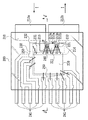
- FIG. 1 is a top view showing a configuration example of the current sensor 1 according to the first embodiment.
- the current sensor 1 includes, for example, a conductor 210 for passing a current to be measured I having two lead terminals 212a and 212b, a signal processing IC 220, and a metal for supporting the signal processing IC 220.
- a plate 230 and, for example, ten lead terminals 241 are provided.
- the number of lead terminals 212a, 212b, and 241 is not limited to the example shown in FIG. 1, and can be changed.
- the conductor 210 has a current path 211 through which the current I to be measured flows in the circumferential direction from the lead terminal 212a side to the lead terminal 212b side.
- a gap 210a is formed between the lead terminals 212a and 212b so as to follow the shape of the current path 211.
- the current path 211 has, for example, a U-shape, but if a current can be detected in a first magnetoelectric conversion element 213a and a second magnetoelectric conversion element 213b described later, the current path 211 is shown in FIG.
- a U-shape, a V-shape, a C-shape, or similar shapes can be applied.
- the first magnetoelectric conversion element 213a is disposed, and the second magnetoelectric conversion element 213b is disposed with the current path 211 interposed therebetween.
- the magnetoelectric conversion element 213 b is disposed in the gap 210 b between the conductor 210 and the metal plate 230.
- the metal plate 230 has a concave portion 231 in which a central portion of the metal plate 230 is recessed toward the conductor 210 in a plan view. Both ends have protrusions 232 that project toward the conductor 210 side.
- the concave portion 231 is formed to have a concave portion 231 that is recessed in one step, for example.
- the conductor 210 has a convex portion 215 formed along the concave portion 231 and the protruding portion 232 of the metal plate 230 in plan view. That is, the convex portion 215 is formed such that the conductor 210 protrudes toward the metal plate 230 in a plan view.
- the insulating member 214 is supported not by the conductor 210 side but by at least the protruding portion 232 on the back surface of the metal plate 230.
- the insulating member 214 may be supported by the back surface of the metal plate 230 other than the protruding portion 232 (for example, the side portions on both sides of the concave portion 231 or / and the bottom portion of the concave portion 231).
- the convex-shaped part 215 and the concave-shaped part 231 illustrated about the case where a shape changes in one step, you may comprise in steps, for example so that it may become two steps or more.
- the convex portion 215 may be gradually or continuously projected from the conductor 210 (peripheral portion of the gap 210a), and the concave portion 231 may be gradually along the protruding shape of the conductor 210. Or you may make it form a hollow continuously.
- the conductor 210 preferably satisfies a thickness of 0.15 mm or less and a resistance value of 2 m ⁇ or less from the viewpoint of preventing heat generation.
- Examples of the magnetoelectric conversion elements 213a and 213b include a Hall element, a magnetoresistive effect element, a Hall IC, and a magnetoresistive effect IC.
- the conductor 210, the lead terminal 241, the signal processing IC 220, and the magnetoelectric conversion elements 213a and 213b are sealed with a mold resin (mold member) 280 as shown in FIG. Formed as.
- the mold resin 280 is a mold resin such as an epoxy resin.
- the magnetoelectric conversion element 213a is disposed in the gap 210a adjacent to the U-shaped current path 211, detects the magnetic flux density generated by the current to be measured I flowing in the conductor 210, and responds to the magnetic flux density.
- the electrical signal is output to the signal processing IC 220.
- the magnetoelectric conversion element 213b also detects the magnetic flux density generated by the measured current I flowing through the conductor 210, and outputs an electrical signal corresponding to the magnetic flux density to the signal processing IC 220. In this way, the magnetoelectric conversion elements 213a and 213b perform current detection according to the measured current I flowing through the conductor 210.
- the magnetoelectric conversion elements 213a and 213b are spaced apart from the conductor 210 by gaps 210a and 210b, respectively, and are not in contact with the conductor 210 at all times. Thereby, the conductor 210 and the magnetoelectric conversion elements 213a and 213b are not electrically connected, and a gap (clearance) for maintaining insulation is secured.
- the distance between the conductor 210 and the magnetoelectric conversion element 213a and the distance w between the conductor 210 and the magnetoelectric conversion element 213b are, for example, 50 ⁇ m or more and 150 ⁇ m or less in plan view.
- the distance w between the conductor 210 and the magnetoelectric conversion elements 213a and 213b is less than 50 ⁇ m, there is a concern about a decrease in withstand voltage, and when the distance w is greater than 150 ⁇ m, the magnetoelectric conversion element 213a when current flows through the conductor 210. , 213b is likely to reduce the magnetic field detected and reduce the detection accuracy.
- the magnetoelectric conversion element 213a is supported by an insulating member 214 (shown by a broken line in FIG. 1).
- an insulating member 214 for example, an insulating tape made of a polyimide material having a high withstand voltage is used.
- the insulating member 214 is not limited to a polyimide tape, and for example, an insulating sheet in which an adhesive is applied to a polyimide material or a ceramic material can also be applied.
- the metal plate 230 is in contact with the insulating member 214, and a part of the lead terminal 241 is exposed from the mold resin 280.
- the magnetoelectric conversion elements 213a and 213b are electrically connected to the signal processing IC 220 via a wire (metal wire) 260, and the signal processing IC 220 is electrically connected to the lead terminal 241 via a wire (metal wire) 250.
- the signal processing IC 220 is configured by, for example, an LSI (Large Scale Integration), and in this embodiment, includes a memory, a processor, a bias circuit, a subtraction circuit, a correction circuit, an amplification circuit, and the like.
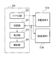
- the configuration of the signal processing IC 220 is shown in a detailed functional block diagram in FIG. 3 to be described later.
- FIG. 2 is a side view taken along the line J-J ′ of the current sensor 1 shown in FIG.
- the insulating member 214 is joined to a part of the back surface 230A of the metal plate 230 so as to support the magnetoelectric conversion element 213a.
- the magnetoelectric conversion element 213a is shown, but the magnetoelectric conversion element 213b is also arranged in the same manner as the magnetoelectric conversion element 213a.
- a step 201 is formed on a part of the back surface of the conductor 210 constituting the gap 210a, and the conductor 210 is always arranged so as not to contact the insulating member 214 by the step 201.
- the step 201 shown in FIG. 2 is for preventing the creeping surface formed when the insulator is in contact with the conductive material between the insulating member 214 and the conductor 210.
- a step may be provided in the conductor 210 facing the insulating member 214, and the insulating member 214 may be disposed in a space within the step.
- the conductor 210 and the insulating member 214 are not reliably in contact with each other, and as a result, the conductor 210 does not support the insulating member 214.
- the steps described above can be formed by coining, half-cutting, or downset, for example.
- the space between the back surface of the conductor 210 and the insulating member 214 is filled with a mold resin 280.
- the mold resin 280 has a water absorption rate of, for example, 0.5% or less. By doing so, since the expansion of the mold resin 280 can be suppressed, it is possible to prevent the stress applied to the magnetoelectric conversion elements 213a and 213b from being applied.
- the withstand voltage performance is reduced as compared with the case where the insulating member 214 and the conductor 210 are not configured to be in contact with each other. .
- the step 201 portion of the conductor 210 is more than the insulating member 214 so that the insulating member 214 and the conductor 210 are not in contact with each other by forming the step 201 on the conductor 210. It is located above.
- the insulating member 214 does not contact the conductor 210 and no creepage is formed between the primary side (conductor 210 side) and the secondary side of the current sensor 1. Therefore, no creepage is formed inside the current sensor, so that the withstand voltage performance of the current sensor 1 is maintained, and the occurrence of withstand voltage deterioration due to changes in the operating environment can be suppressed.
- the insulating member 214 is made of, for example, an insulating tape made of polyimide material having excellent pressure resistance, and is attached to the back surface 230A of the metal plate 230 in a state as shown in FIG. 2 to support the magnetoelectric conversion element 213a from the back surface.
- the conductor 210 and the magnetoelectric conversion element 213a are provided on the same surface of the insulating member 214.
- the height position of the magnetosensitive surface 216 of the magnetoelectric conversion element 213 is set between the height from the bottom surface to the top surface of the conductor 210 (for example, the center), so that the magnetosensitive surface 216 of the magnetoelectric conversion element 213a
- FIG. 3 is a functional block diagram of an example of the signal processing IC 220.
- the signal processing IC 220 includes a bias circuit 201, a subtraction circuit 202, a correction circuit 203, and an amplification circuit 204.
- the bias circuit 201 is connected to the magnetoelectric conversion elements 213a and 213b and supplies power to the magnetoelectric conversion elements 213a and 213b.
- the bias circuit 201 is a circuit for applying (inflowing) an excitation current to the magnetoelectric conversion elements 213a and 213b.
- the subtraction circuit 202 calculates the current value by canceling the influence of the magnetic field generated externally (cancelling in-phase noise) based on the difference between the outputs of the pair of magnetoelectric conversion elements 213a and 213b.
- V1 and V2 are expressed by the following equations.
- V1 S1 ⁇ (B1 + BE)
- V2 S2 ⁇ ( ⁇ B2 + BE) (4)
- the subtraction circuit 202 shown in FIG. 3 is configured to calculate the difference between the output signals from the magnetoelectric conversion elements 213a and 213b, for example.
- the correction circuit 203 is configured to correct the output value from the subtraction circuit 202. For example, based on the operating temperature, the output value of the magnetoelectric conversion elements 213a and 213b according to the temperature correction coefficient stored in the memory in advance. Is to be corrected. For this reason, current detection with low temperature dependence and high accuracy is possible.
- the amplification circuit 204 amplifies the output value from the correction circuit 203.
- the magnetoelectric conversion elements 213a and 213b are die-bonded on the insulating member 214 bonded to the lead frame, and the signal processing IC 220 is die-bonded on the metal plate 230. Then, the magnetoelectric conversion elements 213a and 213b and the signal processing IC 220 are wire-bonded with wires 250 and 260. Next, the conductor 210, the magnetoelectric conversion elements 213a and 213b, the signal processing IC 220, and the metal plate 230 are molded with a molding resin 280 to perform lead cutting. Next, the high-voltage side lead terminals 212a and 212b and the low-voltage side lead terminals 241 are formed by forming.
- the conductor 210 and the signal processing IC 220 have a gap for electrically insulating the electric sensor 1 in a plan view or a side view. So it has excellent insulation resistance.
- the magnetoelectric conversion element 213a and the magnetoelectric conversion element 213b are arranged at different locations, the magnetoelectric conversion element 213a and the magnetoelectric conversion element 213b are subjected to different stresses. Since the sensitivity of the magnetoelectric conversion element varies depending on the stress, if different stresses are applied to the magnetoelectric conversion element 213a and the magnetoelectric conversion element 213b, the magnetic field detection accuracy may be lowered.
- the metal plate 230 is in contact with the insulating member 214, and a part of the lead terminal 241 is exposed from the mold resin 280. For this reason, even if the current to be measured I flows through the conductor 210 and heat is generated, the heat is quickly released through the insulating member 214 and the lead terminal 241. Thereby, the fall of magnetic field detection accuracy can be suppressed.
- the metal plate 230 has a concave portion 231 formed to be recessed on the opposite side to the conductor 210 side in a plan view, and a protruding portion 232 projecting toward the conductor 210 side.
- the conductor 210 includes a concave portion 231 of the metal plate 230 and a convex portion 215 formed along the protruding portion 232 as viewed from above. That is, the formation pattern of the convex portion 215 of the conductor 210 and the concave portion 231 and the protruding portion 232 of the metal plate 230 makes it easier to release heat when the current I to be measured flows through the conductor 210 to the lead terminal 241 side. . Thereby, the fall of magnetic field detection precision and the fall of disturbance magnetic field cancellation precision can be suppressed.
- the conductor 210 is formed so as to surround the periphery of the magnetoelectric conversion element 213a. Thereby, a magnetic field comes to act with respect to the magnetoelectric conversion element 213a, and as a result, the output signal of the magnetoelectric conversion element 213a becomes large. As a result, the detection accuracy of the current sensor 1 is further improved.
- the insulating member 214 is not in contact with the conductor 210 and is supported only by the metal plate 230, no creepage is formed between the conductor 210 and the insulating member 214, and the withstand voltage of the current sensor 1 is unlikely to decrease. Become.
- the die attach film 270 shown in FIG. 2 is attached to the back surface of the wafer before dicing the wafer, and therefore, unlike the case where the magnetoelectric conversion elements 213a and 213b are fixed using an insulating paste or conductive paste described later, Since the creeping surface does not extend so that the skirt portion is formed toward the conductor 210 around the magnetoelectric conversion elements 213a and 213b, the withstand voltage of the current sensor is further improved.
- the magnetoelectric conversion elements 213a and 213b are fixed on the insulating member 214 using a die bonding material.
- a conductive paste is used as the die bonding material, the magnetoelectric conversion elements are formed depending on the base portion of the paste. The insulation distance between 213a and 213b and the conductor 210 is reduced. Further, even when an insulating paste is used as the die bond material, the creeping surface can be formed by the skirt portion of the paste.
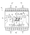
- FIG. 5 is a top view showing a configuration example of the current sensor 1A according to the second embodiment
- FIG. 6 is a side view taken along the line K-K ′ in FIG.
- the convex portions 15 (15a, 15b) of the conductor 10 also have a multi-stage shape (two-stage shape) in accordance with the shape of the concave portions 31 (31a, 31b) of the metal plate 30. It is characterized in that the resistance value of the entire conductor is reduced.
- Other configurations are the same as those in the first embodiment.
Landscapes
- Physics & Mathematics (AREA)
- General Physics & Mathematics (AREA)
- Measuring Instrument Details And Bridges, And Automatic Balancing Devices (AREA)
Abstract
Priority Applications (5)
| Application Number | Priority Date | Filing Date | Title |
|---|---|---|---|
| EP15811265.6A EP3163312B1 (fr) | 2014-06-27 | 2015-06-26 | Capteur de courant |
| CN201580025877.9A CN106461705B (zh) | 2014-06-27 | 2015-06-26 | 电流传感器 |
| KR1020167036165A KR101882126B1 (ko) | 2014-06-27 | 2015-06-26 | 전류 센서 |
| JP2016529088A JP6321800B2 (ja) | 2014-06-27 | 2015-06-26 | 電流センサ |
| US15/321,327 US10101368B2 (en) | 2014-06-27 | 2015-06-26 | Current sensor |
Applications Claiming Priority (2)
| Application Number | Priority Date | Filing Date | Title |
|---|---|---|---|
| JP2014-132862 | 2014-06-27 | ||
| JP2014132862 | 2014-06-27 |
Publications (1)
| Publication Number | Publication Date |
|---|---|
| WO2015198609A1 true WO2015198609A1 (fr) | 2015-12-30 |
Family
ID=54937714
Family Applications (1)
| Application Number | Title | Priority Date | Filing Date |
|---|---|---|---|
| PCT/JP2015/003230 Ceased WO2015198609A1 (fr) | 2014-06-27 | 2015-06-26 | Capteur de courant |
Country Status (6)
| Country | Link |
|---|---|
| US (1) | US10101368B2 (fr) |
| EP (1) | EP3163312B1 (fr) |
| JP (1) | JP6321800B2 (fr) |
| KR (1) | KR101882126B1 (fr) |
| CN (1) | CN106461705B (fr) |
| WO (1) | WO2015198609A1 (fr) |
Cited By (5)
| Publication number | Priority date | Publication date | Assignee | Title |
|---|---|---|---|---|
| JP2017134022A (ja) * | 2016-01-29 | 2017-08-03 | 旭化成エレクトロニクス株式会社 | 電流センサ及び製造方法 |
| WO2018051575A1 (fr) * | 2016-09-14 | 2018-03-22 | 旭化成エレクトロニクス株式会社 | Capteur de courant électrique |
| JP2021015116A (ja) * | 2019-07-10 | 2021-02-12 | 旭化成エレクトロニクス株式会社 | 電流センサおよび電流センサの製造方法 |
| JPWO2024177013A1 (fr) * | 2023-02-20 | 2024-08-29 | ||
| JP2024546171A (ja) * | 2021-12-21 | 2024-12-17 | 江▲蘇▼多▲維▼科技有限公司 | 電流センサ |
Families Citing this family (14)
| Publication number | Priority date | Publication date | Assignee | Title |
|---|---|---|---|---|
| US10698005B2 (en) | 2017-04-20 | 2020-06-30 | Asahi Kasei Microdevices Corporation | Magnetic detection device, current detection device, method for manufacturing magnetic detection device, and method for manufacturing current detection device |
| DE102018201425A1 (de) * | 2018-01-30 | 2019-08-01 | Osram Gmbh | Konversionsbaugruppe mit anschlussrahmen |
| US10755994B2 (en) * | 2018-10-29 | 2020-08-25 | Advanced Semiconductor Engineering, Inc. | Semiconductor package structure and semiconductor substrate |
| EP3671228B1 (fr) * | 2018-12-12 | 2023-03-29 | Melexis Technologies SA | Capteur de courant avec conducteur de courant intégré |
| JP2020095029A (ja) * | 2018-12-12 | 2020-06-18 | メレキシス テクノロジーズ エス エーMelexis Technologies SA | 電流センサ |
| CN112114180B (zh) * | 2019-06-20 | 2024-04-26 | 株式会社电装 | 电力转换装置 |
| CN114008464A (zh) * | 2019-08-26 | 2022-02-01 | 株式会社村田制作所 | 电流传感器 |
| US12345782B2 (en) * | 2021-09-29 | 2025-07-01 | Asahi Kasei Microdevices Corporation | Magnetic sensor |
| CN113866475B (zh) * | 2021-09-30 | 2025-02-18 | 意瑞半导体(上海)有限公司 | 电流传感器的引线框架及电流传感器 |
| WO2023167096A1 (fr) * | 2022-03-03 | 2023-09-07 | 旭化成エレクトロニクス株式会社 | Capteur de courant et procédé de détection de courant |
| JP7328430B1 (ja) * | 2022-10-04 | 2023-08-16 | 旭化成エレクトロニクス株式会社 | 電流センサ |
| JP7329115B1 (ja) * | 2022-10-04 | 2023-08-17 | 旭化成エレクトロニクス株式会社 | 電流センサ |
| JP7328429B1 (ja) * | 2022-10-04 | 2023-08-16 | 旭化成エレクトロニクス株式会社 | 電流センサ |
| JP7329118B1 (ja) * | 2022-10-24 | 2023-08-17 | 旭化成エレクトロニクス株式会社 | 電流センサ |
Citations (3)
| Publication number | Priority date | Publication date | Assignee | Title |
|---|---|---|---|---|
| JP2007073803A (ja) * | 2005-09-08 | 2007-03-22 | Toshiba Corp | 半導体装置及びその製造方法 |
| WO2013008462A1 (fr) * | 2011-07-13 | 2013-01-17 | 旭化成エレクトロニクス株式会社 | Substrat de capteur de courant et capteur de courant |
| JP2013245942A (ja) * | 2012-05-23 | 2013-12-09 | Asahi Kasei Electronics Co Ltd | 電流センサ |
Family Cites Families (13)
| Publication number | Priority date | Publication date | Assignee | Title |
|---|---|---|---|---|
| CH670004A5 (fr) * | 1986-02-10 | 1989-04-28 | Landis & Gyr Ag | |
| JP2001165963A (ja) * | 1999-12-09 | 2001-06-22 | Sanken Electric Co Ltd | ホール素子を備えた電流検出装置 |
| JP4164615B2 (ja) * | 1999-12-20 | 2008-10-15 | サンケン電気株式会社 | ホ−ル素子を備えた電流検出装置 |
| EP1267173A3 (fr) * | 2001-06-15 | 2005-03-23 | Sanken Electric Co., Ltd. | Détecteur de courant à effet Hall |
| JP2003172750A (ja) * | 2001-09-26 | 2003-06-20 | Sanken Electric Co Ltd | 電流検出装置 |
| US7709754B2 (en) * | 2003-08-26 | 2010-05-04 | Allegro Microsystems, Inc. | Current sensor |
| US20060219436A1 (en) * | 2003-08-26 | 2006-10-05 | Taylor William P | Current sensor |
| JP4833111B2 (ja) * | 2006-09-20 | 2011-12-07 | 株式会社東海理化電機製作所 | 電流検出器 |
| US9222992B2 (en) * | 2008-12-18 | 2015-12-29 | Infineon Technologies Ag | Magnetic field current sensors |
| US8400139B2 (en) * | 2010-03-26 | 2013-03-19 | Infineon Technologies Ag | Sensor package having a sensor chip |
| JP2012229950A (ja) * | 2011-04-25 | 2012-11-22 | Asahi Kasei Electronics Co Ltd | 電流センサおよび電流センサの製造方法 |
| WO2013008466A1 (fr) | 2011-07-13 | 2013-01-17 | 旭化成エレクトロニクス株式会社 | Substrat de capteur de courant et capteur de courant |
| US8907437B2 (en) * | 2011-07-22 | 2014-12-09 | Allegro Microsystems, Llc | Reinforced isolation for current sensor with magnetic field transducer |
-
2015
- 2015-06-26 CN CN201580025877.9A patent/CN106461705B/zh active Active
- 2015-06-26 KR KR1020167036165A patent/KR101882126B1/ko active Active
- 2015-06-26 US US15/321,327 patent/US10101368B2/en active Active
- 2015-06-26 EP EP15811265.6A patent/EP3163312B1/fr active Active
- 2015-06-26 WO PCT/JP2015/003230 patent/WO2015198609A1/fr not_active Ceased
- 2015-06-26 JP JP2016529088A patent/JP6321800B2/ja active Active
Patent Citations (3)
| Publication number | Priority date | Publication date | Assignee | Title |
|---|---|---|---|---|
| JP2007073803A (ja) * | 2005-09-08 | 2007-03-22 | Toshiba Corp | 半導体装置及びその製造方法 |
| WO2013008462A1 (fr) * | 2011-07-13 | 2013-01-17 | 旭化成エレクトロニクス株式会社 | Substrat de capteur de courant et capteur de courant |
| JP2013245942A (ja) * | 2012-05-23 | 2013-12-09 | Asahi Kasei Electronics Co Ltd | 電流センサ |
Non-Patent Citations (1)
| Title |
|---|
| See also references of EP3163312A4 * |
Cited By (9)
| Publication number | Priority date | Publication date | Assignee | Title |
|---|---|---|---|---|
| JP2017134022A (ja) * | 2016-01-29 | 2017-08-03 | 旭化成エレクトロニクス株式会社 | 電流センサ及び製造方法 |
| WO2018051575A1 (fr) * | 2016-09-14 | 2018-03-22 | 旭化成エレクトロニクス株式会社 | Capteur de courant électrique |
| JPWO2018051575A1 (ja) * | 2016-09-14 | 2019-08-08 | 旭化成エレクトロニクス株式会社 | 電流センサ |
| JP2021015116A (ja) * | 2019-07-10 | 2021-02-12 | 旭化成エレクトロニクス株式会社 | 電流センサおよび電流センサの製造方法 |
| JP7420640B2 (ja) | 2019-07-10 | 2024-01-23 | 旭化成エレクトロニクス株式会社 | 電流センサおよび電流センサの製造方法 |
| JP2024546171A (ja) * | 2021-12-21 | 2024-12-17 | 江▲蘇▼多▲維▼科技有限公司 | 電流センサ |
| JP7812449B2 (ja) | 2021-12-21 | 2026-02-09 | 江▲蘇▼多▲維▼科技有限公司 | 電流センサ |
| JP7812449B6 (ja) | 2021-12-21 | 2026-03-02 | 江▲蘇▼多▲維▼科技有限公司 | 電流センサ |
| JPWO2024177013A1 (fr) * | 2023-02-20 | 2024-08-29 |
Also Published As
| Publication number | Publication date |
|---|---|
| CN106461705B (zh) | 2019-04-30 |
| US10101368B2 (en) | 2018-10-16 |
| EP3163312A4 (fr) | 2017-07-26 |
| JP6321800B2 (ja) | 2018-05-09 |
| EP3163312B1 (fr) | 2019-05-22 |
| EP3163312A1 (fr) | 2017-05-03 |
| US20170160313A1 (en) | 2017-06-08 |
| CN106461705A (zh) | 2017-02-22 |
| KR101882126B1 (ko) | 2018-07-25 |
| JPWO2015198609A1 (ja) | 2017-04-20 |
| KR20170008864A (ko) | 2017-01-24 |
Similar Documents
| Publication | Publication Date | Title |
|---|---|---|
| JP6321800B2 (ja) | 電流センサ | |
| JP6415148B2 (ja) | 電流センサ | |
| US8760149B2 (en) | Magnetic field current sensors | |
| JP6017182B2 (ja) | 電流センサ | |
| JP6234263B2 (ja) | 電流センサ | |
| TW201314216A (zh) | 電流感測器用基板及電流感測器 | |
| JP6505505B2 (ja) | 電流センサ | |
| JP2018179994A (ja) | 磁気検出装置、電流検出装置、磁気検出装置の製造方法、及び電流検出装置の製造方法 | |
| US11360122B2 (en) | Current sensor and method for manufacturing current sensor | |
| JP6346738B2 (ja) | 電流センサ | |
| TWI485411B (zh) | Current sensor substrate and current sensor | |
| JP2017134022A (ja) | 電流センサ及び製造方法 | |
| JP2021025785A (ja) | 電流センサおよび電流センサの製造方法 | |
| RU2465609C1 (ru) | Бесконтактный измеритель тока | |
| JP7420640B2 (ja) | 電流センサおよび電流センサの製造方法 | |
| JP2024053775A (ja) | 電流センサ | |
| JP2024125164A (ja) | 電流センサ | |
| US12571819B2 (en) | Current sensor | |
| CN118584173A (zh) | 电流传感器 | |
| JP2025013224A (ja) | 電流センサ |
Legal Events
| Date | Code | Title | Description |
|---|---|---|---|
| 121 | Ep: the epo has been informed by wipo that ep was designated in this application |
Ref document number: 15811265 Country of ref document: EP Kind code of ref document: A1 |
|
| ENP | Entry into the national phase |
Ref document number: 2016529088 Country of ref document: JP Kind code of ref document: A |
|
| WWE | Wipo information: entry into national phase |
Ref document number: 15321327 Country of ref document: US |
|
| ENP | Entry into the national phase |
Ref document number: 20167036165 Country of ref document: KR Kind code of ref document: A |
|
| REEP | Request for entry into the european phase |
Ref document number: 2015811265 Country of ref document: EP |
|
| WWE | Wipo information: entry into national phase |
Ref document number: 2015811265 Country of ref document: EP |
|
| NENP | Non-entry into the national phase |
Ref country code: DE |