WO2015199228A1 - Détecteur de force - Google Patents
Détecteur de force Download PDFInfo
- Publication number
- WO2015199228A1 WO2015199228A1 PCT/JP2015/068544 JP2015068544W WO2015199228A1 WO 2015199228 A1 WO2015199228 A1 WO 2015199228A1 JP 2015068544 W JP2015068544 W JP 2015068544W WO 2015199228 A1 WO2015199228 A1 WO 2015199228A1
- Authority
- WO
- WIPO (PCT)
- Prior art keywords
- force
- sensor element
- base substrate
- force sensor
- soldering
- Prior art date
- Legal status (The legal status is an assumption and is not a legal conclusion. Google has not performed a legal analysis and makes no representation as to the accuracy of the status listed.)
- Ceased
Links
Images



Classifications
-
- G—PHYSICS
- G01—MEASURING; TESTING
- G01L—MEASURING FORCE, STRESS, TORQUE, WORK, MECHANICAL POWER, MECHANICAL EFFICIENCY, OR FLUID PRESSURE
- G01L1/00—Measuring force or stress, in general
- G01L1/26—Auxiliary measures taken, or devices used, in connection with the measurement of force, e.g. for preventing influence of transverse components of force, for preventing overload
-
- G—PHYSICS
- G01—MEASURING; TESTING
- G01L—MEASURING FORCE, STRESS, TORQUE, WORK, MECHANICAL POWER, MECHANICAL EFFICIENCY, OR FLUID PRESSURE
- G01L1/00—Measuring force or stress, in general
- G01L1/18—Measuring force or stress, in general using properties of piezo-resistive materials, i.e. materials of which the ohmic resistance varies according to changes in magnitude or direction of force applied to the material
-
- G—PHYSICS
- G01—MEASURING; TESTING
- G01L—MEASURING FORCE, STRESS, TORQUE, WORK, MECHANICAL POWER, MECHANICAL EFFICIENCY, OR FLUID PRESSURE
- G01L5/00—Apparatus for, or methods of, measuring force, work, mechanical power, or torque, specially adapted for specific purposes
-
- G—PHYSICS
- G01—MEASURING; TESTING
- G01L—MEASURING FORCE, STRESS, TORQUE, WORK, MECHANICAL POWER, MECHANICAL EFFICIENCY, OR FLUID PRESSURE
- G01L19/00—Details of, or accessories for, apparatus for measuring steady or quasi-steady pressure of a fluent medium insofar as such details or accessories are not special to particular types of pressure gauges
- G01L19/0061—Electrical connection means
-
- G—PHYSICS
- G01—MEASURING; TESTING
- G01L—MEASURING FORCE, STRESS, TORQUE, WORK, MECHANICAL POWER, MECHANICAL EFFICIENCY, OR FLUID PRESSURE
- G01L19/00—Details of, or accessories for, apparatus for measuring steady or quasi-steady pressure of a fluent medium insofar as such details or accessories are not special to particular types of pressure gauges
- G01L19/0061—Electrical connection means
- G01L19/0069—Electrical connection means from the sensor to its support
-
- G—PHYSICS
- G01—MEASURING; TESTING
- G01L—MEASURING FORCE, STRESS, TORQUE, WORK, MECHANICAL POWER, MECHANICAL EFFICIENCY, OR FLUID PRESSURE
- G01L19/00—Details of, or accessories for, apparatus for measuring steady or quasi-steady pressure of a fluent medium insofar as such details or accessories are not special to particular types of pressure gauges
- G01L19/0061—Electrical connection means
- G01L19/0084—Electrical connection means to the outside of the housing
-
- G—PHYSICS
- G01—MEASURING; TESTING
- G01L—MEASURING FORCE, STRESS, TORQUE, WORK, MECHANICAL POWER, MECHANICAL EFFICIENCY, OR FLUID PRESSURE
- G01L19/00—Details of, or accessories for, apparatus for measuring steady or quasi-steady pressure of a fluent medium insofar as such details or accessories are not special to particular types of pressure gauges
- G01L19/14—Housings
- G01L19/142—Multiple part housings
-
- G—PHYSICS
- G01—MEASURING; TESTING
- G01L—MEASURING FORCE, STRESS, TORQUE, WORK, MECHANICAL POWER, MECHANICAL EFFICIENCY, OR FLUID PRESSURE
- G01L19/00—Details of, or accessories for, apparatus for measuring steady or quasi-steady pressure of a fluent medium insofar as such details or accessories are not special to particular types of pressure gauges
- G01L19/14—Housings
- G01L19/147—Details about the mounting of the sensor to support or covering means
-
- G—PHYSICS
- G01—MEASURING; TESTING
- G01L—MEASURING FORCE, STRESS, TORQUE, WORK, MECHANICAL POWER, MECHANICAL EFFICIENCY, OR FLUID PRESSURE
- G01L19/00—Details of, or accessories for, apparatus for measuring steady or quasi-steady pressure of a fluent medium insofar as such details or accessories are not special to particular types of pressure gauges
- G01L19/14—Housings
- G01L19/148—Details about the circuit board integration, e.g. integrated with the diaphragm surface or encapsulation
-
- G—PHYSICS
- G01—MEASURING; TESTING
- G01L—MEASURING FORCE, STRESS, TORQUE, WORK, MECHANICAL POWER, MECHANICAL EFFICIENCY, OR FLUID PRESSURE
- G01L9/00—Measuring steady of quasi-steady pressure of fluid or fluent solid material by electric or magnetic pressure-sensitive elements; Transmitting or indicating the displacement of mechanical pressure-sensitive elements, used to measure the steady or quasi-steady pressure of a fluid or fluent solid material, by electric or magnetic means
- G01L9/0041—Transmitting or indicating the displacement of flexible diaphragms
- G01L9/0051—Transmitting or indicating the displacement of flexible diaphragms using variations in ohmic resistance
- G01L9/0052—Transmitting or indicating the displacement of flexible diaphragms using variations in ohmic resistance of piezoresistive elements
-
- G—PHYSICS
- G01—MEASURING; TESTING
- G01L—MEASURING FORCE, STRESS, TORQUE, WORK, MECHANICAL POWER, MECHANICAL EFFICIENCY, OR FLUID PRESSURE
- G01L9/00—Measuring steady of quasi-steady pressure of fluid or fluent solid material by electric or magnetic pressure-sensitive elements; Transmitting or indicating the displacement of mechanical pressure-sensitive elements, used to measure the steady or quasi-steady pressure of a fluid or fluent solid material, by electric or magnetic means
- G01L9/0041—Transmitting or indicating the displacement of flexible diaphragms
- G01L9/0051—Transmitting or indicating the displacement of flexible diaphragms using variations in ohmic resistance
- G01L9/0052—Transmitting or indicating the displacement of flexible diaphragms using variations in ohmic resistance of piezoresistive elements
- G01L9/0054—Transmitting or indicating the displacement of flexible diaphragms using variations in ohmic resistance of piezoresistive elements integral with a semiconducting diaphragm
Definitions
- the present invention relates to a force detector that outputs a signal corresponding to the magnitude of an applied force, and more particularly to a force detector that can be miniaturized by preventing a short circuit between electrodes.
- a force detector that outputs a signal corresponding to the magnitude of the transmitted force has been put into practical use.
- the force applied to the force transmission ball is transmitted to the force sensor element.
- the force transmission ball and the force sensor element are housed in a storage case.
- the uppermost portion of the force transmission ball protrudes from a through hole formed in the upper wall portion of the storage case, and the force sensor element is in the bottom wall portion of the storage case. It arrange
- An input / output terminal connected to the force sensor element is exposed to the outside on the bottom wall portion (or the side wall portion near the bottom wall portion) of the storage case, and the substrate is disposed on the outer wall surface side of the bottom wall portion.
- the force detector is mounted on the substrate by being connected to the substrate by soldering.
- soldering portions Patent Document 1, JP 2011-169717 A.
- a gap generated between the bottom wall portion and the substrate when the input / output terminals of the force detector are soldered to the electrodes on the substrate Therefore, even when a force is applied to the force sensor element from above through the force transmission ball, the bottom wall portion of the storage case located below the force sensor element bends to absorb a part of the force. Disappear. As a result, variations in detection accuracy can be suppressed.
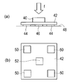
- FIG. 3 shows the principle of the configuration for preventing the variation in detection accuracy as described above.
- the storage case shows only the bottom wall portion 42.
- the force sensor element 40 is placed on the central portion of the inner wall surface of the bottom wall portion 42 of the storage case.
- a soldering land pattern is formed on the outer wall surface of the bottom wall portion 42 as shown in FIG.
- the force sensor element is connected to a soldering electrode (not shown) on the substrate 48 via solder portions 44 and 46 via a soldering land pattern.
- FIG. 3B shows a land pattern on the outer wall surface of the bottom wall portion 42.
- the four land patterns 50 arranged near the four corners of the outer wall surface of the square bottom wall portion 42 function as input / output terminals of the force sensor element 40, and are connected to the electrodes on the substrate 48 by the solder portions 44, respectively.
- the land pattern 52 is not electrically connected to the force sensor element 40, and fills a part of the gap between the outer wall surface of the bottom wall portion 42 and the substrate 48 with the solder portion 46. . That is, if a downward force f as seen in FIG. 3A is applied to the force sensor element 40, the bottom wall portion 42 has four corners relative to the substrate 48 if the solder 46 does not exist at the position of the land pattern 52.
- the vicinity of the center of the bottom wall portion 42 bends in a direction approaching the substrate 48 and absorbs at least a part of the force f, resulting in variations in detection accuracy. If there is the solder part 46, the bottom wall part 42 will not bend, so that the force sensor element 40 can output a signal accurately corresponding to the magnitude of the force f.
- Patent Document 2 discloses a structure in which a fixing terminal is provided on the back surface of a package substrate of a force sensor package so as to overlap with the adhesive fixing position of the sensor structure in a plane. Yes.
- the dual-purpose terminal 33 in which the SMD terminal 31 and the fixing terminal 32 are integrally provided is provided.
- the force detector may need to be removed from the soldered board depending on the need for replacement or repair.
- the force detector shown in FIG. 4 is removed from the substrate, the solder is heated and melted.
- the solder 44 at the four corners of the bottom wall portion 42 is located in the vicinity of the outer peripheral portion of the bottom wall portion 42, for example, by directly applying a soldering iron to the electrode on the substrate 48 or the solder portion 44 attached to the electrode. Can be heated.
- a soldering iron cannot be applied to the solder 46 located near the center of the bottom wall portion 42.
- An object of the present invention is to provide a force detector that can prevent a short circuit between electrodes and can be miniaturized.
- the force detector of the present invention includes a force sensor element mounted on the surface of the base substrate, a force transmission member that transmits force to the force sensor element, and a solder that is provided on the back surface of the base substrate and exposed to the outside. A plurality of terminals. A soldering portion formed of a solderable material is provided in a predetermined region centered on a position where a virtual extension line of a force applied from the force transmission member to the force sensor element passes through the base substrate.
- the projection area obtained by projecting the deformation area of the force sensor element that is deformed when the force transmission member transmits force to the force sensor element on the base substrate is included in the predetermined area.
- the terminal is composed of four solder land electrodes respectively formed at the four corners of the base substrate. The shapes of the four solder land electrodes are determined so that a part of the terminal electrode exists in the above-described projection area to constitute a solder portion. In the present invention, all of the four soldering land electrodes existing in the projection region constitute a soldering portion.
- the force detector can be made smaller than before.
- a virtual extension line of a force applied from the force transmission member to the force sensor element is formed in a predetermined region centered on a position passing through the substrate.
- the solder is applied by applying heat from the outside to the terminal part of which constitutes the soldering part.
- the force detector can be removed from the substrate by melting the solder attached to the attachment portion.
- the position and size of a part of the four solder receiving land electrodes constituting the soldering portion vary depending on the configuration of the force detector. That is, the size, shape, and material of each force detector and each member, particularly the shape of the bottom surface of the force sensor element, the thickness and material of the bottom wall of the storage case, and the force sensor element occupy the inner wall surface of the bottom wall. In consideration of the area and position, the magnitude of the force applied from the force transmission member to the force sensor element, and the like, the positions and sizes of some of the four solder receiving land electrodes are determined.
- the four solder land electrodes are preferably formed so that the distance between two adjacent terminal electrodes is 0.1 mm or more in order to prevent a short circuit. This distance can be further reduced by improving the soldering technique.
- the outline shape of the four solder land electrodes can be, for example, a quadrangular shape.
- the shape dimensions of the soldering land electrodes are determined so that one corner of each of the four soldering land electrodes is located within the above-described projection region.
- the force sensor element can be made of a semiconductor force sensor element in which a plurality of diffusion resistors are formed in the deformation region, and the force transmission member can be made of a sphere.
- the method of applying heat to the terminals is not limited to the method of applying heat directly to the terminals on the force detector side, but may be applied indirectly to the soldered part by applying heat to the electrodes on the board. Good.
- FIG. 1 shows one embodiment of the force detector of the present invention
- FIG. 1 (a) is a plan view showing a state in which the force detector is mounted on a substrate
- FIG. 1 (b) is FIG.
- FIG. 1B is a cross-sectional view taken along the line bb of FIG. 1A
- FIG. (A) And (b) is a figure similar to FIG.1 (b) which shows other embodiment and further embodiment of the force detector of this invention, respectively.
- (A) And (b) is a figure used in order to demonstrate the principle of variation in the detection accuracy in the conventional force detector.
- FIGS. 4A to 4D are a plan view, a right side view, a bottom view, and a sectional view taken along the line dd in FIG. 4A of another embodiment of the force detector of the present invention.
- the force detector of the present invention includes a storage case 10, a force sensor element 12 stored in the storage case 10, and a force transmission that transmits a force to the force sensor element 12. It has a force transmission ball 14 as a member, and four land electrodes 16 [see FIG. 1C] which are a plurality of solderable terminals fixed to the storage case 10 and exposed to the outside.
- the storage case 10 includes a bottom wall portion made of a base substrate 22, a peripheral wall portion 24, and an upper wall portion 28.
- the force sensor element 12 is placed on the inner wall surface or front surface of the base substrate 22 of the storage case 10, and four soldering land electrodes 16 having a rectangular outline are fixed to the outer wall surface or back surface of the base substrate 22.
- the peripheral wall portion 24 extends upward in FIG. 1B from the outer peripheral edge portion of the base substrate 22, and the contour shape viewed from above has a quadrangular shape.
- the upper wall portion 28 extends in the horizontal direction so as to cover the opening of the peripheral wall portion 24, and a through hole 26 is provided at the center.
- the force transmission ball 14 has an upper portion protruding upward from the through hole 26 of the upper wall portion 28 and a lower portion in contact with the force sensor element 12, and transmits the force applied from above to the force sensor 12.
- the force sensor element 12 is a semiconductor force sensor element.
- the semiconductor force sensor four diffusion resistors constituting a bridge circuit are formed in a diaphragm region (deformation region) by diffusing boron or the like in a silicon substrate, and the force transmitted by the force transmission sphere 14 is converted into a piezoresistor. The effect is converted into an electrical signal and output.
- the force detector has four landed soldering land electrodes 16 as shown in FIG. 1C as four input / output terminals (Vcc, + OUTPUT, GND, ⁇ OUTPUT) for the bridge circuit. It is provided on the outer wall surface of the bottom wall portion 22. As shown in FIG. 1C, the four solder land electrodes 16 formed at the four corners of the base substrate 22 of the storage case 10 are sized to cover most of the back surface of the base substrate 22 with four squares. Have. These soldering land electrodes 16 are formed so that an electrode pattern made of a metal with good solder wettability is exposed on the back surface of the base substrate 22. In the present embodiment, among the four corners of the four land electrodes 16, the four corners 16A located at the center of the base substrate 22 constitute the soldering part 30a as a whole.
- the four corners 16 ⁇ / b> A of the four soldered land electrodes 16 have a virtual extension line L of the force applied from the force transmission sphere 14 to the force sensor element 12 passing through the base substrate 22. It is included in a predetermined region R1 centered on the position. As shown in FIGS. 1B and 1C, the predetermined region R1 in the present embodiment has a dimension of one side d2 projected from the outer contour of the bottom surface of the force sensor element 12 to the back surface of the base substrate 22. It has a quadrilateral outline.
- soldering part 30a comprised by the four corner
- the projected area R2 is included in the projected area R2 having a quadrangular outline whose dimension is d1. That is, one corner 16A closest to the center point of the square outer wall surface of the base substrate 22 of each of the four land electrodes 16 is located in the projection region R2.
- the force detector is mounted on the mounting substrate 20 by bonding the soldering land electrode 16 to the soldering electrode 19 provided on the surface of the mounting substrate 20 via the solder portion 18. Is done.
- the gap between the soldering electrodes 19 on the mounting substrate 20 and the gap between the four soldering land electrodes 16 are determined by soldering between the soldering electrodes 19 adjacent to each other by the solder portion 18 or between the soldering land electrodes 16 adjacent to each other. It is determined not to be short-circuited.
- the four land electrodes 16 and the soldering electrodes 19 are formed such that the distance between two adjacent electrodes is 0.1 mm or more.
- the force applied to the force sensor element 12 mounted on the mounting substrate 20 is applied to the mounting substrate 20 via the soldering portion 30a. It is transmitted. As a result, bending of the base substrate 22 can be suppressed or prevented.
- each soldering land electrode 16 is arranged closer to the center than the edge of the back surface of the base substrate 22, so that each soldering land electrode 16 cannot be directly heated. It is heated indirectly by placing a soldering electrode on the soldering electrode.
- the land electrode pattern including the soldering portion has symmetry so that the bending of the bottom wall portion can be suppressed without causing as much deviation as possible.
- the land electrode pattern on the outer wall surface of the base substrate 22 shown in FIG. 1C is symmetrical with respect to two center lines that connect the centers of two opposing sides of two squares and two diagonal lines. And is point-symmetric about the center point of the square.
- the predetermined area where the soldering part is formed and the range of the projection area differ depending on the type of each force detector.
- 2A and 2B show a force detector on which force sensor elements each having a structure different from that of the force sensor element 12 shown in FIG. 1 are mounted.
- the force sensor element 36 in the force detector of FIG. 2A has a slightly wider deformation area than the force sensor element 12 of FIG. 1, and therefore the projection area R2 is also more than the projection area R2 of FIG. Slightly wider.
- the force sensor element 38 in FIG. 2B has a structure in which a peripheral pedestal supports a diaphragm forming a deformation region, and the projection region R2 is also slightly wider than the projection region R2 in FIG.
- FIG. 4 (a) to 4 (d) show a plan view, a right side view, a bottom view, and a cross-section taken along the line dd of FIG. 4 (a) of another embodiment of the force detector of the present invention.
- the same parts as those of the force detector of the embodiment shown in FIG. 1 are denoted by the reference numerals in which the number of reference numerals in FIG. Comparing the embodiment of FIG. 1 with the embodiment of FIG. 4, the configuration of the force sensor element 112, the structure of the storage case 110, and the shape and position of the soldering land electrode 116 are different.
- the force sensor element 112 has a structure in which a semiconductor force sensor element 112B is mounted on a glass base 112A.
- a gel-like protective layer 113 is formed on the semiconductor force sensor element 112B.
- the storage case 110 is composed of a metal cap and a circuit board.
- the circuit board constitutes the base board 122.
- the semiconductor sensor element 112 ⁇ / b> B and the electrode on the circuit board constituting the base substrate 122 are connected by wire bonding 106.
- the soldering land electrodes 116 formed on the back surface of the rectangular circuit board constituting the base substrate 122 of the storage case 110 have a rectangular shape and are formed at the corners of the bottom surface of the rectangular shape. It is formed in a completely matched state. As a result, according to the present embodiment, when removing the force detector, heat from the outside can be directly transmitted to the soldering land electrode 116.
- the relationship between the position and size of the land electrode 116 and the position and size of the force sensor element 112 and the method for determining the distance between adjacent soldering land electrodes 116 are the same as in the above embodiment. Therefore, also in this embodiment, of the four corner portions of the four solder land electrodes 116, the four corner portions 116A located at the center portion of the base substrate 122 constitute the solder portions 130a. In order to prevent a short circuit, the four land electrodes 116 are formed such that the distance between two adjacent electrodes is 0.1 mm or more.
- soldering portion is configured, there is no dedicated soldering portion as in the prior art. Therefore, it is not necessary to provide a space for providing a dedicated soldering portion on the back surface of the base substrate, and the force detector can be made smaller than before.
- the force detector of the present invention by providing a soldering portion in a predetermined area, it is possible to suppress the bending of the bottom wall portion of the storage case and prevent the detection accuracy from being varied, and the terminal to be heated. The solder attached to the soldering portion can be melted by adding, so that the force detector can be removed from the substrate.
- R2 Projection area R1 Predetermined area 10,110 Storage case 12,112 Force sensor element 14,114 Force transmission ball 16,116 Soldering land electrode 18 Solder 20 Substrate 22, 122 Base substrate (bottom wall) 24 peripheral wall portion 26 through hole 28 upper wall portion 30a, 30b, 130a soldering portion 36, 38 force sensor element
Landscapes
- Physics & Mathematics (AREA)
- General Physics & Mathematics (AREA)
- Force Measurement Appropriate To Specific Purposes (AREA)
- Electric Connection Of Electric Components To Printed Circuits (AREA)
Abstract
Priority Applications (3)
| Application Number | Priority Date | Filing Date | Title |
|---|---|---|---|
| JP2016529681A JP6346279B2 (ja) | 2014-06-27 | 2015-06-26 | 力検出器 |
| US15/321,325 US9983074B2 (en) | 2014-06-27 | 2015-06-26 | Force detector |
| CN201580034501.4A CN106461474B (zh) | 2014-06-27 | 2015-06-26 | 力检测器 |
Applications Claiming Priority (2)
| Application Number | Priority Date | Filing Date | Title |
|---|---|---|---|
| JP2014132609 | 2014-06-27 | ||
| JP2014-132609 | 2014-06-27 |
Publications (1)
| Publication Number | Publication Date |
|---|---|
| WO2015199228A1 true WO2015199228A1 (fr) | 2015-12-30 |
Family
ID=54938305
Family Applications (1)
| Application Number | Title | Priority Date | Filing Date |
|---|---|---|---|
| PCT/JP2015/068544 Ceased WO2015199228A1 (fr) | 2014-06-27 | 2015-06-26 | Détecteur de force |
Country Status (4)
| Country | Link |
|---|---|
| US (1) | US9983074B2 (fr) |
| JP (1) | JP6346279B2 (fr) |
| CN (1) | CN106461474B (fr) |
| WO (1) | WO2015199228A1 (fr) |
Cited By (3)
| Publication number | Priority date | Publication date | Assignee | Title |
|---|---|---|---|---|
| USD816525S1 (en) | 2016-08-09 | 2018-05-01 | Hokuriku Electric Industry Co., Ltd. | Pressure sensitive sensor |
| DE112020006261T5 (de) | 2019-12-20 | 2022-09-29 | Alps Alpine Co., Ltd. | Kraftsensor |
| US11988726B2 (en) | 2019-12-25 | 2024-05-21 | Alps Alpine Co., Ltd. | Current sensor |
Families Citing this family (6)
| Publication number | Priority date | Publication date | Assignee | Title |
|---|---|---|---|---|
| GB2552025B (en) | 2016-07-08 | 2020-08-12 | Sovex Ltd | Boom conveyor |
| US20180180494A1 (en) | 2016-12-22 | 2018-06-28 | Honeywell International Inc. | High Sensitivity Silicon Piezoresistor Force Sensor |
| CN110337270A (zh) * | 2017-01-04 | 2019-10-15 | 活力主体有限公司 | 力测量设备 |
| US10444090B2 (en) * | 2017-05-15 | 2019-10-15 | Honeywell International Inc. | System and method for securing sense die in force sensor |
| KR102498624B1 (ko) * | 2018-05-28 | 2023-02-10 | 삼성디스플레이 주식회사 | 압력센서 모듈 및 이를 포함하는 표시장치 |
| CN115574996A (zh) * | 2022-09-27 | 2023-01-06 | 华景传感科技(无锡)有限公司 | 一种触力传感器、电子设备及触力传感器的封装方法 |
Citations (4)
| Publication number | Priority date | Publication date | Assignee | Title |
|---|---|---|---|---|
| JP2007248212A (ja) * | 2006-03-15 | 2007-09-27 | Fujikura Ltd | 圧力センサパッケージ及び電子部品 |
| JP2011169717A (ja) * | 2010-02-18 | 2011-09-01 | Hokuriku Electric Ind Co Ltd | 力検出器 |
| JP2011220865A (ja) * | 2010-04-09 | 2011-11-04 | Alps Electric Co Ltd | フォースセンサパッケージ及びその製造方法 |
| US20140083209A1 (en) * | 2012-09-27 | 2014-03-27 | Honeywell International Inc. | Mechanically coupled force sensor on flexible platform assembly structure |
Family Cites Families (14)
| Publication number | Priority date | Publication date | Assignee | Title |
|---|---|---|---|---|
| US4656454A (en) * | 1985-04-24 | 1987-04-07 | Honeywell Inc. | Piezoresistive pressure transducer with elastomeric seals |
| JPS63269031A (ja) * | 1987-04-27 | 1988-11-07 | Fuji Electric Co Ltd | 半導体圧力センサ |
| US6150917A (en) * | 1995-02-27 | 2000-11-21 | Motorola, Inc. | Piezoresistive sensor bridge having overlapping diffused regions to accommodate mask misalignment and method |
| US6874377B2 (en) * | 1999-11-10 | 2005-04-05 | Honeywell International Inc. | Sensor package for flush mounting of a sensor |
| JP3479064B1 (ja) * | 2002-04-12 | 2003-12-15 | 北陸電気工業株式会社 | 半導体力センサ |
| US7640807B2 (en) * | 2004-07-21 | 2010-01-05 | Hokuriku Electric Industry Co., Ltd. | Semiconductor Sensor |
| US7930944B2 (en) * | 2008-05-14 | 2011-04-26 | Honeywell International Inc. | ASIC compensated pressure sensor with soldered sense die attach |
| US7591186B1 (en) * | 2008-05-15 | 2009-09-22 | Honeywell International Inc. | Conductive seals and method for fabricating the same |
| CN102575964B (zh) * | 2009-12-25 | 2014-06-18 | 阿尔卑斯电气株式会社 | 测力传感器及其制造方法 |
| JP2012073233A (ja) * | 2010-08-31 | 2012-04-12 | Mitsumi Electric Co Ltd | センサ装置及び半導体センサ素子の実装方法 |
| US8316725B2 (en) * | 2010-12-15 | 2012-11-27 | Honeywell International Inc. | Force sensor |
| US8297127B2 (en) * | 2011-01-07 | 2012-10-30 | Honeywell International Inc. | Pressure sensor with low cost packaging |
| US9003899B2 (en) * | 2012-03-23 | 2015-04-14 | Honeywell International Inc. | Force sensor |
| JP2014110370A (ja) * | 2012-12-04 | 2014-06-12 | Seiko Epson Corp | ベース基板、実装構造体、モジュール、電子機器、および移動体 |
-
2015
- 2015-06-26 WO PCT/JP2015/068544 patent/WO2015199228A1/fr not_active Ceased
- 2015-06-26 JP JP2016529681A patent/JP6346279B2/ja not_active Expired - Fee Related
- 2015-06-26 CN CN201580034501.4A patent/CN106461474B/zh not_active Expired - Fee Related
- 2015-06-26 US US15/321,325 patent/US9983074B2/en active Active
Patent Citations (4)
| Publication number | Priority date | Publication date | Assignee | Title |
|---|---|---|---|---|
| JP2007248212A (ja) * | 2006-03-15 | 2007-09-27 | Fujikura Ltd | 圧力センサパッケージ及び電子部品 |
| JP2011169717A (ja) * | 2010-02-18 | 2011-09-01 | Hokuriku Electric Ind Co Ltd | 力検出器 |
| JP2011220865A (ja) * | 2010-04-09 | 2011-11-04 | Alps Electric Co Ltd | フォースセンサパッケージ及びその製造方法 |
| US20140083209A1 (en) * | 2012-09-27 | 2014-03-27 | Honeywell International Inc. | Mechanically coupled force sensor on flexible platform assembly structure |
Cited By (3)
| Publication number | Priority date | Publication date | Assignee | Title |
|---|---|---|---|---|
| USD816525S1 (en) | 2016-08-09 | 2018-05-01 | Hokuriku Electric Industry Co., Ltd. | Pressure sensitive sensor |
| DE112020006261T5 (de) | 2019-12-20 | 2022-09-29 | Alps Alpine Co., Ltd. | Kraftsensor |
| US11988726B2 (en) | 2019-12-25 | 2024-05-21 | Alps Alpine Co., Ltd. | Current sensor |
Also Published As
| Publication number | Publication date |
|---|---|
| US9983074B2 (en) | 2018-05-29 |
| US20170160149A1 (en) | 2017-06-08 |
| CN106461474A (zh) | 2017-02-22 |
| CN106461474B (zh) | 2019-04-30 |
| JP6346279B2 (ja) | 2018-06-20 |
| JPWO2015199228A1 (ja) | 2017-04-27 |
Similar Documents
| Publication | Publication Date | Title |
|---|---|---|
| JP6346279B2 (ja) | 力検出器 | |
| EP3570326B1 (fr) | Structure de boîtier de capteur | |
| JP5287906B2 (ja) | 赤外線温度センサ、電子機器、および赤外線温度センサの製造方法 | |
| US7571647B2 (en) | Package structure for an acceleration sensor | |
| US20120133042A1 (en) | Mounting structure of chip and module using the same | |
| US20160351607A1 (en) | Image sensing device | |
| TW202025422A (zh) | 電子封裝結構 | |
| CN103119510B (zh) | 具有光学模块和支撑板的装置 | |
| EP3628776B1 (fr) | Structure de boîtier de capteur | |
| JP3173006U (ja) | センサ素子 | |
| US10700111B2 (en) | Optical sensor | |
| KR102134328B1 (ko) | 차재용 전자 회로 실장 기판 | |
| TW201543813A (zh) | 水晶振盪裝置 | |
| KR20180045842A (ko) | 칩 패키징 구조 및 관련된 인너 리드 본딩 방법 | |
| JP6535087B2 (ja) | 撮像モジュール、および撮像モジュールの製造方法 | |
| JP4613852B2 (ja) | 電子デバイス | |
| US10964615B2 (en) | Chip-scale sensor package structure | |
| JP4428210B2 (ja) | 物理量センサの実装構造 | |
| JP5333641B2 (ja) | 赤外線温度センサ、電子機器、および赤外線温度センサの製造方法 | |
| JP2013183024A (ja) | 半導体デバイスおよび半導体装置 | |
| JP4577686B2 (ja) | 半導体装置及びその製造方法 | |
| JP2014149270A (ja) | 赤外線センサ | |
| JP6542876B2 (ja) | 撮像モジュール | |
| JP5550937B2 (ja) | 力検出器 | |
| JP5804762B2 (ja) | 圧電デバイス |
Legal Events
| Date | Code | Title | Description |
|---|---|---|---|
| 121 | Ep: the epo has been informed by wipo that ep was designated in this application |
Ref document number: 15811298 Country of ref document: EP Kind code of ref document: A1 |
|
| ENP | Entry into the national phase |
Ref document number: 2016529681 Country of ref document: JP Kind code of ref document: A |
|
| WWE | Wipo information: entry into national phase |
Ref document number: 15321325 Country of ref document: US |
|
| NENP | Non-entry into the national phase |
Ref country code: DE |
|
| 122 | Ep: pct application non-entry in european phase |
Ref document number: 15811298 Country of ref document: EP Kind code of ref document: A1 |