WO2016009509A1 - 金属ストリップ端位置計測装置 - Google Patents
金属ストリップ端位置計測装置 Download PDFInfo
- Publication number
- WO2016009509A1 WO2016009509A1 PCT/JP2014/068922 JP2014068922W WO2016009509A1 WO 2016009509 A1 WO2016009509 A1 WO 2016009509A1 JP 2014068922 W JP2014068922 W JP 2014068922W WO 2016009509 A1 WO2016009509 A1 WO 2016009509A1
- Authority
- WO
- WIPO (PCT)
- Prior art keywords
- coil
- divided
- metal strip
- coils
- end position
- Prior art date
- Legal status (The legal status is an assumption and is not a legal conclusion. Google has not performed a legal analysis and makes no representation as to the accuracy of the status listed.)
- Ceased
Links
Images



Classifications
-
- G—PHYSICS
- G01—MEASURING; TESTING
- G01B—MEASURING LENGTH, THICKNESS OR SIMILAR LINEAR DIMENSIONS; MEASURING ANGLES; MEASURING AREAS; MEASURING IRREGULARITIES OF SURFACES OR CONTOURS
- G01B7/00—Measuring arrangements characterised by the use of electric or magnetic techniques
Definitions
- the present invention relates to a metal strip end position measuring device for measuring an end position of at least one side of a metal strip having a predetermined width conveyed in a certain direction.
- Patent Document As an apparatus of this type, there is an apparatus in which a pair of transmission coils and reception coils are arranged on the right and left ends in the conveying direction of the metal strip so that the metal strip is sandwiched without contact from the plate thickness direction (Patent Document). 1, 2).
- the end position of the metal strip can be measured by determining the magnitude of the voltage induced in the receiving coil. For example, when the end position measured by the right receiving coil is PR and the end position measured by the left receiving coil is PL, the deviation (meandering amount) of the metal strip from the line center is ( PR-PL) / 2.
- the length of each of the transmitting coil and the receiving coil in the direction perpendicular to the metal strip conveyance direction needs to be a length that can cover the meandering amount of the maximum width of the metal strip, and is usually about 1 m long. Is needed.
- Patent Document 2 the metal sheet is cut out by a laser beam to form a transmission coil and a reception coil, thereby ensuring accuracy when realizing a long transmission coil and reception coil. Large-scale equipment is required.
- the object of the present invention is to be able to accurately measure the end position of a metal strip while using a transmission coil and a reception coil formed on a short printed circuit board, and to cope with various types of metal strips having different widths.
- An object of the present invention is to provide a metal strip end position measuring apparatus.
- the metal strip end position measuring apparatus is configured such that at least one end of a metal strip having a predetermined width conveyed in a predetermined direction is not contacted from the thickness direction of the metal strip.
- a sensor unit having a transmission coil and a reception coil having a predetermined length arranged so that the longitudinal direction is perpendicular to the direction of conveyance and the magnetic field generated by the transmission coil is an electromagnetic wave generated by the metal strip.
- Strip end position measuring device comprising: a signal processing unit that measures the end position of the metal strip according to the magnitude of the voltage induced in the receiving coil when being input to the receiving coil due to the influence of the influence ,
- the transmission coils are first, second,..., Nth (N: integer greater than or equal to 2) divided transmission coils printed on mutually independent substrates. Are combined to be arranged side by side on the same plane so that they are longer than each of the divided transmission coils, and the reception coils are printed on mutually independent substrates. ..
- the N-th divided reception coil is formed to be longer than each of the divided reception coils by combining adjacent end portions side by side on the same plane, and the first divided transmission coil and the first division coil
- the divided receiving coil, the second divided transmitting coil and the second divided receiving coil, ..., the Nth divided transmitting coil and the Nth divided receiving coil are opposed to each other.
- the first, second,... the processing unit generates voltages induced in the first, second,..., Nth divided receiving coils in synchronization with driving of the first, second,. Sequentially taking in and measuring the end position of the metal strip.
- the signal processing unit includes the end position of the metal strip and the first, second,. Are provided with first, second,..., N-th tables indicating the relationship with the induced voltage of the divided receiving coil, and one of the first, second,. The end position is measured based on the voltage.
- the first, second,... , Second,..., The first, second,..., Nth reference coils whose voltages are induced by driving the N-th divided transmission coil are the first, second,.
- Each of the signal processing units is mounted in a paired relationship with the N-th divided transmission coil, and the signal processing unit is configured according to the magnitude of the voltage induced in the first, second,.
- the first, second,..., The temperature of the voltage induced in the Nth receiving coil is corrected.
- the transmission coil is formed to be longer than each of the divided transmission coils in such a combination that adjacent end portions of the plurality of divided transmission coils are arranged side by side on the same plane
- the reception coil is a plurality of divided reception coils.
- the divided transmission coil and the divided reception coil can be sufficiently shortened. Therefore, the divided transmission coil and the divided reception coil can be easily formed on the printed circuit board by ordinary photoetching.
- the transmission coil and the reception coil are lengthened by combining the divisional transmission coil and the divisional reception coil, it is possible to achieve both of ensuring accuracy and ease of manufacture. Since the length can be arbitrarily set, it is possible to cope with detection of end positions of various types of metal strips having different widths.
- the voltage induced in a specific divided receiving coil corresponding to a specific divided transmitting coil is affected by another adjacent divided receiving coil. Measurement accuracy can be improved.
- the specific divided reception coil is utilized by utilizing the temperature characteristics of the voltage induced in the corresponding reference coil. It is possible to compensate for the influence of the voltage induced on the temperature.
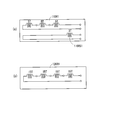
- (A) is a plan view of the right transmitting coil
- (b) is a plan view of the right receiving coil
- (c) is a plan view of the left transmitting coil
- (d) is a plan view of the left receiving coil.
- (A) is a circuit diagram of one division
- (b) is a circuit diagram of one division
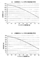
- (A) is a reception voltage characteristic diagram of the divided reception coil 120R1, and (b) is a reception voltage characteristic diagram of the division reception coil 120R2.
- FIG. 1 shows a sensor unit 100 of a metal strip end position measuring apparatus according to an embodiment of the present invention that measures the end position of a metal strip 300 conveyed in the direction of arrow A.
- 110R is a right transmitting coil
- 120R is a right receiving coil
- 110L is a left transmitting coil
- 120L is a left receiving coil.
- the right transmitting coil 110R and the right receiving coil 120R sandwich the right edge in the transport direction of the metal strip 300 from the plate thickness direction in a non-contact manner, and the direction perpendicular to the transport direction A of the metal strip 300 is the longitudinal direction.
- the left transmission coil 110L and the left reception coil 120L also sandwich the left edge of the metal strip 300 in the conveyance direction from the plate thickness direction in a non-contact manner, and the direction perpendicular to the conveyance direction A of the metal strip 300 is the longitudinal direction. Is arranged.
- FIGS. 2A to 2D show the configurations of the right transmitting coil 110R, the right receiving coil 120R, the left transmitting coil 110L, and the left receiving coil 120L.
- the right transmission coil 110R includes two divided transmission coils 110R1 and 110R2 each having a length L1 (for example, 570 mm) and a width W1 (for example, 30 mm) formed on the printed circuit board. These substrates are combined on the holder 111R so that the end length L2 (for example, 170 mm) is arranged side by side on the same plane, and the total length is set to the length L3 (for example, 800 mm).
- the right receiving coil 120R, the left transmitting coil 110L, and the left receiving coil 120L are similarly configured on the holders 121R, 111L, and 121L (FIGS. 2B, 2C, and 2D).
- the total length L3 of the right transmission coil 110R, the right reception coil 120R, the left transmission coil 110L, and the left reception coil 120L is set to an arbitrary length (for example, 1 m) by appropriately setting the length L2 adjacent to the length L1. (Length exceeding).
- segmentation reception coil 120R1 are made to oppose on the right side, and the division
- the divided transmission coils 110R1, 110R2, 110L1, and 110L2 are each composed of four layers of printed coil substrates.
- the split transmission coil 110R1 As shown in FIG. 3A, three identical substrates formed by photo-etching a coil having, for example, five turns are overlapped so that the coil portions overlap, The coils of each board are connected in series to make 15 turns. Further, a substrate having the same shape in which the reference coil 110RS1 having three turns is formed by photoetching is superimposed on the three-layer substrate so that the coil portions overlap each other. Thereby, the divided transmission coil 110R1 has a total of four layers of printed coil configuration.
- the divided receiving coils 120R1, 120R2, 120L1, and 120L2 are also each composed of a four-layer printed coil substrate.
- the divided receiving coil 120R1 will be described as a representative example.
- four identical substrates formed by photoetching a coil having, for example, 15 turns are overlapped so that the coil portions overlap each other.
- the substrate coils are connected in series to form 60 turns.
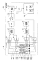
- FIG. 4 shows circuit blocks of the sensor unit 100 and the signal processing unit 200 of the metal strip end position measuring apparatus.
- the reference coils 110RS1, 110RS2, 110LS1, and 110LS2 are mounted on the divided transmission coils 110R1, 110R2, 110L1, and 110L2, respectively.
- the signal processing unit 200 includes a sine wave oscillator 201 that oscillates a high-frequency signal (for example, 80 kHz) that does not affect other devices and is not affected by the other devices, and a sine wave signal that is oscillated by the sine wave oscillator 201.
- a transmission signal amplifier 202 is provided.
- the high-frequency voltage amplified by the transmission signal amplifier 202 is repeatedly supplied in time division to the divided transmission coils 110R1, 110R2, 110L1, and 110L2 by switching the switch 203. Further, voltages induced in the reference coils 110RS1, 110RS2, 110LS1, and 110LS2 provided in the divided transmission coils 110R1, 110R2, 110L1, and 110L2 are captured in a time division manner by the switch 204 that switches in synchronization with the switch 203.
- the voltages induced in the divided reception coils 120R1, 120R2, 120L1, and 120L2 by the time division driving of the divided transmission coils 110R1, 110R2, 110L1, and 110L2 are switched by switches 205 and 206 that are switched in synchronization with the switches 203 and 204, respectively. It is repeatedly taken in time division and amplified by the high frequency amplifier 207.
- the voltage signal output from the high-frequency amplifier 207 is detected by the detection circuit 210 via the switch 209 after an unnecessary noise component is removed by the band pass filter 208, and becomes a DC component.
- the DC component is converted into a digital signal by the A / D converter 211 and taken into the microprocessor 212.
- the voltage induced in the reference coils 110RS1, 110RS2, 110LS1, and 110LS2 taken in a time division manner by the switch 204 is also selected by the switch 209, detected by the detection circuit 2011, and converted to a digital signal by the A / D converter 211. And taken into the microprocessor 212.
- the switch 209 selects the output of the switch 204 and the output of the band-pass filter 208 in a time-division manner during the period in which the switches 203 to 206 are selecting a specific terminal.
- the microprocessor 212 has a built-in storage device 212A for storing collected data or temporary data being processed, and a storage device 212B for storing a program for executing processing by the CPU.
- FIG. 5A and 5 (b) are tables for measuring the end position of the metal strip 300, and are stored in the storage device 212A in advance.
- FIG. 5A shows the characteristics of the received voltage obtained by processing the voltage induced in the divided receiving coil 12R1 inside the right receiving coil 120R. This characteristic is that as the area of the metal strip 300 located on the lower surface of the divided receiving coil 120R1 increases, that is, the amount of deviation from the line center of the end position of the metal strip 300 in the right direction in the conveyance direction (the center of the conveyance line). The distance between the metal strip 300 and the right end of the metal strip 300 increases, the metal strip 300 becomes an obstacle, and the received voltage decreases.
- FIG. 5B shows the voltage induced in the outer divided receiving coil 120R2, which also has the same characteristics.
- the measurement area is divided into 150 to 550 mm and 550 mm to 950 mm by the divided receiving coils 120R1 and 120R2. Yes.
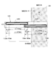
- FIG. 6 shows the relationship between the receiving coil 120R and the metal strip 300.
- the inner divided receiving coil 120R1 uses the range of the length L4 from the inner side of the length L1 (the right side in FIG. 6) as the effective measurement region, and uses the region of the length L2 adjacent to the outer divided receiving coil 120R2 as the measurement region. do not do.
- the table (FIG. 5 (a)) of the divided receiving coil 120R1 is created in the effective measurement area having the length L4.
- the outer divided receiving coil 120R2 also measures the range of the length L4 from the inside of the length L1 to the effective measurement region, and measures the region of the outer length L2 obtained by subtracting the inner length L4 from the length L1. Do not use as a region.
- the table (FIG. 5 (b)) of the divided receiving coil 120R2 is created in the effective measurement area having the length L4.
- the measurement region (length L2) of the overlapping portion of the divided receiving coils 120R1 and 120R2 is measured by the divided receiving coil 120R2.
- the split receiving coils 120R1 and 120R2 are arranged so that the end portions are arranged side by side, that is, so as not to overlap in the thickness direction, so that the magnetic coupling between them becomes small. For this reason, when the divided reception coil 120R1 detects the magnetic field generated by the divided transmission coil 110R1, it is less affected by the adjacent divided reception coil 120R2, and the measurement accuracy can be improved.
- receiving coil 120R of FIG. 6 is made to correspond to (a) and (b) of FIG. Is in the range of 550 mm to 950 mm.
- a similar effective measurement region is set for the divided reception coils 120L1 and 129L2 on the left side in the conveyance direction of the metal strip 300.
- FIG. 7A is a flowchart for selecting one of the right divided receiving coils 120R1 and 120R2
- FIG. 7B is a flowchart for selecting one of the left divided receiving coils 120L1 and 120L2.
- the program is stored in the storage device 212B and executed by the CPU in the microprocessor 212.
- the received voltage of the inner divided receiving coil 120R1 is a voltage in the effective measurement range (150 mm to 549 mm)
- the received voltage of the divided receiving coil 120R1 is adopted as the received voltage of the receiving coil 120R.
- the reception voltage of the outer divided reception coil 120R2 is adopted as the reception voltage of the reception coil 120R.
- the right end position of the metal strip 300 can be detected by the received voltage.
- the received voltage of the inner divided receiving coil 120L1 when the received voltage of the inner divided receiving coil 120L1 is in the effective measurement range (550 mm to 950 mm), the received voltage of the divided receiving coil 120L1 is adopted as the received voltage of the receiving coil 120L. Otherwise, the reception voltage of the outer divided reception coil 120L2 is adopted as the reception voltage of the reception coil 120L. Thereby, the left end position of the metal strip 300 can be detected by the received voltage.
- the intensity of the magnetic field generated in the transmission coils 110R and 110L is determined by the voltage output from the transmission signal amplifier 122.
- the voltage induced in the reception coils 120R and 120L by the magnetic field is determined by the coils, connection cables, and boards. Since it fluctuates depending on the temperature condition, the measurement result of the end position has a temperature characteristic.
- the voltage induced in the reference coils 110RS1, 110RS2, 110LS1, and 110LS2 mounted on the divided transmission coils 110R1, 110R2, 110L1, and 110L2 is set to a voltage that varies depending on the temperature, and is matched to the drive timing of the transmission coils. Capture.
- the microprocessor 212 corrects the voltage induced in the divided receiving coils 120R1, 120R2, 120L1, and 120L2 in accordance with the deviation from the reference value of the induced voltage (the value at the reference temperature). Thereby, the influence of the temperature drift on the measurement result of the end position of the metal strip 300 can be reduced (corrected), and the measurement error can be reduced.
- the number of divided transmission coils and the number of divided reception coils are two, but three or more may be used. As the number increases, the length L1 of the divided transmission coil and the divided reception coil can be shortened. Then, by adjusting the length L2 of the side-by-side region, it is possible to finely cope with the length required for the transmission coil and the reception coil.
- the transmission coil and the reception coil are arranged on both the left and right sides in the conveyance direction of the metal strip 300. However, the transmission coil and the reception coil are arranged so that the end position in the lateral direction of the metal strip 300 can be always measured. In this case, the transmission coil and the reception coil need only be arranged on one of the left and right sides of the metal strip 300.
Landscapes
- Physics & Mathematics (AREA)
- General Physics & Mathematics (AREA)
- Investigating Or Analyzing Materials By The Use Of Magnetic Means (AREA)
- Measurement Of Length, Angles, Or The Like Using Electric Or Magnetic Means (AREA)
Abstract
金属ストリップ300の側縁を板厚方向から非接触で挟み且つ前記搬送方向に直交する方向を長手方向が向くように配置される送信コイル110R及び受信コイル120Rを有するセンサ部100と、送信コイル110Rで発生した磁界が金属ストリップ300による電磁的影響を受けて受信コイル120Rに入力する際に誘起される電圧の大きさに応じて金属ストリップ300の端位置を計測する信号処理部200とを備え、送信コイル110Rは、2個の分割送信コイル110R1,110R2を隣り合う端部が同一平面上で横並びとなるような組み合わせで分割送信コイルよりも長く形成され、受信コイル120Rは、2個の分割受信コイル120R1,120R2を隣り合う端部が同一平面上で横並びとなるような組み合わせで分割受信コイルよりも長く形成され、分割送信コイル110R1と分割受信コイル120R1が対向し、分割送信コイル110R2と分割受信コイル120R2が対向した金属ストリップ端位置計測装置。
Description
本発明は、一定方向に搬送される所定幅の金属ストリップの少なくとも片側の端位置を計測する金属ストリップ端位置計測装置に関する。
この種の装置として、金属ストリップの搬送方向の右側端と左側端に、その金属ストリップを板厚方向から非接触で挟むように、一対の送信コイルと受信コイルを配置した装置がある(特許文献1、2)。
この装置では、送信コイルを駆動したとき、そこで発生した磁界が受信コイルに入力する際に、金属ストリップの側縁(端)による電磁的影響を受ける。そこで、このとき、受信コイルに誘起される電圧の大きさを判定することにより、金属ストリップの端位置を計測することができる。たとえば、右側の受信コイルにより計測される端位置がPRであり、左側の受信コイルにより計測される端位置がPLであるときは、その金属ストリップのラインセンタからの偏差(蛇行量)は、(PR-PL)/2で求められる。
このとき、送信コイルと受信コイルの金属ストリップの搬送方向に直交する方向のそれぞれの長さは、金属ストリップの最大幅の蛇行量をカバーできる長さである必要があり、通常、1m程度の長さが必要となる。
ところで、コイルは、その精度を確保する必要がある場合には、プリント基板上にフォトエッチングを利用して形成することが行われるが、上記のように1mに達するような長い送信コイルや受信コイルは、プリント基板上に形成することは製造上から非常に困難である。
そこで、特許文献2では、金属シートをレーザビームにより切り抜いて送信コイルや受信コイルを形成することで、長い送信コイルや受信コイルを実現する際の精度の確保を図っているが、その製造には大掛かりな装置が必要となっている。
本発明の目的は、短尺のプリント基板上に形成した送信コイルおよび受信コイルを使用しながらも、金属ストリップの端位置を正確に計測でき、且つ幅が異なる多種類の金属ストリップに対応できるようにした金属ストリップ端位置計測装置を提供することである。
上記目的を達成するために、請求項1にかかる発明の金属ストリップ端位置計測装置は、所定方向に搬送される所定幅の金属ストリップの少なくとも一方の端を前記金属ストリップの板厚方向から非接触で挟み且つ前記搬送の方向に対して直交する方向を長手方向が向くように配置される所定長の送信コイル及び受信コイルを有するセンサ部と、前記送信コイルで発生した磁界が前記金属ストリップによる電磁的影響を受けて前記受信コイルに入力する際の前記受信コイルに誘起される電圧の大きさに応じて前記金属ストリップの端位置を計測する信号処理部と、を備えた金属ストリップ端位置計測装置において、前記送信コイルは、互いに独立した基板上にプリントされた第1、第2、・・・、第N(N:2以上の整数)の分割送信コイルを隣り合う端部が同一平面上で横並びとなるように組み合わせて個々の前記分割送信コイルよりも長く形成され、前記受信コイルは、互いに独立した基板上にプリントされた第1、第2、・・・、第Nの分割受信コイルを隣り合う端部が同一平面上で横並びとなるように組み合わせて個々の前記分割受信コイルよりも長く形成され、前記第1の分割送信コイルと前記第1の分割受信コイル、前記第2の分割送信コイルと前記第2の分割受信コイル、・・・、前記第Nの分割送信コイルと前記第Nの分割受信コイルが、それぞれ対向している、ことを特徴とする。
請求項2にかかる発明は、請求項1に記載の金属ストリップ端位置計測装置において、前記第1、第2、・・・、第Nの分割送信コイルは順次時分割で繰り返し駆動され、前記信号処理部は、前記第1、第2、・・・、第Nの分割送信コイルの駆動に同期して前記第1、第2、・・・、第Nの分割受信コイルに誘起される電圧を順次取り込み、前記金属ストリップの前記端位置を計測することを特徴とする。
請求項3にかかる発明は、請求項1又は2に記載の金属ストリップ端位置計測装置において、前記信号処理部は、前記金属ストリップの端位置と前記第1、第2、・・・、第Nの分割受信コイルの誘起電圧との関係を示す第1、第2、・・・、第Nのテーブルを備え、該第1、第2、・・・、第Nのテーブルのうちの1つのテーブルの当該電圧に基づき前記端位置を計測することを特徴とする。
請求項4にかかる発明は、請求項1、2又は3に記載の金属ストリップ端位置計測装置において、前記第1、第2、・・・、第Nの分割送信コイルには、当該の第1、第2、・・・、第Nの分割送信コイルの駆動により電圧が誘起される第1、第2、・・・、第Nの基準コイルが、前記第1、第2、・・・、第Nの分割送信コイルと対の関係でそれぞれ搭載され、前記信号処理部は、前記第1、第2、・・・、第Nの基準コイルに誘起される電圧の大きさに応じて、前記第1、第2、・・・、第Nの受信コイルに誘起される電圧の温度補正を行うことを特徴とする。
本発明によれば、送信コイルは複数の分割送信コイルが隣り合う端部が同一平面上で横並びとなるような組み合わせで個々の分割送信コイルよりも長く形成され、受信コイルは複数の分割受信コイルが隣り合う端部が同一平面上で横並びとなるような組み合わせで個々の分割受信コイルよりも長く形成される。このとき、分割送信コイルや分割受信コイルは十分に短尺化できる。よって、それら分割送信コイルや分割受信コイルは、プリント基板上に通常のフォトエッチングにより容易に形成することができる。このため、分割送信コイルや分割受信コイルを組み合わせて送信コイルや受信コイルを長尺化しても、その精度の確保と製造の容易さの両方を実現できる。そして、その長尺化も任意長が可能となるので、幅が異なる多種類の金属ストリップの端位置検出に対応できるようになる。
また、隣接する分割受信コイルに厚み方向の重なりが生じることがないため、特定の分割送信コイルに対応した特定の分割受信コイルに誘起される電圧が、隣接する別の分割受信コイルによる影響を受けにくくなり、計測精度を向上させることができる。
また、個々の分割送信コイルにそれぞれ基準コイルを搭載して、特定の分割送信コイルを駆動した際に、対応する基準コイルに誘起される電圧の温度特性を利用して、該特定の分割受信コイルに誘起される電圧の温度による影響を補償することができる。
図1に矢印A方向に搬送される金属ストリップ300の端位置を計測する本発明の実施例の金属ストリップ端位置計測装置のセンサ部100を示す。
110Rは右側送信コイル、120Rは右側受信コイル、110Lは左側送信コイル、120Lは左側受信コイルである。右側送信コイル110Rと右側受信コイル120Rは、金属ストリップ300の搬送方向の右側縁を板厚方向から非接触で挟むように、且つ金属ストリップ300の搬送方向Aに直交する方向が長手方向となるように配置されている。左側送信コイル110Lと左側受信コイル120Lも、金属ストリップ300の搬送方向の左側縁を板厚方向から非接触で挟むように、且つ金属ストリップ300の搬送方向Aに直交する方向が長手方向となるように配置されている。
図2(a)~(d)に右側送信コイル110R、右側受信コイル120R、左側送信コイル110L、左側受信コイル120Lの構成を示す。図2(a)に示すように、右側送信コイル110Rは、プリント基板上に形成された長さL1(例えば570mm)、幅W1(例えば30mm)の2個の分割送信コイル110R1,110R2を、それぞれの基板が同一平面上で端部の長さL2(例えば170mm)が横並びとなるようにホルダ111R上で組み合わせて、全長を長さL3(例えば800mm)にしたものである。
右側受信コイル120R、左側送信コイル110L及び左側受信コイル120Lについても、ホルダ121R,111L,121L上において、それぞれ同様に構成されている(図2(b),(c),(d))。
右側送信コイル110R、右側受信コイル120R、左側送信コイル110L、左側受信コイル120Lの全長の長さL3は、長さL1と隣り合う長さL2を適宜設定することで、任意の長さ(例えば1mを超える長さ)に設定することができる。
そして、これら複数のコイルからなるセンサ部100を金属ストリップ300に対して配置するときは、右側においては、分割送信コイル110R1と分割受信コイル120R1を対向させ、分割送信コイル110R2と分割受信コイル120R2を対向させる。また、左側においても、分割送信コイル110L1と分割受信コイル120L1を対向させ、左側の分割送信コイル110L2と分割受信コイル120R2と対向させる。
分割送信コイル110R1,110R2,110L1,110L2は、それぞれ4層のプリントコイル基板から構成されている。分割送信コイル110R1を代表して説明すると、図3(a)のように、巻数が例えば5ターンのコイルをフォトエッチングで形成した3枚の同一の基板を、コイル部分が重なるように重畳し、各基板のコイルを直列接続して15ターンとしたものである。この3層基板に対しては、さらに、巻数が3ターンの基準コイル110RS1をフォトエッチングで形成した同一形状の基板が、コイル部分が重なるように重畳されている。これにより、分割送信コイル110R1は合計で4層のプリントコイル構成となっている。
分割受信コイル120R1,120R2,120L1,120L2も、それぞれ4層のプリントコイル基板から構成されている。分割受信コイル120R1を代表して説明すると、図3(b)のように、巻数が例えば15ターンのコイルをフォトエッチングで形成した4枚の同一の基板をコイル部分が重なるように重畳し、各基板のコイルを直列接続して60ターンとなっている。
図4に金属ストリップ端位置計測装置のセンサ部100と信号処理部200の回路ブロックを示す。センサ部100において、分割送信コイル110R1,110R2,110L1,110L2には、一部前記したように、それぞれ基準コイル110RS1,110RS2,110LS1,110LS2が搭載されている。
信号処理部200は、他の装置に影響を与えずまた他の装置から影響を受けない高周波信号(例えば、80kHz)を発振する正弦波発振器201と、その正弦波発振器201で発振した正弦波信号を増幅する送信信号増幅器202を備える。
送信信号増幅器202で増幅された高周波電圧は、スイッチ203の切り替えによって分割送信コイル110R1,110R2,110L1,110L2に時分割で繰り返し供給される。また、分割送信コイル110R1、110R2,110L1,110L2に装備された基準コイル110RS1、110RS2,110LS1,110LS2に誘起された電圧は、スイッチ203と同期して切り替わるスイッチ204によって時分割で取り込まれる。
分割送信コイル110R1、110R2,110L1,110L2が時分割駆動されることで分割受信コイル120R1,120R2,120L1,120L2に誘起された電圧は、スイッチ203,204と同期して切り替わるスイッチ205,206によって、時分割で繰り返し取り込まれ、高周波増幅器207で増幅される。
この高周波増幅器207から出力する電圧信号は、バンドパスフィルタ208で不要なノイズ成分が除去されてから、スイッチ209を経由して検波回路210で検波され、直流成分となる。その直流成分は、A/D変換器211でディジタル信号に変換され、マイクロプロセッサ212に取り込まれる。
なお、スイッチ204で時分割で取り込まれた基準コイル110RS1、110RS2,110LS1,110LS2に誘起する電圧も、スイッチ209によって選択され、検波回路2011で検波され、A/D変換器211でディジタル信号に変換され、マイクロプロセッサ212に取り込まれる。スイッチ209は、スイッチ203~206が特定の端子を選択している期間内に、スイッチ204の出力とバンドパスフィルタ208の出力を時分割で選択する。
マイクロプロセッサ212には、採取したデータを格納したり処理中の一時的データ等を格納する記憶装置212AとCPUでの処理を実行させるプログラム等を格納する記憶装置212Bが内蔵されている。
図5(a),(b)は、金属ストリップ300の端位置を計測するためのテーブルであり、予め前記した記憶装置212Aに格納されている。図5(a)は右側受信コイル120Rの内側の分割受信コイル12R1に誘起される電圧を処理した受信電圧の特性を示すものである。この特性は、その分割受信コイル120R1の下面に位置する金属ストリップ300の面積が大きくなるほど、つまり金属ストリップ300の搬送方向の右方向への端位置のラインセンタからの偏移量(搬送ラインのセンタと金属ストリップ300の右端との間の距離)が大きくなるほど、その金属ストリップ300が障害となって、その受信電圧は小さくなっている。図5(b)は外側の分割受信コイル120R2に誘起される電圧を示すもので、やはり同様の特性となっている。
図5(a),(b)に示すように、金属ストリップ300の右側での偏移量の計測では、分割受信コイル120R1,120R2によってその計測領域が150~550mmと550mm~950mmに分担されている。
図6に受信コイル120Rと金属ストリップ300との関係を示す。内側の分割受信コイル120R1は、長さL1の内側(図6の右側)から長さL4の範囲を有効計測領域とし、外側の分割受信コイル120R2と隣り合う長さL2の領域は計測領域として使用しない。分割受信コイル120R1のテーブル(図5(a))は、長さL4の有効計測領域で作成される。また、外側の分割受信コイル120R2も、長さL1の内の内側から長さL4の範囲を有効計測領域とし、長さL1から内側の長さL4を差し引いた外側の長さL2の領域は計測領域として使用しない。分割受信コイル120R2のテーブル(図5(b))は、長さL4の有効計測領域で作成される。
このように、分割受信コイル120R1と120R2の重なり部分の計測領域(長さL2)は、分割受信コイル120R2によって計測される。
なお、分割受信コイル120R1と120R2の配置は、端部が横並びとなるように、つまり厚み方向に重ならないように行われるので、それらの相互間の磁気的結合が小さくなる。このため、分割受信コイル120R1が分割送信コイル110R1で発生する磁界を検出するとき、隣の分割受信コイル120R2の影響を受けにくくなり、計測精度を向上させることができる。
図6の受信コイル120Rを前記した図5の(a),(b)に対応させれば、分割受信コイル120R1の有効計測領域L4は150mm~549mmの範囲、分割受信コイル120R2の有効計測領域L4は550mm~950mmの範囲となる。なお、金属ストリップ300の搬送方向の左側の分割受信コイル120L1,129L2についても、同様の有効計測領域が設定されている。
図7(a)は右側の分割受信コイル120R1と120R2の一方を選択処理するためのフローチャート、図7(b)は左側の分割受信コイル120L1と120L2の一方を選択処理するためのフローチャートであり、そのプログラムは記憶装置212Bに格納され、マイクロプロセッサ212内のCPUにより実行される。
図7(a)において、内側の分割受信コイル120R1の受信電圧が有効計測範囲(150mm~549mm)の電圧であるときは、その分割受信コイル120R1の受信電圧を受信コイル120Rの受信電圧として採用し、そうでないときは、外側の分割受信コイル120R2の受信電圧を受信コイル120Rの受信電圧として採用する。これにより、受信電圧によって金属ストリップ300の右側の端位置を検出することができる。
図7(b)において、内側の分割受信コイル120L1の受信電圧が有効計測範囲(550mm~950mm)の電圧であるときは、その分割受信コイル120L1の受信電圧を受信コイル120Lの受信電圧として採用し、そうでないときは、外側の分割受信コイル120L2の受信電圧を受信コイル120Lの受信電圧として採用する。これにより、受信電圧によって金属ストリップ300の左側の端位置を検出することができる。
ところで、送信コイル110R,110Lに発生する磁界の強度は、送信信号増幅器122から出力する電圧によって決まるが、その磁界によって受信コイル120R,120Lに誘起される電圧は、各コイル、接続ケーブルおよび基板の温度条件によって変動するので、端位置の計測結果が温度特性を持つようになり、このままでは計測誤差を招く。
そこで本実施例では、分割送信コイル110R1,110R2,110L1,110L2に搭載された基準コイル110RS1,110RS2,110LS1,110LS2に誘起する電圧を、温度によって変化する電圧として、それら送信コイルの駆動タイミングに合わせて取り込む。そして、その誘起電圧の基準値(基準温度時の値)からのズレに応じて、マイクロプロセッサ212において、分割受信コイル120R1,120R2,120L1,120L2に誘起された電圧の補正を行う。これによって、金属ストリップ300の端位置の計測結果の温度ドリフトによる影響を軽減(補正)することができ、計測誤差を軽減できる。
なお、以上では、分割送信コイルと分割受信コイルをそれぞれ2個としたが、3個以上にしてもよい。その個数が増えるほど、分割送信コイルや分割受信コイルの長さL1を短くできる。そして、横並び領域の長さL2を調整すれば、送信コイルや受信コイルに要求される長さに細かく対応することができる。また、以上の実施例では送信コイルと受信コイルを金属ストリップ300の搬送方向の左右両側に配置したが、金属ストリップ300の横方向への端位置を常時計測できるように送信コイルと受信コイルが配置されている場合には、送信コイルと受信コイルは金属ストリップ300の左右両側の一方の側にのみ配置すればよい。
100:センサ部
110R:右側送信コイル、110R1,110R2:分割送信コイル
110L:左側送信コイル、110L1,110L2:分割送信コイル
110RS1,110RS2,110LS1,110LS2:基準コイル
120R:右側受信コイル、120R1,120R2:分割受信コイル
120L:左側受信コイル、120L1,120L2:受信送信コイル
111R,121R,111L,121L:ホルダ
200:信号処理部、201:正弦波発振器、202:送信信号増幅器、203~206:スイッチ、207:高周波増幅器、208:バンドパスフィルタ、209:スイッチ、210:検波回路、211:A/D変換器、212:マイクロプロセッサ、212A,212B:記憶装置
110R:右側送信コイル、110R1,110R2:分割送信コイル
110L:左側送信コイル、110L1,110L2:分割送信コイル
110RS1,110RS2,110LS1,110LS2:基準コイル
120R:右側受信コイル、120R1,120R2:分割受信コイル
120L:左側受信コイル、120L1,120L2:受信送信コイル
111R,121R,111L,121L:ホルダ
200:信号処理部、201:正弦波発振器、202:送信信号増幅器、203~206:スイッチ、207:高周波増幅器、208:バンドパスフィルタ、209:スイッチ、210:検波回路、211:A/D変換器、212:マイクロプロセッサ、212A,212B:記憶装置
Claims (4)
- 所定方向に搬送される所定幅の金属ストリップの少なくとも一方の端を前記金属ストリップの板厚方向から非接触で挟み且つ前記搬送の方向に対して直交する方向を長手方向が向くように配置される所定長の送信コイル及び受信コイルを有するセンサ部と、前記送信コイルで発生した磁界が前記金属ストリップによる電磁的影響を受けて前記受信コイルに入力する際の前記受信コイルに誘起される電圧の大きさに応じて前記金属ストリップの端位置を計測する信号処理部と、を備えた金属ストリップ端位置計測装置において、
前記送信コイルは、互いに独立した基板上にプリントされた第1、第2、・・・、第N(N:2以上の整数)の分割送信コイルを隣り合う端部が同一平面上で横並びとなるように組み合わせて個々の前記分割送信コイルよりも長く形成され、
前記受信コイルは、互いに独立した基板上にプリントされた第1、第2、・・・、第Nの分割受信コイルを隣り合う端部が同一平面上で横並びとなるように組み合わせて個々の前記分割受信コイルよりも長く形成され、
前記第1の分割送信コイルと前記第1の分割受信コイル、前記第2の分割送信コイルと前記第2の分割受信コイル、・・・、前記第Nの分割送信コイルと前記第Nの分割受信コイルが、それぞれ対向している、
ことを特徴とする金属ストリップ端位置計測装置。 - 請求項1に記載の金属ストリップ端位置計測装置において、
前記第1、第2、・・・、第Nの分割送信コイルは順次時分割で繰り返し駆動され、
前記信号処理部は、前記第1、第2、・・・、第Nの分割送信コイルの駆動に同期して前記第1、第2、・・・、第Nの分割受信コイルに誘起される電圧を順次取り込み、前記金属ストリップの前記端位置を計測することを特徴とする金属ストリップ端位置計測装置。 - 請求項1又は2に記載の金属ストリップ端位置計測装置において、
前記信号処理部は、前記金属ストリップの端位置と前記第1、第2、・・・、第Nの分割受信コイルの誘起電圧との関係を示す第1、第2、・・・、第Nのテーブルを備え、該第1、第2、・・・、第Nのテーブルのうちの1つのテーブルの当該電圧に基づき前記端位置を計測することを特徴とする金属ストリップ端位置計測装置。 - 請求項1、2又は3に記載の金属ストリップ端位置計測装置において、
前記第1、第2、・・・、第Nの分割送信コイルには、当該の第1、第2、・・・、第Nの分割送信コイルの駆動により電圧が誘起される第1、第2、・・・、第Nの基準コイルが、前記第1、第2、・・・、第Nの分割送信コイルと対の関係でそれぞれ搭載され、
前記信号処理部は、前記第1、第2、・・・、第Nの基準コイルに誘起される電圧の大きさに応じて、前記第1、第2、・・・、第Nの受信コイルに誘起される電圧の温度補正を行うことを特徴とする金属ストリップ端位置計測装置。
Priority Applications (1)
| Application Number | Priority Date | Filing Date | Title |
|---|---|---|---|
| PCT/JP2014/068922 WO2016009509A1 (ja) | 2014-07-16 | 2014-07-16 | 金属ストリップ端位置計測装置 |
Applications Claiming Priority (1)
| Application Number | Priority Date | Filing Date | Title |
|---|---|---|---|
| PCT/JP2014/068922 WO2016009509A1 (ja) | 2014-07-16 | 2014-07-16 | 金属ストリップ端位置計測装置 |
Publications (1)
| Publication Number | Publication Date |
|---|---|
| WO2016009509A1 true WO2016009509A1 (ja) | 2016-01-21 |
Family
ID=55078028
Family Applications (1)
| Application Number | Title | Priority Date | Filing Date |
|---|---|---|---|
| PCT/JP2014/068922 Ceased WO2016009509A1 (ja) | 2014-07-16 | 2014-07-16 | 金属ストリップ端位置計測装置 |
Country Status (1)
| Country | Link |
|---|---|
| WO (1) | WO2016009509A1 (ja) |
Cited By (1)
| Publication number | Priority date | Publication date | Assignee | Title |
|---|---|---|---|---|
| CN114061422A (zh) * | 2020-07-31 | 2022-02-18 | Emg自动化有限公司 | 用于感应地测量金属带的边缘定位的装置 |
Citations (5)
| Publication number | Priority date | Publication date | Assignee | Title |
|---|---|---|---|---|
| JPS53133055A (en) * | 1977-04-26 | 1978-11-20 | Nippon Steel Corp | Width detecting method for magnetic metal strips |
| JPH07181002A (ja) * | 1991-08-14 | 1995-07-18 | Elmeg Elektro Mechanik Gmbh | 金属ストリップ位置の誘電測定方法とその装置 |
| JP2000035307A (ja) * | 1998-03-24 | 2000-02-02 | Elektro-Mechanik Gmbh | 金属ストリップの誘導的位置測定装置 |
| JP2005114625A (ja) * | 2003-10-09 | 2005-04-28 | Nireco Corp | 磁性体縁辺位置検出装置 |
| JP2010533847A (ja) * | 2007-07-19 | 2010-10-28 | ツェットエフ フリードリヒスハーフェン アクチエンゲゼルシャフト | 局所的な測定範囲におけるコイル配置構造 |
-
2014
- 2014-07-16 WO PCT/JP2014/068922 patent/WO2016009509A1/ja not_active Ceased
Patent Citations (5)
| Publication number | Priority date | Publication date | Assignee | Title |
|---|---|---|---|---|
| JPS53133055A (en) * | 1977-04-26 | 1978-11-20 | Nippon Steel Corp | Width detecting method for magnetic metal strips |
| JPH07181002A (ja) * | 1991-08-14 | 1995-07-18 | Elmeg Elektro Mechanik Gmbh | 金属ストリップ位置の誘電測定方法とその装置 |
| JP2000035307A (ja) * | 1998-03-24 | 2000-02-02 | Elektro-Mechanik Gmbh | 金属ストリップの誘導的位置測定装置 |
| JP2005114625A (ja) * | 2003-10-09 | 2005-04-28 | Nireco Corp | 磁性体縁辺位置検出装置 |
| JP2010533847A (ja) * | 2007-07-19 | 2010-10-28 | ツェットエフ フリードリヒスハーフェン アクチエンゲゼルシャフト | 局所的な測定範囲におけるコイル配置構造 |
Cited By (1)
| Publication number | Priority date | Publication date | Assignee | Title |
|---|---|---|---|---|
| CN114061422A (zh) * | 2020-07-31 | 2022-02-18 | Emg自动化有限公司 | 用于感应地测量金属带的边缘定位的装置 |
Similar Documents
| Publication | Publication Date | Title |
|---|---|---|
| US9228823B2 (en) | Inductive position sensor | |
| JP6166227B2 (ja) | 送電装置及び受電装置 | |
| KR102331508B1 (ko) | 위치 지시기 및 그 제조 방법 | |
| TWI556693B (zh) | 包含一電容感測器之一電極組態之印刷電路板 | |
| US8860436B2 (en) | Sensor of electromagnetic induction type coordinate input device | |
| US7654009B2 (en) | Absolute value scale and absolute value calculating method | |
| JP2017514452A5 (ja) | ||
| JP6115608B2 (ja) | 高周波フィルタ、および通信機器モジュール | |
| JP6471647B2 (ja) | 電極製造方法および電極製造装置 | |
| JP2019062182A (ja) | コイル部品 | |
| JP4437156B2 (ja) | 金属製物体の位置を検出する検出器 | |
| WO2017033722A1 (ja) | アンテナ装置 | |
| JP6048700B2 (ja) | 方向性結合器および無線通信装置 | |
| US9714147B2 (en) | Sheet processing apparatus and method of detecting thickness of sheet | |
| US20170006667A1 (en) | Cooking appliance | |
| JP2016217947A (ja) | 金属検出機 | |
| JP4442945B2 (ja) | 金属ストリップの誘導的位置測定装置 | |
| EP1744182B1 (en) | Magnetic material detecting apparatus | |
| US20220229094A1 (en) | Magnetic sensor and current detecting apparatus including the same | |
| JP7267037B2 (ja) | 磁気検出装置及び硬貨識別装置 | |
| JP5609398B2 (ja) | 磁界プローブ | |
| JP2013120110A (ja) | 磁界プローブ | |
| CN105814653B (zh) | 多件同时加工印刷布线板和线圈图案的检查方法 | |
| JP5609328B2 (ja) | 磁界プローブ | |
| JP2009089148A (ja) | プリント配線板 |
Legal Events
| Date | Code | Title | Description |
|---|---|---|---|
| 121 | Ep: the epo has been informed by wipo that ep was designated in this application |
Ref document number: 14897573 Country of ref document: EP Kind code of ref document: A1 |
|
| NENP | Non-entry into the national phase |
Ref country code: DE |
|
| 122 | Ep: pct application non-entry in european phase |
Ref document number: 14897573 Country of ref document: EP Kind code of ref document: A1 |
|
| NENP | Non-entry into the national phase |
Ref country code: JP |