WO2016010053A1 - Élément électrique - Google Patents
Élément électrique Download PDFInfo
- Publication number
- WO2016010053A1 WO2016010053A1 PCT/JP2015/070205 JP2015070205W WO2016010053A1 WO 2016010053 A1 WO2016010053 A1 WO 2016010053A1 JP 2015070205 W JP2015070205 W JP 2015070205W WO 2016010053 A1 WO2016010053 A1 WO 2016010053A1
- Authority
- WO
- WIPO (PCT)
- Prior art keywords
- thin film
- terminal
- conductor layer
- base material
- layer
- Prior art date
- Legal status (The legal status is an assumption and is not a legal conclusion. Google has not performed a legal analysis and makes no representation as to the accuracy of the status listed.)
- Ceased
Links
Images


Classifications
-
- B—PERFORMING OPERATIONS; TRANSPORTING
- B32—LAYERED PRODUCTS
- B32B—LAYERED PRODUCTS, i.e. PRODUCTS BUILT-UP OF STRATA OF FLAT OR NON-FLAT, e.g. CELLULAR OR HONEYCOMB, FORM
- B32B9/00—Layered products comprising a layer of a particular substance not covered by groups B32B11/00 - B32B29/00
-
- C—CHEMISTRY; METALLURGY
- C25—ELECTROLYTIC OR ELECTROPHORETIC PROCESSES; APPARATUS THEREFOR
- C25D—PROCESSES FOR THE ELECTROLYTIC OR ELECTROPHORETIC PRODUCTION OF COATINGS; ELECTROFORMING; APPARATUS THEREFOR
- C25D7/00—Electroplating characterised by the article coated
-
- C—CHEMISTRY; METALLURGY
- C23—COATING METALLIC MATERIAL; COATING MATERIAL WITH METALLIC MATERIAL; CHEMICAL SURFACE TREATMENT; DIFFUSION TREATMENT OF METALLIC MATERIAL; COATING BY VACUUM EVAPORATION, BY SPUTTERING, BY ION IMPLANTATION OR BY CHEMICAL VAPOUR DEPOSITION, IN GENERAL; INHIBITING CORROSION OF METALLIC MATERIAL OR INCRUSTATION IN GENERAL
- C23C—COATING METALLIC MATERIAL; COATING MATERIAL WITH METALLIC MATERIAL; SURFACE TREATMENT OF METALLIC MATERIAL BY DIFFUSION INTO THE SURFACE, BY CHEMICAL CONVERSION OR SUBSTITUTION; COATING BY VACUUM EVAPORATION, BY SPUTTERING, BY ION IMPLANTATION OR BY CHEMICAL VAPOUR DEPOSITION, IN GENERAL
- C23C18/00—Chemical coating by decomposition of either liquid compounds or solutions of the coating forming compounds, without leaving reaction products of surface material in the coating; Contact plating
- C23C18/02—Chemical coating by decomposition of either liquid compounds or solutions of the coating forming compounds, without leaving reaction products of surface material in the coating; Contact plating by thermal decomposition
- C23C18/12—Chemical coating by decomposition of either liquid compounds or solutions of the coating forming compounds, without leaving reaction products of surface material in the coating; Contact plating by thermal decomposition characterised by the deposition of inorganic material other than metallic material
-
- C—CHEMISTRY; METALLURGY
- C23—COATING METALLIC MATERIAL; COATING MATERIAL WITH METALLIC MATERIAL; CHEMICAL SURFACE TREATMENT; DIFFUSION TREATMENT OF METALLIC MATERIAL; COATING BY VACUUM EVAPORATION, BY SPUTTERING, BY ION IMPLANTATION OR BY CHEMICAL VAPOUR DEPOSITION, IN GENERAL; INHIBITING CORROSION OF METALLIC MATERIAL OR INCRUSTATION IN GENERAL
- C23C—COATING METALLIC MATERIAL; COATING MATERIAL WITH METALLIC MATERIAL; SURFACE TREATMENT OF METALLIC MATERIAL BY DIFFUSION INTO THE SURFACE, BY CHEMICAL CONVERSION OR SUBSTITUTION; COATING BY VACUUM EVAPORATION, BY SPUTTERING, BY ION IMPLANTATION OR BY CHEMICAL VAPOUR DEPOSITION, IN GENERAL
- C23C28/00—Coating for obtaining at least two superposed coatings either by methods not provided for in a single one of groups C23C2/00 - C23C26/00 or by combinations of methods provided for in subclasses C23C and C25C or C25D
-
- H—ELECTRICITY
- H01—ELECTRIC ELEMENTS
- H01H—ELECTRIC SWITCHES; RELAYS; SELECTORS; EMERGENCY PROTECTIVE DEVICES
- H01H1/00—Contacts
- H01H1/02—Contacts characterised by the material thereof
- H01H1/04—Co-operating contacts of different material
-
- H—ELECTRICITY
- H01—ELECTRIC ELEMENTS
- H01R—ELECTRICALLY-CONDUCTIVE CONNECTIONS; STRUCTURAL ASSOCIATIONS OF A PLURALITY OF MUTUALLY-INSULATED ELECTRICAL CONNECTING ELEMENTS; COUPLING DEVICES; CURRENT COLLECTORS
- H01R13/00—Details of coupling devices of the kinds covered by groups H01R12/70 or H01R24/00 - H01R33/00
- H01R13/02—Contact members
- H01R13/03—Contact members characterised by the material, e.g. plating, or coating materials
Definitions
- the present invention relates to an electrical element useful as an electrical contact for a connector.
- the electrical contact for a connector is mainly formed of a Cu alloy.
- the Cu alloy is used as it is, there is a problem in that the surface is oxidized, the electrical resistivity is increased, and the reliability of the product is lowered.
- a small and low contact load electrical contact has a problem in that the contact surface between the metal parts at the contact portion (true contact surface) becomes very small due to the high resistance oxide film, and the contact resistance increases. .
- noble metal plating such as gold or silver is formed on the surface of the Cu alloy to form a noble metal plating layer, thereby preventing the oxidation of the surface of the Cu alloy and ensuring the reliability of the product.
- the noble metal plating layer is provided with a certain thickness. Apart from this, even when used at a relatively large current of several tens to several hundred amperes, such as those used for charging storage batteries of electric vehicles, it is necessary to increase the thickness of the noble metal plating layer.
- Patent Document 1 a metal layer made of, for example, Sn is formed on a base material, an oxide layer formed on the surface thereof is removed, and then an oxide layer such as SnO 2 is formed on the metal layer.
- a method of manufacturing an electrical contact material for a connector to be formed is disclosed.
- the object of the present invention is low cost, prevents deterioration of product reliability due to oxidation of the base material, and keeps the true contact surface large even for a small and low contact load electrical contact. It is an object of the present invention to provide an electrical element that can solve the problem of increased contact resistance.
- the present inventor has found that the above problem can be solved by providing a specific oxide thin film on a base material, and has completed the present invention. That is, the present invention is characterized by the following (1) to (8).
- the electric element according to (1), wherein the element is an element that contributes to the development of conductivity.
- the electric element according to (2), wherein the element contributing to conductivity is at least one selected from the group consisting of F, In, Ga, Tl, As, Sb, and Bi.
- the electric element according to (2), wherein the element contributing to the development of conductivity is F.
- the electric element according to any one of (1) to (5), wherein a surface of the base material is plated with a noble metal.
- the electrical element of the present invention is provided with a specific oxide thin film on a base material, it is low in cost and prevents deterioration of product reliability due to oxidation of the base material, and is small and has a low contact load. Even in the case of the electrical contact, it is possible to provide an electrical element capable of maintaining a large true contact surface and solving the problem of an increase in contact resistance. In addition, the electric element of the present invention can effectively prevent discoloration of Ag during actual use even when the surface of the base material is plated with Ag, and improve the reliability of the electric element. Can do.
- FIG. 1 is a cross-sectional view for explaining an electric element according to the first embodiment of the present invention.
- FIG. 2 is a cross-sectional view for explaining the connector electrical contact according to the first embodiment of the present invention.
- Fig.3 (a) is sectional drawing of the electrical contact 3 for connectors manufactured in the Example of 1st Embodiment,
- FIG.3 (b) is a partially expanded view.
- FIG. 4A is a plan view of a plate-like conductor according to the second embodiment of the present invention
- FIG. 4B is a cross-sectional view taken along line BB in FIG. 4A.
- FIG.5 (a) is a top view which shows the lamination
- FIG.5 (b) is a figure. It is CC sectional drawing of 5 (a).
- FIG. 6 is a schematic diagram for explaining an electric element provided with the oxide thin film according to the third embodiment.
- FIG. 7 is a cross-sectional view of a terminal according to the third embodiment of the present invention.
- FIG. 8 is a partially enlarged view of FIG.
- FIG. 9 is a cross-sectional view for explaining an electric element provided with an oxide thin film according to the fourth embodiment of the present invention.
- FIG. 6 is a schematic diagram for explaining an electric element provided with the oxide thin film according to the third embodiment.
- FIG. 7 is a cross-sectional view of a terminal according to the third embodiment of the present invention.
- FIG. 8 is a partially enlarged view of FIG.
- FIG. 10 is a schematic diagram of a terminal according to the fourth embodiment of the present invention.
- FIG. 11 is a top view in the contact part of the terminal which concerns on 4th Embodiment of this invention.
- FIG. 12 is a cross-sectional view of the contact portion of the terminal according to the fourth embodiment of the present invention.
- FIG. 13 is a longitudinal sectional view of a terminal fitting according to a fifth embodiment of the present invention.
- FIG. 14 is an enlarged view of a portion A in FIG.
- FIG. 15 is a longitudinal sectional view of another example of the plating material according to the fifth embodiment of the present invention.
- FIG. 1 is a cross-sectional view for explaining an electric element according to the first embodiment of the present invention.
- the electric element 1 shown in FIG. 1 is formed by providing an oxide thin film 16 doped with an element on a base 12.
- the material of the substrate 12 is not particularly limited and can be appropriately selected depending on the application.
- the material of the oxide thin film 16 is not particularly limited and can be appropriately selected depending on the application. Moreover, it does not restrict
- the manufacturing method of the electric element 1 is not particularly limited, and a conventionally known method can be appropriately employed.
- FIG. 2 is a cross-sectional view for explaining the connector electrical contact according to the present embodiment.
- the connector electrical contact 2 is provided with a Ni plating layer 132, a noble metal plating layer 142, and an oxide thin film 162 in this order on a substrate 122.
- another plating layer may be provided in order to improve the adhesion between the Ni plating layer 132 and the noble metal plating layer 142.
- the material of the base material 122 can generally be a Cu alloy such as Cu or brass. Apart from this, Al, Fe or alloys thereof can also be used.
- the thickness of the base material 122 can be appropriately determined according to the application, and the shape of the base material can be a rectangular shape, a cylindrical shape, or other irregular shapes.
- a Ni plating layer 132 may be provided on the base material 122 in order to prevent, for example, Cu or Cu alloy contained in the base material 122 from diffusing on the oxide thin film 162.
- the Ni plating layer 132 can be made of Ni or an Ni alloy such as an Fe—Ni alloy or an Sn—Ni alloy. The thickness of the Ni plating layer 132 is determined as appropriate as long as the object can be achieved.
- a noble metal plating layer 142 is provided on the surface of the Ni plating layer 132.
- the noble metal in the noble metal plating layer 142 include Au and Ag.
- the thickness of the noble metal plating layer 142 may be appropriately determined in consideration of the use and cost.
- an oxide thin film 162 doped with an element is provided on the noble metal plating layer 142.
- the oxide include SnO, SnO 2 , NiO, Ni 2 O 3 , ZnO, CuO 2 , CuAlO 2 , In 2 O 3 , or a mixture thereof. From the viewpoint of inter alia improving the effect of the present invention, the oxide is preferably a SnO and / or SnO 2.
- the element is preferably an element that contributes to the development of conductivity, and includes, for example, at least one selected from the group consisting of F, In, Ga, Tl, As, Sb, and Bi.
- F is preferable, and the oxide thin film 162 is particularly preferably fluorine-doped tin oxide (FTO).
- the thickness of the oxide thin film 162 is, for example, 10 nm to 1 ⁇ m.
- the base material 122 is prepared, and the Ni plating layer 132 and the noble metal plating layer 142 are sequentially formed as necessary.
- Each plating layer can be formed by a known plating method.
- the electrolytic plating method is a method that is conventionally performed, and is preferable because the apparatus configuration is simple and the control of the layer thickness is relatively easy.
- an oxide thin film 162 doped with an element is provided on the noble metal plating layer 142.
- the oxide thin film 162 can be provided by, for example, a spray pyrolysis (SPD: Spray Pyrolysis Deposition) method.
- SPD Spray Pyrolysis Deposition
- the substrate is heated to the film formation temperature and sprayed with the solution that is the raw material of the film using a spraying means such as an atomizer toward the initial stage.
- a spraying means such as an atomizer toward the initial stage.
- Forms a crystal by evaporating the solvent in the droplets attached to the substrate surface, followed by the hydrolysis and thermal oxidation reactions following the thermal decomposition of the solute, and as the reaction proceeds, the droplets form on the crystals.
- the oxide thin film 162 can be formed in a pinpoint and / or arbitrary shape. Note that the oxide thin film 162 can be formed by a known method other than the SPD method.
- the oxide thin film 162 formed in this manner has conductivity (for example, a specific resistance value of 1 ⁇ 10 7 ⁇ ⁇ cm or less), exhibits the effects of the present invention, and wear resistance. Excellent in corrosion resistance, corrosion resistance, heat resistance, etc. Therefore, the thickness of the noble metal plating layer 142 provided in the lower layer can be reduced, which can contribute to a reduction in manufacturing cost.
- the present invention has been described by taking the connector electrical contact 2 as an example of the electrical element 1 of the present invention. However, in addition to this application, it can be used for various applications as an electrical element known in the art. .
- FIG. 3 is a cross-sectional view (a) and a partially enlarged view (b) of the connector electrical contact 3 manufactured in the present embodiment.
- the connector electrical contact 3 includes a male terminal 32 and a female terminal 34, and the fitting portion thereof is a male as shown in a partially enlarged view of FIG. 3 (b).
- the terminal 32 side is sequentially formed from the base material 182, the Ag plating layer 184 and the FTO thin film 186, and is in contact with the FTO thin film 196 on the female terminal 34 side.
- the female terminal 34 has the same configuration as the male terminal 32. That is, the female terminal 34 has a base material 182 and an Ag plating layer 194.
- a Cu alloy made of brass was used as the substrate 182, and an Ag plating layer 184 was formed thereon by an electrolytic plating method. Then, the FTO thin film 186 was provided on the Ag plating layer 184 by the SPD method, and the male terminal 32 was manufactured.
- the material of the base material of the male terminal 32 and the female terminal 34 may differ from each other.
- the connector electrical contact 3 of this embodiment can reduce the amount of Ag used in each stage in order to ensure the same performance as this, and at a low cost. In addition, it is possible to prevent a decrease in product reliability due to oxidation of the Cu alloy. Further, even if the connector electrical contact 3 is a small and low contact load electrical contact, the true contact surface can be kept large, and the problem of increased contact resistance can be solved. Furthermore, Ag discoloration during actual use can be effectively prevented.
- FIG. 4 shows a plate-like conductor according to the second embodiment of the present invention.
- FIG. 4A is a plan view of the plate-like conductor according to the second embodiment of the present invention
- FIG. ) Is a cross-sectional view taken along the line BB of FIG. 4A
- FIG. 5A is a plan view showing a laminated state of the first conductor layer and the second conductor layer in the plate-like conductor of the second embodiment of the present invention.
- FIG. 5 and FIG. 5B are CC cross-sectional views of FIG.
- the plate-like conductor 202 according to the second embodiment is formed in a plate shape having a predetermined thickness using a conductive material.
- the plate-like conductor 202 is used, for example, for a terminal fitting housed in a connector or a conductor pattern for a sliding contact formed on an insulating substrate.
- the plate-like conductor 202 of the present embodiment includes a first conductor layer 203, a second conductor layer 204, and a third conductor layer 205 as shown in FIG.
- the first conductor layer 203 is a conductor layer formed in a thin plate shape with a constant thickness by an inexpensive conductive material having lower conductivity and corrosion resistance than gold and silver.
- the first conductor layer 203 includes a base conductor layer 231 formed in a film shape with copper or a copper alloy, and a base conductor layer 232 formed to be laminated over the entire area of the base conductor layer 231. Thus, it is formed in a two-layer structure.
- the underlying conductor layer 232 is formed of nickel or a nickel alloy that facilitates the formation of the second conductor layer 204 formed thereon.
- the surface of the underlying conductor layer 232 is smooth.
- the second conductor layer 204 is formed in a film shape by partial plating on a part of the surface of the first conductor layer with gold or silver.
- the second conductor layer 204 has a rectangular shape with a predetermined film thickness t1, and is formed on the surface of the underlying conductor layer 232 with a certain interval P1, P2 vertically and horizontally. It is formed at intervals.
- the film thickness t1 of the second conductor layer 204 is set to 0.1 ⁇ m or less.
- the third conductor layer 205 covers the surface 203a of the first conductor layer 203 that is not equipped with the second conductor layer 204 and the surface 204a of the second conductor layer 204, and also the second conductor layer 204.
- a smooth surface 205a having no irregularities is formed by filling the recesses around the surface.
- the third conductor layer 205 is fluorine-doped tin oxide (FTO), and is formed so as to cover the surface 203a of the first conductor layer 203 and the surface 204a of the second conductor layer 204. Has been.
- FTO fluorine-doped tin oxide
- the 3rd conductor layer 205 which consists of fluorine dope tin oxide, it can provide by the spray thermal decomposition (SPD: Spray
- SPD spray thermal decomposition
- the substrate is heated to the film formation temperature and sprayed with the solution that is the raw material of the film using a spraying means such as an atomizer toward the initial stage.
- a spraying means such as an atomizer toward the initial stage.
- the fluorine-doped tin oxide can be formed by employing a known method other than the SPD method.
- Fluorine-doped tin oxide has a lower material cost than gold or silver.
- the fluorine-doped tin oxide film has a volume resistivity that is within an order of magnitude compared to the pure metal of tin (Sn), and is superior to gold and silver. It has conductivity.
- fluorine-doped tin oxide has low conductivity temperature dependency, excellent corrosion resistance and wear resistance, and exhibits excellent durability.
- the fluorine-doped tin oxide forming the third conductor layer 205 has excellent load resistance characteristics in which the resistance value is approximately an order of magnitude difference (1 order difference) compared to Ag plating, and has excellent conductivity. Demonstrate durability.
- the third conductor layer 205 that is the outermost layer and that is in contact with a contact point of an external device or the like is formed of fluorine-doped tin oxide.
- Fluorine-doped tin oxide has excellent corrosion resistance and conductivity as compared with copper, nickel, or alloys of these metals.
- the third conductor layer 205 made of fluorine-doped tin oxide is formed on the second conductor layer 204 formed of gold or silver having excellent corrosion resistance and conductivity. Therefore, it is possible to ensure extremely excellent corrosion resistance and conductivity as the entire conductor layer.
- the fluorine-doped tin oxide forming the third conductor layer 205 has excellent wear resistance compared to gold or silver, and the material cost is higher than that of gold or silver. , Low price.
- the second conductor layer 204 is formed of expensive gold or silver, but is used only in a part of the region by partial plating. Alternatively, the amount of silver used can be reduced to suppress an increase in manufacturing cost.
- the plate-shaped conductor of the second embodiment it is possible to ensure excellent corrosion resistance, conductivity and wear resistance, and to reduce the cost.
- the gold or silver forming the second conductor layer 204 is made of gold or silver having a high material cost by making the film thickness 0.1 ⁇ m or less. The amount of use can be reduced, and the reduction in manufacturing cost can be promoted.
- the first conductor layer 203 serving as the base part of the conductor through which an electric current flows is composed of a base conductor layer 231 made of copper or a copper alloy and the base conductor layer 231. It is a composite structure with a base conductor layer 232 made of nickel or a nickel alloy laminated thereon. The nickel or nickel alloy constituting the base conductor layer 232 is unlikely to form an oxide film, and the second conductor layer 204 and the third conductor layer 205 stacked on the base conductor layer 232 are formed.
- the third conductor layer 205 can be stably provided with excellent conductive performance, corrosion resistance, and wear resistance. be able to. Therefore, the reliability of various performances of the plate-like conductor 202 can be improved.
- the first conductor layer has a two-layer structure of the basic conductor layer and the base conductor layer, but the first conductor layer has a single layer structure of nickel alloy or copper alloy. Is also possible.
- FIG. 6 is a schematic view showing a cross section of an electric element provided with an oxide thin film.
- the electric element 301 is formed by providing an oxide thin film 316 doped with an element on a base material 312.
- the material of the base material 312 is not particularly limited and can be appropriately selected according to the use. However, as a connector terminal, a Cu alloy such as Cu or brass can be generally used. Apart from this, Al, Fe or alloys thereof can also be used.
- the thickness of the base material 312 can be appropriately determined according to the application, and the shape of the base material 312 can be a rectangular shape, a cylindrical shape, or other irregular shapes.
- the male terminal 332 and the female terminal 334 are formed using the base material 312.
- Examples of the material of the oxide constituting the oxide thin film 316 include SnO, SnO 2 , NiO, Ni 2 O 3 , ZnO, CuO 2 , CuAlO 2 , In 2 O 3 , or a mixture thereof. From the viewpoint of inter alia improving the effect of the present invention, the oxide is preferably a SnO and / or SnO 2.
- the element doped in the oxide thin film 316 is preferably an element that contributes to the development of conductivity, and includes, for example, at least one selected from the group consisting of F, In, Ga, Tl, As, Sb, and Bi.
- F is preferable
- the oxide thin film 316 is particularly preferably fluorine-doped tin oxide (FTO).
- the thickness of the oxide thin film 316 is, for example, 10 nm to 1 ⁇ m.
- a Ni plating layer may be provided on the base material 312 in order to prevent, for example, Cu or Cu alloy contained in the base material 312 from diffusing on the oxide thin film 316.
- Ni alloy such as Fe—Ni alloy and Sn—Ni alloy can be used in addition to Ni.
- the thickness of the Ni plating layer is determined as appropriate as long as the object can be achieved.
- the base material 312 is prepared, and the surface of a region where an FTO thin film 336 (described later) as the oxide thin film 316 is provided is polished. Polishing is performed by a known method for smoothing the surface, such as mechanical polishing or chemical polishing. Moreover, a Ni plating layer is formed on the surface of the base material 312 as necessary.
- the Ni plating layer can be formed by a method that keeps the surface smooth, such as a known plating method.
- the electrolytic plating method is a method that is conventionally performed, and is preferable because the apparatus configuration is simple and the control of the layer thickness is relatively easy.
- an oxide thin film 316 doped with an element is provided on the substrate 312.
- the oxide thin film 316 can be provided by, for example, a spray pyrolysis (SPD) method.
- SPD spray pyrolysis
- the substrate 312 is heated to a film formation temperature, and a solution as a film raw material is sprayed toward the substrate 312 using a spraying means such as an atomizer.
- a crystal is formed by the evaporation of the solvent in the droplet attached to the substrate surface and the hydrolysis reaction and thermal oxidation reaction following the thermal decomposition of the solute, and as the reaction proceeds, a droplet is formed on the crystal.
- the oxide thin film 316 can be formed in a pinpoint and / or arbitrary shape. Note that the oxide thin film 316 can be formed by a known method other than the SPD method.
- the oxide thin film 316 formed in this way has conductivity (for example, a specific resistance value of 1 ⁇ 10 7 ⁇ ⁇ cm or less), exhibits the above-described effects of the present invention, and wear resistance. Excellent in corrosion resistance, corrosion resistance, heat resistance, etc.
- FIG. 7 is a cross-sectional view of a terminal according to the third embodiment of the present invention.
- FIG. 8 is a partially enlarged view of the terminal shown in FIG.
- the male terminal 332 and the female terminal 334 function as electrical contacts for connectors.
- the male terminal 332 and the female terminal 334 are housed and held in terminal housings of male connectors and female connectors (not shown), respectively.
- FIG. 7 shows the periphery of a portion where the male terminal 332 and the female terminal 334 contact each other, but the male terminal 332 and the female terminal 334 may have a known shape.
- the female terminal 334 has a spring portion 335, and the male terminal 332 is electrically connected to the female terminal 334 by contacting the spring portion 335 of the female terminal 334.
- the FTO thin film 336 is formed on the base material 312 whose surface is smoothed by polishing, It contacts the female terminal 334 side.
- the base material 312 a Cu alloy made of brass is used.
- the FTO thin film 336 was provided by SPD method on the base material 312 whose surface was smoothed, and the male terminal 332 was manufactured.
- the material of the base material of the male terminal 332 and the female terminal 334 may be different from each other.
- the FTO thin film 336 is formed only on the male terminal 332, but the FTO thin film 336 may be formed also on the female terminal 334.
- the male terminal 332 of the present embodiment has a lower coefficient of friction between the male terminal 332 and the female terminal 334 when fitting the male connector and the female connector than when the FTO thin film 336 is not provided, and It can suppress that the metal oxide film which comprises the base material 312 is formed in the surface. Therefore, even if the number of terminals included in the connector is increased, it is possible to prevent the insertion force from being increased when the connectors are fitted to each other and the workability of the connector fitting to be lowered. Further, when the FTO thin film 336 is not provided, the contact load is reduced when the male terminal 332 and the female terminal 334 are reduced in size, so that the oxide film formed on the surface of one terminal is destroyed by the other terminal. However, if the FTO thin film 336 is formed, it is not necessary to destroy such an oxide film, and it is possible to prevent the contact resistance from increasing.
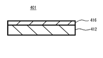
- FIG. 9 is a cross-sectional view of an electric element provided with an oxide thin film.
- an electric element 401 is formed by providing an oxide thin film 416 doped with an element on a base material 412.
- the material of the base material 412 is not particularly limited and can be appropriately selected depending on the intended use.
- a Cu alloy such as Cu or brass can be generally used as a connector terminal.
- Al, Fe or alloys thereof can also be used.
- the thickness of the base material 412 can be appropriately determined according to the application, and the shape of the base material can be a rectangular shape, a cylindrical shape, or other irregular shapes.
- the male terminal 432 and the female terminal 434 are formed using the base material 412.
- the material of the oxide constituting the oxide thin film 416 examples include SnO, SnO 2 , NiO, Ni 2 O 3 , ZnO, CuO 2 , CuAlO 2 , In 2 O 3 , or a mixture thereof. From the viewpoint of inter alia improving the effect of the present invention, the oxide is preferably a SnO and / or SnO 2.
- the element that is doped in the oxide thin film 416 is preferably an element that contributes to the development of conductivity, and includes, for example, at least one selected from the group consisting of F, In, Ga, Tl, As, Sb, and Bi.
- F is preferable
- the oxide thin film 416 is particularly preferably formed of fluorine-doped tin oxide (FTO).
- the thickness of the oxide thin film 416 is, for example, 10 nm to 1 ⁇ m.
- a Ni plating layer may be provided on the base material 412 as needed in order to prevent, for example, Cu or Cu alloy contained in the base material 412 from diffusing on the oxide thin film 416.
- Ni alloy such as Fe—Ni alloy and Sn—Ni alloy can be used in addition to Ni.
- the thickness of the Ni plating layer is determined as appropriate as long as the object can be achieved.
- the base material 412 is prepared, and the surface is polished as necessary. Polishing is performed by a known method for smoothing the surface, such as mechanical polishing or chemical polishing.
- the concave portion 438 is formed in a hemispherical shape, but may have other shapes such as a polygonal shape.
- an oxide thin film 416 doped with an element is provided on the surface of the substrate 412.
- the oxide thin film 416 can be provided by, for example, a spray pyrolysis (SPD: Spray Pyrolysis Deposition) method.
- SPD Spray Pyrolysis Deposition
- the substrate is heated to the film formation temperature and sprayed with the solution that is the raw material of the film using a spraying means such as an atomizer toward the initial stage.
- a spraying means such as an atomizer toward the initial stage.
- Forms a crystal by evaporating the solvent in the droplets attached to the substrate surface, followed by the hydrolysis and thermal oxidation reactions following the thermal decomposition of the solute, and as the reaction proceeds, the droplets form on the crystals.
- the oxide thin film 416 can be pinpointed and / or formed in an arbitrary shape. Note that the oxide thin film 416 can be formed by a known method other than the SPD method.
- the oxide thin film 416 formed in this manner has conductivity (for example, a specific resistance value of 1 ⁇ 10 7 ⁇ ⁇ cm or less), exhibits the effects of the present invention, and wear resistance. Excellent in corrosion resistance, corrosion resistance, heat resistance, etc.
- FIG. 10 is a schematic diagram of a terminal according to the present embodiment.
- a case where an FTO thin film 436 is used as the oxide thin film 416 will be described as an example.
- the male terminal 432 is inserted into the female terminal 434, and the male terminal 432 and the female terminal 434 are conductively connected.
- the in FIG. 10 a male terminal 432 and a female terminal 434 are each made of the base material 412 described above.
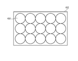
- FIG. 11 is a plan view of the contact portion of the terminal according to the present embodiment.
- the base material 412 of the male terminal 432 for example, a Cu alloy made of brass is used.
- the material of the base material of the male terminal 432 and the female terminal 434 may be different from each other.
- a plurality of concave portions 438 are formed in the contact portion that contacts the female terminal 434 constituting the counterpart terminal, and the openings of these concave portions 438 are formed on the surface of the contact portion. Are arranged so as to contact each other.
- the contact portion means a range where at least the female terminal 434 is in sliding contact with the male terminal 432.
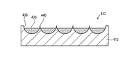
- FIG. 12 is a cross-sectional view of the contact portion of the male terminal 432.
- An FTO thin film 436 is formed in the recess 438 of the male terminal 432 from the bottom of the recess 438 to a predetermined depth.
- the top surface of the FTO thin film 436 is set at a position lower than the surface of the male terminal 432, so that the tops 440 formed by the base material 412 are exposed on the surface of the male terminal 432. is doing.
- the contact portion of the female terminal 434 comes into sliding contact with the FTO thin film 436 and the top portion 440.
- the FTO thin film 436 is formed, the wear resistance of the surface of the male terminal 432 can be improved.
- the male terminal 432 and the female terminal 434 can be conductively connected through both the FTO thin film 436 and the top part 440.
- the diameter of the opening of the recess 438 and the thickness of the FTO thin film 436 are such that the male connector provided with the male terminal 432 is fitted to the female connector provided with the female terminal 434, and the surface of the female terminal 434 is the male terminal 432.
- the opening of the recess 438 and the FTO thin film 436 are preferably set so as to be able to come into contact with each other, but the upper surface of the FTO thin film 436 and the surface of the male terminal 432 are substantially coincident with each other.
- An FTO thin film 436 may be provided.
- the concave portion 438 is formed in the contact portion of the male terminal 432.
- the present invention is not limited to this, and the concave portion 438 may be formed in the contact portion of the female terminal 434. Further, the recess 438 may be formed in both the male terminal 432 and the female terminal 434.
- the male terminal 432 of this embodiment can reduce the cost because it is not necessary to perform noble metal plating on the surface of the base material 412, and the counterpart terminal, the FTO thin film 436 and the top portion 440 can be reduced. Therefore, the wear resistance of the contact portion can be improved.
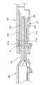
- FIG. 13 is a longitudinal sectional view of a terminal fitting according to a fifth embodiment of the present invention
- FIG. 14 is an enlarged view of a portion A in FIG.
- FIG. 13 the fitting state of the female terminal fitting 510 and the male terminal fitting 520 is shown.
- the female terminal fitting 510 is formed in a predetermined structure by press molding of a metal plate, and a male terminal is provided inside a rectangular tube-like fitting tube portion 511 into which a mating terminal fitting (male terminal fitting 520) is fitted.
- Spring plate portions 512 and 513 for sandwiching the tongue-like piece 521 of the metal fitting 520 are provided.
- Each of the spring plate portions 512 and 513 is formed with projections 512a and 513a with which the tongue-like piece 521 inserted into the fitting tube portion 511 comes into sliding contact.
- These protrusions 512a and 513a are formed in curved surfaces with smooth surfaces.
- the male terminal fitting 520 is formed in a predetermined structure by press-molding a metal plate, and is provided with a tongue-like piece 521 fitted to the fitting cylinder portion 511 of the female terminal fitting 510 at the tip.
- the tongue-like piece 521 has a predetermined thickness dimension by sandwiching both surfaces of a flat cored bar 522 with surface plates 523 and 524.
- the metal plate forming the female terminal fitting 510 and the male terminal fitting 520 described above is a plating material 530 having a multilayer structure shown in FIG. That is, the female terminal fitting 510 and the male terminal fitting 520 are formed by press molding the plating material 530.
- the plating material 530 includes a base metal plate 531, a first plating layer 532 made of silver covering the surface of the base metal plate 531, and a fluorine-doped tin oxide film (FTO) covering the surface of the first plating layer 532. ) And a second plating layer 534 made of tin or a tin alloy covering the fluorine-doped tin oxide film 533, and a plate material having a four-layer structure.
- FTO fluorine-doped tin oxide film
- the substrate is heated to the film formation temperature and sprayed with the solution that is the raw material of the film using a spraying means such as an atomizer toward the initial stage.
- a spraying means such as an atomizer toward the initial stage.
- Forms a crystal by evaporating the solvent in the droplets attached to the substrate surface, followed by the hydrolysis and thermal oxidation reactions following the thermal decomposition of the solute, and as the reaction proceeds, the droplets form on the crystals.
- the fluorine-doped tin oxide can be formed by employing a known method other than the SPD method.
- Fluorine-doped tin oxide has a lower material cost than gold or silver.
- the fluorine-doped tin oxide film has a volume resistivity that is only an order of magnitude higher than that of pure metal of tin (Sn) and has excellent conductivity that is not inferior to gold or silver.
- FTO film fluorine-doped tin oxide film
- Sn pure metal of tin
- have fluorine-doped tin oxide has low conductivity temperature dependency, excellent corrosion resistance and wear resistance, and exhibits excellent durability.
- the base metal plate 531 is, for example, a plate material having a predetermined thickness made of copper (Cu). Further, the first plating layer 532 may be strike plating.
- the plating material 530 is used so that the second plating layer 534 of the plating material 530 serves as a sliding surface between the terminal fittings.
- the fluorine-doped tin oxide film 533 covering the first plating layer 532 made of silver has the following characteristics (a) to (d).
- the second plating layer 534 made of tin or a tin alloy covering the fluorine-doped tin oxide film 533 is more easily deformed than the fluorine-doped tin oxide film 533, and is used in a contact portion with a counterpart member.
- the contact with the mating member can be improved by adapting to the unevenness of the surface of the mating member, and the contact reliability can be improved when used for a terminal fitting or the like.
- the plating material 530 can maintain excellent wear resistance, conductivity, and slidability over a long period of time, and can reduce the cost by suppressing the thickness of the first plating layer 532 made of silver. Can be achieved.
- the sliding surface which is a contact portion between the terminal fittings, is formed on the fluorine-doped tin oxide film 533 with the second plating layer 534 using tin or a tin alloy.
- the slidability and contact reliability with the mating terminal fitting can be improved.
- excellent conductivity can be ensured by the excellent conductivity of the fluorine-doped tin oxide film 533 and the first plating layer 532.
- the fluorine-doped tin oxide film 533 has excellent wear resistance, it is possible to suppress wear and obtain stable connection performance even when the fitting / removal with the mating terminal fitting is repeated.
- the plating material 530 is provided with unevenness 530 a on the surface of the base metal plate 531.
- the first plating layer 532, the fluorine-doped tin oxide film 533, and the second plating layer 534 laminated on the base metal plate 531 are also structured to have the same unevenness as the unevenness 530a of the base metal plate 531. good.
- each layer with respect to the base metal plate 531 can be improved, and even if press molding or the like is performed, the layer is hardly peeled off and each layer can exhibit stable performance.
- the use of the plating material 530 is not limited to the terminal fittings 510 and 520 shown in the above embodiment, but can also be used for a contact pattern provided on a printed circuit board, a slider that slides on the contact, or the like. is there.
- the electric element (1) according to the above [2], wherein the element contributing to conductivity is at least one selected from the group consisting of F, In, Ga, Tl, As, Sb and Bi.
- the electric element (1) according to the above [2], wherein the element contributing to the development of conductivity is F.
- the first conductor layer (203) includes a base conductor layer (231) formed of copper or a copper alloy, and the second conductor layer formed on the base conductor layer (231).
- the plate-like conductor (202) according to the above [9], comprising a base conductor layer (232) made of nickel or a nickel alloy that facilitates the film formation of (204).
- a surface treatment method for a plate-like conductor in which a third conductor layer (205) is formed on the first conductor layer (203) and the second conductor layer (204) with fluorine-doped tin oxide.
- An electrical element male terminal 332) electrically connected to the counterpart terminal (female terminal 334) by being inserted into and contacted with the counterpart terminal (female terminal 334),
- an oxide thin film doped with an element is provided at least in a region in contact with the counterpart terminal (female terminal 334),
- the oxide thin film is provided on the base material (312) in a state where the surface of the base material (312) is smooth,
- the electric element according to [12], wherein the element contributing to the development of conductivity is at least one selected from the group consisting of F, In, Ga, Tl, As, Sb, and Bi.
- a connector comprising the terminal (male terminal 332) according to [15].
- a plating material (530) comprising a tin film (533) and a second plating layer (534) made of tin or a tin alloy covering the fluorine-doped tin oxide film (533).
- the surface of the base metal plate (531) improves adhesion of the first plating layer (532), the fluorine-doped tin oxide film (533), and the second plating layer (534) to the surface.
- the plating material (530) according to the above [21], wherein the unevenness (530a) is provided.
- the present invention it is low-cost and prevents deterioration of product reliability due to oxidation of the base material, and can maintain a large true contact surface even with a small and low contact load electric contact. And the effect of increasing the contact resistance can be solved.
- the present invention that exhibits this effect is useful for electrical elements.
Landscapes
- Chemical & Material Sciences (AREA)
- Organic Chemistry (AREA)
- Engineering & Computer Science (AREA)
- Chemical Kinetics & Catalysis (AREA)
- Materials Engineering (AREA)
- Metallurgy (AREA)
- Electrochemistry (AREA)
- Mechanical Engineering (AREA)
- Inorganic Chemistry (AREA)
- Physics & Mathematics (AREA)
- Thermal Sciences (AREA)
- General Chemical & Material Sciences (AREA)
- Contacts (AREA)
- Electroplating Methods And Accessories (AREA)
Abstract
La présente invention concerne un contact électrique pour connecteurs, un film mince d'oxyde (16) dopé avec un élément étant disposé sur une base (12), ledit élément contribuant au développement de la conductivité électrique. Il est préférable que l'élément contribuant au développement de la conductivité électrique soit au moins un élément choisi dans le groupe constitué par F, In, Ga, Ti, As, Sb et Bi. Il est également préférable que le film mince d'oxyde soit formé de SnO et/ou de SnO2.
Applications Claiming Priority (10)
| Application Number | Priority Date | Filing Date | Title |
|---|---|---|---|
| JP2014144249A JP6374718B2 (ja) | 2014-07-14 | 2014-07-14 | 電気素子 |
| JP2014-144249 | 2014-07-14 | ||
| JP2014145112A JP6268055B2 (ja) | 2014-07-15 | 2014-07-15 | 端子及びコネクタ |
| JP2014-145112 | 2014-07-15 | ||
| JP2014-187830 | 2014-09-16 | ||
| JP2014187830A JP6268070B2 (ja) | 2014-09-16 | 2014-09-16 | メッキ材及び端子金具 |
| JP2014217382A JP6272744B2 (ja) | 2014-10-24 | 2014-10-24 | 板状導電体及び板状導電体の表面処理方法 |
| JP2014-217382 | 2014-10-24 | ||
| JP2014-253432 | 2014-12-15 | ||
| JP2014253432A JP2016113666A (ja) | 2014-12-15 | 2014-12-15 | 電気素子及びコネクタ |
Publications (1)
| Publication Number | Publication Date |
|---|---|
| WO2016010053A1 true WO2016010053A1 (fr) | 2016-01-21 |
Family
ID=55078543
Family Applications (1)
| Application Number | Title | Priority Date | Filing Date |
|---|---|---|---|
| PCT/JP2015/070205 Ceased WO2016010053A1 (fr) | 2014-07-14 | 2015-07-14 | Élément électrique |
Country Status (1)
| Country | Link |
|---|---|
| WO (1) | WO2016010053A1 (fr) |
Cited By (1)
| Publication number | Priority date | Publication date | Assignee | Title |
|---|---|---|---|---|
| CN113491038A (zh) * | 2019-06-05 | 2021-10-08 | 埃尔尼国际股份有限公司 | 电接触元件 |
Citations (7)
| Publication number | Priority date | Publication date | Assignee | Title |
|---|---|---|---|---|
| JP2005048201A (ja) * | 2003-07-29 | 2005-02-24 | Fcm Kk | 端子、それを有する部品および製品 |
| JP2005512302A (ja) * | 2001-12-13 | 2005-04-28 | オウトクンプ オサケイティオ ユルキネン | ドープされたコーティングを有する接触端子 |
| JP2006500759A (ja) * | 2001-10-22 | 2006-01-05 | フリースケール セミコンダクター インコーポレイテッド | 基板への相互接続を有する集積回路およびその製造方法 |
| JP2009084616A (ja) * | 2007-09-28 | 2009-04-23 | Nikko Kinzoku Kk | リフローSnめっき材及びそれを用いた電子部品 |
| JP2012113968A (ja) * | 2010-11-25 | 2012-06-14 | Nippon Electric Glass Co Ltd | 電気素子パッケージ |
| JP2013221166A (ja) * | 2012-04-13 | 2013-10-28 | Jx Nippon Mining & Metals Corp | 電子部品用金属材料 |
| JP2013222659A (ja) * | 2012-04-18 | 2013-10-28 | Auto Network Gijutsu Kenkyusho:Kk | コネクタ用電気接点材料とその製造方法およびコネクタ用電気接点 |
-
2015
- 2015-07-14 WO PCT/JP2015/070205 patent/WO2016010053A1/fr not_active Ceased
Patent Citations (7)
| Publication number | Priority date | Publication date | Assignee | Title |
|---|---|---|---|---|
| JP2006500759A (ja) * | 2001-10-22 | 2006-01-05 | フリースケール セミコンダクター インコーポレイテッド | 基板への相互接続を有する集積回路およびその製造方法 |
| JP2005512302A (ja) * | 2001-12-13 | 2005-04-28 | オウトクンプ オサケイティオ ユルキネン | ドープされたコーティングを有する接触端子 |
| JP2005048201A (ja) * | 2003-07-29 | 2005-02-24 | Fcm Kk | 端子、それを有する部品および製品 |
| JP2009084616A (ja) * | 2007-09-28 | 2009-04-23 | Nikko Kinzoku Kk | リフローSnめっき材及びそれを用いた電子部品 |
| JP2012113968A (ja) * | 2010-11-25 | 2012-06-14 | Nippon Electric Glass Co Ltd | 電気素子パッケージ |
| JP2013221166A (ja) * | 2012-04-13 | 2013-10-28 | Jx Nippon Mining & Metals Corp | 電子部品用金属材料 |
| JP2013222659A (ja) * | 2012-04-18 | 2013-10-28 | Auto Network Gijutsu Kenkyusho:Kk | コネクタ用電気接点材料とその製造方法およびコネクタ用電気接点 |
Cited By (1)
| Publication number | Priority date | Publication date | Assignee | Title |
|---|---|---|---|---|
| CN113491038A (zh) * | 2019-06-05 | 2021-10-08 | 埃尔尼国际股份有限公司 | 电接触元件 |
Similar Documents
| Publication | Publication Date | Title |
|---|---|---|
| JP6183543B2 (ja) | 端子対及び端子対を備えたコネクタ対 | |
| US8018318B2 (en) | Resistive component and method of manufacturing the same | |
| US9004960B2 (en) | Connector with gold-palladium plated contacts | |
| US10177478B2 (en) | Board terminal and board connector | |
| CN104604036A (zh) | 连接器用镀敷端子以及端子对 | |
| WO2012147506A1 (fr) | Matériau de contact électrique pour connecteur, son procédé de production et contact électrique pour connecteur | |
| JP6332043B2 (ja) | コネクタ用端子対 | |
| JP2014201753A (ja) | コネクタ端子材料の製造方法およびコネクタ端子の製造方法 | |
| CN100514759C (zh) | 电连接器用端子、电镀方法和端子连接体 | |
| CN107408772B (zh) | 电气触点对以及连接器用端子对 | |
| JP6374718B2 (ja) | 電気素子 | |
| WO2016010053A1 (fr) | Élément électrique | |
| JP6268055B2 (ja) | 端子及びコネクタ | |
| CN109845041B (zh) | 连接端子及连接端子的制造方法 | |
| US20110086558A1 (en) | Electrical contact with improved material and method manufacturing the same | |
| JP2008182128A (ja) | チップ抵抗器 | |
| JP2016071950A (ja) | 電線及びコネクタ | |
| JP2016113666A (ja) | 電気素子及びコネクタ | |
| JP2015167099A (ja) | コネクタ端子及びその製造方法 | |
| JP6268070B2 (ja) | メッキ材及び端子金具 | |
| CN101673602A (zh) | 电阻元件及其制造方法 | |
| JP6272744B2 (ja) | 板状導電体及び板状導電体の表面処理方法 | |
| JP2016071951A (ja) | 圧着端子 | |
| JP2016115542A (ja) | 電気素子及びコネクタ | |
| JP2025144923A (ja) | 電子部品およびその製造方法 |
Legal Events
| Date | Code | Title | Description |
|---|---|---|---|
| 121 | Ep: the epo has been informed by wipo that ep was designated in this application |
Ref document number: 15821553 Country of ref document: EP Kind code of ref document: A1 |
|
| NENP | Non-entry into the national phase |
Ref country code: DE |
|
| 122 | Ep: pct application non-entry in european phase |
Ref document number: 15821553 Country of ref document: EP Kind code of ref document: A1 |