WO2016017617A1 - Dispositif de conversion photoélectrique, dispositif de conversion photoélectrique en tandem et réseau de dispositifs de conversion photoélectrique - Google Patents
Dispositif de conversion photoélectrique, dispositif de conversion photoélectrique en tandem et réseau de dispositifs de conversion photoélectrique Download PDFInfo
- Publication number
- WO2016017617A1 WO2016017617A1 PCT/JP2015/071326 JP2015071326W WO2016017617A1 WO 2016017617 A1 WO2016017617 A1 WO 2016017617A1 JP 2015071326 W JP2015071326 W JP 2015071326W WO 2016017617 A1 WO2016017617 A1 WO 2016017617A1
- Authority
- WO
- WIPO (PCT)
- Prior art keywords
- photoelectric conversion
- conversion device
- semiconductor layer
- light
- layer
- Prior art date
- Legal status (The legal status is an assumption and is not a legal conclusion. Google has not performed a legal analysis and makes no representation as to the accuracy of the status listed.)
- Ceased
Links
Images



Classifications
-
- H—ELECTRICITY
- H10—SEMICONDUCTOR DEVICES; ELECTRIC SOLID-STATE DEVICES NOT OTHERWISE PROVIDED FOR
- H10F—INORGANIC SEMICONDUCTOR DEVICES SENSITIVE TO INFRARED RADIATION, LIGHT, ELECTROMAGNETIC RADIATION OF SHORTER WAVELENGTH OR CORPUSCULAR RADIATION
- H10F10/00—Individual photovoltaic cells, e.g. solar cells
- H10F10/10—Individual photovoltaic cells, e.g. solar cells having potential barriers
- H10F10/16—Photovoltaic cells having only PN heterojunction potential barriers
- H10F10/161—Photovoltaic cells having only PN heterojunction potential barriers comprising multiple PN heterojunctions, e.g. tandem cells
-
- H—ELECTRICITY
- H10—SEMICONDUCTOR DEVICES; ELECTRIC SOLID-STATE DEVICES NOT OTHERWISE PROVIDED FOR
- H10F—INORGANIC SEMICONDUCTOR DEVICES SENSITIVE TO INFRARED RADIATION, LIGHT, ELECTROMAGNETIC RADIATION OF SHORTER WAVELENGTH OR CORPUSCULAR RADIATION
- H10F10/00—Individual photovoltaic cells, e.g. solar cells
- H10F10/10—Individual photovoltaic cells, e.g. solar cells having potential barriers
- H10F10/16—Photovoltaic cells having only PN heterojunction potential barriers
- H10F10/167—Photovoltaic cells having only PN heterojunction potential barriers comprising Group I-III-VI materials, e.g. CdS/CuInSe2 [CIS] heterojunction photovoltaic cells
-
- H—ELECTRICITY
- H10—SEMICONDUCTOR DEVICES; ELECTRIC SOLID-STATE DEVICES NOT OTHERWISE PROVIDED FOR
- H10F—INORGANIC SEMICONDUCTOR DEVICES SENSITIVE TO INFRARED RADIATION, LIGHT, ELECTROMAGNETIC RADIATION OF SHORTER WAVELENGTH OR CORPUSCULAR RADIATION
- H10F19/00—Integrated devices, or assemblies of multiple devices, comprising at least one photovoltaic cell covered by group H10F10/00, e.g. photovoltaic modules
- H10F19/90—Structures for connecting between photovoltaic cells, e.g. interconnections or insulating spacers
- H10F19/902—Structures for connecting between photovoltaic cells, e.g. interconnections or insulating spacers for series or parallel connection of photovoltaic cells
-
- H—ELECTRICITY
- H10—SEMICONDUCTOR DEVICES; ELECTRIC SOLID-STATE DEVICES NOT OTHERWISE PROVIDED FOR
- H10F—INORGANIC SEMICONDUCTOR DEVICES SENSITIVE TO INFRARED RADIATION, LIGHT, ELECTROMAGNETIC RADIATION OF SHORTER WAVELENGTH OR CORPUSCULAR RADIATION
- H10F77/00—Constructional details of devices covered by this subclass
- H10F77/10—Semiconductor bodies
-
- H—ELECTRICITY
- H10—SEMICONDUCTOR DEVICES; ELECTRIC SOLID-STATE DEVICES NOT OTHERWISE PROVIDED FOR
- H10F—INORGANIC SEMICONDUCTOR DEVICES SENSITIVE TO INFRARED RADIATION, LIGHT, ELECTROMAGNETIC RADIATION OF SHORTER WAVELENGTH OR CORPUSCULAR RADIATION
- H10F77/00—Constructional details of devices covered by this subclass
- H10F77/10—Semiconductor bodies
- H10F77/12—Active materials
- H10F77/126—Active materials comprising only Group I-III-VI chalcopyrite materials, e.g. CuInSe2, CuGaSe2 or CuInGaSe2 [CIGS]
-
- H—ELECTRICITY
- H10—SEMICONDUCTOR DEVICES; ELECTRIC SOLID-STATE DEVICES NOT OTHERWISE PROVIDED FOR
- H10F—INORGANIC SEMICONDUCTOR DEVICES SENSITIVE TO INFRARED RADIATION, LIGHT, ELECTROMAGNETIC RADIATION OF SHORTER WAVELENGTH OR CORPUSCULAR RADIATION
- H10F77/00—Constructional details of devices covered by this subclass
- H10F77/10—Semiconductor bodies
- H10F77/12—Active materials
- H10F77/127—Active materials comprising only Group IV-VI or only Group II-IV-VI chalcogenide materials, e.g. PbSnTe
-
- H—ELECTRICITY
- H10—SEMICONDUCTOR DEVICES; ELECTRIC SOLID-STATE DEVICES NOT OTHERWISE PROVIDED FOR
- H10F—INORGANIC SEMICONDUCTOR DEVICES SENSITIVE TO INFRARED RADIATION, LIGHT, ELECTROMAGNETIC RADIATION OF SHORTER WAVELENGTH OR CORPUSCULAR RADIATION
- H10F77/00—Constructional details of devices covered by this subclass
- H10F77/20—Electrodes
- H10F77/206—Electrodes for devices having potential barriers
- H10F77/211—Electrodes for devices having potential barriers for photovoltaic cells
-
- H—ELECTRICITY
- H10—SEMICONDUCTOR DEVICES; ELECTRIC SOLID-STATE DEVICES NOT OTHERWISE PROVIDED FOR
- H10F—INORGANIC SEMICONDUCTOR DEVICES SENSITIVE TO INFRARED RADIATION, LIGHT, ELECTROMAGNETIC RADIATION OF SHORTER WAVELENGTH OR CORPUSCULAR RADIATION
- H10F77/00—Constructional details of devices covered by this subclass
- H10F77/40—Optical elements or arrangements
- H10F77/42—Optical elements or arrangements directly associated or integrated with photovoltaic cells, e.g. light-reflecting means or light-concentrating means
- H10F77/484—Refractive light-concentrating means, e.g. lenses
-
- Y—GENERAL TAGGING OF NEW TECHNOLOGICAL DEVELOPMENTS; GENERAL TAGGING OF CROSS-SECTIONAL TECHNOLOGIES SPANNING OVER SEVERAL SECTIONS OF THE IPC; TECHNICAL SUBJECTS COVERED BY FORMER USPC CROSS-REFERENCE ART COLLECTIONS [XRACs] AND DIGESTS
- Y02—TECHNOLOGIES OR APPLICATIONS FOR MITIGATION OR ADAPTATION AGAINST CLIMATE CHANGE
- Y02E—REDUCTION OF GREENHOUSE GAS [GHG] EMISSIONS, RELATED TO ENERGY GENERATION, TRANSMISSION OR DISTRIBUTION
- Y02E10/00—Energy generation through renewable energy sources
- Y02E10/50—Photovoltaic [PV] energy
- Y02E10/52—PV systems with concentrators
-
- Y—GENERAL TAGGING OF NEW TECHNOLOGICAL DEVELOPMENTS; GENERAL TAGGING OF CROSS-SECTIONAL TECHNOLOGIES SPANNING OVER SEVERAL SECTIONS OF THE IPC; TECHNICAL SUBJECTS COVERED BY FORMER USPC CROSS-REFERENCE ART COLLECTIONS [XRACs] AND DIGESTS
- Y02—TECHNOLOGIES OR APPLICATIONS FOR MITIGATION OR ADAPTATION AGAINST CLIMATE CHANGE
- Y02E—REDUCTION OF GREENHOUSE GAS [GHG] EMISSIONS, RELATED TO ENERGY GENERATION, TRANSMISSION OR DISTRIBUTION
- Y02E10/00—Energy generation through renewable energy sources
- Y02E10/50—Photovoltaic [PV] energy
- Y02E10/541—CuInSe2 material PV cells
Definitions
- the present invention relates to a photoelectric conversion device using a semiconductor thin film as a photoelectric conversion layer, a tandem photoelectric conversion device using the same, and a photoelectric conversion device array.
- a photoelectric conversion device used for photovoltaic power generation or the like there is a thin film type photoelectric conversion device using a semiconductor thin film having a thickness of about several ⁇ m as a photoelectric conversion layer.
- a material for such a semiconductor layer for example, a chalcopyrite compound such as CIGS, amorphous silicon, or the like is employed (see, for example, JP-A-8-330614).
- Thin-film photoelectric conversion devices are suitable for large area and low cost, and research and development of next-generation solar cells using them are being promoted.
- a lower electrode layer such as a metal electrode, a first semiconductor layer made of a semiconductor thin film, and a second semiconductor layer different from the first semiconductor layer are formed on a substrate such as a glass plate.
- the photoelectric conversion cells stacked in this order are configured by arranging a plurality of planarly arranged photoelectric conversion cells.
- the photoelectric conversion device is always required to improve the photoelectric conversion efficiency.
- As a method of increasing the photoelectric conversion efficiency of the photoelectric conversion device there is a method of increasing the probability of photoelectric conversion by increasing the optical path length in the photoelectric conversion layer of light incident on the photoelectric conversion device. By doing so, it becomes possible to increase the spectral sensitivity to light with a long wavelength, or to further reduce the conversion efficiency by reducing the optical path length, and to form a thin film further. By increasing the photoelectron density, the conversion efficiency can be increased and the cost can be reduced.
- a texture structure consisting of unevenness of about several hundred nm is formed on the surface of the silicon substrate to scatter light on the surface of the silicon substrate.
- the optical path length in the silicon substrate is increased.
- One object of the present invention is to increase the optical path length in a photoelectric conversion layer made of a semiconductor thin film and improve the photoelectric conversion efficiency of the photoelectric conversion device.
- a photoelectric conversion device includes an electrode layer, a first semiconductor layer located on a main surface of the electrode layer, and scattered within the first semiconductor layer or the first semiconductor layer.
- a second semiconductor layer bonded to each other.
- the photoelectric conversion device described above is used as a first photoelectric conversion device, and a photoelectric conversion device having a spectral sensitivity different from that of the first photoelectric conversion device is used as a second photoelectric conversion device.
- a photoelectric conversion device having a spectral sensitivity different from that of the first photoelectric conversion device is used as a second photoelectric conversion device.
- the first photoelectric conversion device and the second photoelectric conversion device are stacked.
- a photoelectric conversion device array In a photoelectric conversion device array according to another aspect of the present invention, a plurality of the tandem photoelectric conversion devices are arranged, and in each of the adjacent tandem photoelectric conversion devices, the first photoelectric conversion devices are connected to each other.
- the second photoelectric conversion devices are electrically connected to each other while being electrically connected to each other.
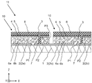
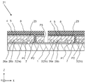
- FIG. 1st Embodiment It is a perspective view which shows the photoelectric conversion apparatus of 1st Embodiment. It is sectional drawing of the photoelectric conversion apparatus shown in FIG. It is sectional drawing of the photoelectric conversion apparatus of 2nd Embodiment. It is a principal part expanded sectional view of the 1st semiconductor layer in the photoelectric conversion apparatus of 3rd Embodiment. It is sectional drawing which shows the tandem photoelectric conversion apparatus and solar cell array of 1st Embodiment.
- FIG. 1 is a perspective view showing a photoelectric conversion device (first embodiment) according to an embodiment of the present invention
- FIG. 2 is an XZ sectional view of the photoelectric conversion device. 1 and 2 have a right-handed XYZ coordinate system in which the arrangement direction of the photoelectric conversion cells 10 (the horizontal direction in the drawing of FIG. 1) is the X-axis direction.
- the photoelectric conversion device 11 of the first embodiment a plurality of photoelectric conversion cells 10 are arranged on a substrate 1 and are electrically connected to each other. In FIG. 1, only two photoelectric conversion cells 10 are shown for the sake of illustration.
- the horizontal direction in the drawing (X-axis direction) or a direction perpendicular thereto is also shown.
- a large number of photoelectric conversion cells 10 may be arranged in a plane (two-dimensionally) in the (Y-axis direction).
- a plurality of lower electrode layers 2 are arranged in a plane on the substrate 1.
- the plurality of lower electrode layers 2 include lower electrode layers 2a to 2c arranged with a spacing P1 in one direction (X-axis direction).
- a first semiconductor layer 3 is provided from the lower electrode layer 2a through the substrate 1 to the lower electrode layer 2b.
- a second semiconductor layer 4 having a conductivity type different from that of the first semiconductor layer 3 is provided on the first semiconductor layer 3.
- the connection conductor 7 is provided along the side surface of the first semiconductor layer 3 or penetrating the first semiconductor layer 3. The connection conductor 7 electrically connects the second semiconductor layer 4 and the lower electrode layer 2b.
- the lower electrode layer 2, the first semiconductor layer 3 and the second semiconductor layer 4 constitute one photoelectric conversion cell 10, and the adjacent photoelectric conversion cells 10 with the gap P3 interposed therebetween through the connection conductor 7. By being connected in series, the high-power photoelectric conversion device 11 is obtained.
- the photoelectric conversion apparatus 11 in this embodiment assumes what enters light from the 2nd semiconductor layer 4 side, it is not limited to this, Light enters from the board
- the substrate 1 is for supporting the photoelectric conversion cell 10.
- Examples of the material used for the substrate 1 include glass, ceramics, resin, and metal.
- the lower electrode layer 2 (lower electrode layers 2a, 2b, 2c) is a layer made of a conductor such as Mo, Al, Ti, or Au provided on the substrate 1.
- the lower electrode layer 2 is formed to a thickness of about 0.2 to 1 ⁇ m using a known thin film forming method such as sputtering or vapor deposition.
- the first semiconductor layer 3 is a photoelectric conversion layer that absorbs light and performs photoelectric conversion.
- the first semiconductor layer 3 is made of a semiconductor thin film.
- the semiconductor thin film is a thin layer made of a semiconductor and having a thickness of 5 ⁇ m or less. From the viewpoint of taking out more positive and negative carriers generated by photoelectric conversion and increasing the photoelectric conversion efficiency, the thickness of the first semiconductor layer 3 may be 1 to 3 ⁇ m.
- the first semiconductor layer 3 is a p-type semiconductor. However, the first semiconductor layer 3 may be an n-type semiconductor.
- the first semiconductor layer 3 a compound semiconductor, a silicon-based semiconductor, or the like can be used.
- the first semiconductor layer 3 may be mainly composed of metal chalcogenide.
- a metal chalcogenide is a compound of a metal element and a chalcogen element.
- the chalcogen element refers to sulfur (S), selenium (Se), and tellurium (Te) among group 16 elements (also referred to as group VI-B elements). That the first semiconductor layer 3 is mainly made of metal chalcogenide means that it contains 70 mol% or more of metal chalcogenide.
- Such metal chalcogenides include chalcopyrite compounds such as I-III-VI group compounds and II-IV-V group compounds. In addition to these, there are I-II-IV-VI group compounds and II-VI group compounds.
- the group I-III-VI compound is a compound of a group 11 element (also referred to as a group IB element), a group 13 element (also referred to as a group III-B element), and a group 16 element.
- I-III-VI group compounds include CuInSe 2 (also referred to as copper indium selenide, also referred to as CIS), Cu (In, Ga) Se 2 (also referred to as copper indium diselenide / gallium, also referred to as CIGS), Cu (In , Ga) (Se, S) 2 (diselen / copper indium / gallium, also referred to as CIGSS).
- the 1st semiconductor layer 3 may be the structure from which a composition differs in the thickness direction like CIGS which has a CIGSS layer as a surface layer. From the viewpoint of obtaining higher photoelectric conversion efficiency, an I-III-VI group compound may be used as the first semiconductor layer 3.
- II-IV-V group compounds are group 12 elements (also referred to as II-B group elements), group 14 elements (also referred to as group IV-B elements), and group 15 elements (also referred to as group VB elements).
- the II-IV-V group compound include CdSnP 2 , CdGeAs 2 , CdGeP 2 , CdSiAs 2 , CdSiP 2 , ZnSnSb 2 , ZnSnAs 2 , ZnSnP 2 , ZnGeAs 2 , ZnGeP 2 , and ZnSiAs 2 .
- the I-II-IV-VI group compound is a compound semiconductor of a group 11 element, a group 12 element, a group 14 element and a group 16 element.
- Examples of the I-II-IV-VI group compound include Cu 2 ZnSnS 4 (also referred to as CZTS) and Cu 2 ZnSnS 4-x Se x (also referred to as CZTSSe, where x is a number greater than 0 and less than 4. ), Cu 2 ZnSnSe 4 (also referred to as CZTSe), and the like.
- II-VI group compounds are compound semiconductors of group 12 elements and group 16 elements. Examples of II-VI group compounds include CdTe.
- the first semiconductor layer 3 is mainly made of an organic-inorganic composite material.
- the organic-inorganic composite material is a material in which an organic component and an inorganic component are combined at a molecular level, and examples thereof include CH 3 NH 3 PbX 3 (X is a halogen element) having a perovskite crystal structure.
- the bodies 6a and 6b are scattered.
- the light scatterers 6 a are scattered inside the first semiconductor layer 3, and the light scatterers 6 b are scattered at the interface between the first semiconductor layer 3 and the lower electrode layer 2. is doing.
- the first semiconductor layer 3 does not have to have both the light scatterer 6a located inside and the light scatterer 6b located at the interface with the lower electrode layer 2, but the light scatterer located inside. You may have only the body 6a, or you may have only the light-scattering body 6b located in the interface with the lower electrode layer 2.
- the light incident on the first semiconductor layer 3 can be scattered by the light scatterers 6a and 6b, and the optical path length in the first semiconductor layer 3 can be reduced. Can be long. Thereby, in particular, the spectral sensitivity to light having a long wavelength can be increased. As a result, the probability of photoelectric conversion increases and the photoelectric conversion efficiency can be increased.
- the light transmission type photoelectric conversion device 11 can be formed. Even in this case, the effect of light scattering inside the first semiconductor layer 3 and the apparent effect as compared with the conventional light transmission type photoelectric conversion device in which the light transmittance is improved by thinning the semiconductor layer.
- the photoelectric conversion efficiency is increased by the effect that the generation of a leak source such as pinholes due to the thinning is reduced because the film is thick.
- the distribution of the light scatterers 6a and 6b when the first semiconductor layer 3 is seen through on a plane may be made different depending on the part, so that a desired pattern shape, for example, a character, a figure, or a pattern may be obtained. In this way, a desired pattern can be drawn on the photoelectric conversion device 11 without using paint or the like. In other words, the light reflected by the photoelectric conversion device 11 or the light transmitted through the photoelectric conversion device 11 can be shaded or have a different color tone depending on the distribution of the light scatterers 6a and 6b.
- the contents of the light scatterers 6a and 6b may be made different for each part.
- a pattern can be formed by using a coating method when forming the first semiconductor layer 3, preparing raw material liquids having different contents of the light scatterers 6a, and coating them separately.
- a coating method generally used for drawing such as screen printing or spray coating, is also effective.
- the light scatterers 6 a are scattered inside the first semiconductor layer 3, and the light scatterers 6 b are also formed at the interface between the first semiconductor layer 3 and the lower electrode layer 2.
- the photoelectric conversion efficiency is further improved.
- the light incident on the first semiconductor layer 3 can be favorably scattered by both the light scatterers 6a and 6b, and the first semiconductor layer 3 and the lower electrode layer 2 can be scattered by the light scatterer 6b. It is possible to reduce defects that are likely to be generated at the interface of the metal and suppress carrier recombination.
- the plurality of insulating light scatterers 6a and 6b are scattered in at least one of the inside of the first semiconductor layer 3 and the surface on the lower electrode layer 2 side.
- a plurality of light scatterers 6a and 6b are present at intervals.
- the light scatterers 6a and 6b may be aggregates in which a plurality of aggregates are present, and the aggregates only need to exist at intervals.
- the occupied area ratio of the light scatterers 6a and 6b may be about 2 to 30%.
- the size of each light scatterer 6a, 6b may be about 50 to 600 nm. That is, if the size of the light scatterers 6a and 6b is 50 nm or more, light can be more effectively dispersed. Further, if the size of the light scatterers 6a and 6b is 600 nm or less, the stress due to the difference in thermal expansion between the light scatterers 6a and 6b and the first semiconductor layer 3 can be effectively reduced, and the first semiconductor Generation of cracks in the layer 3 can be reduced.
- the size of the light scatterers 6a and 6b refers to the distance between any two points on the outer periphery of each of the light scatterers 6a and 6b when the XY cross section of the portion where the light scatterers 6a and 6b are present is observed. Is the average value of a plurality of (for example, 10 or more) light scatterers 6a and 6b.
- the electrical resistivity of the light scatterers 6a and 6b may be such that the volume resistivity is 10 10 ⁇ cm or more, preferably 10 12 ⁇ cm or more. .
- the absolute value of the difference between the refractive index of the light scatterers 6a and 6b and the refractive index of the first semiconductor layer 3 is 0.8 or more. There may be.
- refractive indexes for example, CIGS (refractive index is around 3), CH 3 NH 3 PbI 3 having a perovskite crystal structure, etc. (refractive index is around 2.6) are used as the first semiconductor layer 3.
- CIGS refractive index is around 3
- CH 3 NH 3 PbI 3 having a perovskite crystal structure, etc. refractive index is around 2.6
- the light scatterers 6a and 6b a combination using aluminum oxide (refractive index is about 1.7) or silicon oxide (refractive index is about 1.5) can be used.
- the light scatterers 6a and 6b may have a light reflectance of 60% or more, preferably 80% or more in the light wavelength region absorbed by the first semiconductor layer 3. Thereby, the light used for photoelectric conversion can be scattered more favorably.
- white insulating inorganic particles can be used as such light scatterers 6a and 6b. Specific examples of the white insulating inorganic particles include aluminum oxide and silicon oxide. If the light scatterers 6a and 6b are aluminum oxide or silicon oxide, the selectivity of wettability with the first semiconductor layer 3 is widened.
- the shape of the light scatterers 6a and 6b is not particularly limited, but for example, if it is spherical, it can be easily contained in the first semiconductor layer 3.
- the surfaces of the light scatterers 6a and 6b may have irregularities. With such a configuration, the light scattering effect of the light scatterers 6a and 6b can be further increased, and the optical path length of the light incident on the first semiconductor layer 3 can be increased to increase the probability of photoelectric conversion. Can do.
- the surface of the light scatterers 6a and 6b has irregularities means that the outer periphery is not a gently curved surface but has a plurality of irregularities when the cross section of the light scatterers 6a and 6b is observed.
- the light scatterers 6a and 6b having irregularities on the surface may be a combined body (may be an aggregate) by combining a plurality of fine particles, or may be a crushed particle.
- the light scatterers 6a and 6b may be porous bodies having pores with an average pore diameter of about 0.1 to 1 nm. With such a configuration, the light scattering effect can be further enhanced and the adhesiveness with the first semiconductor layer 3 is improved.
- An example of such a porous body is zeolite.
- the average pore diameter can be measured by measuring the cross section of the light scatterers 6a and 6b by the X-ray small angle scattering method.
- Such porous light scatterers 6a and 6b include those in which a plurality of fine particles are bonded together so that a gap is formed therein to form a combined body (or an aggregate).
- the second semiconductor layer 4 is a semiconductor layer having an n-type conductivity different from that of the first semiconductor layer 3.
- a photoelectric conversion layer from which charges can be favorably extracted is formed.
- the second semiconductor layer 4 may be composed of a plurality of layers, and at least one of the plurality of layers may be a high resistance layer.
- the second semiconductor layer 4 includes CdS, ZnS, ZnO, In 2 S 3 , In 2 Se 3 , In (OH, S), (Zn, In) (Se, OH), and (Zn, Mg) O. Etc.
- the second semiconductor layer 4 is formed with a thickness of 10 to 200 nm by, for example, a chemical bath deposition (CBD) method or the like.
- CBD chemical bath deposition
- In (OH, S) refers to a mixed crystal compound containing In as a hydroxide and a sulfide.
- Zn, In) (Se, OH) refers to a mixed crystal compound containing Zn and In as selenides and hydroxides.
- (Zn, Mg) O refers to a compound containing Zn and Mg as oxides.
- an upper electrode layer 5 may be further provided on the second semiconductor layer 4.
- the upper electrode layer 5 is a layer having a lower resistivity than the second semiconductor layer 4.
- the resistivity of the upper electrode layer 5 may be less than 1 ⁇ ⁇ cm and the sheet resistance may be 50 ⁇ / ⁇ or less.
- the upper electrode layer 5 is a transparent conductive film made of, for example, ITO or ZnO and having a thickness of 0.05 to 3 ⁇ m.
- the upper electrode layer 5 may be formed of a semiconductor having the same conductivity type as the second semiconductor layer 4.
- the upper electrode layer 5 can be formed by sputtering, vapor deposition, chemical vapor deposition (CVD), or the like.
- a collecting electrode 8 may be further formed on the upper electrode layer 5.
- the current collecting electrode 8 is for taking out charges generated in the first semiconductor layer 3 and the second semiconductor layer 4 more satisfactorily.
- the collector electrode 8 is formed in a linear shape from one end of the photoelectric conversion cell 10 to the connection conductor 7.
- the electric charges generated in the first semiconductor layer 3 and the second semiconductor layer 4 are collected by the current collecting electrode 8 through the upper electrode layer 5, and are supplied to the adjacent photoelectric conversion cell 10 through the connection conductor 7. It is energized well.
- the collecting electrode 8 may have a width of 50 to 400 ⁇ m from the viewpoint of increasing the light transmittance to the first semiconductor layer 3 and having good conductivity.
- the current collecting electrode 8 may have a plurality of branched portions.
- the current collecting electrode 8 is formed, for example, by printing a metal paste in which a metal powder such as Ag is dispersed in a resin binder or the like in a pattern and curing it.
- connection conductor 7 is a conductor provided in the groove P2 that divides the first semiconductor layer 3, the second semiconductor layer 4, and the upper electrode layer 5.
- connection conductor 7 metal, conductive paste, or the like can be used.
- the current collecting electrode 8 is extended to form the connection conductor 7, but the present invention is not limited to this.
- the upper electrode layer 5 may be stretched.
- the photoelectric conversion device 11 having the above configuration.
- the first semiconductor layer 3 is a metal chalcogenide
- the lower electrode layer 2 made of Mo or the like is formed in a desired pattern on the main surface of the substrate 1 made of glass or the like using a sputtering method or the like.
- the first semiconductor layer 3 including the light scatterers 6 a and 6 b is formed on the main surface of the lower electrode layer 2.
- the following may be performed.
- the first semiconductor layer 3 is formed on the main surface of the lower electrode layer 2 to which the light scatterer 6b is deposited.
- a coating method using a raw material liquid in which a metal complex or a metal salt that is a raw material of the first semiconductor layer 3 is dispersed or dissolved in an organic solvent may be employed. it can.
- the raw material liquid is applied onto the main surface of the lower electrode layer 2 to form a film containing a metal element, and then the film is heated to 450 to 650 ° C. in an atmosphere containing a chalcogen element. Thereby, this film can be formed into the first semiconductor layer 3 mainly containing metal chalcogenide.
- the first semiconductor layer 3 is obtained by adding the light scatterer 6a to the raw material liquid.
- the semiconductor layer 3 may be formed.
- the first semiconductor layer 3 may be formed as a stacked body of a plurality of semiconductor layers as described below, and the light scatterer 6a may be provided at the interface between these semiconductor layers.
- the dispersion liquid is applied onto the semiconductor layer, and the light scatterer 6a is deposited on the semiconductor layer.
- a second semiconductor layer may be formed on the semiconductor layer to which the light scatterer 6a is deposited using the raw material liquid.
- the raw material liquid for example, when the first semiconductor layer 3 is CIGS, a single source complex in which Cu, In, and Se are contained in one organic complex compound, or Cu, Ga, and Se are included.
- a single source complex contained in one organic complex compound (see US Pat. No. 6,992,202) dissolved in a solvent such as pyridine or aniline can be used.
- the second semiconductor layer 4 and the upper electrode layer 5 are formed on the main surface of the first semiconductor layer 3 opposite to the lower electrode layer 2 by the CBD method or the sputtering method. And so on. Then, the first semiconductor layer 3, the second semiconductor layer 4, and the upper electrode layer 5 are processed by mechanical scribing or the like to form a groove for the connection conductor 7.
- the first semiconductor layer 3 to the collector electrode 8 are removed by mechanical scribing at a position shifted from the connection conductor 7 and divided into a plurality of photoelectric conversion cells 10, as shown in FIGS. 1 and 2.
- the photoelectric conversion device 11 can be obtained.
- the light scatterer 6a of the present embodiment even if a hole block layer, an electron block layer, a p-type layer, an n-type layer, or the like is further added to the first semiconductor layer 3, the light scatterer 6a of the present embodiment, The effect by addition of 6b can be acquired.
- the first semiconductor layer 3 is an organic-inorganic composite material such as CH 3 NH 3 PbX 3 (X is a halogen element) having a perovskite crystal structure
- X is a halogen element
- a solution in which an organic-inorganic composite material is dissolved in an organic solvent such as dimethylformamide (DMF) may be used.
- the photoelectric conversion device 11 can be manufactured in the same manner as the manufacturing method of the photoelectric conversion device 11 described above in other steps.
- the photoelectric conversion device 11 of the first embodiment may further include any one or more of a hole block layer, an electron block layer, and a hole transport layer in addition to the above-described configuration.
- the photoelectric conversion device of the second embodiment or the third embodiment described below may be used.
- FIG. 3 is a cross-sectional view of a photoelectric conversion device (second embodiment) according to another embodiment of the present invention.
- the first semiconductor layer 23 has a light scatterer 26a inside, and the content of the light scatterer 26a in the first semiconductor layer 23 is the first.
- the photoelectric conversion device 11 according to the first embodiment is smaller in the portion from the center in the thickness direction to the second semiconductor layer 4 side than the portion from the center in the thickness direction of the semiconductor layer 3 to the lower electrode layer 2 side. Is different.
- parts having the same configurations as those in FIGS. 1 and 2 are denoted by the same reference numerals.
- the volume of the lower electrode layer 2 side of the 1st semiconductor layer 23 side is enlarged, enlarging the volume of the site
- the light path length can be increased by efficiently performing light scattering at the site. As a result, the photoelectric conversion efficiency can be further increased.
- the photoelectric conversion device 21 of the second embodiment may include a light scatterer 26b at the interface between the first semiconductor layer 23 and the lower electrode layer 2, as shown in FIG. This further increases the photoelectric conversion efficiency.
- FIG. 4 is an enlarged cross-sectional view of the main part of the first semiconductor layer 13 in the photoelectric conversion device (third embodiment) according to another embodiment of the present invention.
- the photoelectric conversion device of the third embodiment is different from the photoelectric conversion device 11 of the first embodiment in that the first semiconductor layer 13 has a hole 13a inside.
- the light is easily scattered not only by the light scatterer 16a but also by the holes 13a, and the optical path length of the incident light in the first semiconductor layer 13 is further increased, so that the photoelectric conversion can be performed. Probability can be further increased. Furthermore, even if stress is applied to the first semiconductor layer 13 due to temperature changes during use, the holes 13a effectively relieve the stress and effectively reduce the occurrence of cracks in the first semiconductor layer 13. it can.
- the light scatterer 16a may be positioned on the inner surface of the hole 13a. In this case, even if the first semiconductor layer 13 has the hole 13a by satisfactorily filling the defects of the first semiconductor layer 13 on the inner surface of the hole 13a with the light scatterer 16a, Carrier recombination on the inner surface of the hole 13a can be effectively suppressed.
- the size of the holes 13a may be about 100 to 500 nm.
- the size of the holes 13a refers to an average value obtained by averaging the respective maximum diameters measured for a plurality of (for example, 10 or more) holes 13a when the first semiconductor layer 13 is observed in cross section. .
- the occupied area of the holes 13a in the cross section of the first semiconductor layer 13 that is, the first semiconductor layer 13 including the holes 13a.
- the area occupied by the holes 13a with respect to the area may be about 5 to 50%.
- the size of the holes 13a may be larger than the size of the light scatterers 16a and 16b. With such a configuration, the light scattering angle can be further increased and the photoelectric conversion efficiency can be further increased. From the viewpoint of further improving the photoelectric conversion efficiency while effectively relieving the stress of the first semiconductor layer 13, the size of the holes 13a is 2 to 10 times the size of the light scatterers 16a and 16b. Good.
- Such a first semiconductor layer 13 is a raw material obtained by dispersing a raw material and a light scatterer 16a in an organic solvent in the step of forming the first semiconductor layer shown in the method for manufacturing the photoelectric conversion device of the first embodiment.
- the holes 13a can be included in the first semiconductor layer 13 by adjusting the heating conditions, for example, by rapidly heating.
- the photoelectric conversion device of each of the above embodiments is a first photoelectric conversion device 101, and another photoelectric conversion device having a spectral sensitivity different from that of the first photoelectric conversion device 101.
- the second photoelectric conversion device 102 the first photoelectric conversion device 101 and the second photoelectric conversion device 102 may be stacked so that the principal surfaces face each other to form the tandem photoelectric conversion device 100. .
- first photoelectric conversion device 101 and the second photoelectric conversion device 102 may have a parallel tandem structure in which the insulating layer 103 or the gap is provided to extract power separately, or the first photoelectric conversion device A series tandem structure may be employed in which the device 101 and the second photoelectric conversion device 102 are arranged to be electrically connected to each other. Further, the second photoelectric conversion device 102 may be the photoelectric conversion device of each of the above embodiments as long as spectral sensitivity is different from that of the first photoelectric conversion device 101.
- the first photoelectric conversion device 101 may be positioned in front of the incident direction of light (the side on which light is incident first) and rearward (after which light is incident) than the second photoelectric conversion device 102. Side).
- the photoelectric conversion device positioned in front of the light incident direction may be configured to transmit a part of light according to the spectral sensitivity of the photoelectric conversion device positioned rearward.
- a light scatterer that scatters light absorbed by the first photoelectric conversion device 101 is disposed in the first photoelectric conversion device 101.
- the optical path length of the light can be extended to absorb more light that can be absorbed by the first photoelectric conversion device 101, and the photoelectric conversion efficiency can be increased.
- the same effect can be achieved by forming a metal or the like on the back surface and reflecting the light.
- the second photoelectric conversion device can absorb light that is difficult to be absorbed by the first photoelectric conversion device 101. Since it is necessary to make it enter into 102, it is difficult to use the metal which reflects and does not permeate
- a light scatterer may be arranged.
- the second photoelectric conversion device 102 is made of, for example, a single crystal or the like and is a material in which the light scatterer cannot be disposed, the second photoelectric conversion device is used by the second light scatterer.
- the optical path length in 102 can be increased, and the photoelectric conversion efficiency can be increased.
- the second light scatterer the same light scatterer as described above can be used.
- the second light scatterer is provided between the first photoelectric conversion device 101 and the second photoelectric conversion device 102 as being dispersed in an insulating layer 103 made of, for example, a light-transmitting resin.
- the second photoelectric conversion device 102 may be a photoelectric conversion device using polycrystalline silicon, single crystal silicon, or the like. There are various forms such as a back contact type or a double-sided power generation type, but by connecting the first photoelectric conversion device 101 and the second photoelectric conversion device 102 in parallel electrically, current matching is performed. The influence of loss can be reduced and the conversion efficiency can be increased. In this case, since the insulating layer 103 can be formed between the first photoelectric conversion device 101 and the second photoelectric conversion device 102, the above-described second light scatterer can be disposed here. become able to.
- the second photoelectric conversion device 102 may be a photoelectric conversion device using a chalcopyrite compound such as CIGS.
- the band gap is made smaller than that of the first photoelectric conversion device 101.
- the back contact photoelectric conversion device is a photoelectric conversion device having a structure in which both positive and negative electrodes are drawn to the back surface side.
- a double-sided power generation type photoelectric conversion device is a photoelectric conversion device that can generate power by either light incident from the front surface or light incident from the back surface.
- a plurality of such tandem photoelectric conversion devices may be arranged to form a photoelectric conversion device array 200 as shown in FIG.
- the first photoelectric conversion devices 101 are electrically connected to each other via the wiring 104 a, and the second photoelectric conversion device is used.
- 102 are electrically connected to each other through a wiring 104b.
- the amount of power generation can be further increased.
- electric power is taken out from the tandem photoelectric conversion device 100 located at the end via the wiring 105.
- the photoelectric conversion device was evaluated as follows. First, the raw material liquid for producing the 1st semiconductor layer which consists of CIGS was prepared. In the raw material liquid, a single source complex containing Cu, In and Se in one organic complex compound and a single source complex containing Cu, Ga and Se in one organic complex compound are Cu: In: It was dissolved in pyridine so that Ga: Se was 1: 1: 1: 2. Next, this raw material liquid is divided into a plurality of samples, and for each sample, alumina powder having an average particle size of 200 to 500 nm is dispersed as a light scatterer with varying addition amounts as follows. (Sample) was prepared.
- each of the first semiconductor layers exhibits absorption characteristics with respect to the wavelength in the visible light region, and the position of the absorption edge on the long wavelength side is 1020 nm in the sample 1, whereas it is 1060 nm in the sample 2.
- Sample 3 was 1070 nm and Sample 4 was 1100 nm. Therefore, by adding and dispersing the light scatterer in the first semiconductor layer, the optical path length in the first semiconductor layer can be increased and the spectral sensitivity to light having a long wavelength can be increased. all right.
Landscapes
- Photovoltaic Devices (AREA)
- Life Sciences & Earth Sciences (AREA)
- Engineering & Computer Science (AREA)
- Sustainable Energy (AREA)
- Sustainable Development (AREA)
Abstract
Priority Applications (3)
| Application Number | Priority Date | Filing Date | Title |
|---|---|---|---|
| EP15826705.4A EP3176831A4 (fr) | 2014-07-29 | 2015-07-28 | Dispositif de conversion photoélectrique, dispositif de conversion photoélectrique en tandem et réseau de dispositifs de conversion photoélectrique |
| US15/328,861 US20170213933A1 (en) | 2014-07-29 | 2015-07-28 | Photoelectric conversion device, tandem photoelectric conversion device, and photoelectric conversion device array |
| JP2016538354A JPWO2016017617A1 (ja) | 2014-07-29 | 2015-07-28 | 光電変換装置およびタンデム型光電変換装置ならびに光電変換装置アレイ |
Applications Claiming Priority (2)
| Application Number | Priority Date | Filing Date | Title |
|---|---|---|---|
| JP2014153534 | 2014-07-29 | ||
| JP2014-153534 | 2014-07-29 |
Publications (1)
| Publication Number | Publication Date |
|---|---|
| WO2016017617A1 true WO2016017617A1 (fr) | 2016-02-04 |
Family
ID=55217517
Family Applications (1)
| Application Number | Title | Priority Date | Filing Date |
|---|---|---|---|
| PCT/JP2015/071326 Ceased WO2016017617A1 (fr) | 2014-07-29 | 2015-07-28 | Dispositif de conversion photoélectrique, dispositif de conversion photoélectrique en tandem et réseau de dispositifs de conversion photoélectrique |
Country Status (4)
| Country | Link |
|---|---|
| US (1) | US20170213933A1 (fr) |
| EP (1) | EP3176831A4 (fr) |
| JP (1) | JPWO2016017617A1 (fr) |
| WO (1) | WO2016017617A1 (fr) |
Cited By (5)
| Publication number | Priority date | Publication date | Assignee | Title |
|---|---|---|---|---|
| WO2017142064A1 (fr) * | 2016-02-18 | 2017-08-24 | 積水化学工業株式会社 | Module d'éléments de conversion photoélectrique à jonction solide et son procédé de fabrication |
| JP2018056233A (ja) * | 2016-09-27 | 2018-04-05 | 積水化学工業株式会社 | 太陽電池 |
| KR20180130397A (ko) * | 2017-05-29 | 2018-12-07 | 엘지전자 주식회사 | 페로브스카이트 실리콘 텐덤 태양전지의 제조 방법 |
| CN109643764A (zh) * | 2016-08-31 | 2019-04-16 | 京瓷株式会社 | 太阳能电池及太阳能电池的制造方法 |
| JP2021132233A (ja) * | 2016-09-21 | 2021-09-09 | 株式会社東芝 | 太陽電池モジュール及び太陽光発電システム |
Families Citing this family (1)
| Publication number | Priority date | Publication date | Assignee | Title |
|---|---|---|---|---|
| DE102021123652A1 (de) | 2021-09-13 | 2023-03-16 | Meyer Burger (Germany) Gmbh | Tandem-Solarzelle |
Citations (4)
| Publication number | Priority date | Publication date | Assignee | Title |
|---|---|---|---|---|
| JP2010527045A (ja) * | 2007-05-16 | 2010-08-05 | エルジー・ケム・リミテッド | アンチグレアフィルム用組成物およびそれを用いて製造したアンチグレアフィルム |
| JP2011187885A (ja) * | 2010-03-11 | 2011-09-22 | Fujifilm Corp | 光電変換素子及び太陽電池 |
| JP2012015234A (ja) * | 2010-06-30 | 2012-01-19 | Kyocera Corp | 光電変換装置の製造方法 |
| WO2012029250A1 (fr) * | 2010-08-31 | 2012-03-08 | 株式会社カネカ | Dispositif de conversion photoélectrique empilé en parallèle, et dispositif de conversion photoélectrique intégré en série |
Family Cites Families (5)
| Publication number | Priority date | Publication date | Assignee | Title |
|---|---|---|---|---|
| JP4959127B2 (ja) * | 2004-10-29 | 2012-06-20 | 三菱重工業株式会社 | 光電変換装置及び光電変換装置用基板 |
| US20100252103A1 (en) * | 2009-04-03 | 2010-10-07 | Chiu-Lin Yao | Photoelectronic element having a transparent adhesion structure and the manufacturing method thereof |
| CN102893410A (zh) * | 2010-04-27 | 2013-01-23 | 京瓷株式会社 | 光电转换装置 |
| KR101220060B1 (ko) * | 2011-04-08 | 2013-01-21 | 엘지이노텍 주식회사 | 태양전지 및 이의 제조방법 |
| KR101896951B1 (ko) * | 2011-10-13 | 2018-09-12 | 엘지이노텍 주식회사 | 태양전지 및 이의 제조방법 |
-
2015
- 2015-07-28 WO PCT/JP2015/071326 patent/WO2016017617A1/fr not_active Ceased
- 2015-07-28 JP JP2016538354A patent/JPWO2016017617A1/ja active Pending
- 2015-07-28 US US15/328,861 patent/US20170213933A1/en not_active Abandoned
- 2015-07-28 EP EP15826705.4A patent/EP3176831A4/fr not_active Withdrawn
Patent Citations (4)
| Publication number | Priority date | Publication date | Assignee | Title |
|---|---|---|---|---|
| JP2010527045A (ja) * | 2007-05-16 | 2010-08-05 | エルジー・ケム・リミテッド | アンチグレアフィルム用組成物およびそれを用いて製造したアンチグレアフィルム |
| JP2011187885A (ja) * | 2010-03-11 | 2011-09-22 | Fujifilm Corp | 光電変換素子及び太陽電池 |
| JP2012015234A (ja) * | 2010-06-30 | 2012-01-19 | Kyocera Corp | 光電変換装置の製造方法 |
| WO2012029250A1 (fr) * | 2010-08-31 | 2012-03-08 | 株式会社カネカ | Dispositif de conversion photoélectrique empilé en parallèle, et dispositif de conversion photoélectrique intégré en série |
Non-Patent Citations (1)
| Title |
|---|
| See also references of EP3176831A4 * |
Cited By (11)
| Publication number | Priority date | Publication date | Assignee | Title |
|---|---|---|---|---|
| WO2017142064A1 (fr) * | 2016-02-18 | 2017-08-24 | 積水化学工業株式会社 | Module d'éléments de conversion photoélectrique à jonction solide et son procédé de fabrication |
| JPWO2017142064A1 (ja) * | 2016-02-18 | 2018-12-20 | 積水化学工業株式会社 | 固体接合型光電変換素子モジュール、及びその製造方法 |
| CN109643764A (zh) * | 2016-08-31 | 2019-04-16 | 京瓷株式会社 | 太阳能电池及太阳能电池的制造方法 |
| JPWO2018043644A1 (ja) * | 2016-08-31 | 2019-06-24 | 京セラ株式会社 | 太陽電池および太陽電池の製造方法 |
| EP3509118A4 (fr) * | 2016-08-31 | 2020-04-22 | KYOCERA Corporation | Cellule solaire et procédé de fabrication de cellule solaire |
| US11011718B2 (en) | 2016-08-31 | 2021-05-18 | Kyocera Corporation | Solar cell and method for manufacturing solar cell |
| CN109643764B (zh) * | 2016-08-31 | 2023-04-04 | 京瓷株式会社 | 太阳能电池及太阳能电池的制造方法 |
| JP2021132233A (ja) * | 2016-09-21 | 2021-09-09 | 株式会社東芝 | 太陽電池モジュール及び太陽光発電システム |
| JP2018056233A (ja) * | 2016-09-27 | 2018-04-05 | 積水化学工業株式会社 | 太陽電池 |
| KR20180130397A (ko) * | 2017-05-29 | 2018-12-07 | 엘지전자 주식회사 | 페로브스카이트 실리콘 텐덤 태양전지의 제조 방법 |
| KR102457927B1 (ko) * | 2017-05-29 | 2022-10-25 | 상라오 징코 솔라 테크놀러지 디벨롭먼트 컴퍼니, 리미티드 | 페로브스카이트 실리콘 텐덤 태양전지의 제조 방법 |
Also Published As
| Publication number | Publication date |
|---|---|
| JPWO2016017617A1 (ja) | 2017-04-27 |
| EP3176831A1 (fr) | 2017-06-07 |
| US20170213933A1 (en) | 2017-07-27 |
| EP3176831A4 (fr) | 2018-03-07 |
Similar Documents
| Publication | Publication Date | Title |
|---|---|---|
| WO2016017617A1 (fr) | Dispositif de conversion photoélectrique, dispositif de conversion photoélectrique en tandem et réseau de dispositifs de conversion photoélectrique | |
| CN104115283A (zh) | 太阳能电池模块及其制造方法 | |
| JP6258884B2 (ja) | 光電変換装置 | |
| JP2016171186A (ja) | 光電変換装置 | |
| JP5902592B2 (ja) | 光電変換装置の製造方法 | |
| KR101765922B1 (ko) | 태양전지 및 이의 제조방법 | |
| JP6039695B2 (ja) | 光電変換装置 | |
| US20140290741A1 (en) | Photoelectric conversion apparatus | |
| JP6189604B2 (ja) | 光電変換装置 | |
| JP6346058B2 (ja) | 光電変換装置 | |
| KR101792898B1 (ko) | 태양광 발전장치 및 이의 제조방법 | |
| JP2016122743A (ja) | 光電変換装置 | |
| JP2015225970A (ja) | 光電変換装置 | |
| JP2016184652A (ja) | 光電変換装置 | |
| WO2013111495A1 (fr) | Dispositif de conversion photoélectrique | |
| JP2016157806A (ja) | 光電変換装置 | |
| JP2013149650A (ja) | 光電変換装置 | |
| JP2015099836A (ja) | 光電変換装置 | |
| JP2013110341A (ja) | 光電変換装置 | |
| JP2016111310A (ja) | 光電変換装置 | |
| JP2016219627A (ja) | 光電変換装置 | |
| JP2015126005A (ja) | 光電変換装置 | |
| JP2015204305A (ja) | 光電変換装置の製造方法 | |
| JP2015008218A (ja) | 光電変換装置 | |
| JP2013065818A (ja) | 光電変換装置の製造方法 |
Legal Events
| Date | Code | Title | Description |
|---|---|---|---|
| 121 | Ep: the epo has been informed by wipo that ep was designated in this application |
Ref document number: 15826705 Country of ref document: EP Kind code of ref document: A1 |
|
| ENP | Entry into the national phase |
Ref document number: 2016538354 Country of ref document: JP Kind code of ref document: A |
|
| REEP | Request for entry into the european phase |
Ref document number: 2015826705 Country of ref document: EP |
|
| WWE | Wipo information: entry into national phase |
Ref document number: 2015826705 Country of ref document: EP |
|
| WWE | Wipo information: entry into national phase |
Ref document number: 15328861 Country of ref document: US |
|
| NENP | Non-entry into the national phase |
Ref country code: DE |