WO2016031994A1 - 圧電磁器板および板状基体ならびに電子部品 - Google Patents
圧電磁器板および板状基体ならびに電子部品 Download PDFInfo
- Publication number
- WO2016031994A1 WO2016031994A1 PCT/JP2015/074549 JP2015074549W WO2016031994A1 WO 2016031994 A1 WO2016031994 A1 WO 2016031994A1 JP 2015074549 W JP2015074549 W JP 2015074549W WO 2016031994 A1 WO2016031994 A1 WO 2016031994A1
- Authority
- WO
- WIPO (PCT)
- Prior art keywords
- piezoelectric ceramic
- ceramic plate
- crystal
- pair
- piezoelectric
- Prior art date
- Legal status (The legal status is an assumption and is not a legal conclusion. Google has not performed a legal analysis and makes no representation as to the accuracy of the status listed.)
- Ceased
Links
Images

Classifications
-
- C—CHEMISTRY; METALLURGY
- C04—CEMENTS; CONCRETE; ARTIFICIAL STONE; CERAMICS; REFRACTORIES
- C04B—LIME, MAGNESIA; SLAG; CEMENTS; COMPOSITIONS THEREOF, e.g. MORTARS, CONCRETE OR LIKE BUILDING MATERIALS; ARTIFICIAL STONE; CERAMICS; REFRACTORIES; TREATMENT OF NATURAL STONE
- C04B35/00—Shaped ceramic products characterised by their composition; Ceramics compositions; Processing powders of inorganic compounds preparatory to the manufacturing of ceramic products
- C04B35/01—Shaped ceramic products characterised by their composition; Ceramics compositions; Processing powders of inorganic compounds preparatory to the manufacturing of ceramic products based on oxide ceramics
- C04B35/48—Shaped ceramic products characterised by their composition; Ceramics compositions; Processing powders of inorganic compounds preparatory to the manufacturing of ceramic products based on oxide ceramics based on zirconium or hafnium oxides, zirconates, zircon or hafnates
- C04B35/49—Shaped ceramic products characterised by their composition; Ceramics compositions; Processing powders of inorganic compounds preparatory to the manufacturing of ceramic products based on oxide ceramics based on zirconium or hafnium oxides, zirconates, zircon or hafnates containing also titanium oxides or titanates
- C04B35/491—Shaped ceramic products characterised by their composition; Ceramics compositions; Processing powders of inorganic compounds preparatory to the manufacturing of ceramic products based on oxide ceramics based on zirconium or hafnium oxides, zirconates, zircon or hafnates containing also titanium oxides or titanates based on lead zirconates and lead titanates, e.g. PZT
- C04B35/493—Shaped ceramic products characterised by their composition; Ceramics compositions; Processing powders of inorganic compounds preparatory to the manufacturing of ceramic products based on oxide ceramics based on zirconium or hafnium oxides, zirconates, zircon or hafnates containing also titanium oxides or titanates based on lead zirconates and lead titanates, e.g. PZT containing also other lead compounds
-
- C—CHEMISTRY; METALLURGY
- C04—CEMENTS; CONCRETE; ARTIFICIAL STONE; CERAMICS; REFRACTORIES
- C04B—LIME, MAGNESIA; SLAG; CEMENTS; COMPOSITIONS THEREOF, e.g. MORTARS, CONCRETE OR LIKE BUILDING MATERIALS; ARTIFICIAL STONE; CERAMICS; REFRACTORIES; TREATMENT OF NATURAL STONE
- C04B35/00—Shaped ceramic products characterised by their composition; Ceramics compositions; Processing powders of inorganic compounds preparatory to the manufacturing of ceramic products
- C04B35/622—Forming processes; Processing powders of inorganic compounds preparatory to the manufacturing of ceramic products
- C04B35/626—Preparing or treating the powders individually or as batches ; preparing or treating macroscopic reinforcing agents for ceramic products, e.g. fibres; mechanical aspects section B
- C04B35/62605—Treating the starting powders individually or as mixtures
- C04B35/62645—Thermal treatment of powders or mixtures thereof other than sintering
-
- H—ELECTRICITY
- H10—SEMICONDUCTOR DEVICES; ELECTRIC SOLID-STATE DEVICES NOT OTHERWISE PROVIDED FOR
- H10N—ELECTRIC SOLID-STATE DEVICES NOT OTHERWISE PROVIDED FOR
- H10N30/00—Piezoelectric or electrostrictive devices
- H10N30/01—Manufacture or treatment
- H10N30/05—Manufacture of multilayered piezoelectric or electrostrictive devices, or parts thereof, e.g. by stacking piezoelectric bodies and electrodes
- H10N30/057—Manufacture of multilayered piezoelectric or electrostrictive devices, or parts thereof, e.g. by stacking piezoelectric bodies and electrodes by stacking bulk piezoelectric or electrostrictive bodies and electrodes
-
- H—ELECTRICITY
- H10—SEMICONDUCTOR DEVICES; ELECTRIC SOLID-STATE DEVICES NOT OTHERWISE PROVIDED FOR
- H10N—ELECTRIC SOLID-STATE DEVICES NOT OTHERWISE PROVIDED FOR
- H10N30/00—Piezoelectric or electrostrictive devices
- H10N30/01—Manufacture or treatment
- H10N30/06—Forming electrodes or interconnections, e.g. leads or terminals
- H10N30/067—Forming single-layered electrodes of multilayered piezoelectric or electrostrictive parts
-
- H—ELECTRICITY
- H10—SEMICONDUCTOR DEVICES; ELECTRIC SOLID-STATE DEVICES NOT OTHERWISE PROVIDED FOR
- H10N—ELECTRIC SOLID-STATE DEVICES NOT OTHERWISE PROVIDED FOR
- H10N30/00—Piezoelectric or electrostrictive devices
- H10N30/01—Manufacture or treatment
- H10N30/09—Forming piezoelectric or electrostrictive materials
- H10N30/093—Forming inorganic materials
- H10N30/097—Forming inorganic materials by sintering
-
- H—ELECTRICITY
- H10—SEMICONDUCTOR DEVICES; ELECTRIC SOLID-STATE DEVICES NOT OTHERWISE PROVIDED FOR
- H10N—ELECTRIC SOLID-STATE DEVICES NOT OTHERWISE PROVIDED FOR
- H10N30/00—Piezoelectric or electrostrictive devices
- H10N30/80—Constructional details
- H10N30/85—Piezoelectric or electrostrictive active materials
- H10N30/853—Ceramic compositions
- H10N30/8548—Lead-based oxides
- H10N30/8554—Lead-zirconium titanate [PZT] based
-
- H—ELECTRICITY
- H10—SEMICONDUCTOR DEVICES; ELECTRIC SOLID-STATE DEVICES NOT OTHERWISE PROVIDED FOR
- H10N—ELECTRIC SOLID-STATE DEVICES NOT OTHERWISE PROVIDED FOR
- H10N30/00—Piezoelectric or electrostrictive devices
- H10N30/80—Constructional details
- H10N30/87—Electrodes or interconnections, e.g. leads or terminals
- H10N30/871—Single-layered electrodes of multilayer piezoelectric or electrostrictive devices, e.g. internal electrodes
-
- H—ELECTRICITY
- H10—SEMICONDUCTOR DEVICES; ELECTRIC SOLID-STATE DEVICES NOT OTHERWISE PROVIDED FOR
- H10N—ELECTRIC SOLID-STATE DEVICES NOT OTHERWISE PROVIDED FOR
- H10N30/00—Piezoelectric or electrostrictive devices
- H10N30/80—Constructional details
- H10N30/87—Electrodes or interconnections, e.g. leads or terminals
- H10N30/875—Further connection or lead arrangements, e.g. flexible wiring boards, terminal pins
-
- C—CHEMISTRY; METALLURGY
- C04—CEMENTS; CONCRETE; ARTIFICIAL STONE; CERAMICS; REFRACTORIES
- C04B—LIME, MAGNESIA; SLAG; CEMENTS; COMPOSITIONS THEREOF, e.g. MORTARS, CONCRETE OR LIKE BUILDING MATERIALS; ARTIFICIAL STONE; CERAMICS; REFRACTORIES; TREATMENT OF NATURAL STONE
- C04B2235/00—Aspects relating to ceramic starting mixtures or sintered ceramic products
- C04B2235/02—Composition of constituents of the starting material or of secondary phases of the final product
- C04B2235/30—Constituents and secondary phases not being of a fibrous nature
- C04B2235/32—Metal oxides, mixed metal oxides, or oxide-forming salts thereof, e.g. carbonates, nitrates, (oxy)hydroxides, chlorides
- C04B2235/3201—Alkali metal oxides or oxide-forming salts thereof
- C04B2235/3203—Lithium oxide or oxide-forming salts thereof
-
- C—CHEMISTRY; METALLURGY
- C04—CEMENTS; CONCRETE; ARTIFICIAL STONE; CERAMICS; REFRACTORIES
- C04B—LIME, MAGNESIA; SLAG; CEMENTS; COMPOSITIONS THEREOF, e.g. MORTARS, CONCRETE OR LIKE BUILDING MATERIALS; ARTIFICIAL STONE; CERAMICS; REFRACTORIES; TREATMENT OF NATURAL STONE
- C04B2235/00—Aspects relating to ceramic starting mixtures or sintered ceramic products
- C04B2235/02—Composition of constituents of the starting material or of secondary phases of the final product
- C04B2235/30—Constituents and secondary phases not being of a fibrous nature
- C04B2235/32—Metal oxides, mixed metal oxides, or oxide-forming salts thereof, e.g. carbonates, nitrates, (oxy)hydroxides, chlorides
- C04B2235/3205—Alkaline earth oxides or oxide forming salts thereof, e.g. beryllium oxide
- C04B2235/3213—Strontium oxides or oxide-forming salts thereof
-
- C—CHEMISTRY; METALLURGY
- C04—CEMENTS; CONCRETE; ARTIFICIAL STONE; CERAMICS; REFRACTORIES
- C04B—LIME, MAGNESIA; SLAG; CEMENTS; COMPOSITIONS THEREOF, e.g. MORTARS, CONCRETE OR LIKE BUILDING MATERIALS; ARTIFICIAL STONE; CERAMICS; REFRACTORIES; TREATMENT OF NATURAL STONE
- C04B2235/00—Aspects relating to ceramic starting mixtures or sintered ceramic products
- C04B2235/02—Composition of constituents of the starting material or of secondary phases of the final product
- C04B2235/30—Constituents and secondary phases not being of a fibrous nature
- C04B2235/32—Metal oxides, mixed metal oxides, or oxide-forming salts thereof, e.g. carbonates, nitrates, (oxy)hydroxides, chlorides
- C04B2235/3205—Alkaline earth oxides or oxide forming salts thereof, e.g. beryllium oxide
- C04B2235/3215—Barium oxides or oxide-forming salts thereof
-
- C—CHEMISTRY; METALLURGY
- C04—CEMENTS; CONCRETE; ARTIFICIAL STONE; CERAMICS; REFRACTORIES
- C04B—LIME, MAGNESIA; SLAG; CEMENTS; COMPOSITIONS THEREOF, e.g. MORTARS, CONCRETE OR LIKE BUILDING MATERIALS; ARTIFICIAL STONE; CERAMICS; REFRACTORIES; TREATMENT OF NATURAL STONE
- C04B2235/00—Aspects relating to ceramic starting mixtures or sintered ceramic products
- C04B2235/02—Composition of constituents of the starting material or of secondary phases of the final product
- C04B2235/30—Constituents and secondary phases not being of a fibrous nature
- C04B2235/32—Metal oxides, mixed metal oxides, or oxide-forming salts thereof, e.g. carbonates, nitrates, (oxy)hydroxides, chlorides
- C04B2235/3231—Refractory metal oxides, their mixed metal oxides, or oxide-forming salts thereof
- C04B2235/3251—Niobium oxides, niobates, tantalum oxides, tantalates, or oxide-forming salts thereof
-
- C—CHEMISTRY; METALLURGY
- C04—CEMENTS; CONCRETE; ARTIFICIAL STONE; CERAMICS; REFRACTORIES
- C04B—LIME, MAGNESIA; SLAG; CEMENTS; COMPOSITIONS THEREOF, e.g. MORTARS, CONCRETE OR LIKE BUILDING MATERIALS; ARTIFICIAL STONE; CERAMICS; REFRACTORIES; TREATMENT OF NATURAL STONE
- C04B2235/00—Aspects relating to ceramic starting mixtures or sintered ceramic products
- C04B2235/02—Composition of constituents of the starting material or of secondary phases of the final product
- C04B2235/30—Constituents and secondary phases not being of a fibrous nature
- C04B2235/32—Metal oxides, mixed metal oxides, or oxide-forming salts thereof, e.g. carbonates, nitrates, (oxy)hydroxides, chlorides
- C04B2235/327—Iron group oxides, their mixed metal oxides, or oxide-forming salts thereof
- C04B2235/3279—Nickel oxides, nickalates, or oxide-forming salts thereof
-
- C—CHEMISTRY; METALLURGY
- C04—CEMENTS; CONCRETE; ARTIFICIAL STONE; CERAMICS; REFRACTORIES
- C04B—LIME, MAGNESIA; SLAG; CEMENTS; COMPOSITIONS THEREOF, e.g. MORTARS, CONCRETE OR LIKE BUILDING MATERIALS; ARTIFICIAL STONE; CERAMICS; REFRACTORIES; TREATMENT OF NATURAL STONE
- C04B2235/00—Aspects relating to ceramic starting mixtures or sintered ceramic products
- C04B2235/02—Composition of constituents of the starting material or of secondary phases of the final product
- C04B2235/30—Constituents and secondary phases not being of a fibrous nature
- C04B2235/32—Metal oxides, mixed metal oxides, or oxide-forming salts thereof, e.g. carbonates, nitrates, (oxy)hydroxides, chlorides
- C04B2235/3281—Copper oxides, cuprates or oxide-forming salts thereof, e.g. CuO or Cu2O
-
- C—CHEMISTRY; METALLURGY
- C04—CEMENTS; CONCRETE; ARTIFICIAL STONE; CERAMICS; REFRACTORIES
- C04B—LIME, MAGNESIA; SLAG; CEMENTS; COMPOSITIONS THEREOF, e.g. MORTARS, CONCRETE OR LIKE BUILDING MATERIALS; ARTIFICIAL STONE; CERAMICS; REFRACTORIES; TREATMENT OF NATURAL STONE
- C04B2235/00—Aspects relating to ceramic starting mixtures or sintered ceramic products
- C04B2235/02—Composition of constituents of the starting material or of secondary phases of the final product
- C04B2235/30—Constituents and secondary phases not being of a fibrous nature
- C04B2235/32—Metal oxides, mixed metal oxides, or oxide-forming salts thereof, e.g. carbonates, nitrates, (oxy)hydroxides, chlorides
- C04B2235/3284—Zinc oxides, zincates, cadmium oxides, cadmiates, mercury oxides, mercurates or oxide forming salts thereof
-
- C—CHEMISTRY; METALLURGY
- C04—CEMENTS; CONCRETE; ARTIFICIAL STONE; CERAMICS; REFRACTORIES
- C04B—LIME, MAGNESIA; SLAG; CEMENTS; COMPOSITIONS THEREOF, e.g. MORTARS, CONCRETE OR LIKE BUILDING MATERIALS; ARTIFICIAL STONE; CERAMICS; REFRACTORIES; TREATMENT OF NATURAL STONE
- C04B2235/00—Aspects relating to ceramic starting mixtures or sintered ceramic products
- C04B2235/02—Composition of constituents of the starting material or of secondary phases of the final product
- C04B2235/30—Constituents and secondary phases not being of a fibrous nature
- C04B2235/32—Metal oxides, mixed metal oxides, or oxide-forming salts thereof, e.g. carbonates, nitrates, (oxy)hydroxides, chlorides
- C04B2235/3294—Antimony oxides, antimonates, antimonites or oxide forming salts thereof, indium antimonate
-
- C—CHEMISTRY; METALLURGY
- C04—CEMENTS; CONCRETE; ARTIFICIAL STONE; CERAMICS; REFRACTORIES
- C04B—LIME, MAGNESIA; SLAG; CEMENTS; COMPOSITIONS THEREOF, e.g. MORTARS, CONCRETE OR LIKE BUILDING MATERIALS; ARTIFICIAL STONE; CERAMICS; REFRACTORIES; TREATMENT OF NATURAL STONE
- C04B2235/00—Aspects relating to ceramic starting mixtures or sintered ceramic products
- C04B2235/02—Composition of constituents of the starting material or of secondary phases of the final product
- C04B2235/30—Constituents and secondary phases not being of a fibrous nature
- C04B2235/32—Metal oxides, mixed metal oxides, or oxide-forming salts thereof, e.g. carbonates, nitrates, (oxy)hydroxides, chlorides
- C04B2235/3298—Bismuth oxides, bismuthates or oxide forming salts thereof, e.g. zinc bismuthate
-
- C—CHEMISTRY; METALLURGY
- C04—CEMENTS; CONCRETE; ARTIFICIAL STONE; CERAMICS; REFRACTORIES
- C04B—LIME, MAGNESIA; SLAG; CEMENTS; COMPOSITIONS THEREOF, e.g. MORTARS, CONCRETE OR LIKE BUILDING MATERIALS; ARTIFICIAL STONE; CERAMICS; REFRACTORIES; TREATMENT OF NATURAL STONE
- C04B2235/00—Aspects relating to ceramic starting mixtures or sintered ceramic products
- C04B2235/02—Composition of constituents of the starting material or of secondary phases of the final product
- C04B2235/30—Constituents and secondary phases not being of a fibrous nature
- C04B2235/34—Non-metal oxides, non-metal mixed oxides, or salts thereof that form the non-metal oxides upon heating, e.g. carbonates, nitrates, (oxy)hydroxides, chlorides
- C04B2235/3409—Boron oxide, borates, boric acids, or oxide forming salts thereof, e.g. borax
-
- C—CHEMISTRY; METALLURGY
- C04—CEMENTS; CONCRETE; ARTIFICIAL STONE; CERAMICS; REFRACTORIES
- C04B—LIME, MAGNESIA; SLAG; CEMENTS; COMPOSITIONS THEREOF, e.g. MORTARS, CONCRETE OR LIKE BUILDING MATERIALS; ARTIFICIAL STONE; CERAMICS; REFRACTORIES; TREATMENT OF NATURAL STONE
- C04B2235/00—Aspects relating to ceramic starting mixtures or sintered ceramic products
- C04B2235/02—Composition of constituents of the starting material or of secondary phases of the final product
- C04B2235/30—Constituents and secondary phases not being of a fibrous nature
- C04B2235/36—Glass starting materials for making ceramics, e.g. silica glass
-
- C—CHEMISTRY; METALLURGY
- C04—CEMENTS; CONCRETE; ARTIFICIAL STONE; CERAMICS; REFRACTORIES
- C04B—LIME, MAGNESIA; SLAG; CEMENTS; COMPOSITIONS THEREOF, e.g. MORTARS, CONCRETE OR LIKE BUILDING MATERIALS; ARTIFICIAL STONE; CERAMICS; REFRACTORIES; TREATMENT OF NATURAL STONE
- C04B2235/00—Aspects relating to ceramic starting mixtures or sintered ceramic products
- C04B2235/02—Composition of constituents of the starting material or of secondary phases of the final product
- C04B2235/30—Constituents and secondary phases not being of a fibrous nature
- C04B2235/36—Glass starting materials for making ceramics, e.g. silica glass
- C04B2235/365—Borosilicate glass
-
- C—CHEMISTRY; METALLURGY
- C04—CEMENTS; CONCRETE; ARTIFICIAL STONE; CERAMICS; REFRACTORIES
- C04B—LIME, MAGNESIA; SLAG; CEMENTS; COMPOSITIONS THEREOF, e.g. MORTARS, CONCRETE OR LIKE BUILDING MATERIALS; ARTIFICIAL STONE; CERAMICS; REFRACTORIES; TREATMENT OF NATURAL STONE
- C04B2235/00—Aspects relating to ceramic starting mixtures or sintered ceramic products
- C04B2235/02—Composition of constituents of the starting material or of secondary phases of the final product
- C04B2235/50—Constituents or additives of the starting mixture chosen for their shape or used because of their shape or their physical appearance
- C04B2235/54—Particle size related information
- C04B2235/5418—Particle size related information expressed by the size of the particles or aggregates thereof
- C04B2235/5445—Particle size related information expressed by the size of the particles or aggregates thereof submicron sized, i.e. from 0,1 to 1 micron
-
- C—CHEMISTRY; METALLURGY
- C04—CEMENTS; CONCRETE; ARTIFICIAL STONE; CERAMICS; REFRACTORIES
- C04B—LIME, MAGNESIA; SLAG; CEMENTS; COMPOSITIONS THEREOF, e.g. MORTARS, CONCRETE OR LIKE BUILDING MATERIALS; ARTIFICIAL STONE; CERAMICS; REFRACTORIES; TREATMENT OF NATURAL STONE
- C04B2235/00—Aspects relating to ceramic starting mixtures or sintered ceramic products
- C04B2235/02—Composition of constituents of the starting material or of secondary phases of the final product
- C04B2235/50—Constituents or additives of the starting mixture chosen for their shape or used because of their shape or their physical appearance
- C04B2235/54—Particle size related information
- C04B2235/5463—Particle size distributions
-
- C—CHEMISTRY; METALLURGY
- C04—CEMENTS; CONCRETE; ARTIFICIAL STONE; CERAMICS; REFRACTORIES
- C04B—LIME, MAGNESIA; SLAG; CEMENTS; COMPOSITIONS THEREOF, e.g. MORTARS, CONCRETE OR LIKE BUILDING MATERIALS; ARTIFICIAL STONE; CERAMICS; REFRACTORIES; TREATMENT OF NATURAL STONE
- C04B2235/00—Aspects relating to ceramic starting mixtures or sintered ceramic products
- C04B2235/60—Aspects relating to the preparation, properties or mechanical treatment of green bodies or pre-forms
- C04B2235/602—Making the green bodies or pre-forms by moulding
- C04B2235/6025—Tape casting, e.g. with a doctor blade
-
- C—CHEMISTRY; METALLURGY
- C04—CEMENTS; CONCRETE; ARTIFICIAL STONE; CERAMICS; REFRACTORIES
- C04B—LIME, MAGNESIA; SLAG; CEMENTS; COMPOSITIONS THEREOF, e.g. MORTARS, CONCRETE OR LIKE BUILDING MATERIALS; ARTIFICIAL STONE; CERAMICS; REFRACTORIES; TREATMENT OF NATURAL STONE
- C04B2235/00—Aspects relating to ceramic starting mixtures or sintered ceramic products
- C04B2235/70—Aspects relating to sintered or melt-casted ceramic products
- C04B2235/74—Physical characteristics
- C04B2235/77—Density
-
- C—CHEMISTRY; METALLURGY
- C04—CEMENTS; CONCRETE; ARTIFICIAL STONE; CERAMICS; REFRACTORIES
- C04B—LIME, MAGNESIA; SLAG; CEMENTS; COMPOSITIONS THEREOF, e.g. MORTARS, CONCRETE OR LIKE BUILDING MATERIALS; ARTIFICIAL STONE; CERAMICS; REFRACTORIES; TREATMENT OF NATURAL STONE
- C04B2235/00—Aspects relating to ceramic starting mixtures or sintered ceramic products
- C04B2235/70—Aspects relating to sintered or melt-casted ceramic products
- C04B2235/74—Physical characteristics
- C04B2235/78—Grain sizes and shapes, product microstructures, e.g. acicular grains, equiaxed grains, platelet-structures
- C04B2235/786—Micrometer sized grains, i.e. from 1 to 100 micron
-
- C—CHEMISTRY; METALLURGY
- C04—CEMENTS; CONCRETE; ARTIFICIAL STONE; CERAMICS; REFRACTORIES
- C04B—LIME, MAGNESIA; SLAG; CEMENTS; COMPOSITIONS THEREOF, e.g. MORTARS, CONCRETE OR LIKE BUILDING MATERIALS; ARTIFICIAL STONE; CERAMICS; REFRACTORIES; TREATMENT OF NATURAL STONE
- C04B2235/00—Aspects relating to ceramic starting mixtures or sintered ceramic products
- C04B2235/70—Aspects relating to sintered or melt-casted ceramic products
- C04B2235/80—Phases present in the sintered or melt-cast ceramic products other than the main phase
-
- C—CHEMISTRY; METALLURGY
- C04—CEMENTS; CONCRETE; ARTIFICIAL STONE; CERAMICS; REFRACTORIES
- C04B—LIME, MAGNESIA; SLAG; CEMENTS; COMPOSITIONS THEREOF, e.g. MORTARS, CONCRETE OR LIKE BUILDING MATERIALS; ARTIFICIAL STONE; CERAMICS; REFRACTORIES; TREATMENT OF NATURAL STONE
- C04B2235/00—Aspects relating to ceramic starting mixtures or sintered ceramic products
- C04B2235/70—Aspects relating to sintered or melt-casted ceramic products
- C04B2235/80—Phases present in the sintered or melt-cast ceramic products other than the main phase
- C04B2235/85—Intergranular or grain boundary phases
-
- H—ELECTRICITY
- H10—SEMICONDUCTOR DEVICES; ELECTRIC SOLID-STATE DEVICES NOT OTHERWISE PROVIDED FOR
- H10N—ELECTRIC SOLID-STATE DEVICES NOT OTHERWISE PROVIDED FOR
- H10N30/00—Piezoelectric or electrostrictive devices
- H10N30/01—Manufacture or treatment
- H10N30/05—Manufacture of multilayered piezoelectric or electrostrictive devices, or parts thereof, e.g. by stacking piezoelectric bodies and electrodes
- H10N30/053—Manufacture of multilayered piezoelectric or electrostrictive devices, or parts thereof, e.g. by stacking piezoelectric bodies and electrodes by integrally sintering piezoelectric or electrostrictive bodies and electrodes
-
- H—ELECTRICITY
- H10—SEMICONDUCTOR DEVICES; ELECTRIC SOLID-STATE DEVICES NOT OTHERWISE PROVIDED FOR
- H10N—ELECTRIC SOLID-STATE DEVICES NOT OTHERWISE PROVIDED FOR
- H10N30/00—Piezoelectric or electrostrictive devices
- H10N30/50—Piezoelectric or electrostrictive devices having a stacked or multilayer structure
Definitions
- the present invention relates to a piezoelectric ceramic plate, a plate-like substrate, and an electronic component.
- Piezoelectric ceramic plates are used in various electronic components such as piezoelectric actuators that use displacements and forces generated through piezoelectric phenomena as mechanical drive sources. As the use of piezoelectric actuators expands, multilayer piezoelectric actuators that can obtain larger displacement and generated force at a lower voltage have been increasingly used.
- An object of the present invention is to provide a piezoelectric ceramic plate, a plate-like substrate, and an electronic component that can reduce processing after firing.
- the piezoelectric ceramic plate of the present invention has a pair of rectangular main surfaces, a pair of opposed first side surfaces and a pair of opposed second side surfaces, and the pair of first side surfaces is a baked surface,
- Lc length between the pair of first side surfaces at the center in the length direction of the first side surface
- Le length between the pair of first side surfaces at the length direction end of the first side surface
- a ratio ( ⁇ L / Lc) between the difference ⁇ L between the Le and the Lc and the Lc ( ⁇ L / Lc) is 1.0% or less.
- the piezoelectric ceramic plate of the present invention has a pair of rectangular main surfaces, a pair of first side surfaces facing each other and a pair of second side surfaces facing each other, and the area of the main surface is 360 mm 2 or more, The pair of first side surfaces are baked surfaces.
- the plate-like substrate of the present invention is characterized by having an internal electrode in a piezoelectric ceramic plate.
- the electronic component of the present invention includes a surface electrode disposed on the surface of the plate-like substrate and a via-hole conductor connected to the internal electrode and extending in the thickness direction of the piezoelectric ceramic plate and drawn to the surface of the plate-like substrate. And the pair of second side surfaces are baked surfaces.
- An electronic component according to the present invention includes the plate-like substrate and an external electrode disposed on the second side surface of the piezoelectric ceramic plate and connected to the internal electrode, and is processed on the second side surface of the piezoelectric ceramic plate. And the external electrode is disposed on the processed surface.
- piezoelectric ceramic plate of the present invention processing after firing can be reduced. Moreover, according to the plate-shaped substrate and electronic component of the present invention, the manufacturing cost can be reduced.
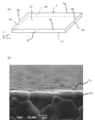
- FIG. 2 shows a piezoelectric ceramic plate, where (a) is a perspective view and (b) is a scanning electron microscope (SEM) photograph of the surface from the first side surface to the main surface.
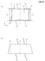
- (A) is explanatory drawing regarding the deformation
- (b) is explanatory drawing regarding the deformation amount of a piezoelectric ceramic plate whose main surface is a trapezoid.
- SEM scanning electron microscope
- FIG. 1A shows a piezoelectric ceramic plate 1 of the present embodiment.
- This piezoelectric ceramic plate 1 has a pair of rectangular shapes having a pair of substantially parallel sides 1a and a pair of other sides 1b facing each other. It has a main surface 1c, a pair of first side surfaces 1d facing each other, and a pair of second side surfaces 1e facing each other.
- the side on the main surface 1c side that constitutes the pair of first side surfaces 1d is the side 1a of the main surface 1c. Thereby, a pair of 1st side surfaces 1d are substantially parallel.
- FIG. 1B is an SEM photograph in which the surface of the piezoelectric ceramic plate 1 is observed obliquely from the main surface 1c so that the first side surface 1d and the main surface 1c can be confirmed.
- the baked surface is a surface that has not been processed after firing and is composed of crystal particles (ceramic particles) with rounded corners.
- the pair of second side surfaces 1e and the pair of main surfaces 1c are also baked surfaces, and the entire circumference is a baked surface.
- the length between the pair of first side surfaces 1d in the center of the length direction (x-axis direction) of the first side surface 1d is Lc, and the length direction of the first side surface 1d (
- the ratio ( ⁇ L / Lc) between the difference ⁇ L and Lc between Le and Lc is 1.0% or less.
- ⁇ L / Lc is 0.4% or less, further 0.2% or less, and further 0.1% or less.
- the difference ⁇ L is a value obtained by subtracting the shorter one from the longer one so as to be positive.
- the length between the first side surfaces 1d can be measured by, for example, a caliper or an image size measuring device (such as a CNC image measuring device).
- a straight line connecting both ends of one side 1a on the main surface 1c of the piezoelectric ceramic plate 1 is drawn, and both ends of the side 1a on this straight line are drawn.
- a perpendicular line C (one-dot chain line) is drawn with respect to the middle point, an intersection between the perpendicular line C and a pair of sides 1a on the main surface 1c is obtained, and a length between these intersections is defined as Lc.
- a line E that is located at either end of one side 1a and is parallel to the perpendicular C is drawn to obtain an intersection between the line E and the pair of sides 1a, and the length between these intersections is Le. .
- ⁇ L / Lc is 1.0% or less, so that it can be controlled to a predetermined shape and size without processing such as cutting and polishing, and can be easily and accurately shaped and dimensioned.
- the piezoelectric ceramic plate 1 can be obtained, and the manufacturing cost can be reduced.
- breakage such as chipping or cracking of the thin piezoelectric ceramic plate 1 can be reduced.
- FIG. 1 demonstrated the piezoelectric ceramic board 1 which has a pair of rectangular main surface 1c, as shown in FIG.2 (b), it is the piezoelectric ceramic board 1 which has a pair of trapezoid main surfaces 1c.
- Le and Lc draw a straight line connecting both ends of one of the shorter sides 1a of the pair of sides 1a of the main surface 1c, and a perpendicular C ( A one-dot chain line) is drawn, and a line E located at either end of one side 1a and parallel to the perpendicular C is drawn.
- the pair of main surfaces 1c are baked surfaces
- the baked surfaces may not be used. Since the pair of main surfaces 1c are also baked surfaces, the processing of the main surface 1c of the piezoelectric ceramic plate 1 after firing can be made unnecessary.
- the piezoelectric ceramic plate 1 has ( ⁇ L / Lc) of 1.0% or less even when the area of the main surface 1c is 360 mm 2 or more, and further, the area of the main surface 1c is 1000 mm 2 or more. Even in this case, it is preferable that ( ⁇ L / Lc) is 1.0% or less.
- the area of the main surface 1c can be calculated
- the ( ⁇ L / Lc) is 1.0 even when the piezoelectric ceramic plate 1 has an area of the main surface 1c and the thickness is 50 ⁇ m or less, and even 30 ⁇ m or less. % Or less is good.
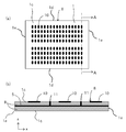
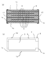
- FIG. 3 shows a first embodiment of an electronic component, which includes a plate-like substrate 8 having an internal electrode 5 in a piezoelectric ceramic plate 1.
- a plurality of surface electrodes 10 formed on the surface of the plate-like substrate 8 and the internal electrode 5 are connected to the internal electrodes 5 and extend in the thickness direction (z-axis direction) of the piezoelectric ceramic plate 1 and are drawn to the surface of the plate-like substrate 8. 11 and the pair of second side surfaces 1e of the piezoelectric ceramic plate 1 are baked surfaces.
- the first side surface 1d and the second side surface 1e of the piezoelectric ceramic plate 1 are baked surfaces, and the main surface 1c of the piezoelectric ceramic plate 1 is also a baked surface.
- the side surfaces 1d and 1e of the piezoelectric ceramic plate 1 are constituted by the side surfaces of the two piezoelectric layers 9, but cannot be confirmed from the appearance, and the side surfaces 1d and 1e of the piezoelectric ceramic plate 1 are integrally formed. It is composed. Since the boundary of the piezoelectric layer 9 is the internal electrode 5, the number of stacked piezoelectric layers 9 can be confirmed from the number of stacked internal electrodes 5.
- a voltage is applied between the surface electrode 10 and the internal electrode 5 via the via-hole conductor 11 drawn to the surface of the plate-like substrate 8 and the surface electrode 10.
- FIG. 3A the illustration of the via-hole conductor 11 is omitted.
- the size of the main surface 1c of the piezoelectric ceramic plate 1 is 360 mm 2 or more, more preferably 1000 mm 2 or more, and the thickness of the piezoelectric ceramic plate 1 having the internal electrode 5 is 150 ⁇ m or less, 100 ⁇ m or less, 60 ⁇ m or less, Furthermore, it is 50 ⁇ m or less.
- the distance between the pair of first side surfaces 1d of the piezoelectric ceramic plate 1 which is a baked surface is obtained by measuring with a caliper, an image dimension measuring device, or the like ( ⁇ L / Lc) is 1.0% or less.
- ⁇ L becomes several hundred ⁇ m or more by baking, and processing is necessary after firing.
- ⁇ L is 200 ⁇ m or less, and the length between the first side surfaces 1d after firing the piezoelectric ceramic plate 1 is ⁇ L / Lc of 1.0%. The following is satisfied and there is no need to process after firing. Therefore, since the electronic component of this embodiment is less deformed by firing, an electronic component having a desired shape and size can be obtained without being processed after firing, and the manufacturing cost can be reduced. In addition, cracks, chips and the like due to processing can be reduced.
- the electronic component may include three or more piezoelectric layers 9 and two or more internal electrodes 5.
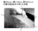
- FIG. 4 shows a state where an electronic component having a size of 35 mm ⁇ 116 mm and a thickness of 40 ⁇ m is held by a finger.
- FIG. 5 shows a second embodiment of the electronic component, and a pair of external electrodes arranged on the plate-like substrate 8 and the second side surface 1 e facing the piezoelectric ceramic plate 1 and alternately connected to the internal electrodes 5.
- a pair of second side surfaces 1e on which the external electrodes 17 of the piezoelectric ceramic plate 1 are disposed are processed surfaces. External electrodes 17 are arranged on these processed surfaces, and the internal electrodes 5 and the external electrodes 17 are connected.
- the processed surface is a surface obtained by processing the baked surface, such as a cut surface or a polished surface.
- the processed surface may be the entire pair of second side surfaces 1e of the piezoelectric ceramic plate 1, but, for example, the second side surface 1e of the second side surface 1e may be the second surface so that the portion where the external electrode 17 is disposed is used as the processed surface. It may be a part of the side surface 1e.
- the pair of first side surfaces 1d of the piezoelectric ceramic plate 1 on which the external electrodes 17 are not disposed are baked surfaces.
- the internal electrode 5 is a partial electrode formed on a part of the piezoelectric layer 9, and a part of the internal electrode 5 is the second side surface 1 e of the piezoelectric ceramic plate 1. And is connected to the external electrode 17.
- the length between the 1st side surfaces 1d of the piezoelectric ceramic board 1 which is a baking surface is satisfying
- the internal electrode 5 contains Ag as a main component, and in addition to Ag, Pd may be contained in a range of 35% by mass or less, and further 30% by mass or less.
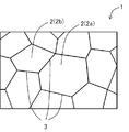
- the piezoelectric ceramic plate 1 (piezoelectric layer 9) includes a plurality of crystal particles 2 composed of lead zirconate titanate-based crystals (hereinafter also simply referred to as PZT-based crystals) containing Zn and Bi.
- a crystal grain boundary 3 existing between the crystal grains 2, and may be composed of the crystal grain 2 and the crystal grain boundary 3.
- the crystal grain boundaries 3 When the crystal grains 2 are subjected to local elemental analysis on the inside of the crystal grains 2 in the cross section of the piezoelectric ceramic plate 1 and a region including the crystal grain boundaries 3 (hereinafter sometimes referred to as the crystal grain boundaries 3), Zn and Bi As for at least one of these elements, when the content Ci in the crystal grain 2 and the content Cb on the crystal grain boundary 3 adjacent to the crystal grain 2 are compared, Ci is less than Cb. It is desirable to include (Ci ⁇ Cb) crystal particles 2.
- the crystal particle 2 in which Ci is less than Cb is referred to as first crystal particle 2a, and neither Zn nor Bi has a difference between Ci and Cb, or Ci is
- the crystal grains 2 that are larger than Cb (Ci ⁇ Cb) are referred to as second crystal grains 2b.
- the first crystal particle 2a is subjected to local elemental analysis on the contents of Zn and Bi with respect to the inside of the first crystal particle 2a and the crystal grain boundary 3 in contact with the first crystal particle 2a.
- the content of at least one of Zn and Bi is higher on the crystal grain boundary 3 than on the inside of the first crystal grain 2a.
- Such a piezoelectric ceramic plate 1 has a crystal phase (heterophase) other than an amorphous phase containing Li or B, which is a component that promotes sintering, or a PZT crystal, as in a conventional PZT piezoelectric ceramic plate. There is substantially no grain boundary 3. Therefore, the change with time of the insulation resistance and the deterioration of the piezoelectric characteristics due to these residuals are small.
- the contents of Zn and Bi inside the crystal grain 2 and on the crystal grain boundary 3 are determined by, for example, observing the cross section of the piezoelectric ceramic plate 1 with a scanning electron microscope (SEM) or a transmission electron microscope (TEM). Is obtained by conducting local elemental analysis of Zn and Bi on the grain boundary 3 adjacent to the crystal grain 2 and the inside thereof.
- SEM scanning electron microscope
- TEM transmission electron microscope
- Local elemental analysis can be performed using, for example, energy dispersive X-ray spectroscopy (EDS), field emission electron microanalyzer (FE-EPMA), Auger electron spectroscopy (AES), transmission electron microscope (TEM), and the like.
- EDS energy dispersive X-ray spectroscopy
- FE-EPMA field emission electron microanalyzer
- AES Auger electron spectroscopy
- TEM transmission electron microscope
- the contents of Zn and Bi inside the crystal particle 2 refer to the contents of Zn and Bi detected by elemental analysis of the center of the crystal particle 2 (the center of gravity of the cross section), for example, and the grain boundary 3
- the contents of Zn and Bi in the region containing mean the contents of Zn and Bi detected by elemental analysis of the crystal grain boundary 3 and the vicinity thereof.
- the above-described elemental analyzers have different spatial resolutions. For example, when a transmission electron microscope (TEM) is used, the spatial resolution is several nm, and when Auger electron spectroscopy (AES) is used, the spatial resolution is several. 10 nm. Therefore, even if measurement is performed on the crystal grain boundary 3, the measurement result of the crystal grain boundary 3 and its vicinity several nm (TEM) or several tens of nm (AES) and the measurement result at the center of the crystal grain 2 It becomes a comparison. Although the center of the crystal particle 2 (the center of gravity of the cross section) is given as the measurement location inside the crystal particle 2, the crystal grain boundary in the crystal particle 2 is used when an element analyzer with high spatial resolution such as TEM is used. You may analyze and evaluate the area
- the thickness of the crystal grain boundary 3 is 10 nm or less (about 1 to 5 nm), and the distance from the crystal grain boundary 3 is at least several in elemental analysis on the crystal grain boundary 3. It is considered that information in the vicinity of the crystal grain boundary 3 of the crystal grain 2 that is the inside of the crystal grain 2 of nm, that is, the very surface of the crystal grain 2 is included.
- the first crystal particle 2 a in the piezoelectric ceramic plate 1 of the present embodiment has a layer rich in at least one of Zn and Bi in the very vicinity of the crystal grain boundary 3 (near the surface of the crystal particle 2). And the thickness of the layer is considered to be several nm. Therefore, in this specification, the region including the crystal grain boundary 3 includes the surface layer of the crystal grain 2 within a range of several nm from the crystal grain boundary 3.
- the elemental analysis is performed by measuring at least one point inside the crystal particle 2 and the crystal grain boundary 3 (a grain boundary between the two faces) closest to the measurement point inside the crystal particle 2. Alternatively, it may be performed for one point in a region including a triple point) and the results may be compared.
- the ratio of Cb (Zn) to Ci (Zn) (Cb (Zn) / Ci (Zn)) is preferably 1.04 or more and 2.0 or less in terms of mass ratio.
- the ratio of Cb (Bi) to Ci (Bi) (Cb (Bi) / Ci (Bi)) is preferably 1.03 or more, more preferably 1.05 or more in terms of mass ratio. By setting it as such a ratio, it becomes possible to densify at low temperature. Further, (Cb (Bi) / Ci (Bi)) is preferably 2.0 or less, particularly 1.8 or less in terms of mass ratio.
- the ratio of the first crystal particles 2a in the crystal particles 2 constituting the piezoelectric ceramic plate 1 is the total number of the first crystal particles 2a and the second crystal particles 2b (hereinafter referred to as the number of crystal particles 2). ) To the number of the first crystal grains 2a is preferably 80% or more. By setting the ratio of the first crystal particles 2a to 80% or more, more preferably 90% or more, the piezoelectric ceramic plate 1 with little deformation even when densified with a thin shape and with few amorphous phases and different phases, become.
- the proportion of the first crystal particles 2a and the second crystal particles 2b occupied by the first crystal particles 2a is determined by measuring the cross section of the piezoelectric ceramic plate 1 with a scanning electron microscope (SEM) or transmission electron. At least 10 arbitrary crystal particles 2 are extracted by observation with a microscope (TEM), and local elemental analysis of Zn and Bi is performed inside the crystal particles 2 and at the crystal grain boundaries 3 adjacent to the crystal particles 2, The ratio of the number of first crystal particles 2a to the number of measured crystal particles 2 may be calculated.
- SEM scanning electron microscope
- TEM microscope
- the piezoelectric ceramic plate 1 of the present embodiment is composed of PZT-based crystal grains 2 and crystal grain boundaries 3 existing between the crystal grains 2 in terms of maintaining stable insulation resistance and piezoelectric characteristics, and other than PZT-based crystals. It is preferable that the crystal phase, that is, a crystal phase with low piezoelectric characteristics and insulation resistance is substantially not included.
- a crystal phase other than the PZT crystal hereinafter referred to as “different phase”
- TEM transmission electron microscope
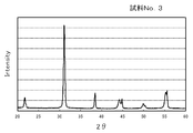
- Cuk ⁇ in the cross section of the piezoelectric ceramic plate 1.
- the fact that a peak derived from a different phase other than the PZT crystal does not substantially exist means that the (111) diffraction peak intensity of the PZT crystal is 100. Means that the diffraction peak intensity is 3 or less.
- the diffraction peak intensity is represented by the length to the peak perpendicular to the tangent line, with tangent lines drawn on both sides of the diffraction peak in the diffraction profile obtained by X-ray diffraction (XRD) measurement.
- the peak intensity of the crystal phase (heterophase) other than the PZT crystal phase with low piezoelectric characteristics and insulation resistance is the (111) diffraction peak of the PZT crystal. If it is 3 or less with respect to strength, it can be suitably used without greatly affecting the piezoelectric characteristics of the piezoelectric ceramic plate 1.
- the piezoelectric ceramic plate 1 of the present embodiment does not substantially contain alkali metal elements such as Li and Na and B (boron).
- alkali metal elements such as Li or Na and B (boron)
- a liquid phase is formed and the sinterability is improved.
- an amorphous phase or a crystal phase other than the PZT crystal remains in the boundary 3 and the insulation resistance is lowered with time or the piezoelectric characteristics are lowered.
- alkali metal elements such as Li and Na and B (boron) may be inevitably contained as impurities in the piezoelectric ceramic plate 1. Therefore, substantially not containing alkali metal elements such as Li and Na and B (boron) means that these elements are not actively added in the manufacturing process of the piezoelectric ceramic plate 1.
- the porosity of the piezoelectric ceramic plate 1 of this embodiment is 0.25% or less from the point of denseness. In this manner a dense piezoelectric ceramic plate 1, the density becomes a 7.7 g / cm 3 or more and still more 7.8 g / cm 3 or more, it is possible to reduce the mechanical loss, Ya degradation of piezoelectric characteristics The piezoelectric ceramic plate 1 has little variation.
- the average particle diameter of the crystal particles 2 in the piezoelectric ceramic plate 1 of the present embodiment is preferably 1.0 to 4.0 ⁇ m. If the average particle size of the crystal particles 2 is too small, the piezoelectric characteristics are deteriorated. If the average particle size is too large, the hysteresis is increased, and heat is easily generated when driven as an electronic component. By setting the average particle size of the crystal particles 2 in the range of 1.0 to 4.0 ⁇ m, it is possible to maintain necessary piezoelectric characteristics and to suppress heat generation when driven as an electronic component.
- the piezoelectric ceramic plate 1 includes crystal grains 2 made of a lead zirconate titanate crystal containing Zn and Bi, and crystal grain boundaries 3.
- the crystal particle 2 is a composite perovskite type compound, and preferably contains Sb, Cu, Ni, Nb in addition to Pb, Zr, Ti, Zn, and Bi as a metal component, and if necessary, at least of Sr and Ba. It is desirable to include any one of them.
- the composition of the piezoelectric ceramic plate 1 is represented by a first component represented by the following composition formula and a second component composed of Bi oxide and Zn oxide.
- M represents at least one element of Cu and Ni.
- x, y, a, b, and c satisfy the following relational expressions.
- ⁇ is 0.1 or more and 2.0 or less.
- ⁇ is the total amount of Zn and Bi as the second component in terms of oxides (ZnO and Bi 2 O 3 ), respectively, but is a complex oxide of Zn and Bi, such as Bi 38 ZnO 58 , Bi 38 ZnO 60. , Bi 48 ZnO 73, BiZnO and the like.
- the ratio of Zn to Bi (Bi / Zn) in the second component is preferably 1 ⁇ (Bi / Zn) ⁇ 48 in terms of element ratio.
- the reason why x, y, a, b, c, and ⁇ are set in the above ranges will be described.
- the reason why the substitution amount x of Pb with Sr is set to 0 ⁇ x ⁇ 0.14 is that the Curie temperature can be kept high by substituting a part of Pb with Sr.
- the reason why the substitution amount y of Pb with Ba is set to 0 ⁇ y ⁇ 0.14 is that the Curie temperature can be kept high by replacing a part of Pb with Ba, and a high piezoelectric strain constant d 31 can be obtained. Because it can.
- the reason why the substitution amount a of Ti with (Zn 1/3 Sb 2/3 ) is set to 0.01 ⁇ a ⁇ 0.12 is that a large piezoelectric strain constant d 31 and a piezoelectric output constant g 31 are obtained. This is because the temperature can be kept high and the dielectric loss can be kept small.
- a large piezoelectric strain constant can be obtained by setting 0.05 ⁇ a ⁇ 0.12, and 0.01% when used as a piezoelectric sensor. By setting ⁇ a ⁇ 0.05, a large piezoelectric output constant g 31 can be obtained.
- the coercive electric field can be increased while suppressing the decrease in the piezoelectric d constant.
- Ni and Cu are used as M, but when Cu is used, the piezoelectric ceramic plate 1 having a large coercive electric field can be obtained while maintaining a particularly high piezoelectric d constant, and deterioration of displacement can be suppressed.
- b is particularly preferably 0.002 ⁇ b ⁇ 0.01.
- the piezoelectric ceramic plate 1 containing PZT as a main component has MPB (Morphotropic phase boundary) that shows the maximum value of the piezoelectric strain constant when the solid solution ratio of PbZrO 3 and PbTiO 3 is changed.
- MPB Mophotropic phase boundary
- this MPB and the composition in the vicinity thereof are used. Since this MPB varies depending on the values of x, y, a, and b, the value of c is set to a composition range in which MPB can be captured within the composition ranges of x, y, a, and b.
- the mass ratio ⁇ (%) of the second component (Zn oxide and Bi oxide) to the first component was set to 0.1 ⁇ ⁇ ⁇ 2.0.
- the Bi oxide forms a liquid phase at the time of firing to wet the crystal particles 2 that are PZT-based crystals, improves the sinterability, and uniformly sinters the entire porcelain. This is because warpage and deformation can be reduced even in the piezoelectric ceramic plate 1, and after sintering, Zn and Bi can be dissolved in the PZT crystal to improve the piezoelectric characteristics.
- the ratio of Zn to Bi (Bi / Zn) is preferably 1 ⁇ (Bi / Zn) ⁇ 48 in terms of element ratio. By setting it as such a ratio, a 2nd component forms a liquid phase at low temperature, and the uniform sintering of the whole ceramic becomes possible.
- the piezoelectric ceramic plate 1 of the present embodiment can be manufactured as follows. For example, a mixed raw material of a calcined powder of a PZT crystal containing the first component and a powder containing the second component (Bi oxide and Zn oxide) is formed by a well-known sheet forming method, and is 900 in the atmosphere. Bake at ⁇ 1050 ° C.
- the electronic component forms an internal electrode pattern by applying an internal electrode paste to the green sheet. A plurality of green sheets on which internal electrode patterns are formed are laminated, and finally a green sheet on which no internal electrode pattern is formed is laminated to produce a plate-like substrate molded body. Bake at 900-1050 ° C.
- the second component (Bi oxide and Zn oxide) is baked at a low temperature of 900 to 1050 ° C.
- the second component (Bi oxide and Zn oxide) forms a liquid phase at a low temperature of about 750 ° C., for example.
- the PZT crystal grains 2 can be sufficiently wetted at a temperature lower than the firing temperature, thereby improving the sinterability, and the piezoelectric ceramic plate 1 as a whole contracts almost uniformly and is sintered. Later, Bi and Zn are dissolved in the PZT crystal.
- the sintered piezoelectric ceramic plate 1 is composed of crystal grains 2 of PZT crystal, and the crystal grains 2 contain the first crystal grains 2a. desirable.
- a calcination powder of PZT crystal containing Zn is prepared.
- PbO, ZrO 2 , TiO 2 and ZnO powders as raw materials, and optionally Sb 2 O 3 , CuO, NiO, Nb 2 O 5 , SrCO 3 and BaCO 3 powders as necessary.
- the mixture is dehydrated and dried, and calcined at a maximum temperature of 850 to 950 ° C. for 1 to 3 hours.
- the obtained calcined powder of PZT crystal is a calcined powder composed of the first component.
- the obtained calcined powder is pulverized again with a ball mill or the like so that, for example, the average particle diameter D 50 is in the range of 0.5 to 0.7 ⁇ m.
- the degree of synthesis of the PZT crystal it is preferable to appropriately adjust the degree of synthesis of the PZT crystal.
- an index representing the PZT-based crystal using a peak intensity I 2 of the peak intensity I 1 of the peak of the PZT-based crystal (101) (2 ⁇ ⁇ 30 ° ), and the peak of (111) (2 ⁇ ⁇ 38 ° ).
- I 2 / I 1 is the intensity ratio I 1 of I 2 is preferably set to 0.130 to 0.160.
- the synthesis of the PZT-based crystal has progressed appropriately, and the second component (Zn oxide and Bi oxide) Addition improves the sinterability. Further, simultaneously with the grain growth in the sintering stage, Zn and Bi are taken into the surface layer of the PZT-based crystal and sintered without remaining as a liquid phase component in the temperature range of 900 to 1050 ° C.
- the peak intensity I 1 of the peak of the (101) of the PZT-based crystal (2 [Theta] ⁇ 30 °), (111) is to use a peak intensity I 2 of the peak (2 [Theta] ⁇ 38 °) of other peaks synthesis of The peak position and pattern shape change with the change of (crystal phase), whereas the peak of (101) (2 ⁇ 30 °) and the peak of (111) (2 ⁇ 38 °) change even if the degree of synthesis changes. This is because only the intensity ratio changes and the peak position and pattern shape do not change, and it is considered optimal for expressing the degree of synthesis of the PZT crystal.
- the powder of the second component Zn oxide and Bi oxide, such as ZnO and Bi 2 O 3
- each powder may be added to the calcined powder, or a mixed powder obtained by mixing only the second component in advance may be added to the calcined powder.
- the second component may be calcined to synthesize a composite oxide containing Zn and Bi (hereinafter referred to as BZ oxide) and added to the calcined powder.
- BZ oxide composite oxide containing Zn and Bi
- the average particle diameter D 50 of the second component is in the range of 0.5 to 0.7 ⁇ m, particularly using a ball mill or the like so as to be smaller than the average particle diameter (D 50 ) of the calcined powder of PZT-based crystals. It is preferable to adjust.
- the calcined powder of the PZT-based crystal to which the second component has been added is mixed with a binder and then formed into a desired shape using a known forming method such as press forming or sheet forming such as a doctor blade method.
- the formed body is fired at 900 to 1050 ° C. in the air.
- Li, B, and the like that form a liquid phase have been added in order to fire a PZT crystal at a low temperature.
- the piezoelectric ceramic plate 1 using such an additive although it can be fired at a low temperature, there is an amorphous phase or a crystal phase other than the PZT crystal at the grain boundary of the PZT crystal grain, and the insulation resistance is deteriorated over time. Or the piezoelectric characteristics have deteriorated.
- Bi 2 O 3 is used as a solid solution in the PZT crystal, the liquid phase generation temperature is relatively high at about 820 ° C., so that it is difficult to uniformly sinter the entire porcelain. In the piezoelectric ceramic plate, warpage and deformation occurred.
- the piezoelectric ceramic plate 1 of the present embodiment even if the piezoelectric ceramic plate 1 is fired at a low temperature of 900 to 1050 ° C., the Zn oxide and Bi oxide as the second component form a liquid phase and wet the crystal particles 2 of the PZT crystal. Therefore, the sinterability is high, the porosity is 0.25% or less, and the density is 7.7 g / cm 3 or more. Furthermore, after sintering, the piezoelectric ceramic plate 1 in which Zn and Bi forming a liquid phase are dissolved in the surface layer of the crystal grains 2 of the PZT crystal and the thickness of the crystal grain boundary 3 is 10 nm or less (about 1 to 5 nm). It becomes.
- the piezoelectric ceramic plate 1 has a content of at least any one element of Zn and Bi in the first crystal particles 2a, that is, in the PZT-based crystal particles 2 than in a region including the crystal grain boundaries 3.
- the first crystal particle 2a with a small number, in other words, a first layer having a layer rich in at least one of Zn and Bi in the vicinity of the crystal grain boundary 3 of the PZT-based crystal particle 2 (surface layer of the crystal particle 2). Crystal grains 2a.
- the piezoelectric ceramic plate 1 includes a plurality of PZT crystal grains 2 and crystal grain boundaries 3 existing between the crystal grains 2, and the crystal grains 2 include first crystal grains 2 a.
- the crystal grain boundary 3 is substantially free from crystal phases and amorphous phases other than the PZT crystal, and has excellent piezoelectric characteristics.
- the volume resistivity becomes 1 G ⁇ ⁇ m or more even after 100 hours have passed at 85 ° C., and insulation deterioration during continuous driving can be suppressed.
- the second component generates a liquid phase at about 750 ° C., and the entire porcelain starts sintering uniformly during firing. Therefore, even if the shape is thin, the piezoelectric ceramic plate 1 is hardly deformed during the sintering process.
- the piezoelectric ceramic plate 1 of the present embodiment is suitably used for an electronic component having a thickness of 150 ⁇ m or less, particularly 50 ⁇ m or less.
- the piezoelectric ceramic plate 1 can be used as various electronic components such as a ceramic filter, an ultrasonic application vibrator, a piezoelectric buzzer, a piezoelectric ignition unit, an ultrasonic motor, a piezoelectric fan, a piezoelectric sensor, and a piezoelectric actuator.
- a piezoelectric actuator uses a displacement or force generated through a piezoelectric phenomenon as a mechanical drive source, and is one of those that have recently attracted attention in the field of mechatronics.
- Piezoelectric actuators are solid-state elements that use the piezoelectric effect and consume less power, have a faster response speed, have a larger amount of displacement, and generate heat compared to conventional electromagnetic actuators that have a configuration in which a coil is wound around a magnetic material. It has excellent features such as small amount, small size and weight.
- a laminated piezoelectric actuator capable of obtaining a larger displacement and generating force at a lower voltage has been put to practical use as an acoustic component such as an autofocus for a camera for opening / closing a fuel injection valve of an in-vehicle injector and a piezoelectric speaker.
- a powder of PbO, ZrO 2 , TiO 2 , ZnO, Sb 2 O 3 , SrCO 3 , BaCO 3 , CuO, Nb 2 O 5 is used as a raw material powder, and the first component is a composition formula Pb 1-xy Sr x were weighed so as to have the composition shown in Table 1 in Ba y Ti 1-a-b -c (Zn 1/3 Sb 2/3) a (M 1/3 Nb 2/3) b Zr c O 3, in a ball mill For 24 hours. M is Cu or Ni. Next, this mixture is dehydrated and dried, and then calcined at the calcining temperature shown in Table 1 for 3 hours. The calcined product is wet-ground again with a ball mill for 24 hours, and the D 50 is 0.5 to 0.7 ⁇ m. A baked powder was obtained.
- the additive shown in Table 1 having a D 50 of 0.5 to 0.7 ⁇ m is added in an amount (% by mass) shown in Table 1 in a ratio to 100% by mass of the first component, and an organic binder is mixed therewith.
- a green sheet having a thickness of 30 ⁇ m was prepared by a doctor blade method.
- the internal electrode paste containing Ag and Pd was screen-printed, 15 green sheets on which the internal electrode paste was printed were stacked, and finally the green sheet on which the internal electrode paste was not printed was stacked.
- a plate-like substrate molded body was produced.
- An external electrode was formed by baking Ag paste on both end faces of the obtained plate-like substrate, and polarization treatment was performed to obtain a laminated piezoelectric actuator which is an electronic component for evaluating piezoelectric characteristics.
- the thickness of one piezoelectric layer of the piezoelectric ceramic plate was 25 ⁇ m.
- the porosity of the piezoelectric layer was obtained by mirror-polishing the cross section of the plate-shaped substrate, observing the polished surface using a scanning electron microscope (SEM), and processing the photograph of the piezoelectric layer. .
- SEM scanning electron microscope
- the SEM photograph of the polished surface that was subjected to thermal etching treatment in the atmosphere, at 950 ° C. for 3 hours was subjected to image processing, and the equivalent circle diameter of the cross-sectional area obtained from the contour of the crystal particle constituting the piezoelectric layer was crystal grain
- the average particle diameter of crystal grains in the piezoelectric layer was determined.
- the density of the piezoelectric layer the bulk density of the plate-like substrate was obtained by the Archimedes method, and the bulk density was regarded as the density of the piezoelectric layer.
- the composition of the plate-like substrate was confirmed by ICP emission spectroscopic analysis, the composition of the piezoelectric layer was in agreement with the composition at the time of preparation within an error range.
- Whether or not there is a crystal phase other than the PZT crystal in the piezoelectric layer of the piezoelectric ceramic plate is determined by X-ray diffraction (XRD) measurement using Cuk ⁇ rays of the plate-like substrate other than the PZT crystal peak. When there was substantially no peak due to the crystal, it was judged that there was no crystal phase other than the PZT crystal.
- Sample No. The X-ray diffraction measurement result of No. 3 is shown in FIG.
- the X-ray diffraction measurement result of No. 5 is shown in FIG.
- a plate-like substrate for measuring deformation was prepared.
- a green sheet having a thickness of 25 ⁇ m was prepared by a doctor blade method, and the internal electrode paste was printed on the entire area of 14.8 ⁇ 28 mm on the green sheet using the internal electrode paste.
- a green sheet on which the internal electrode paste was not printed was overlaid on the printing surface side of the green sheet on which the internal electrode paste was printed, and after removing the binder, firing was performed to obtain a plate-like substrate.
- the firing conditions were the same as the conditions for producing the laminated piezoelectric actuator.
- the thickness of the obtained plate-like substrate was 42 ⁇ m (the thickness of the piezoelectric layer was 21 ⁇ m), and was a rectangular plate having a main surface area of 360 mm 2 .
- the deformation of the piezoelectric ceramic plate was evaluated as a ratio ( ⁇ L / Lc).
- the length of the piezoelectric ceramic plate was measured using a CNC image measuring device. The results are shown in Table 1.
- the porosity is densified to 0.25% or less even when fired at a low temperature, and the piezoelectric characteristics are as high as 250 p ⁇ m / V or more in terms of the piezoelectric strain constant d 31.
- the initial volume resistivity was 80 G ⁇ ⁇ m or more, and even after 100 hours had passed at 85 ° C., the volume resistivity was 70 G ⁇ ⁇ m or more, and the deterioration of the insulation resistance with time was small, and the deformation of the piezoelectric ceramic plate was also small.
- the deformation ratio is smaller than 0.1%.
- the sample containing Cu in the piezoelectric layer had a higher coercive electric field than the sample containing no Cu having the same composition while maintaining a high piezoelectric d constant.
- a first component was prepared, a second component was added to the first component, an organic binder was mixed therein, and then a green sheet was prepared by a doctor blade method. After applying the internal electrode paste over the entire area of the green sheet, and overlaying the green sheet without the internal electrode paste on the printing surface side of the green sheet with the internal electrode paste applied, and performing the binder removal Then, a plate-like substrate having a laminated structure as shown in FIG. 3 having the thickness of the piezoelectric ceramic plate, the area of the main surface of the piezoelectric ceramic plate, and the thickness of the piezoelectric layer shown in Table 2 was produced.
- FIG. 5 A plate-like substrate as shown in FIG. 5 was produced.
Landscapes
- Engineering & Computer Science (AREA)
- Chemical & Material Sciences (AREA)
- Manufacturing & Machinery (AREA)
- Ceramic Engineering (AREA)
- Materials Engineering (AREA)
- Structural Engineering (AREA)
- Organic Chemistry (AREA)
- Inorganic Chemistry (AREA)
- Composite Materials (AREA)
- Physics & Mathematics (AREA)
- Thermal Sciences (AREA)
- Compositions Of Oxide Ceramics (AREA)
Abstract
Description
図1(a)は、本実施形態の圧電磁器板1を示すもので、この圧電磁器板1は、対向するほぼ平行な一対の辺1a、他の一対の辺1bを有する長方形状の一対の主面1cと、対向する一対の第1側面1dおよび対向する一対の第2側面1eを有している。一対の第1側面1dを構成する主面1c側の辺は、主面1cの辺1aである。これにより、一対の第1側面1dはほぼ平行となっている。
図3は、電子部品の第1の実施形態を示すもので、この電子部品は、圧電磁器板1内に内部電極5を有する板状基体8を具備している。そして、板状基体8表面に複数形成された表面電極10と、内部電極5に接続され、圧電磁器板1の厚み方向(z軸方向)に延びて板状基体8表面に引き出されたビアホール導体11とを具備するとともに、圧電磁器板1は、一対の第2側面1eがそれぞれ焼き上げ面である。
圧電磁器板1(圧電体層9)は、図6に示すように、ZnおよびBiを含むチタン酸ジルコン酸鉛系結晶(以下、単にPZT系結晶ともいう)からなる複数の結晶粒子2と、結晶粒子2間に存在する結晶粒界3と、を有するものであり、結晶粒子2と結晶粒界3とからなるものであってもよい。
第1成分:Pb1-x-ySrxBayTi1-a-b-c(Zn1/3Sb2/3)a(M1/3Nb2/3)bZrcO3
なお、第1成分の組成式において、x、y、a、b、cは、以下の関係式を満たす。
0≦y≦0.14(ただし、x+y≧0.04)、
0.01≦a≦0.12、
0≦b≦0.015
0.42≦c≦0.58、
また、第1成分100質量%に対する第2成分の質量比をα%と表したとき、αは0.1以上2.0以下である。なお、αは第2成分であるZnおよびBiをそれぞれ酸化物換算(ZnOおよびBi2O3)した合量とするが、ZnとBiの複合酸化物、たとえばBi38ZnO58、Bi38ZnO60、Bi48ZnO73およびBiZnOなどに換算した量であってもよい。第2成分中におけるZnとBiとの比率(Bi/Zn)は、元素比率にして1≦(Bi/Zn)≦48とすることが好ましい。
本実施形態の圧電磁器板1は、以下のようにして作製することができる。例えば、第1成分を含むPZT系結晶の仮焼粉末と、第2成分(Bi酸化物およびZn酸化物)を含む粉末との混合原料を、周知のシート成形法で成形し、大気中で900~1050℃で焼成する。また、電子部品は、上記グリーンシートに内部電極ペーストを塗布して内部電極パターンを形成する。内部電極パターンが形成されたグリーンシートを複数積層し、最後に内部電極パターンが形成されていないグリーンシートを積層して板状基体成形体を作製し、この板状基体成形体を、大気中で900~1050℃で焼成する。


1c・・・主面
1d・・・第1側面
1e・・・第2側面
2・・・結晶粒子
5・・・内部電極
7・・・外部電極
8・・・板状基体
Claims (10)
- 一対の四角形状の主面と、対向する一対の第1側面および対向する一対の第2側面とを有し、前記一対の第1側面が焼き上げ面であるとともに、前記第1側面の長さ方向中央における前記一対の第1側面間の長さをLcとし、前記第1側面の長さ方向端における前記一対の第1側面間の長さをLeとしたとき、該Leと前記Lcとの差ΔLと前記Lcとの比率(ΔL/Lc)が1.0%以下であることを特徴とする圧電磁器板。
- 前記一対の主面が焼き上げ面であることを特徴とする請求項1に記載の圧電磁器板。
- 前記一対の第1側面は、角が丸くなった結晶粒子で構成されている請求項1または2に記載の圧電磁器板。
- 前記主面の面積が360mm2以上であることを特徴とする請求項1乃至3のうちいずれかに記載の圧電磁器板。
- 前記主面の面積が1000mm2以上である請求項1乃至4のうちいずれかに記載の圧電磁器板。
- 一対の四角形状の主面と、対向する一対の第1側面および対向する一対の第2側面とを有し、前記主面の面積が360mm2以上であるとともに、前記一対の第1側面が焼き上げ面であることを特徴とする圧電磁器板。
- 厚みが150μm以下であることを特徴とする請求項1乃至6のうちいずれかに記載の圧電磁器板。
- 請求項1乃至7のうちいずれかに記載の圧電磁器板内に内部電極を有することを特徴とする板状基体。
- 請求項8に記載の板状基体の表面に配置された表面電極と、前記内部電極に接続され、前記圧電磁器板の厚み方向に延びて前記板状基体の表面に引き出されたビアホール導体とを具備するとともに、前記圧電磁器板は、前記一対の第2側面が焼き上げ面であることを特徴とする電子部品。
- 請求項8に記載の板状基体と、前記圧電磁器板の第2側面に配置され、前記内部電極に接続された外部電極とを具備するとともに、前記圧電磁器板の第2側面に加工面を有し、該加工面に前記外部電極が配置されていることを特徴とする電子部品。
Priority Applications (4)
| Application Number | Priority Date | Filing Date | Title |
|---|---|---|---|
| US15/032,422 US10297744B2 (en) | 2014-08-29 | 2015-08-29 | Piezoelectric ceramic plate, plate-shaped substrate and electronic component |
| JP2016507940A JP6082161B2 (ja) | 2014-08-29 | 2015-08-29 | 圧電磁器板および板状基体ならびに電子部品 |
| CN201580002390.9A CN105683128B (zh) | 2014-08-29 | 2015-08-29 | 压电陶瓷板以及板状基体、和电子部件 |
| EP15835045.4A EP3085677B1 (en) | 2014-08-29 | 2015-08-29 | Piezoelectric ceramic plate, plate-shaped substrate and electronic component |
Applications Claiming Priority (2)
| Application Number | Priority Date | Filing Date | Title |
|---|---|---|---|
| JP2014175767 | 2014-08-29 | ||
| JP2014-175767 | 2014-08-29 |
Publications (1)
| Publication Number | Publication Date |
|---|---|
| WO2016031994A1 true WO2016031994A1 (ja) | 2016-03-03 |
Family
ID=55399875
Family Applications (2)
| Application Number | Title | Priority Date | Filing Date |
|---|---|---|---|
| PCT/JP2015/074549 Ceased WO2016031994A1 (ja) | 2014-08-29 | 2015-08-29 | 圧電磁器板および板状基体ならびに電子部品 |
| PCT/JP2015/074551 Ceased WO2016031995A1 (ja) | 2014-08-29 | 2015-08-29 | 圧電磁器およびその製法、ならびに電子部品 |
Family Applications After (1)
| Application Number | Title | Priority Date | Filing Date |
|---|---|---|---|
| PCT/JP2015/074551 Ceased WO2016031995A1 (ja) | 2014-08-29 | 2015-08-29 | 圧電磁器およびその製法、ならびに電子部品 |
Country Status (5)
| Country | Link |
|---|---|
| US (2) | US10177300B2 (ja) |
| EP (2) | EP3085678B1 (ja) |
| JP (3) | JP6082161B2 (ja) |
| CN (2) | CN105683128B (ja) |
| WO (2) | WO2016031994A1 (ja) |
Cited By (1)
| Publication number | Priority date | Publication date | Assignee | Title |
|---|---|---|---|---|
| WO2020045095A1 (ja) * | 2018-08-30 | 2020-03-05 | 株式会社村田製作所 | 第1段階セラミック集合基板、第2段階セラミック集合基板、第2段階セラミック集合基板の製造方法、および、積層電子部品の製造方法 |
Families Citing this family (5)
| Publication number | Priority date | Publication date | Assignee | Title |
|---|---|---|---|---|
| US11699985B2 (en) | 2017-10-12 | 2023-07-11 | Sumitomo Electric Industries, Ltd. | Layered body, and saw device |
| CN111194299A (zh) * | 2017-10-12 | 2020-05-22 | 住友电气工业株式会社 | 陶瓷基板、层状体和saw器件 |
| CN110412091B (zh) * | 2019-07-10 | 2024-04-23 | 宁波大学 | 一种可重复使用的损伤识别压电传感装置 |
| JP7672195B2 (ja) * | 2019-09-27 | 2025-05-07 | 太陽誘電株式会社 | コイル部品、回路基板及び電子機器 |
| WO2024233964A1 (en) * | 2023-05-10 | 2024-11-14 | Quest Integrity Usa, Llc | Lead zirconate titanate (pzt) solution phase diagram and crystal growth near thermodynamic equilibrium |
Citations (5)
| Publication number | Priority date | Publication date | Assignee | Title |
|---|---|---|---|---|
| JPH04298085A (ja) * | 1991-03-26 | 1992-10-21 | Kyocera Corp | 圧電性磁器の製造方法 |
| JPH04325464A (ja) * | 1991-04-25 | 1992-11-13 | Tokin Corp | 圧電セラミックスの焼成方法 |
| JPH0555661A (ja) * | 1991-08-26 | 1993-03-05 | Kyocera Corp | 圧電磁器の製造方法 |
| WO2004026789A1 (ja) * | 2002-09-18 | 2004-04-01 | Tdk Corporation | 圧電磁器組成物、圧電素子及びこれらの製造方法 |
| JP2010222170A (ja) * | 2009-03-23 | 2010-10-07 | Nec Tokin Corp | 積層圧電セラミックス体の製造方法 |
Family Cites Families (27)
| Publication number | Priority date | Publication date | Assignee | Title |
|---|---|---|---|---|
| JP2531270B2 (ja) | 1989-07-24 | 1996-09-04 | 日本電気株式会社 | 厚み振動圧電磁器トランスの製造方法 |
| DE4127829C2 (de) * | 1991-08-22 | 1994-05-19 | Renate Prof Dr Ing Gesemann | PZT - Werkstoffe und deren Verwendung |
| JP3210782B2 (ja) | 1993-07-29 | 2001-09-17 | 京セラ株式会社 | アクチュエータ用圧電磁器組成物 |
| DE4427798C2 (de) * | 1993-08-06 | 1998-04-09 | Toshiba Kawasaki Kk | Piezoelektrischer Einkristall und dessen Verwendung in einer Ultraschallsonde und Ultraschall-Array-Sonde |
| DE19615695C1 (de) * | 1996-04-19 | 1997-07-03 | Siemens Ag | Verfahren zur Herstellung eines Piezoaktors monolithischer Vielschichtbauweise |
| JP2970652B1 (ja) * | 1998-05-22 | 1999-11-02 | 松下電器産業株式会社 | 積層セラミック部品およびその製造方法 |
| JP2000086341A (ja) | 1998-09-11 | 2000-03-28 | Kyocera Corp | 圧電磁器組成物及びその製造方法 |
| JP2001111127A (ja) * | 1999-10-04 | 2001-04-20 | Kyocera Corp | 圧電/電歪型アクチュエータ及びその製造方法 |
| US7354642B2 (en) * | 2000-02-16 | 2008-04-08 | Taiyo Yuden Co., Ltd. | Multilayer displacement element |
| JP3506113B2 (ja) | 2000-11-07 | 2004-03-15 | 株式会社村田製作所 | 電子部品 |
| JP5013653B2 (ja) * | 2003-06-30 | 2012-08-29 | 京セラ株式会社 | 圧電アクチュエータの製造方法 |
| CN1304334C (zh) * | 2004-05-24 | 2007-03-14 | Tdk株式会社 | 氧化锆装载板、陶瓷基片的制造方法 |
| JP2006256925A (ja) * | 2005-03-18 | 2006-09-28 | Taiheiyo Cement Corp | 圧電セラミックス用焼結助剤および圧電セラミックス |
| CN101547875B (zh) * | 2007-02-07 | 2012-08-22 | 株式会社村田制作所 | 压电陶瓷及压电元件 |
| US7948153B1 (en) | 2008-05-14 | 2011-05-24 | Sandia Corporation | Piezoelectric energy harvester having planform-tapered interdigitated beams |
| JP5361635B2 (ja) * | 2008-09-25 | 2013-12-04 | 京セラ株式会社 | 振動体 |
| JP5597368B2 (ja) | 2009-07-29 | 2014-10-01 | 京セラ株式会社 | 積層型電子部品およびその製法 |
| JP5530140B2 (ja) * | 2009-09-28 | 2014-06-25 | 太平洋セメント株式会社 | Bnt−bt系圧電セラミックスおよびその製造方法 |
| CN101712548B (zh) * | 2009-09-30 | 2012-10-17 | 广州市番禺奥迪威电子有限公司 | 一种烧结温度低的高效压电陶瓷材料及其制备工艺 |
| JP5468984B2 (ja) * | 2010-05-17 | 2014-04-09 | 太平洋セメント株式会社 | 非鉛圧電セラミックス用焼結助剤、非鉛圧電セラミックスおよびその製造方法 |
| JP5847803B2 (ja) | 2011-03-30 | 2016-01-27 | 日本碍子株式会社 | 圧電体基板の製造方法 |
| CN102432291B (zh) * | 2011-09-04 | 2014-05-28 | 成都宏明电子科大新材料有限公司 | 电容正电压系数反铁电陶瓷材料及其制作方法 |
| DE102011117709A1 (de) * | 2011-11-04 | 2013-05-08 | Epcos Ag | Keramikmaterial, Verfahren zur Herstellung desselben und elektrokeramisches Bauelement umfassend das Keramikmaterial |
| CN102531638B (zh) | 2012-01-05 | 2013-11-20 | 江苏大学 | 一种添加物及其降低压电陶瓷烧结温度的用途 |
| JP5855509B2 (ja) * | 2012-03-30 | 2016-02-09 | 日本碍子株式会社 | 圧電/電歪膜型素子及び圧電/電歪膜型素子を製造する方法 |
| EP2833424A4 (en) * | 2012-03-30 | 2015-11-11 | Ngk Insulators Ltd | PIEZOELECTRIC / ELECTROSTRICTIVE FILM TYPE ELEMENT, AND METHOD FOR PRODUCTION OF PIEZOELECTRIC / ELECTROSTRICTIVE FILM TYPE ELEMENT |
| CN103090661B (zh) * | 2013-01-06 | 2013-09-25 | 肇庆捷成电子科技有限公司 | 一种压电陶瓷坯片烧结装置及其工艺方法 |
-
2015
- 2015-08-29 WO PCT/JP2015/074549 patent/WO2016031994A1/ja not_active Ceased
- 2015-08-29 US US15/032,328 patent/US10177300B2/en active Active
- 2015-08-29 CN CN201580002390.9A patent/CN105683128B/zh active Active
- 2015-08-29 EP EP15835935.6A patent/EP3085678B1/en active Active
- 2015-08-29 WO PCT/JP2015/074551 patent/WO2016031995A1/ja not_active Ceased
- 2015-08-29 EP EP15835045.4A patent/EP3085677B1/en active Active
- 2015-08-29 JP JP2016507940A patent/JP6082161B2/ja active Active
- 2015-08-29 JP JP2016507947A patent/JP5937774B1/ja active Active
- 2015-08-29 CN CN201580002303.XA patent/CN105658601B/zh active Active
- 2015-08-29 US US15/032,422 patent/US10297744B2/en active Active
-
2016
- 2016-06-10 JP JP2016116370A patent/JP2016222533A/ja active Pending
Patent Citations (5)
| Publication number | Priority date | Publication date | Assignee | Title |
|---|---|---|---|---|
| JPH04298085A (ja) * | 1991-03-26 | 1992-10-21 | Kyocera Corp | 圧電性磁器の製造方法 |
| JPH04325464A (ja) * | 1991-04-25 | 1992-11-13 | Tokin Corp | 圧電セラミックスの焼成方法 |
| JPH0555661A (ja) * | 1991-08-26 | 1993-03-05 | Kyocera Corp | 圧電磁器の製造方法 |
| WO2004026789A1 (ja) * | 2002-09-18 | 2004-04-01 | Tdk Corporation | 圧電磁器組成物、圧電素子及びこれらの製造方法 |
| JP2010222170A (ja) * | 2009-03-23 | 2010-10-07 | Nec Tokin Corp | 積層圧電セラミックス体の製造方法 |
Non-Patent Citations (1)
| Title |
|---|
| See also references of EP3085677A4 * |
Cited By (4)
| Publication number | Priority date | Publication date | Assignee | Title |
|---|---|---|---|---|
| WO2020045095A1 (ja) * | 2018-08-30 | 2020-03-05 | 株式会社村田製作所 | 第1段階セラミック集合基板、第2段階セラミック集合基板、第2段階セラミック集合基板の製造方法、および、積層電子部品の製造方法 |
| JPWO2020045095A1 (ja) * | 2018-08-30 | 2021-08-26 | 株式会社村田製作所 | 第1段階セラミック集合基板、第2段階セラミック集合基板、第2段階セラミック集合基板の製造方法、および、積層電子部品の製造方法 |
| JP7020559B2 (ja) | 2018-08-30 | 2022-02-16 | 株式会社村田製作所 | 積層電子部品の製造方法 |
| US11942276B2 (en) | 2018-08-30 | 2024-03-26 | Murata Manufacturing Co., Ltd. | First-stage ceramic collective board, second-stage ceramic collective board, manufacturing method for second-stage ceramic collective board, and manufacturing method for multilayer electronic component |
Also Published As
| Publication number | Publication date |
|---|---|
| CN105683128A (zh) | 2016-06-15 |
| US20160293831A1 (en) | 2016-10-06 |
| US10297744B2 (en) | 2019-05-21 |
| JP6082161B2 (ja) | 2017-02-15 |
| JP2016222533A (ja) | 2016-12-28 |
| EP3085678A1 (en) | 2016-10-26 |
| WO2016031995A1 (ja) | 2016-03-03 |
| EP3085678A4 (en) | 2017-08-23 |
| CN105683128B (zh) | 2018-11-27 |
| EP3085677B1 (en) | 2025-01-15 |
| CN105658601B (zh) | 2018-10-30 |
| CN105658601A (zh) | 2016-06-08 |
| EP3085677A4 (en) | 2017-11-22 |
| JPWO2016031995A1 (ja) | 2017-04-27 |
| EP3085678B1 (en) | 2022-04-13 |
| US10177300B2 (en) | 2019-01-08 |
| JP5937774B1 (ja) | 2016-06-22 |
| US20160254436A1 (en) | 2016-09-01 |
| JPWO2016031994A1 (ja) | 2017-04-27 |
| EP3085677A1 (en) | 2016-10-26 |
Similar Documents
| Publication | Publication Date | Title |
|---|---|---|
| JP6082161B2 (ja) | 圧電磁器板および板状基体ならびに電子部品 | |
| JP5651452B2 (ja) | 圧電/電歪セラミックス焼結体 | |
| JP7239350B2 (ja) | 圧電セラミックス及びその製造方法、並びに圧電素子 | |
| JP6075702B2 (ja) | 圧電セラミック電子部品 | |
| JP5597368B2 (ja) | 積層型電子部品およびその製法 | |
| JP6798902B2 (ja) | 圧電磁器板および板状基体ならびに電子部品 | |
| CN119604477A (zh) | 无铅压电组合物和压电元件 | |
| JP5815404B2 (ja) | 圧電体/電歪体、圧電/電歪セラミックス組成物、圧電素子/電歪素子及び圧電モータ | |
| JP5129067B2 (ja) | 圧電/電歪磁器組成物及び圧電/電歪素子 | |
| WO2023112661A1 (ja) | 圧電/誘電体セラミックス、圧電素子及び発音体 | |
| JP2011032157A (ja) | 圧電/電歪セラミックス焼結体 | |
| JP6798901B2 (ja) | 板状基体および電子部品 | |
| JP7666729B2 (ja) | 圧電素子及び圧電磁器組成物 | |
| JP5036758B2 (ja) | 圧電磁器およびそれを用いた圧電素子 | |
| JP5894222B2 (ja) | 積層型電子部品およびその製法 | |
| JP7688977B2 (ja) | 圧電セラミックス、圧電素子及び超音波振動子 | |
| JP7688976B2 (ja) | 圧電セラミックス、圧電素子及び超音波振動子 | |
| JP7406952B2 (ja) | 圧電セラミックス及びその製造方法、並びに圧電素子 | |
| TW202543483A (zh) | 積層壓電陶瓷元件及裝置 | |
| JP2011144101A (ja) | 圧電/電歪セラミックス焼結体 |
Legal Events
| Date | Code | Title | Description |
|---|---|---|---|
| ENP | Entry into the national phase |
Ref document number: 2016507940 Country of ref document: JP Kind code of ref document: A |
|
| 121 | Ep: the epo has been informed by wipo that ep was designated in this application |
Ref document number: 15835045 Country of ref document: EP Kind code of ref document: A1 |
|
| REEP | Request for entry into the european phase |
Ref document number: 2015835045 Country of ref document: EP |
|
| WWE | Wipo information: entry into national phase |
Ref document number: 15032422 Country of ref document: US Ref document number: 2015835045 Country of ref document: EP |
|
| NENP | Non-entry into the national phase |
Ref country code: DE |