WO2016042593A1 - センサ装置 - Google Patents
センサ装置 Download PDFInfo
- Publication number
- WO2016042593A1 WO2016042593A1 PCT/JP2014/074340 JP2014074340W WO2016042593A1 WO 2016042593 A1 WO2016042593 A1 WO 2016042593A1 JP 2014074340 W JP2014074340 W JP 2014074340W WO 2016042593 A1 WO2016042593 A1 WO 2016042593A1
- Authority
- WO
- WIPO (PCT)
- Prior art keywords
- sensor device
- transistor
- current
- transistor element
- base
- Prior art date
- Legal status (The legal status is an assumption and is not a legal conclusion. Google has not performed a legal analysis and makes no representation as to the accuracy of the status listed.)
- Ceased
Links
Images




Classifications
-
- G—PHYSICS
- G01—MEASURING; TESTING
- G01D—MEASURING NOT SPECIALLY ADAPTED FOR A SPECIFIC VARIABLE; ARRANGEMENTS FOR MEASURING TWO OR MORE VARIABLES NOT COVERED IN A SINGLE OTHER SUBCLASS; TARIFF METERING APPARATUS; MEASURING OR TESTING NOT OTHERWISE PROVIDED FOR
- G01D3/00—Indicating or recording apparatus with provision for the special purposes referred to in the subgroups
- G01D3/028—Indicating or recording apparatus with provision for the special purposes referred to in the subgroups mitigating undesired influences, e.g. temperature, pressure
-
- G—PHYSICS
- G05—CONTROLLING; REGULATING
- G05F—SYSTEMS FOR REGULATING ELECTRIC OR MAGNETIC VARIABLES
- G05F1/00—Automatic systems in which deviations of an electric quantity from one or more predetermined values are detected at the output of the system and fed back to a device within the system to restore the detected quantity to its predetermined value or values, i.e. retroactive systems
- G05F1/10—Regulating voltage or current
- G05F1/46—Regulating voltage or current wherein the variable actually regulated by the final control device is DC
- G05F1/56—Regulating voltage or current wherein the variable actually regulated by the final control device is DC using semiconductor devices in series with the load as final control devices
- G05F1/565—Regulating voltage or current wherein the variable actually regulated by the final control device is DC using semiconductor devices in series with the load as final control devices sensing a condition of the system or its load in addition to means responsive to deviations in the output of the system, e.g. current, voltage, power factor
- G05F1/569—Regulating voltage or current wherein the variable actually regulated by the final control device is DC using semiconductor devices in series with the load as final control devices sensing a condition of the system or its load in addition to means responsive to deviations in the output of the system, e.g. current, voltage, power factor for protection
-
- H—ELECTRICITY
- H02—GENERATION; CONVERSION OR DISTRIBUTION OF ELECTRIC POWER
- H02H—EMERGENCY PROTECTIVE CIRCUIT ARRANGEMENTS
- H02H1/00—Details of emergency protective circuit arrangements
- H02H1/0007—Details of emergency protective circuit arrangements concerning the detecting means
-
- H—ELECTRICITY
- H02—GENERATION; CONVERSION OR DISTRIBUTION OF ELECTRIC POWER
- H02H—EMERGENCY PROTECTIVE CIRCUIT ARRANGEMENTS
- H02H3/00—Emergency protective circuit arrangements for automatic disconnection directly responsive to an undesired change from normal electric working condition with or without subsequent reconnection ; integrated protection
- H02H3/20—Emergency protective circuit arrangements for automatic disconnection directly responsive to an undesired change from normal electric working condition with or without subsequent reconnection ; integrated protection responsive to excess voltage
- H02H3/22—Emergency protective circuit arrangements for automatic disconnection directly responsive to an undesired change from normal electric working condition with or without subsequent reconnection ; integrated protection responsive to excess voltage of short duration, e.g. lightning
-
- H—ELECTRICITY
- H02—GENERATION; CONVERSION OR DISTRIBUTION OF ELECTRIC POWER
- H02M—APPARATUS FOR CONVERSION BETWEEN AC AND AC, BETWEEN AC AND DC, OR BETWEEN DC AND DC, AND FOR USE WITH MAINS OR SIMILAR POWER SUPPLY SYSTEMS; CONVERSION OF DC OR AC INPUT POWER INTO SURGE OUTPUT POWER; CONTROL OR REGULATION THEREOF
- H02M3/00—Conversion of DC power input into DC power output
- H02M3/02—Conversion of DC power input into DC power output without intermediate conversion into AC
- H02M3/04—Conversion of DC power input into DC power output without intermediate conversion into AC by static converters
- H02M3/10—Conversion of DC power input into DC power output without intermediate conversion into AC by static converters using discharge tubes with control electrode or semiconductor devices with control electrode
- H02M3/145—Conversion of DC power input into DC power output without intermediate conversion into AC by static converters using discharge tubes with control electrode or semiconductor devices with control electrode using devices of a triode or transistor type requiring continuous application of a control signal
- H02M3/155—Conversion of DC power input into DC power output without intermediate conversion into AC by static converters using discharge tubes with control electrode or semiconductor devices with control electrode using devices of a triode or transistor type requiring continuous application of a control signal using semiconductor devices only
- H02M3/156—Conversion of DC power input into DC power output without intermediate conversion into AC by static converters using discharge tubes with control electrode or semiconductor devices with control electrode using devices of a triode or transistor type requiring continuous application of a control signal using semiconductor devices only with automatic control of output voltage or current, e.g. switching regulators
- H02M3/158—Conversion of DC power input into DC power output without intermediate conversion into AC by static converters using discharge tubes with control electrode or semiconductor devices with control electrode using devices of a triode or transistor type requiring continuous application of a control signal using semiconductor devices only with automatic control of output voltage or current, e.g. switching regulators including plural semiconductor devices as final control devices for a single load
-
- G—PHYSICS
- G05—CONTROLLING; REGULATING
- G05F—SYSTEMS FOR REGULATING ELECTRIC OR MAGNETIC VARIABLES
- G05F1/00—Automatic systems in which deviations of an electric quantity from one or more predetermined values are detected at the output of the system and fed back to a device within the system to restore the detected quantity to its predetermined value or values, i.e. retroactive systems
- G05F1/10—Regulating voltage or current
- G05F1/46—Regulating voltage or current wherein the variable actually regulated by the final control device is DC
- G05F1/56—Regulating voltage or current wherein the variable actually regulated by the final control device is DC using semiconductor devices in series with the load as final control devices
- G05F1/565—Regulating voltage or current wherein the variable actually regulated by the final control device is DC using semiconductor devices in series with the load as final control devices sensing a condition of the system or its load in addition to means responsive to deviations in the output of the system, e.g. current, voltage, power factor
- G05F1/569—Regulating voltage or current wherein the variable actually regulated by the final control device is DC using semiconductor devices in series with the load as final control devices sensing a condition of the system or its load in addition to means responsive to deviations in the output of the system, e.g. current, voltage, power factor for protection
- G05F1/573—Regulating voltage or current wherein the variable actually regulated by the final control device is DC using semiconductor devices in series with the load as final control devices sensing a condition of the system or its load in addition to means responsive to deviations in the output of the system, e.g. current, voltage, power factor for protection with overcurrent detector
-
- H—ELECTRICITY
- H02—GENERATION; CONVERSION OR DISTRIBUTION OF ELECTRIC POWER
- H02H—EMERGENCY PROTECTIVE CIRCUIT ARRANGEMENTS
- H02H9/00—Emergency protective circuit arrangements for limiting excess current or voltage without disconnection
- H02H9/02—Emergency protective circuit arrangements for limiting excess current or voltage without disconnection responsive to excess current
- H02H9/025—Current limitation using field effect transistors
-
- H—ELECTRICITY
- H02—GENERATION; CONVERSION OR DISTRIBUTION OF ELECTRIC POWER
- H02M—APPARATUS FOR CONVERSION BETWEEN AC AND AC, BETWEEN AC AND DC, OR BETWEEN DC AND DC, AND FOR USE WITH MAINS OR SIMILAR POWER SUPPLY SYSTEMS; CONVERSION OF DC OR AC INPUT POWER INTO SURGE OUTPUT POWER; CONTROL OR REGULATION THEREOF
- H02M1/00—Details of apparatus for conversion
- H02M1/32—Means for protecting converters other than automatic disconnection
-
- H—ELECTRICITY
- H03—ELECTRONIC CIRCUITRY
- H03K—PULSE TECHNIQUE
- H03K17/00—Electronic switching or gating, i.e. not by contact-making and –breaking
- H03K17/08—Modifications for protecting switching circuit against overcurrent or overvoltage
- H03K17/082—Modifications for protecting switching circuit against overcurrent or overvoltage by feedback from the output to the control circuit
- H03K17/0822—Modifications for protecting switching circuit against overcurrent or overvoltage by feedback from the output to the control circuit in field-effect transistor switches
Definitions
- the present invention relates to a sensor device including a regulator that stabilizes a voltage, and more particularly to a sensor device that is resistant to malfunction against a negative surge applied to a power supply line.
- a regulator is used to stabilize the power supply voltage supplied to the sensor element and the signal processing circuit and to cope with a decrease in circuit operating voltage due to process miniaturization.
- the regulator absorbs voltage fluctuations in the power supply line and supplies a stabilized voltage to the sensor element and signal processing circuit.
- current flows back through the load drive transistor of the regulator.
- the output voltage of the regulator may decrease.
- load circuits such as sensor elements and signal processing circuits are reset, and malfunctions such as abnormal value output and restart operation may occur. In order to suppress such a malfunction, it is necessary to prevent a current from flowing backward when a negative surge is applied.
- Patent Document 1 includes a diode between a power supply line and a collector terminal of an NPN bipolar transistor for driving a load (hereinafter referred to as an NPN transistor). Since this diode prevents a backflow current from the load side to the power supply line when a negative surge is applied, the malfunction as described above can be suppressed.
- the diode exists on the power supply path to the load circuit, there is a problem that a voltage drop corresponding to the forward voltage drop of the diode occurs and the output voltage range of the regulator becomes narrow. For example, if the input voltage is Vin, the regulator can output only about Vin-1.2V at maximum. This is because the forward voltage drop of the diode is about 0.6V and the voltage drop between the base and emitter of the transistor is about 0.6V.
- Some diodes, such as Schottky barrier diodes have a small forward voltage drop, but they are not suitable for the purpose of blocking reverse current when a negative surge is applied because the reverse leakage current is large.
- the diode on the power supply path needs to be of a sufficient size according to the current consumption of the load circuit.
- the size of the diode must be increased to ensure a sufficient current capacity, and the size of the diode in the chip area cannot be ignored. From the above viewpoint, it is preferable not to insert a diode on the power feeding path.
- the present invention has been made in view of the above circumstances, and an object of the present invention is to provide a sensor device that suppresses voltage drop in a load circuit and has high malfunction tolerance even when a negative surge occurs in a power supply line.
- control circuit includes a limiting unit that limits the current flowing from the ground terminal toward the base terminal of the first transistor element.
- a voltage drop in the load circuit can be suppressed, and a sensor device with high malfunction tolerance can be provided.
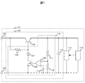
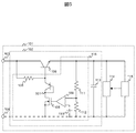
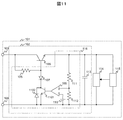
- FIG. 1 shows the configuration of a sensor device according to the first embodiment.
- FIG. 8 shows a configuration of a conventional sensor device.
- FIG. 9 shows a schematic structure of the NPN transistor 106.
- the sensor device 101 in this embodiment includes a power supply terminal 103 that supplies an input voltage Vi, a ground terminal 104, a sensor element 115 that generates an electrical signal corresponding to a physical quantity, and a signal processing circuit 114 that processes an output signal from the sensor element 115. And a regulator 102 that generates a supply voltage Vo from the power supply voltage Vi to the sensor element 115 and the signal processing circuit 114 (hereinafter, the sensor element 115 and the signal processing circuit 114 are collectively referred to as a load circuit).
- the regulator 102 includes an NPN transistor 106 that drives a load circuit, an error detection circuit 116 that controls a base current, and a decoupling capacitor 113.
- the error detection circuit 116 includes resistors 111 and 112 that divide the output voltage Vo of the regulator 102, a reference voltage source 110, an error amplifier 109, an N-type field effect transistor (hereinafter referred to as NMOS) 108 that controls a base current, and a base.
- NMOS N-type field effect transistor
- a resistor 105 for supplying current and a backflow prevention diode 107 are provided. Note that the anode of the backflow prevention diode 107 is connected to the base of the NPN transistor 106 so as to prevent backflow current flowing from the ground into the base of the NPN transistor 106 via the parasitic diode of the NMOS 108.
- the operation of the sensor device in this embodiment will be described with reference to FIGS.
- a stable output voltage Vo is supplied to the load circuit by feedback control of the error detection circuit 116. Since the DC current amplification factor hFE of a bipolar transistor is generally several tens to several hundreds, the current flowing through the base of the NPN transistor 106 is one-hundredth to one-hundredth of the current consumed by the load circuit. Good. When the consumption current of the load circuit decreases, the base current is released to the ground terminal 104 via the NMOS 108.
- the current flowing through the backflow prevention diode 107 is only a few tenths to a few hundredths of the consumption current of the load circuit. Therefore, as described in Japanese Patent Application Laid-Open No. 2007-156641, the current capacity of the diode 107 is about 1 to 2 digits less than that in the case where a diode is inserted between the power supply terminal 103 and the collector of the NPN transistor 106. Good. As a result, the area of the diode 107 can be reduced.
- 2007-156641 is obtained by subtracting a forward voltage drop of about 0.6 V from the diode and a base-emitter voltage drop of about 0.6 V from the NPN transistor from the input voltage Vi. Vi-1.2V.
- the maximum output voltage of the regulator of this embodiment is Vi-0.6V obtained by subtracting about 0.6V between the base and emitter of the NPN transistor 106 from Vi, and a wider range of voltages can be output.
- the effect of the sensor device in this embodiment will be described.
- the first effect is that when a negative surge is input, the charge accumulated in the decoupling capacitor 113 is prevented from flowing out from the emitter terminal 901 of the NPN transistor 106 toward the collector terminal 903, and the load is extended for a longer time. A stable voltage can be supplied to the circuit.
- the second effect is that a wide output voltage range of the normal regulator can be secured by adding the backflow prevention diode 107 to the base terminal 902 instead of the collector terminal 903 of the NPN transistor 106. In other words, a regulator that can operate a load circuit with a lower input voltage is provided.
- the third effect is that the backflow prevention diode 107 is added to the base terminal 902 instead of the collector terminal 903 of the NPN transistor 106, thereby reducing the current capacity required for the backflow prevention diode 107 and reducing the element area. This is a possible point.
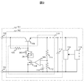
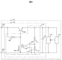
- FIG. 2 shows the configuration of the sensor device according to the second embodiment.
- the sensor device 101 in this embodiment includes a P-type field effect transistor (hereinafter referred to as PMOS) 201 having a well and a gate connected to the drain side, instead of the backflow prevention diode 107 in the sensor device 101 according to the first embodiment. It is characterized by that.
- the base terminal 202 can be connected to the base terminal 202 at a lower resistance by connecting the parasitic diode 202 of the PMOS 201 and the PMOS 201 in the ON state in parallel during normal operation.
- the NMOS 108 can be connected, and the response of the regulator 102 can be further improved.
- the PMOS 201 When a negative surge is applied to the power supply terminal 103, the PMOS 201 is turned off.
- the parasitic diode 202 of the PMOS 201 functions as a backflow prevention diode, so that the backflow current is completely blocked.
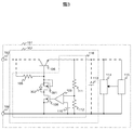
- FIG. 3 shows the configuration of the sensor device according to the third embodiment.
- the sensor device 101 according to the present embodiment is characterized in that an NMOS 301 having a well and a gate connected to the drain side is provided instead of the backflow prevention diode 107 in the sensor device 101 according to the first embodiment.
- the parasitic diode 302 of the NMOS 301 and the NMOS 301 in the ON state are normally connected in parallel, so that the base and the NMOS 108 have a lower resistance. And the response of the regulator 102 can be further improved.
- the NMOS 301 When a negative surge is applied to the power supply terminal 103, the NMOS 301 is turned off. On the other hand, the parasitic diode 302 of the NMOS 301 functions as a backflow prevention diode, so that the backflow current is completely blocked.
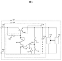
- FIG. 4 shows the configuration of the sensor device according to the fourth embodiment.
- the sensor device 101 according to the present embodiment is characterized in that an NPN transistor 401 having a base connected to the collector side is provided instead of the backflow prevention diode 107 in the sensor device 101 according to the first embodiment.
- the NPN transistor 401 is normally in an ON state and the base and the NMOS 108 can be connected to a low resistance, and the responsiveness of the regulator 102 is further improved. It can be improved.
- the NPN transistor 401 is turned off.
- the diode between the base and the emitter of the NPN transistor 401 functions as a backflow prevention diode, so that the backflow current is completely blocked. .
- FIG. 5 shows the configuration of the sensor device according to the fifth embodiment.
- the sensor device 101 in this embodiment includes a PNP bipolar transistor (hereinafter referred to as a PNP transistor) 501 having a base connected to the collector side, instead of the backflow prevention diode 107 in the sensor device 101 according to the first embodiment. It is characterized by.
- the PNP transistor 501 is normally in an ON state, and the base and the NMOS 108 can be connected with low resistance, and the responsiveness of the regulator 102 is further improved. It can be improved.
- the PNP transistor 501 When a negative surge is applied to the power supply terminal 103, the PNP transistor 501 is turned off. On the other hand, the base-emitter diode of the PNP transistor 501 functions as a backflow prevention diode, so that backflow current is completely blocked. .
- FIG. 6 shows the configuration of the sensor device according to the sixth embodiment.
- the sensor device 101 according to the present embodiment is characterized in that a series resistance element 601 is added to the well of the NMOS 108 instead of the backflow prevention diode 107 in the sensor device 101 according to the first embodiment.
- the backflow current flowing into the base when a negative surge is applied is limited by the resistance element 601, so that the amount of charge flowing from the emitter to the collector can be suppressed without adding an active element, thereby preventing a decrease in output voltage. it can.
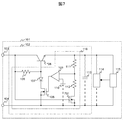
- FIG. 7 shows a configuration of a sensor device according to the seventh embodiment.
- an NMOS 701 is added to the ground terminal side of the voltage dividing resistor 112 of the sensor device 101 according to the first embodiment.
- the gate terminal of the NMOS is connected to the power supply terminal 103.
- the NMOS 701 is in an ON state.
- the gate potential of the NMOS 701 becomes negative, so that the NMOS 701 is turned off and the current flowing through the voltage dividing resistors 111 and 112 can be stopped.
- the current flowing through the voltage dividing resistors 111 and 112 is also reduced, so that the output voltage Vo can be stably maintained for a longer time. .
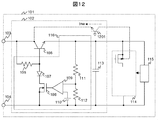
- FIG. 12 is a diagram for explaining the parasitic bipolar transistor 1201, and FIG. 13 shows a cross section of the sensor device according to the eighth embodiment.
- the sensor device 101 according to the present embodiment is obtained by adding a separation region 1303 to the sensor device 101 according to the first embodiment.
- the parasitic bipolar transistor 1201 is a parasitic N-type well 1302 included in the signal processing circuit 114, an N-type well 1301 of the NPN transistor 106 in the regulator 102, and a P substrate or a P-well existing therebetween. It is an NPN transistor.
- an isolation region 1303 is provided between the N-type well 1301 of the NPN transistor 106 and the PMOS N-type well 1302 in the signal processing circuit 114. At this time, the relationship between the length W of the isolation region 1303 and the current amplification factor ⁇ of the parasitic NPN transistor 1201 is expressed by the following equation.
- ⁇ is the minority carrier injection efficiency at the emitter junction
- ⁇ * is the DC current amplification factor of the grounded emitter
- ⁇ B and ⁇ E are the base
- L N and L P are the emitter and base, respectively. Is the diffusion length of minority carriers.
- the current amplification factor ⁇ be at least 0.5 or less.
- FIG. 14 shows an example of the relationship between the length W of the separation region 1303 calculated from the above equation and the current amplification factor ⁇ .
- the relationship between the length W of the isolation region 1303 and the current amplification factor ⁇ varies depending on the impurity concentration and the mobility of carriers, but in order to reduce the current amplification factor ⁇ to 0.5 or less, the length W of the isolation region 1303 is It is desirable to ensure approximately 100 ⁇ m or more. According to such a configuration, in addition to the same effect as the sensor device 101 shown in the first embodiment, the current flowing out to the power supply terminal via the parasitic bipolar transistor can be reduced, so that the output voltage Vo can be reduced for a longer time. It can be maintained stably.
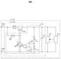
- the technology described so far is not limited to the configuration of the regulator in the first to eighth embodiments.
- the base current of the NPN transistor may be driven by the PMOS 1001 and the NMOS 108.
- the backflow prevention diode 107 when a negative surge is applied, the current flowing from the ground terminal to the base can be blocked by the backflow prevention diode 107, so that the same effect as in the first embodiment can be obtained.
- the backflow prevention diode 107 causes the backflow from the ground terminal 104 via the parasitic diode 1102 of the NPN transistor 1101. Current can be blocked.
- SYMBOLS 101 Sensor apparatus, 102: Regulator, 103: Power supply terminal, 104: Ground terminal, 105: Resistor, 106: NPN bipolar transistor, 107: Backflow prevention diode, 108: N-type field effect transistor, 109: Error amplifier, 110: Reference voltage source, 111: resistor, 112: resistor, 113: decoupling capacitance, 114: signal processing circuit, 115: sensor element, 116: error detection circuit, 201: P-type field effect transistor, 202: parasitic diode, 301: N-type field effect transistor, 302: parasitic diode, 401: NPN bipolar transistor, 501: PNP bipolar transistor, 601: resistor, 701: N-type field effect transistor, 801: parasitic diode, 901: emitter terminal, 902: base terminal, 90 3: collector terminal, 1001: P-type field effect transistor, 1101: NPN bipolar transistor, 1102: parasitic diode,
Landscapes
- Engineering & Computer Science (AREA)
- Physics & Mathematics (AREA)
- General Physics & Mathematics (AREA)
- Electromagnetism (AREA)
- Radar, Positioning & Navigation (AREA)
- Automation & Control Theory (AREA)
- Power Engineering (AREA)
- Semiconductor Integrated Circuits (AREA)
- Continuous-Control Power Sources That Use Transistors (AREA)
- Electronic Switches (AREA)
- Measuring Fluid Pressure (AREA)
Abstract
Description

Claims (11)
- 物理量に応じて電気的特性の変化するセンサ素子と、
前記センサ素子の出力信号を処理する信号処理回路と、
前記センサ素子と前記信号処理回路に電流を供給する第一のトランジスタ素子と、
前記第一のトランジスタ素子のベース電流を制御する制御回路と、
電源端子と、
グラウンド端子と、
を備えるセンサ装置において、
前記制御回路は、前記グラウンド端子から前記第一のトランジスタ素子のベース端子に向かって流れる電流を制限する制限部を備えることを特徴とするセンサ装置。
- 請求項1に記載のセンサ装置において、
前記制御回路は、前記グラウンド端子に向かって電流を流す第二のトランジスタ素子を備え、
前記制限部は、ダイオード素子を備え、前記ダイオード素子は、前記第一のトランジスタ素子のベースとアノードを接続し、前記第二のトランジスタ素子とカソードを接続したことを特徴とするセンサ装置。
- 請求項1に記載のセンサ装置において、
前記制御回路は、前記グラウンド端子に向かって電流を流す第二のトランジスタ素子を備え、
前記制限部は、P型電界効果トランジスタを備え、
前記P型電界効果トランジスタのウェルおよびゲートおよびドレインを前記第二のトランジスタ素子に接続し、前記P型電界効果トランジスタのソースを前記第一のトランジスタ素子のベースに接続したことを特徴とするセンサ装置。
- 請求項1に記載のセンサ装置において、
前記制御回路は、前記グラウンド端子に向かって電流を流す第二のトランジスタ素子を備え、
前記制限部は、N型電界効果トランジスタを備え、
前記N型電界効果トランジスタのソースを前記第二のトランジスタ素子に接続し、
前記N型電界効果トランジスタのウェルおよびゲートおよびドレインを前記第一のトランジスタ素子のベースに接続したことを特徴とするセンサ装置。
- 請求項1に記載のセンサ装置において、
前記制御回路は、前記グラウンド端子に向かって電流を流す第二のトランジスタ素子を備え、
前記制限部は、NPNトランジスタを備え、
前記NPNトランジスタのエミッタを前記第二のトランジスタ素子に接続し、
前記NPNトランジスタのベースおよびコレクタを前記第一のトランジスタ素子のベースに接続したことを特徴とするセンサ装置。
- 請求項1に記載のセンサ装置において、
前記制御回路は、前記グラウンド端子に向かって電流を流す第二のトランジスタ素子を備え、
前記制限部は、PNPトランジスタを備え、
前記PNPトランジスタのベースおよびコレクタを前記第二のトランジスタ素子に接続し、
前記PNPトランジスタのエミッタを前記第一のトランジスタ素子のベースに接続したことを特徴とするセンサ装置
- 請求項1に記載のセンサ装置において、
前記制御回路は、前記グラウンド端子に向かって電流を流す第二のトランジスタ素子を備え、
前記制限部は、前記第二のトランジスタ素子のウェルとグラウンド端子を接続する抵抗素子を備えることを特徴とするセンサ装置。
- 請求項1に記載のセンサ装置において、
前記制御回路は、前記グラウンド端子に向かって電流を流す第二のトランジスタ素子と、分圧用の抵抗素子と、スイッチ部と、を備え、
前記分圧用の抵抗素子の一端と前記グラウンド端子との間に前記スイッチ部が接続され、
前記電源端子に負電圧が印加されたことを検知して前記スイッチ部を切断することを特徴とするセンサ装置。
- 請求項8に記載のセンサ装置において、
前記スイッチ部はN型電界効果トランジスタであることを特徴とするセンサ装置。
- 請求項1乃至9の何れかに記載のセンサ装置において、
前記第一のトランジスタ素子は第一のN型ウェルを備え、
前記信号処理回路は第二のN型ウェルを備え、
前記センサ装置はP型基板またはP型ウェルを備え、
前記第一のN型ウェルと、前記第二のN型ウェルと、前記P型基板または前記P型ウェルと、
で構成される寄生バイポーラトランジスタの電流増幅率αが0.5以下となるように前記第一のN型ウェルと前記第二のN型ウェルとの間に分離領域を設けることを特徴とするセンサ装置。
- 請求項10に記載のセンサ装置において、
前記分離領域の長さが100マイクロメートル以上であることを特徴とするセンサ装置。
Priority Applications (5)
| Application Number | Priority Date | Filing Date | Title |
|---|---|---|---|
| PCT/JP2014/074340 WO2016042593A1 (ja) | 2014-09-16 | 2014-09-16 | センサ装置 |
| JP2016548457A JP6397926B2 (ja) | 2014-09-16 | 2014-09-16 | センサ装置 |
| US15/500,426 US10444031B2 (en) | 2014-09-16 | 2014-09-16 | Sensor device |
| EP14902244.4A EP3196728B1 (en) | 2014-09-16 | 2014-09-16 | Sensor device |
| CN201480081559.XA CN106796437B (zh) | 2014-09-16 | 2014-09-16 | 传感器装置 |
Applications Claiming Priority (1)
| Application Number | Priority Date | Filing Date | Title |
|---|---|---|---|
| PCT/JP2014/074340 WO2016042593A1 (ja) | 2014-09-16 | 2014-09-16 | センサ装置 |
Publications (1)
| Publication Number | Publication Date |
|---|---|
| WO2016042593A1 true WO2016042593A1 (ja) | 2016-03-24 |
Family
ID=55532664
Family Applications (1)
| Application Number | Title | Priority Date | Filing Date |
|---|---|---|---|
| PCT/JP2014/074340 Ceased WO2016042593A1 (ja) | 2014-09-16 | 2014-09-16 | センサ装置 |
Country Status (5)
| Country | Link |
|---|---|
| US (1) | US10444031B2 (ja) |
| EP (1) | EP3196728B1 (ja) |
| JP (1) | JP6397926B2 (ja) |
| CN (1) | CN106796437B (ja) |
| WO (1) | WO2016042593A1 (ja) |
Cited By (1)
| Publication number | Priority date | Publication date | Assignee | Title |
|---|---|---|---|---|
| JP2019087699A (ja) * | 2017-11-10 | 2019-06-06 | ミツミ電機株式会社 | レギュレータ用半導体集積回路 |
Families Citing this family (4)
| Publication number | Priority date | Publication date | Assignee | Title |
|---|---|---|---|---|
| DE102017125129A1 (de) | 2017-10-26 | 2019-05-02 | Endress+Hauser SE+Co. KG | Feldgerät-Elektronik |
| TWI704739B (zh) * | 2019-04-24 | 2020-09-11 | 宏碁股份有限公司 | 電源供應裝置 |
| GB2611826A (en) * | 2021-10-18 | 2023-04-19 | Eaton Intelligent Power Ltd | Solid-state DC device |
| CN113946177B (zh) * | 2021-11-08 | 2025-06-17 | 中煤科工集团上海有限公司 | 一种宽范围电源自适应本安传感器电路 |
Citations (5)
| Publication number | Priority date | Publication date | Assignee | Title |
|---|---|---|---|---|
| JPS57118418U (ja) * | 1981-01-16 | 1982-07-22 | ||
| JP2000312004A (ja) * | 1999-04-27 | 2000-11-07 | Seiko Epson Corp | 低消費電力論理機能回路 |
| JP2001195141A (ja) * | 2000-01-14 | 2001-07-19 | Nec Ic Microcomput Syst Ltd | バンドギャップリファレンス回路 |
| JP2002091582A (ja) * | 2000-09-14 | 2002-03-29 | Denso Corp | 定電圧電源回路 |
| JP2010224825A (ja) * | 2009-03-23 | 2010-10-07 | Toshiba Corp | 半導体集積回路 |
Family Cites Families (21)
| Publication number | Priority date | Publication date | Assignee | Title |
|---|---|---|---|---|
| US3029366A (en) * | 1959-04-22 | 1962-04-10 | Sprague Electric Co | Multiple semiconductor assembly |
| US3665253A (en) | 1970-12-02 | 1972-05-23 | Gte Sylvania Inc | Short circuit protection device for multiple power supplies |
| US4319179A (en) * | 1980-08-25 | 1982-03-09 | Motorola, Inc. | Voltage regulator circuitry having low quiescent current drain and high line voltage withstanding capability |
| JPS58112114A (ja) | 1981-12-25 | 1983-07-04 | Mitsubishi Electric Corp | 直流安定化電源回路 |
| JPS622308A (ja) | 1985-06-27 | 1987-01-08 | Nec Corp | 直流定電圧電源 |
| JPH03131062A (ja) | 1989-10-17 | 1991-06-04 | Seiko Epson Corp | 半導体装置 |
| TW228615B (ja) * | 1992-08-27 | 1994-08-21 | Sanyo Denki Kk | |
| JP2606494Y2 (ja) * | 1993-06-18 | 2000-11-06 | 株式会社コガネイ | 2線式センサ回路 |
| JP3442942B2 (ja) | 1996-10-08 | 2003-09-02 | シャープ株式会社 | 直流安定化電源回路の出力ドライブ回路 |
| JPH11186889A (ja) * | 1997-12-24 | 1999-07-09 | Osram Melco Kk | スイッチ回路及び放電灯点灯装置 |
| JP2000046505A (ja) * | 1998-07-29 | 2000-02-18 | Ckd Corp | 流体圧シリンダ用位置検出装置 |
| JP2000112540A (ja) | 1998-10-09 | 2000-04-21 | Sharp Corp | 直流安定化電源装置 |
| JP2001337729A (ja) | 2000-05-29 | 2001-12-07 | Fujitsu Ten Ltd | シリーズレギュレータ |
| TW517422B (en) * | 2001-05-18 | 2003-01-11 | Palmax Technology Co Ltd | Input protection circuit of hand-held electrical apparatus |
| JP2004327525A (ja) | 2003-04-22 | 2004-11-18 | Matsushita Electric Ind Co Ltd | 半導体集積回路装置 |
| JP2006236223A (ja) * | 2005-02-28 | 2006-09-07 | Aiphone Co Ltd | インターホン回路電源電力供給回路 |
| US7480126B2 (en) * | 2005-04-27 | 2009-01-20 | National Instruments Corporation | Protection and voltage monitoring circuit |
| JP2007156641A (ja) | 2005-12-01 | 2007-06-21 | Nec Electronics Corp | 電源回路 |
| US7518493B2 (en) | 2005-12-01 | 2009-04-14 | Lv Sensors, Inc. | Integrated tire pressure sensor system |
| US9310794B2 (en) * | 2011-10-27 | 2016-04-12 | Rosemount Inc. | Power supply for industrial process field device |
| WO2015015488A1 (en) * | 2013-07-29 | 2015-02-05 | Microsemi Corp. - Analog Mixed Signal Group, Ltd. | Integrated limiter and active filter |
-
2014
- 2014-09-16 WO PCT/JP2014/074340 patent/WO2016042593A1/ja not_active Ceased
- 2014-09-16 EP EP14902244.4A patent/EP3196728B1/en active Active
- 2014-09-16 JP JP2016548457A patent/JP6397926B2/ja active Active
- 2014-09-16 CN CN201480081559.XA patent/CN106796437B/zh active Active
- 2014-09-16 US US15/500,426 patent/US10444031B2/en active Active
Patent Citations (5)
| Publication number | Priority date | Publication date | Assignee | Title |
|---|---|---|---|---|
| JPS57118418U (ja) * | 1981-01-16 | 1982-07-22 | ||
| JP2000312004A (ja) * | 1999-04-27 | 2000-11-07 | Seiko Epson Corp | 低消費電力論理機能回路 |
| JP2001195141A (ja) * | 2000-01-14 | 2001-07-19 | Nec Ic Microcomput Syst Ltd | バンドギャップリファレンス回路 |
| JP2002091582A (ja) * | 2000-09-14 | 2002-03-29 | Denso Corp | 定電圧電源回路 |
| JP2010224825A (ja) * | 2009-03-23 | 2010-10-07 | Toshiba Corp | 半導体集積回路 |
Non-Patent Citations (1)
| Title |
|---|
| See also references of EP3196728A4 * |
Cited By (2)
| Publication number | Priority date | Publication date | Assignee | Title |
|---|---|---|---|---|
| JP2019087699A (ja) * | 2017-11-10 | 2019-06-06 | ミツミ電機株式会社 | レギュレータ用半導体集積回路 |
| JP7007564B2 (ja) | 2017-11-10 | 2022-01-24 | ミツミ電機株式会社 | レギュレータ用半導体集積回路 |
Also Published As
| Publication number | Publication date |
|---|---|
| CN106796437A (zh) | 2017-05-31 |
| EP3196728A4 (en) | 2018-06-20 |
| EP3196728B1 (en) | 2020-12-02 |
| US20170227378A1 (en) | 2017-08-10 |
| US10444031B2 (en) | 2019-10-15 |
| CN106796437B (zh) | 2018-09-11 |
| JP6397926B2 (ja) | 2018-09-26 |
| EP3196728A1 (en) | 2017-07-26 |
| JPWO2016042593A1 (ja) | 2017-04-27 |
Similar Documents
| Publication | Publication Date | Title |
|---|---|---|
| KR102595984B1 (ko) | 볼티지 레귤레이터 | |
| US20080217650A1 (en) | Semiconductor circuit including electrostatic discharge circuit having protection element and trigger transistor | |
| JP6397926B2 (ja) | センサ装置 | |
| JP2007166685A (ja) | 逆流防止回路 | |
| US7626799B2 (en) | Microelectronic device equipped with a thermal protection circuit and thermal protection method for a microelectronic device | |
| US8174808B2 (en) | Load driving device | |
| US8547080B2 (en) | Voltage regulator | |
| US20150256166A1 (en) | Voltage selection circuit and semiconductor integrated circuit device having the same | |
| US9748946B2 (en) | Power supply switching circuit and semiconductor device | |
| US7646246B2 (en) | Semiconductor device | |
| US8164364B2 (en) | Circuitry and method for preventing base-emitter junction reverse bias in comparator differential input transistor pair | |
| US7456441B2 (en) | Single well excess current dissipation circuit | |
| JP5618963B2 (ja) | 半導体装置 | |
| US8917121B2 (en) | Output stage circuit | |
| US20060214234A1 (en) | Semiconductor integrated circuit | |
| CN104851882B (zh) | 半导体集成电路、包括该电路的开关电源以及包括该电源的控制系统 | |
| JP2024155475A (ja) | 半導体装置 | |
| JPH04306715A (ja) | 安定化電源回路 | |
| US6768145B1 (en) | Semiconductor integrated circuit device | |
| JP2016134868A (ja) | パルス信号の伝達回路 |
Legal Events
| Date | Code | Title | Description |
|---|---|---|---|
| 121 | Ep: the epo has been informed by wipo that ep was designated in this application |
Ref document number: 14902244 Country of ref document: EP Kind code of ref document: A1 |
|
| ENP | Entry into the national phase |
Ref document number: 2016548457 Country of ref document: JP Kind code of ref document: A |
|
| REEP | Request for entry into the european phase |
Ref document number: 2014902244 Country of ref document: EP |
|
| WWE | Wipo information: entry into national phase |
Ref document number: 2014902244 Country of ref document: EP |
|
| NENP | Non-entry into the national phase |
Ref country code: DE |