WO2016042884A1 - チップ型セラミック半導体電子部品 - Google Patents
チップ型セラミック半導体電子部品 Download PDFInfo
- Publication number
- WO2016042884A1 WO2016042884A1 PCT/JP2015/069233 JP2015069233W WO2016042884A1 WO 2016042884 A1 WO2016042884 A1 WO 2016042884A1 JP 2015069233 W JP2015069233 W JP 2015069233W WO 2016042884 A1 WO2016042884 A1 WO 2016042884A1
- Authority
- WO
- WIPO (PCT)
- Prior art keywords
- external electrode
- chip
- electronic component
- semiconductor electronic
- layer
- Prior art date
- Legal status (The legal status is an assumption and is not a legal conclusion. Google has not performed a legal analysis and makes no representation as to the accuracy of the status listed.)
- Ceased
Links
Images


Classifications
-
- H—ELECTRICITY
- H01—ELECTRIC ELEMENTS
- H01G—CAPACITORS; CAPACITORS, RECTIFIERS, DETECTORS, SWITCHING DEVICES, LIGHT-SENSITIVE OR TEMPERATURE-SENSITIVE DEVICES OF THE ELECTROLYTIC TYPE
- H01G4/00—Fixed capacitors; Processes of their manufacture
- H01G4/002—Details
- H01G4/228—Terminals
- H01G4/232—Terminals electrically connecting two or more layers of a stacked or rolled capacitor
- H01G4/2325—Terminals electrically connecting two or more layers of a stacked or rolled capacitor characterised by the material of the terminals
-
- H—ELECTRICITY
- H01—ELECTRIC ELEMENTS
- H01C—RESISTORS
- H01C1/00—Details
- H01C1/14—Terminals or tapping points specially adapted for resistors; Arrangements of terminals or tapping points on resistors
- H01C1/1406—Terminals or electrodes formed on resistive elements having positive temperature coefficient
-
- H—ELECTRICITY
- H01—ELECTRIC ELEMENTS
- H01C—RESISTORS
- H01C1/00—Details
- H01C1/14—Terminals or tapping points specially adapted for resistors; Arrangements of terminals or tapping points on resistors
- H01C1/1413—Terminals or electrodes formed on resistive elements having negative temperature coefficient
-
- H—ELECTRICITY
- H01—ELECTRIC ELEMENTS
- H01C—RESISTORS
- H01C1/00—Details
- H01C1/14—Terminals or tapping points specially adapted for resistors; Arrangements of terminals or tapping points on resistors
- H01C1/142—Terminals or tapping points specially adapted for resistors; Arrangements of terminals or tapping points on resistors the terminals or tapping points being coated on the resistive element
Definitions
- the present invention relates to a chip type ceramic semiconductor electronic component such as a thermistor, a varistor, and a capacitor including a positive characteristic (or positive temperature coefficient, PTC) thermistor and a negative characteristic (or negative temperature coefficient, NTC) thermistor.
- a chip type ceramic semiconductor electronic component such as a thermistor, a varistor, and a capacitor including a positive characteristic (or positive temperature coefficient, PTC) thermistor and a negative characteristic (or negative temperature coefficient, NTC) thermistor.
- Patent Document 1 discloses a ceramic body made of semiconductor ceramics, a first external electrode formed on both end faces of the ceramic body, a surface of the first external electrode, and a part of a side surface of the ceramic body.
- the corner portion constituted by the side surface and the end surface of the ceramic body has a curved surface.
- the radius of curvature R of the corner portion of the ceramic body, the maximum thickness y from the end face of the ceramic body of the layer of the first external electrode layer in contact with the ceramic body, and the second external Chip type semiconductors with small variations in individual resistance values by setting the minimum thickness x from the apex of the corner of the ceramic body of the layer in contact with the side surface of the ceramic body among the electrodes within a specific numerical range. It is described that ceramic electronic components can be obtained.
- An object of the present invention is to provide a chip-type ceramic semiconductor electronic component having a small variation in the rate of change in resistance value before and after mounting.
- the inventors have found that when forming the second external electrode, a part of the metal element contained in the first external electrode can be oxidized by heat treatment at a high temperature such as baking. And a part of the metal element contained in the first external electrode tends to diffuse and segregate inside the first external electrode. Furthermore, it has been discovered that the occurrence of such oxidation and / or segregation tends to increase the variation in the rate of change in resistance value before and after mounting in a chip-type ceramic semiconductor electronic component. Based on these findings, the present inventors formed the second external electrode using a resin material that can be cured at a temperature lower than the temperature during the heat treatment such as baking described above, thereby forming the first external electrode. It has been found that oxidation and / or segregation of contained metal elements can be suppressed, and as a result, variation in the rate of change in resistance value before and after mounting in a chip-type ceramic semiconductor electronic component can be reduced. It came to complete.
- a ceramic body including a ceramic semiconductor; A pair of first external electrodes formed on both end faces of the ceramic body; A chip-type ceramic semiconductor electronic component that includes a pair of second external electrodes that cover the first external electrode and extend to a part of the side surface of the ceramic body,
- the second external electrode includes a conductive agent and a thermosetting resin cured at a temperature of 500 ° C. or lower.
- the present invention can obtain a chip-type ceramic semiconductor electronic component having a small variation in the resistance change rate before and after mounting by having the above configuration.
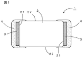
- FIG. 1 is a schematic cross-sectional view of a chip-type ceramic semiconductor electronic component according to the first embodiment of the present invention.
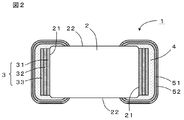
- FIG. 2 is a schematic cross-sectional view of a modification of the chip-type ceramic semiconductor electronic component according to the first embodiment of the present invention.
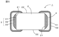
- FIG. 3 is a schematic cross-sectional view of a chip-type ceramic semiconductor electronic component according to the second embodiment of the present invention.
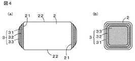
- FIG. 4A is a schematic cross-sectional view of a ceramic body in which first external electrodes are formed on both end surfaces according to an example of a method for manufacturing a chip-type ceramic semiconductor electronic component according to the first embodiment of the present invention.
- FIG. 4B is a side view as seen from the end face side of the ceramic body in which the first external electrodes are formed on both end faces.
- FIG. 5 is a schematic cross-sectional view of a chip-type ceramic semiconductor electronic component manufactured by an example of a method for manufacturing a chip-type ceramic semiconductor electronic component according to the first embodiment of the present invention.
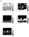
- 6 shows an SEM image of the cross section of the first external electrode and the element mapping result in the chip-type ceramic semiconductor electronic component of Example 1.
- FIG. 7 shows an SEM image and element mapping results of a cross section of the first external electrode in the chip-type ceramic semiconductor electronic component of Comparative Example 1.
- FIG. 1 is a schematic cross-sectional view of the chip-type ceramic semiconductor electronic component according to the first embodiment.
- a chip-type ceramic semiconductor electronic component 1 shown in FIG. 1 includes a ceramic body 2 including a ceramic semiconductor, A pair of first external electrodes 3 formed on both end faces 21 of the ceramic body 2; A pair of second external electrodes 4 that cover the first external electrode 3 and that extend to part of the side surface 22 of the ceramic body 2.
- the ceramic body 2 includes an N-type semiconductor having a positive resistance temperature characteristic as a main component.
- an N-type semiconductor for example, ((Ba, Pb, Sr, Ca) 0.0096 Er 0.004 ) TiO 3 can be used.
- the ceramic body 2 preferably contains about 99.5 to 99.9% by weight of an N-type semiconductor.
- the ceramic body 2 may further contain SiO 2 or MnO 2 in addition to the N-type semiconductor.
- the composition of the ceramic body 2 can be measured by, for example, ICP (inductively coupled plasma) emission spectroscopy or XRF (fluorescence X-ray analysis).
- a pair of first external electrodes 3 are formed on both end faces 21 of the ceramic body 2.
- end faces 21 two surfaces perpendicular to the longitudinal direction of the ceramic body 2
- side faces 21 four faces perpendicular to both end faces 21 are called “side faces” 22.
- the first external electrode 3 may be formed on the entire end face 21 of the ceramic body 2 or may be formed on a part of the end face 21. In the present embodiment, the first external electrode 3 has an ohmic property with respect to the ceramic body 2. Details of the first external electrode 3 will be described later.
- the pair of second external electrodes 4 are formed so as to cover the first external electrode 3 and extend to a part of the side surface 22 of the ceramic body 2.
- the second external electrode 4 covers the entire periphery of the first external electrode 3 and the side surface of the ceramic body 2. 22 is formed so as to extend in part.
- the first external electrode 3 is formed on a part of the end surface 21 of the ceramic body 2
- the second external electrode 4 includes the entire periphery of the first external electrode 3 and the first external electrode 3. It is formed so as to cover the end surface 21 of the ceramic body 2 that is not formed and to extend to a part of the side surface 22 of the ceramic body 2.
- the second external electrode 4 is formed so as to cover the entire end of the ceramic body 2 on which the first external electrode 3 is formed.
- the second external electrode 4 is provided in order to improve solderability at the time of mounting and to prevent oxidation of a metal element contained in the first external electrode. Since the second external electrode 4 is formed so as to extend to a part of the side surface 22 of the ceramic body 2, the substrate and the chip-type ceramic are mounted when the chip-type ceramic semiconductor electronic component 1 is mounted on the substrate. Connectivity with the semiconductor electronic component 1 can be ensured.
- the second external electrode 4 includes a conductive agent and a thermosetting resin cured at a temperature of 500 ° C. or lower.
- the second external electrode 4 can be formed at a temperature lower than that of a conventional heat treatment such as baking.
- a conventional heat treatment such as baking
- the mechanism capable of reducing the variation in the change rate of the resistance value before and after mounting is not limited by any theory, but is as follows. Conceivable.
- the second external electrode 4 can be formed at a relatively low temperature of 500 ° C. or lower by using a thermosetting resin that can be cured at 500 ° C. or lower as the material of the second external electrode 4. .
- a thermosetting resin that can be cured at 500 ° C. or lower as the material of the second external electrode 4.
- formation of the metal oxide in the first external electrode 3 can be suppressed, and the diffusion and segregation of a part of the metal element present in the first external electrode 3, particularly the above-described metal oxide, are suppressed. can do.
- the obtained chip-type ceramic semiconductor electronic component 1 it is considered that variation in the rate of change in resistance value before and after mounting is suppressed.
- a metal oxide is formed in the first external electrode 3, and a part of the metal element present in the first external electrode 3, particularly the above-described metal oxide diffuses to form the first external electrode 3.
- the following is estimated as one of the factors that cause segregation to cause variation in the change rate of the resistance value.
- stress may be applied to the chip-type ceramic semiconductor electronic component 1.
- a part of the metal element present in the first external electrode 3, particularly a metal oxide that may be generated during the formation of the second external electrode 4 is segregated inside the first external electrode 3, the stress described above is applied.
- the stress described above is applied.
- the chip-type ceramic semiconductor electronic component 1 since segregation of the metal element in the first external electrode 3 can be suppressed, even if stress is applied during mounting, generation of cracks is prevented. Can be prevented.
- the chip-type ceramic semiconductor electronic component 1 according to the present embodiment exhibits good deflection strength because the second external electrode 4 includes a thermosetting resin. Therefore, cracks are less likely to occur in the chip-type ceramic semiconductor electronic component 1. Furthermore, the chip-type ceramic semiconductor electronic component 1 according to the present embodiment does not require a second external electrode baking step at a high temperature with high power consumption in the manufacturing process, so that the manufacturing cost can be reduced.
- a metal oxide is formed in the first external electrode 3, and a part of the metal element present in the first external electrode 3, in particular, the above-described metal oxide diffuses to cause the first external electrode to diffuse. Segregation at 3 can result in an increase in resistance at room temperature in the resulting chip-type ceramic semiconductor electronic component 1.
- the chip-type ceramic semiconductor electronic component 1 according to the present embodiment has a chip-type ceramic semiconductor electronic component 1 obtained by suppressing formation of metal oxide, diffusion and segregation of metal elements (particularly metal oxide), An effect of suppressing an increase in resistance value at room temperature can also be brought about. This effect is particularly effective when the chip-type ceramic semiconductor electronic component 1 is a PTC thermistor. By suppressing the increase in the resistance value of the PTC thermistor at room temperature, the difference between the resistance value at room temperature and the resistance value at a temperature higher than the Curie temperature can be increased, and the characteristics of the PTC thermistor can be improved.
- the second external electrode 4 preferably contains a conductive agent and a thermosetting resin cured at a temperature of 250 ° C. or lower.
- the second external electrode 4 can be formed at a much lower temperature of 250 ° C. or lower, so that the oxidation, diffusion and segregation of the metal elements present in the first external electrode 3 can be achieved. Can be more effectively prevented.
- the variation in the change rate of the resistance value before and after mounting can be further reduced.
- thermosetting resin that can be used in the present embodiment is a thermosetting resin that can be cured at a temperature of 500 ° C. or lower, preferably 250 ° C. or lower, and examples thereof include an epoxy resin and a phenol resin. It is not limited. One type of thermosetting resin may be used alone, or two or more types may be mixed and used.
- Examples of the conductive agent that can be used in the present embodiment include, but are not limited to, metal particles containing at least one of Ag, AgPd, Cu, and the like.
- the metal particles used as the conductive agent may be particles made of a single metal or particles made of an alloy containing at least one of the above metal elements. One kind of the above metal particles may be used alone, or two or more kinds may be used in combination.
- the average particle size of the metal particles used as the conductive agent is preferably about 1.0 to 15 ⁇ m.
- the second external electrode 4 preferably contains 10 to 30% by weight of a thermosetting resin and 70 to 90% by weight of a conductive agent.
- the content of the thermosetting resin is 10% by weight or more, the strength of the electrode can be improved.
- the content of the thermosetting resin is 30% by weight or less, sufficient conductivity can be ensured.
- the content of the conductive agent is 70% by weight or more, sufficient conductivity can be ensured.
- the strength of the electrode can be improved.
- the composition of the second external electrode 4 can be measured by, for example, ICP emission spectroscopic analysis or XRF.
- the thickness of the second external electrode from the surface of the first external electrode is preferably 1 to 35 ⁇ m.
- the thickness is 1 to 35 ⁇ m, it is possible to effectively prevent solder explosion that may occur during mounting.
- moisture that may be contained in the electrode may vaporize and blow out from the electrode.
- moisture such as water vapor blows out from the electrode the solder may be blown off and scattered on the substrate. This phenomenon is generally called “solder explosion”.
- the thickness of the second external electrode 4 By setting the thickness of the second external electrode 4 to 35 ⁇ m or less, the absolute amount of moisture that can be contained in the second external electrode 4 can be reduced, and as a result, solder explosion can be effectively prevented. Can do.
- FIG. 2 shows a schematic cross-sectional view of one modified example of the chip-type ceramic semiconductor electronic component 1 according to the present embodiment.
- FIG. 2 shows an embodiment in which the first external electrode 3 has a three-layer structure.
- the first external electrode 3 may be composed of a single layer.
- the chip-type ceramic semiconductor electronic component 1 may further include a first plating layer 51 formed so as to cover the surface of the second external electrode 4.
- the first plating layer 51 is a layer containing at least one of Ni and Cu.
- the first plating layer 51 functions to prevent moisture from blowing out from the inside of the second external electrode 4 during mounting.
- the first plating layer 51 also functions to prevent moisture from entering the chip-type ceramic semiconductor electronic component 1 from the surrounding environment. Further, the first plating layer 51 can prevent the deterioration of the characteristics of the electronic component due to the temperature, humidity, etc. of the surrounding environment, and can improve the heat resistance of the electronic component.
- the thickness of the first plating layer 51 is preferably 3 to 10 ⁇ m. When the thickness is 3 ⁇ m or more, solder explosion can be more effectively prevented. When the thickness is 10 ⁇ m or less, it is possible to suppress the occurrence of cracks in the ceramic body 2 due to thermal contraction of the first plating layer 51 that may occur when the chip-type ceramic semiconductor electronic component 1 is mounted.
- the ratio of the thickness of the second external electrode 4 from the surface of the first external electrode 3 to the thickness of the first plating layer 51 is preferably 5: 1 to 1: 1. Within the above range, it is possible to more effectively prevent solder explosion during mounting.
- the chip-type ceramic semiconductor electronic component 1 may further include a second plating layer 52 formed so as to cover the surface of the first plating layer 51.
- the second plating layer is a layer containing at least Sn.
- the chip-type ceramic semiconductor electronic component 1 includes the second plating layer 52, so that the wettability of the solder during mounting is improved and the mountability is improved.
- the thickness of the second plating layer 52 is preferably 3 to 10 ⁇ m. When the thickness is 3 ⁇ m or more, the wettability of the solder can be stabilized. When the thickness is 10 ⁇ m or less, plating growth on the surface of the ceramic body 2 can be suppressed.
- Plating growth on the surface of the ceramic body 2 may cause a short circuit at the time of mounting, and may cause a poor appearance, a change in ohmic property (resistance value variation), and the like.
- FIG. 2 shows an embodiment including the first plating layer 51 and the second plating layer 52, the second plating layer 52 can be omitted.
- the first external electrode 3 has an ohmic property with respect to the ceramic body 2.
- the first external electrode 3 may be composed of a single layer or may be composed of two or more layers.
- the first external electrode 3 is composed of two or more layers, if at least a layer in contact with the ceramic body 2 among the two or more layers has an ohmic property with respect to the ceramic body 2 Good.
- a layer having ohmic properties with respect to the ceramic body 2 contributes to the resistance characteristics of the chip-type ceramic semiconductor electronic component 1.
- the second external electrode 4 does not substantially contribute to the resistance characteristics.
- the first external electrode 3 is formed of a single layer
- the composition of the first external electrode 3 can be appropriately selected so as to have an ohmic property with respect to the ceramic body 2.
- the first external electrode 3 preferably contains at least one of Cr, Zn—Ag, Ti, W, Zn and V as a main component.
- the first external electrode 3 may be made of at least one of Cr, Zn—Ag, Ti, W, Zn and V, for example.
- the thickness of the first external electrode 3 is preferably 0.07 to 1.0 ⁇ m. When the thickness is 0.07 ⁇ m or more, durability against external force applied during processing such as barrel polishing is improved, and sufficient ohmic properties can be secured.
- the thickness is 1.0.
- the composition of the first external electrode 3 can be measured by, for example, WDX (wavelength dispersive X-ray analysis) or SAM (scanning Auger electron microscope).
- the metal element contained in the first external electrode 3 tends to be oxidized when heat is applied when the second external electrode 4 is formed under a high temperature condition, and the inside of the first external electrode 3 It tends to diffuse and segregate. Segregation can occur particularly at the interface between the first external electrode 3 and the second external electrode 4. When the oxidized metal element diffuses and segregates, a metal oxide layer can be formed at the interface between the first external electrode 3 and the second external electrode 4. In the present invention, since the second external electrode 4 can be formed at a relatively low temperature, such oxidation, diffusion and segregation can be effectively prevented. As a result, it is possible to obtain the chip-type ceramic semiconductor electronic component 1 with a small variation in the change rate of the resistance value before and after mounting.
- the first external electrode 3 includes two or more layers
- the first external electrode 3 includes three layers (31, 32, 33), but the present invention is not limited to this.
- the chip-type ceramic semiconductor electronic component 1 shown in FIG. 2 includes the first plating layer 51 and the second plating layer 52, but the present invention is not limited to this.
- two or more Including the first external electrode 3 including the first layer and the first plating layer 51 and not including the second plating layer 52, including the first external electrode 3 including two or more layers and the first A configuration in which the plating layer 51 and the second plating layer 52 are not included may be employed.
- the first external electrode 3 When the first external electrode 3 includes two or more layers, at least the first layer 31 in contact with the ceramic body 2 among the two or more layers has an ohmic property with respect to the ceramic body 2. It only has to be.
- the composition of the first layer 31 can be appropriately selected so as to have an ohmic property with respect to the ceramic body 2.
- the first layer 31 of the first external electrode 3 preferably contains at least one of Cr, Zn—Ag, Ti, W, Zn, and V.
- the first layer 31 may be made of at least one of Cr, Zn—Ag, Ti, W, Zn, and V, for example.
- the thickness of the first layer 31 is preferably 0.3 to 1.0 ⁇ m. When the thickness is 0.3 ⁇ m or more, durability against external force applied during processing such as barrel polishing is improved, and sufficient ohmic properties can be secured. When the thickness is 1.0 ⁇ m or less, the manufacturing cost can be reduced and the productivity can be improved.
- the first external electrode 3 may further include a second layer 32 formed on the first layer 31.
- the second layer 32 is an adhesive property between the ohmic first layer 31 and the second external electrode 4, or the first layer 31 when the first external electrode 3 includes a third layer 33 described later. This is a layer for improving the adhesion between the first layer 33 and the third layer 33.
- the composition of the second layer 32 can be appropriately set depending on the composition of the first layer 31 and the second external electrode 4 or the third layer 33.
- the second layer 32 is a layer containing Ni and one or more metal elements selected from Cu, Cr and V.
- the second layer 32 preferably contains 50 to 80% by weight of Ni and 20 to 50% by weight of one or more metal elements selected from Cu, Cr and V.
- the thickness of the second layer 32 is preferably 0.5 to 2.0 ⁇ m. When the thickness is 0.5 ⁇ m or more, variation in the rate of change in resistance value can be further suppressed. When the thickness is 2.0 ⁇ m or less, the manufacturing cost can be reduced and the productivity can be improved.
- the metal element contained in the second layer 32 of the first external electrode 3 tends to be oxidized when heat is applied when the second external electrode 4 is formed under a high temperature condition. It tends to diffuse and segregate inside the external electrode 3.
- the first external electrode 3 does not include a third layer 33 to be described later, segregation can occur particularly at the interface between the second layer 32 of the first external electrode 3 and the second external electrode 4.
- a metal oxide layer can be formed at the interface between the second layer 32 and the second external electrode 4.
- segregation may occur particularly at the interface between the second layer 32 and the third layer 33 of the first external electrode 3.
- a metal oxide layer can be formed at the interface between the second layer 32 and the third layer 33.
- the ease of diffusion and segregation of the metal element is the affinity with the metal element contained in the layer in contact with the second layer 32, that is, the second layer 4 of the second external electrode 4 or the third layer 33 of the first external electrode 3. It depends on. For example, when the layer in contact with the second layer 32 (the second external electrode 4 or the third layer 33 of the first external electrode 3) contains Ag as a main component, in the second layer 32, Cu, Cr , V and the like tend to diffuse and segregate.
- the second external electrode 4 can be formed at a relatively low temperature, the above-described oxidation, diffusion and segregation can be effectively prevented. As a result, it is possible to obtain the chip-type ceramic semiconductor electronic component 1 having a small resistance value at room temperature after mounting and a small variation in the change rate of the resistance value.
- the first external electrode 3 may further include a third layer 33 formed on the second layer 32.
- the third layer 33 prevents oxidation of the first layer 31 and the second layer 32, and protects the first layer 31 and the second layer 32 from external force.
- the third layer 33 includes the same conductive agent as the conductive agent included in the second external electrode 4.
- the third layer 33 is a layer including at least one of Ag, AgPd, and Cu.
- the third layer 33 may be made of Ag, for example.
- the thickness of the third layer 33 can be set to 0.5 to 1.5 ⁇ m, for example.
- the chip-type ceramic semiconductor electronic component according to the first embodiment in which the internal electrode is not disposed inside the ceramic body has been described.
- the present invention will be described in the second embodiment below.
- the present invention can be similarly applied to a chip-type ceramic semiconductor electronic component in which an internal electrode is disposed inside a ceramic body.
- the present invention is particularly effective in the chip-type ceramic semiconductor electronic component according to the first embodiment in which the internal electrode is not disposed inside the ceramic body. This is because, in the chip-type ceramic semiconductor electronic component according to the first embodiment, the influence of the oxidation, diffusion, and segregation of the metal element in the first external electrode on the resistance characteristics is large.
- FIG. 3 shows a schematic cross-sectional view of a chip-type ceramic semiconductor electronic component 1 according to the second embodiment of the present invention.
- the chip-type ceramic semiconductor electronic component 1 further includes two or more internal electrodes 6 disposed inside the ceramic body 2.
- the first external electrode 3 is electrically connected to the internal electrode 6.
- the second external electrode 4, the first plating layer 51, and the second plating layer 52 have the same configuration as that of the first embodiment.
- the chip-type ceramic semiconductor electronic component 1 according to the present embodiment may not include the first plating layer 51 and the second plating layer 52.
- the configurations of the ceramic body 2, the first external electrode 3, and the internal electrode 6 can be appropriately set according to desired characteristics.
- the ceramic body 2 may include, for example, (Ba 0.998 Sm 0.002 ) TiO 3 which is a semiconductor ceramic material.
- Sm as a semiconducting agent may be replaced with other rare earth elements such as La and Nd.
- the internal electrode 6 may be a Ni electrode, for example.
- the thickness of the internal electrode 6 is preferably 0.5 to 2.0 ⁇ m. Also in this embodiment, since the second external electrode 4 can be formed at a relatively low temperature, oxidation, diffusion, and segregation of the metal element contained in the first external electrode 3 can be prevented. As a result, it is possible to obtain a chip-type ceramic semiconductor electronic component having a small variation in the change rate of the resistance value before and after mounting.
- the PTC thermistor has been described as an example.
- the present invention is not limited to the PTC thermistor, and can be appropriately applied to other chip-type ceramic semiconductor electronic components such as an NTC thermistor, a varistor, and a capacitor.
- a predetermined amount of ceramic raw materials such as BaCO 3 , TiO 2 , PbO, SrCO 3 , and CaCO 3 and semiconducting agents such as Er 2 O 3 are weighed as raw materials for the ceramic body.
- the semiconducting agent is selected from the group consisting of Y, La, Ce, Pr, Nd, Sm, Eu, Gd, Tb, Dy, Ho, Er, Tm, Yb, and Lu instead of Er 2 O 3
- At least one rare earth element oxide or the like may be used.
- a characteristic improving agent such as Mn 2 O 3 or a sintering aid such as SiO 2 may be used as a raw material for the ceramic body.
- a characteristic improving agent such as Mn 2 O 3 or a sintering aid such as SiO 2
- PSZ ball pulverizing medium
- PSZ partially stabilized zirconia
- the obtained calcined powder is granulated by adding an organic binder, a dispersant and water and mixing with a PSZ ball for a predetermined time.
- An unfired mother substrate is produced by molding the obtained granulated product.
- the unbaked mother substrate is subjected to a binder removal treatment and fired at a predetermined temperature (1200 to 1400 ° C.) in the atmosphere to obtain a mother substrate.
- First external electrodes are formed on both sides of the mother substrate.
- the first external electrode can be formed by a thin film forming method such as sputtering or vapor deposition.
- a mode in which the first external electrode includes three layers will be described, but the present invention is not limited to this mode.
- a Cr layer is formed by sputtering as the first layer of the first external electrode having ohmic properties with respect to the ceramic body.
- a NiCu layer is formed by sputtering as a second layer of the first external electrode.
- an Ag layer is formed as a third layer of the first external electrode by sputtering. In this way, a first external electrode including three layers can be formed.
- the mother substrate on which the first external electrode is formed is cut into a predetermined dimension so as to have the shape of the ceramic body on which the first external electrode is formed.
- the ceramic body on which the first external electrode is formed has, for example, a longitudinal dimension (L dimension) of 0.95 mm, a width dimension (W dimension) of 0.48 mm, and a thickness dimension (T dimension). ) Can be cut to 0.48 mm.
- the longitudinal dimension (L dimension) of the ceramic body on which the first external electrodes are formed includes the thickness of the pair of first external electrodes.
- FIG. 4A illustrates an example of a cross-sectional view of the ceramic body 2 on which the first external electrode 3 is formed after polishing
- FIG. 4 illustrates an example of a side view of the ceramic body 2 viewed from the end face 21 side. Shown in (b).
- each side of the first external electrode 3 may also be curved by polishing. The shape is not limited, and each side of the first external electrode 3 may be linear.
- a conductive paste for forming the second external electrode is prepared.
- a conductive agent such as Ag, AgPd or Cu
- a thermosetting resin such as epoxy resin or phenol resin
- 1 to 5% of a diluent are mixed. It is prepared by.
- the end of the ceramic body on which the first external electrode is formed is immersed in a conductive paste bath and pulled up, and then heat treatment is performed at 500 ° C. or less, preferably about 100 to 250 ° C. In this way, the second external electrode is formed.
- the first plating layer is formed so as to cover the surface of the second external electrode.
- the first plating layer can be formed, for example, by electrolytic plating at least one of Ni and Cu.
- the second plating layer is formed so as to cover the surface of the first plating layer.
- the second plating layer can be formed, for example, by electroplating Sn.
- FIG. 1 An example of the chip-type ceramic semiconductor electronic component 1 obtained by the above manufacturing method is shown in FIG.
- the chip-type ceramic semiconductor electronic component 1 manufactured in this way has an advantage that variation in the rate of change in resistance value is small.
- the manufacturing method of the chip-type ceramic semiconductor electronic component according to the present invention has been described by taking the PTC thermistor having no internal electrode as an example. Ceramic semiconductor electronic components can also be appropriately manufactured based on the description in this specification.
- a PTC thermistor having an internal electrode can be manufactured by the procedure described below.
- Each raw material of the ceramic body is wet-mixed and pulverized, and the resultant mixture is calcined at a predetermined temperature to obtain a calcined powder.
- An organic binder is added to the obtained calcined powder, and a wet mixing process is performed to form a slurry, which is then molded using a doctor blade method or the like to produce a ceramic green sheet.
- the internal electrode conductive paste is applied to the surface of the ceramic green sheet to form an internal electrode pattern.
- the conductive paste for internal electrodes can be prepared, for example, by dispersing Ni metal powder and an organic binder in an organic solvent.
- the internal electrode paste may be applied by screen printing or the like, for example.
- a predetermined number of ceramic green sheets on which internal electrode patterns are formed in this way are stacked, and then the ceramic green sheets on which no internal electrode patterns are formed are sandwiched and pressed together to produce a laminate.
- the laminated body is cut to a predetermined size, then subjected to a binder removal process, and then fired at a predetermined temperature, whereby a ceramic body having internal electrodes is obtained.
- a PTC thermistor having the internal electrodes can be obtained.
- Example 1 The chip-type ceramic semiconductor electronic component of Example 1 was produced by the following procedure.
- the chip-type ceramic semiconductor electronic component of Example 1 is a PTC thermistor.
- a Cr layer having a thickness of 0.3 ⁇ m was formed on both surfaces of the obtained mother substrate by sputtering as a first layer of the first external electrode having ohmic properties with respect to the ceramic body.
- a NiCu layer having a thickness of 1.0 ⁇ m was formed as a second layer of the first external electrode on the first layer of the formed first external electrode by sputtering.
- an Ag layer having a thickness of 1.3 ⁇ m was formed as a third layer of the first external electrode by sputtering.
- the mother substrate on which the first external electrode is formed has a longitudinal dimension (L dimension) of 0.95 mm, a width dimension (W dimension) of 0.48 mm, and a thickness dimension (T).
- the ceramic body on which the first external electrodes were formed was produced by cutting so that the dimension) was 0.48 mm.
- the ceramic body on which the first external electrode thus obtained was formed was polished using cobblestone, polishing powder, etc., so that each side of the ceramic body was curved.
- a conductive paste was prepared by mixing Ag as a conductive agent, an epoxy resin as a thermosetting resin, and a diluent for adjusting viscosity. The end of the ceramic body on which the first external electrode was formed was immersed in this conductive paste bath, pulled up, and then heat treated at 230 ° C. for 30 minutes to form a second external electrode. The thickness of the formed second external electrode from the surface of the first external electrode was 15 ⁇ m.
- Comparative Example 1 The chip-type ceramic semiconductor electronic component of Comparative Example 1 was produced by the following procedure.
- the chip-type ceramic semiconductor electronic component of Comparative Example 1 is a PTC thermistor.
- Example 2 In the same procedure as in Example 1, a mother substrate, a first external electrode, and a ceramic body on which the first external electrode was formed were manufactured.
- a conductive paste for forming the second external electrode was prepared by mixing a conductive agent, glass, a resin component, and an organic solvent. The end of the ceramic body on which the first external electrode was formed was immersed in this conductive paste bath, pulled up, and then baked at 600 ° C. for 30 minutes to form a second external electrode. The thickness of the formed second external electrode from the surface of the first external electrode was 35 ⁇ m.
- a Ni layer was formed as the first plating layer, and then a Sn layer was formed as the second plating layer.
- the chip type ceramic semiconductor electronic component of Comparative Example 1 was obtained by the above procedure.
- FIG. 7 shows the SEM (scanning electron microscope) image of the first external electrode of the ceramic semiconductor electronic component and the result of elemental mapping of O, Cr, Ni and Cu. 6 and 7, the region indicated by (a) is the ceramic body, the region indicated by (b) is the first layer (Cr layer) of the first external electrode, and the region indicated by (c) is the first external electrode. The region indicated by the second layer (NiCu layer) and (d) of the electrode is the third layer (Ag layer) of the first external electrode. From FIG. 6, it can be seen that no segregation of Ni and Cu oxides occurred in the first external electrode of the chip-type ceramic semiconductor electronic component of Example 1.
- FIG. 7 shows that although the oxidation and segregation of Ni did not occur in the first external electrode of the chip-type ceramic semiconductor electronic component of Comparative Example 1, the segregation of Cu oxide occurred. From the result of elemental mapping of the O and Cu elements in FIG. 7, the Cu oxide is segregated at the interface between the second layer (NiCu layer) and the third layer (Ag layer) of the first external electrode. all right. From this result, it can be seen that when the heat treatment (baking) temperature when forming the second external electrode is 600 ° C., the metal element is oxidized and segregated in the first external electrode.
- a current was applied at 15 V to the chip-type ceramic semiconductor electronic component (PTC thermistor) of Example 1 and Comparative Example 1 described above, and the rate of change in resistance value before and after application was measured.
- 100 chip-type ceramic semiconductor electronic components having a resistance value change rate of a certain value or more were prepared for each of Example 1 and Comparative Example 1, and mounted on the substrate by soldering. Mounting was performed under conditions of a top temperature of 260 ° C. and a holding time of 15 seconds. For each PTC thermistor, the resistance value at room temperature (25 ° C.) was measured by a four-terminal method before and after mounting.
- the PTC thermistor of Example 1 has a smaller maximum resistance change rate before and after mounting than the PTC thermistor of Comparative Example 1, and the variation is accordingly reduced. Therefore, by increasing the temperature of the heat treatment when forming the second external electrode to a relatively low temperature of 230 ° C., it is possible to suppress an increase in resistance value during mounting in the PTC thermistor after mounting. It can be said that the variation in the rate of change of the resistance value at the same time could be suppressed.
- the chip-type ceramic semiconductor electronic component according to the present invention is an electronic device in which an increase in resistance value during mounting is suppressed and variation in the resistance value change rate before and after mounting is reduced, and high reliability and high performance are required. It can be applied to equipment.
Landscapes
- Engineering & Computer Science (AREA)
- Microelectronics & Electronic Packaging (AREA)
- Power Engineering (AREA)
- Manufacturing & Machinery (AREA)
- Thermistors And Varistors (AREA)
- Ceramic Capacitors (AREA)
- Fixed Capacitors And Capacitor Manufacturing Machines (AREA)
Abstract
Description
セラミック素体の両端面に形成された1対の第1の外部電極と、
前記第1の外部電極を覆い且つ前記セラミック素体の側面の一部に延在するように形成された1対の第2の外部電極と
を含むチップ型セラミック半導体電子部品であって、
第2の外部電極が、導電剤と、500℃以下の温度で硬化された熱硬化性樹脂とを含む、チップ型セラミック半導体電子部品が提供される。
図1に、第1の実施形態に係るチップ型セラミック半導体電子部品の概略断面図を示す。図1に示すチップ型セラミック半導体電子部品1は、セラミック半導体を含むセラミック素体2と、
セラミック素体2の両端面21に形成された1対の第1の外部電極3と、
第1の外部電極3を覆い且つセラミック素体2の側面22の一部に延在するように形成された1対の第2の外部電極4とを含む。
図3に、本発明の第2の実施形態に係るチップ型セラミック半導体電子部品1の概略断面図を示す。図3に示すように、チップ型セラミック半導体電子部品1は、セラミック素体2の内部に配置された2以上の内部電極6を更に含む。本実施形態において、第1の外部電極3は、内部電極6と電気的に接続している。本実施形態において、第2の外部電極4、第1のめっき層51、第2のめっき層52については、第1の実施形態と同様の構成を有する。なお、本実施形態に係るチップ型セラミック半導体電子部品1は、第1のめっき層51および第2のめっき層52を含まなくてもよい。セラミック素体2、第1の外部電極3および内部電極6の構成については、所望の特性に応じて適宜設定することができる。セラミック素体2は、例えば、半導体セラミック材料である(Ba0.998Sm0.002)TiO3を含んでよい。上記式中、半導体化剤であるSmは、LaやNd等の他の希土類元素で置き換えてもよい。内部電極6は、例えばNi電極であってよい。内部電極6の厚さは0.5~2.0μmであることが好ましい。本実施形態においても、第2の外部電極4が比較的低温で形成することができるので、第1の外部電極3中に含まれる金属元素の酸化、拡散、偏析を防止することができる。その結果、実装前後での抵抗値の変化率のばらつきが小さいチップ型セラミック半導体電子部品を得ることができる。
以下、本発明に係るチップ型セラミック半導体電子部品の製造方法について、上述の第1の実施形態に係るチップ型セラミック半導体電子部品を例として説明するが、製造方法はこれに限定されるものではない。
まず、セラミック素体の原料として、BaCO3、TiO2、PbO、SrCO3、CaCO3等のセラミック原料およびEr2O3等の半導体化剤を所定量秤量する。半導体化剤としては、Er2O3の代わりに、Y、La、Ce、Pr、Nd、Sm、Eu、Gd、Tb、Dy、Ho、Er、Tm、Yb、Luからなる群から選択される少なくとも1つの希土類元素の酸化物などを用いてもよい。また、セラミック素体の原料として、上述のセラミック原料および半導体化剤に加えて、Mn2O3等の特性改善剤や、SiO2等の焼結助剤を用いてもよい。秤量した各原料を、部分安定化ジルコニア(Partially Stabilized Zirconia:PSZ)等の粉砕媒体(以下、PSZボールともよぶ)および純水と共にボールミルに投入し、湿式混合粉砕する。得られた混合物を、所定温度(例えば、1000~1200℃)で仮焼成して、仮焼粉末を得る。得られた仮焼粉末に、有機バインダ、分散剤および水を加え、PSZボールと共に所定時間混合することにより造粒する。得られた造粒物を成形することにより未焼成のマザー基板を作製する。この未焼成のマザー基板に脱バインダ処理を行い、大気中で所定の温度(1200~1400℃)で焼成してマザー基板を得る。
マザー基板の両面に第1の外部電極を形成する。第1の外部電極は、スパッタリング、蒸着等の薄膜形成法により形成することができる。以下、第1の外部電極の形成方法の一例として、第1の外部電極が3つの層を含む形態について説明するが、本発明はこの形態に限定されるものではない。
このようにして第1の外部電極が形成されたマザー基板を、第1の外部電極が形成されたセラミック素体の形状となるように所定の寸法にカットする。第1の外部電極が形成されたセラミック素体は、例えば、長手方向の寸法(L寸)が0.95mm、幅方向の寸法(W寸)が0.48mm、厚さ方向の寸法(T寸)が0.48mmとなるようにカットすることができる。なお、上述の第1の外部電極が形成されたセラミック素体の長手方向の寸法(L寸)は、1対の第1の外部電極の厚さを含んでいる。
まず、第2の外部電極を形成するための導電性ペーストを調製する。導電性ペーストは、Ag、AgPd、Cu等の導電剤70~90重量%と、エポキシ樹脂、フェノール樹脂等の熱硬化性樹脂10~30重量%と、希釈剤1~5%とを混合することにより調製される。第1の外部電極が形成されたセラミック素体の端部を導電性ペースト浴に浸漬し、引き上げた後、500℃以下、好ましくは約100~250℃で熱処理を行う。このようにして第2の外部電極が形成される。
第1のめっき層は、第2の外部電極の表面を覆うように形成される。第1のめっき層は、例えば、NiおよびCuの少なくとも1つを電解めっきすることにより形成することができる。第2のめっき層は、第1のめっき層の表面を覆うように形成される。第2のめっき層は、例えばSnを電解めっきすることにより形成することができる。
実施例1のチップ型セラミック半導体電子部品を下記の手順で作製した。実施例1のチップ型セラミック半導体電子部品は、PTCサーミスタである。
まず、セラミック原料であるBaCO3、PbO、SrCO3、CaCO3およびTiO2、半導体化剤であるEr2O3、ならびに特性改善剤であるMn2O3を所定量秤量した。秤量した各原料を、PSZボールおよび純水と共にボールミルに投入し、湿式混合粉砕した。得られた混合物を1150℃で仮焼成して仮焼粉末を得た。得られた仮焼粉末に、有機バインダであるアクリル酸系バインダ、分散剤および水を加え、PSZボールと共に所定時間混合することにより造粒した。得られた造粒物を成形することにより未焼成のマザー基板を作製した。この未焼成のマザー基板に脱バインダ処理を行い、大気中で最高温度1360℃にて焼成してマザー基板を得た。
得られたマザー基板の両面に、セラミック素体に対してオーミック性を有する第1の外部電極の第1層として、厚さ0.3μmのCr層をスパッタリングにより形成した。形成された第1の外部電極の第1層の上に、第1の外部電極の第2層として、厚さ1.0μmのNiCu層をスパッタリングにより形成した。形成された第1の外部電極の第2層の上に、第1の外部電極の第3層として、厚さ1.3μmのAg層をスパッタリングにより形成した。
このようにして第1の外部電極が形成されたマザー基板を、長手方向の寸法(L寸)が0.95mm、幅方向の寸法(W寸)が0.48mm、厚さ方向の寸法(T寸)が0.48mmとなるようにカットすることにより、第1の外部電極が形成されたセラミック素体を作製した。このようにして得られた第1の外部電極が形成されたセラミック素体を玉石および研磨粉等を用いて研磨することにより、セラミック素体の各辺を曲面状にした。
導電剤であるAg、熱硬化性樹脂であるエポキシ樹脂、および粘度調整用希釈剤を混合することにより導電性ペーストを調製した。第1の外部電極が形成されたセラミック素体の端部をこの導電性ペースト浴に浸漬し、引き上げた後、230℃で30分間熱処理を行うことにより、第2の外部電極を形成した。形成された第2の外部電極の、第1の外部電極の表面からの厚さは15μmであった。
電解めっきにより、第1のめっき層として厚さ6μmのNi層を形成した。次いで、電解めっきにより、第2のめっき層として厚さ4μmのSn層を形成した。以上の手順により、実施例1のチップ型セラミック半導体電子部品が得られた。
比較例1のチップ型セラミック半導体電子部品を下記の手順で作製した。比較例1のチップ型セラミック半導体電子部品は、PTCサーミスタである。
実施例1および比較例1のチップ型セラミック半導体電子部品の第1の外部電極中に存在する元素の分布を調べるために、SAMを用いたオージェ電子分光法により元素マッピングを行った。まず、試料の樹脂固めを行い、試料の厚さ方向に研磨し、厚さ方向の寸法(T寸)の1/2の地点における断面を得た。FIB(集束イオンビーム)を断面に対して5°の角度で照射して加工を行い、オージェ電子分光法による測定を行った。実施例1のチップ型セラミック半導体電子部品の第1の外部電極のSEM(走査型電子顕微鏡)画像ならびにO、Cr、Ni、CuおよびAgの元素マッピングの結果を図6、比較例1のチップ型セラミック半導体電子部品の第1の外部電極のSEM(走査型電子顕微鏡)画像ならびにO、Cr、NiおよびCuの元素マッピングの結果を図7に示す。図6および図7において、(a)で示す領域はセラミック素体、(b)で示す領域は第1の外部電極の第1層(Cr層)、(c)で示す領域は第1の外部電極の第2層(NiCu層)、(d)で示す領域は第1の外部電極の第3層(Ag層)である。図6より、実施例1のチップ型セラミック半導体電子部品の第1の外部電極において、NiおよびCuの酸化物の偏析が起こらなかったことがわかる。この結果より、第2の外部電極を形成するときの熱処理温度が230℃である場合、第1の外部電極における金属元素の酸化物の偏析を防止できたことがわかる。これに対し、図7より、比較例1のチップ型セラミック半導体電子部品の第1の外部電極において、Niの酸化および偏析は起こらなかったが、Cuの酸化物の偏析が起こったことがわかる。図7のOおよびCu元素の元素マッピング結果より、Cuの酸化物は、第1の外部電極の第2層(NiCu層)と第3層(Ag層)との界面において偏析していることがわかった。この結果より、第2の外部電極を形成する時の熱処理(焼き付け)温度が600℃である場合、第1の外部電極における金属元素の酸化および偏析が生じてしまうことがわかる。
上述の実施例1および比較例1のチップ型セラミック半導体電子部品(PTCサーミスタ)に15Vで電流を印加し、印加の前後での抵抗値の変化率を測定した。抵抗値の変化率が一定値以上であったチップ型セラミック半導体電子部品を、実施例1および比較例1のそれぞれについて100個ずつ用意し、はんだ付けにより基板に実装した。実装は、トップ温度260℃、保持時間15秒の条件で行った。それぞれのPTCサーミスタについて、実装の前後に、4端子法により室温(25℃)における抵抗値を測定した。実施例1および比較例1のチップ型セラミック半導体電子部品のそれぞれについて、実装前後での抵抗値の変化率を下記式に基づいて求めた。
(抵抗値の変化率)[%]={(実装後の抵抗値)-(実装前の抵抗値)}/(実装前の抵抗値)×100
実装前後での抵抗値の変化率の平均値、標準偏差および最大値を表1に示す。

2 セラミック素体
21 セラミック素体の端面
22 セラミック素体の側面
3 第1の外部電極
31 第1の外部電極の第1層
32 第1の外部電極の第2層
33 第1の外部電極の第3層
4 第2の外部電極
51 第1のめっき層
52 第2のめっき層
6 内部電極
Claims (9)
- セラミック半導体を含むセラミック素体と、
前記セラミック素体の両端面に形成された1対の第1の外部電極と、
前記第1の外部電極を覆い且つ前記セラミック素体の側面の一部に延在するように形成された1対の第2の外部電極と
を含むチップ型セラミック半導体電子部品であって、
前記第2の外部電極が、導電剤と、500℃以下の温度で硬化された熱硬化性樹脂とを含む、チップ型セラミック半導体電子部品。 - 前記第2の外部電極が、導電剤と、250℃以下の温度で硬化された熱硬化性樹脂とを含む、請求項1に記載のチップ型セラミック半導体電子部品。
- 前記熱硬化性樹脂が、エポキシ樹脂およびフェノール樹脂の少なくとも1つを含む、請求項1または2に記載のチップ型セラミック半導体電子部品。
- 前記導電剤が、Ag、AgPdおよびCuの少なくとも1つを含む金属粒子である、請求項1~3のいずれか1項に記載のチップ型セラミック半導体電子部品。
- 前記第2の外部電極の、前記第1の外部電極の表面からの厚さが、1~35μmである、請求項1~4のいずれか1項に記載のチップ型セラミック半導体電子部品。
- 前記第2の外部電極の表面を覆うように形成された第1のめっき層を更に含み、該第1のめっき層は、NiおよびCuの少なくとも1つを含み、該第1のめっき層の厚さは3~10μmである、請求項1~5のいずれか1項に記載のチップ型セラミック半導体電子部品。
- 前記第2の外部電極の、前記第1の外部電極の表面からの厚さと、前記第1のめっき層の厚さとの比が、5:1~1:1である、請求項6に記載のチップ型セラミック半導体電子部品。
- 前記第1の外部電極が前記セラミック素体に対してオーミック性を有する、請求項1~7のいずれか1項に記載のチップ型セラミック半導体電子部品。
- 前記セラミック素体の内部に配置された2以上の内部電極を更に含み、前記第1の外部電極が前記内部電極と電気的に接続している、請求項1~7のいずれか1項に記載のチップ型セラミック半導体電子部品。
Priority Applications (3)
| Application Number | Priority Date | Filing Date | Title |
|---|---|---|---|
| JP2016548598A JP6394702B2 (ja) | 2014-09-19 | 2015-07-03 | チップ型セラミック半導体電子部品 |
| EP15842099.2A EP3196904B1 (en) | 2014-09-19 | 2015-07-03 | Chip-type ceramic semiconductor electronic component |
| CN201580049926.2A CN107077970A (zh) | 2014-09-19 | 2015-07-03 | 芯片型陶瓷半导体电子部件 |
Applications Claiming Priority (2)
| Application Number | Priority Date | Filing Date | Title |
|---|---|---|---|
| JP2014191452 | 2014-09-19 | ||
| JP2014-191452 | 2014-09-19 |
Publications (1)
| Publication Number | Publication Date |
|---|---|
| WO2016042884A1 true WO2016042884A1 (ja) | 2016-03-24 |
Family
ID=55532929
Family Applications (1)
| Application Number | Title | Priority Date | Filing Date |
|---|---|---|---|
| PCT/JP2015/069233 Ceased WO2016042884A1 (ja) | 2014-09-19 | 2015-07-03 | チップ型セラミック半導体電子部品 |
Country Status (4)
| Country | Link |
|---|---|
| EP (1) | EP3196904B1 (ja) |
| JP (1) | JP6394702B2 (ja) |
| CN (1) | CN107077970A (ja) |
| WO (1) | WO2016042884A1 (ja) |
Cited By (6)
| Publication number | Priority date | Publication date | Assignee | Title |
|---|---|---|---|---|
| TWI656547B (zh) * | 2016-12-14 | 2019-04-11 | 日商村田製作所股份有限公司 | 陶瓷電子零件及其製造方法 |
| JP2021027178A (ja) * | 2019-08-05 | 2021-02-22 | 日立オートモティブシステムズ株式会社 | 電子制御装置 |
| WO2023100538A1 (ja) * | 2021-12-03 | 2023-06-08 | 株式会社村田製作所 | チップ型電子部品 |
| JP2023098301A (ja) * | 2021-12-28 | 2023-07-10 | 株式会社村田製作所 | 電子部品及び電子部品の製造方法 |
| WO2024075457A1 (ja) * | 2022-10-07 | 2024-04-11 | 太陽誘電株式会社 | 積層セラミックコンデンサとその製造方法 |
| US12394544B2 (en) | 2020-09-17 | 2025-08-19 | Murata Manufacturing Co., Ltd. | Chip ceramic semiconductor electronic component |
Families Citing this family (3)
| Publication number | Priority date | Publication date | Assignee | Title |
|---|---|---|---|---|
| KR102483617B1 (ko) * | 2017-12-21 | 2023-01-02 | 삼성전기주식회사 | 적층형 전자 부품 |
| KR102632357B1 (ko) * | 2018-12-21 | 2024-02-02 | 삼성전기주식회사 | 커패시터 부품 |
| KR20240166701A (ko) * | 2023-05-18 | 2024-11-26 | 삼성전기주식회사 | 전자 부품 및 전자 부품 내장기판 |
Citations (8)
| Publication number | Priority date | Publication date | Assignee | Title |
|---|---|---|---|---|
| JPH08162357A (ja) * | 1994-11-30 | 1996-06-21 | Murata Mfg Co Ltd | セラミック電子部品 |
| JPH09115772A (ja) * | 1995-10-19 | 1997-05-02 | Mitsubishi Materials Corp | チップ型電子部品の外部電極 |
| JP2000243662A (ja) * | 1999-02-19 | 2000-09-08 | Tdk Corp | 電子デバイスおよびその製造方法 |
| JP2002015944A (ja) * | 2000-06-30 | 2002-01-18 | Kyocera Corp | セラミックコンデンサ |
| JP2002299154A (ja) * | 2001-04-03 | 2002-10-11 | Hec Japan Technology Kk | 電子部品の製造方法 |
| JP2009206433A (ja) * | 2008-02-29 | 2009-09-10 | Tdk Corp | 積層電子部品およびその製造方法 |
| JP2013191831A (ja) * | 2012-03-13 | 2013-09-26 | Samsung Electro-Mechanics Co Ltd | 積層セラミック電子部品 |
| JP2014022713A (ja) * | 2012-07-18 | 2014-02-03 | Samsung Electro-Mechanics Co Ltd | 積層セラミック電子部品及びその製造方法 |
Family Cites Families (15)
| Publication number | Priority date | Publication date | Assignee | Title |
|---|---|---|---|---|
| JPH04188813A (ja) * | 1990-11-22 | 1992-07-07 | Mitsubishi Materials Corp | 複合セラミックコンデンサ及びその製造方法 |
| JPH0837127A (ja) * | 1994-07-26 | 1996-02-06 | Matsushita Electric Ind Co Ltd | 積層セラミックコンデンサおよびその製造方法 |
| JPH1092606A (ja) * | 1996-09-13 | 1998-04-10 | Mitsubishi Materials Corp | チップ型サーミスタ及びその製造方法 |
| JPH10284343A (ja) * | 1997-04-11 | 1998-10-23 | Mitsubishi Materials Corp | チップ型電子部品 |
| JP2009295602A (ja) * | 2006-08-22 | 2009-12-17 | Murata Mfg Co Ltd | 積層型電子部品、および積層型電子部品の製造方法。 |
| CN101356605B (zh) * | 2006-11-22 | 2012-05-23 | 株式会社村田制作所 | 叠层型电子部件及其制造方法 |
| JP2010123647A (ja) * | 2008-11-18 | 2010-06-03 | Panasonic Corp | セラミックス電子部品、及びこれを用いた電子機器 |
| JP2011003612A (ja) * | 2009-06-16 | 2011-01-06 | Kyocera Chemical Corp | 電子部品およびその製造方法 |
| JP5324390B2 (ja) * | 2009-10-22 | 2013-10-23 | Tdk株式会社 | 積層電子部品 |
| JP5569101B2 (ja) * | 2010-03-31 | 2014-08-13 | 株式会社村田製作所 | 積層正特性サーミスタ及び積層正特性サーミスタの製造方法 |
| JP5569102B2 (ja) * | 2010-03-31 | 2014-08-13 | 株式会社村田製作所 | 積層正特性サーミスタ及び積層正特性サーミスタの製造方法 |
| JP5522533B2 (ja) * | 2010-05-27 | 2014-06-18 | 三菱マテリアル株式会社 | 表面実装型電子部品およびその製造方法 |
| JP5246207B2 (ja) * | 2010-06-04 | 2013-07-24 | 株式会社村田製作所 | チップ型電子部品 |
| JP5835047B2 (ja) * | 2012-03-22 | 2015-12-24 | Tdk株式会社 | セラミック電子部品 |
| JP6070288B2 (ja) * | 2013-03-05 | 2017-02-01 | Tdk株式会社 | セラミック積層電子部品 |
-
2015
- 2015-07-03 JP JP2016548598A patent/JP6394702B2/ja active Active
- 2015-07-03 EP EP15842099.2A patent/EP3196904B1/en active Active
- 2015-07-03 CN CN201580049926.2A patent/CN107077970A/zh active Pending
- 2015-07-03 WO PCT/JP2015/069233 patent/WO2016042884A1/ja not_active Ceased
Patent Citations (8)
| Publication number | Priority date | Publication date | Assignee | Title |
|---|---|---|---|---|
| JPH08162357A (ja) * | 1994-11-30 | 1996-06-21 | Murata Mfg Co Ltd | セラミック電子部品 |
| JPH09115772A (ja) * | 1995-10-19 | 1997-05-02 | Mitsubishi Materials Corp | チップ型電子部品の外部電極 |
| JP2000243662A (ja) * | 1999-02-19 | 2000-09-08 | Tdk Corp | 電子デバイスおよびその製造方法 |
| JP2002015944A (ja) * | 2000-06-30 | 2002-01-18 | Kyocera Corp | セラミックコンデンサ |
| JP2002299154A (ja) * | 2001-04-03 | 2002-10-11 | Hec Japan Technology Kk | 電子部品の製造方法 |
| JP2009206433A (ja) * | 2008-02-29 | 2009-09-10 | Tdk Corp | 積層電子部品およびその製造方法 |
| JP2013191831A (ja) * | 2012-03-13 | 2013-09-26 | Samsung Electro-Mechanics Co Ltd | 積層セラミック電子部品 |
| JP2014022713A (ja) * | 2012-07-18 | 2014-02-03 | Samsung Electro-Mechanics Co Ltd | 積層セラミック電子部品及びその製造方法 |
Non-Patent Citations (1)
| Title |
|---|
| See also references of EP3196904A4 * |
Cited By (8)
| Publication number | Priority date | Publication date | Assignee | Title |
|---|---|---|---|---|
| TWI656547B (zh) * | 2016-12-14 | 2019-04-11 | 日商村田製作所股份有限公司 | 陶瓷電子零件及其製造方法 |
| JP2021027178A (ja) * | 2019-08-05 | 2021-02-22 | 日立オートモティブシステムズ株式会社 | 電子制御装置 |
| US12394544B2 (en) | 2020-09-17 | 2025-08-19 | Murata Manufacturing Co., Ltd. | Chip ceramic semiconductor electronic component |
| WO2023100538A1 (ja) * | 2021-12-03 | 2023-06-08 | 株式会社村田製作所 | チップ型電子部品 |
| JPWO2023100538A1 (ja) * | 2021-12-03 | 2023-06-08 | ||
| JP7687438B2 (ja) | 2021-12-03 | 2025-06-03 | 株式会社村田製作所 | チップ型電子部品 |
| JP2023098301A (ja) * | 2021-12-28 | 2023-07-10 | 株式会社村田製作所 | 電子部品及び電子部品の製造方法 |
| WO2024075457A1 (ja) * | 2022-10-07 | 2024-04-11 | 太陽誘電株式会社 | 積層セラミックコンデンサとその製造方法 |
Also Published As
| Publication number | Publication date |
|---|---|
| JP6394702B2 (ja) | 2018-09-26 |
| EP3196904B1 (en) | 2023-07-26 |
| EP3196904A4 (en) | 2018-05-09 |
| EP3196904A1 (en) | 2017-07-26 |
| CN107077970A (zh) | 2017-08-18 |
| JPWO2016042884A1 (ja) | 2017-06-15 |
Similar Documents
| Publication | Publication Date | Title |
|---|---|---|
| JP6394702B2 (ja) | チップ型セラミック半導体電子部品 | |
| CN101529535B (zh) | 层叠部件 | |
| KR101570459B1 (ko) | 세라믹 전자부품의 제조방법 및 세라믹 전자부품 | |
| JP5064286B2 (ja) | 表面実装型負特性サーミスタ | |
| CN110033922B (zh) | 层叠线圈部件 | |
| KR101761753B1 (ko) | 세라믹 전자부품 | |
| CN102105954B (zh) | 层叠型电子零件 | |
| JP4936087B2 (ja) | 積層正特性サーミスタ | |
| CN104282438A (zh) | 陶瓷电子部件及其制造方法 | |
| WO2012105437A1 (ja) | バリスタ機能付き積層型半導体セラミックコンデンサとその製造方法 | |
| KR100556561B1 (ko) | 적층형 세라믹 전자 부품의 제조방법 | |
| JP7318611B2 (ja) | 積層セラミックコンデンサ | |
| US20150091690A1 (en) | Laminated ptc thermistor element | |
| US11201015B2 (en) | Multilayer type electronic component | |
| CN214099309U (zh) | 线圈部件 | |
| KR102496771B1 (ko) | 적층형 전자부품 | |
| CN115403367B (zh) | 电介质组合物及层叠陶瓷电子部件 | |
| JP7616230B2 (ja) | チップ型セラミック半導体電子部品 | |
| US20230303451A1 (en) | Dielectric composition and multilayer ceramic electronic device | |
| JP2016054225A (ja) | 負特性サーミスタ用半導体セラミック組成物および負特性サーミスタ | |
| JP2016063079A (ja) | 抵抗素子およびその製造方法 | |
| WO2015040881A1 (ja) | セラミックグリーンシート、積層セラミックコンデンサの製造方法、および積層セラミックコンデンサ | |
| JP6739353B2 (ja) | 半導体素子およびその製造方法 | |
| JP6318537B2 (ja) | インダクタの製造方法及びインダクタ | |
| JP6511635B2 (ja) | 積層バリスタの製造方法 |
Legal Events
| Date | Code | Title | Description |
|---|---|---|---|
| 121 | Ep: the epo has been informed by wipo that ep was designated in this application |
Ref document number: 15842099 Country of ref document: EP Kind code of ref document: A1 |
|
| ENP | Entry into the national phase |
Ref document number: 2016548598 Country of ref document: JP Kind code of ref document: A |
|
| REEP | Request for entry into the european phase |
Ref document number: 2015842099 Country of ref document: EP |
|
| WWE | Wipo information: entry into national phase |
Ref document number: 2015842099 Country of ref document: EP |
|
| NENP | Non-entry into the national phase |
Ref country code: DE |