WO2016079983A1 - SiC基板のエッチング方法及び収容容器 - Google Patents
SiC基板のエッチング方法及び収容容器 Download PDFInfo
- Publication number
- WO2016079983A1 WO2016079983A1 PCT/JP2015/005742 JP2015005742W WO2016079983A1 WO 2016079983 A1 WO2016079983 A1 WO 2016079983A1 JP 2015005742 W JP2015005742 W JP 2015005742W WO 2016079983 A1 WO2016079983 A1 WO 2016079983A1
- Authority
- WO
- WIPO (PCT)
- Prior art keywords
- sic substrate
- etching
- tantalum
- silicide layer
- crucible
- Prior art date
- Legal status (The legal status is an assumption and is not a legal conclusion. Google has not performed a legal analysis and makes no representation as to the accuracy of the status listed.)
- Ceased
Links
Images

Classifications
-
- H—ELECTRICITY
- H10—SEMICONDUCTOR DEVICES; ELECTRIC SOLID-STATE DEVICES NOT OTHERWISE PROVIDED FOR
- H10P—GENERIC PROCESSES OR APPARATUS FOR THE MANUFACTURE OR TREATMENT OF DEVICES COVERED BY CLASS H10
- H10P50/00—Etching of wafers, substrates or parts of devices
- H10P50/60—Wet etching
- H10P50/64—Wet etching of semiconductor materials
- H10P50/642—Chemical etching
-
- C—CHEMISTRY; METALLURGY
- C30—CRYSTAL GROWTH
- C30B—SINGLE-CRYSTAL GROWTH; UNIDIRECTIONAL SOLIDIFICATION OF EUTECTIC MATERIAL OR UNIDIRECTIONAL DEMIXING OF EUTECTOID MATERIAL; REFINING BY ZONE-MELTING OF MATERIAL; PRODUCTION OF A HOMOGENEOUS POLYCRYSTALLINE MATERIAL WITH DEFINED STRUCTURE; SINGLE CRYSTALS OR HOMOGENEOUS POLYCRYSTALLINE MATERIAL WITH DEFINED STRUCTURE; AFTER-TREATMENT OF SINGLE CRYSTALS OR A HOMOGENEOUS POLYCRYSTALLINE MATERIAL WITH DEFINED STRUCTURE; APPARATUS THEREFOR
- C30B29/00—Single crystals or homogeneous polycrystalline material with defined structure characterised by the material or by their shape
- C30B29/10—Inorganic compounds or compositions
- C30B29/36—Carbides
-
- C—CHEMISTRY; METALLURGY
- C30—CRYSTAL GROWTH
- C30B—SINGLE-CRYSTAL GROWTH; UNIDIRECTIONAL SOLIDIFICATION OF EUTECTIC MATERIAL OR UNIDIRECTIONAL DEMIXING OF EUTECTOID MATERIAL; REFINING BY ZONE-MELTING OF MATERIAL; PRODUCTION OF A HOMOGENEOUS POLYCRYSTALLINE MATERIAL WITH DEFINED STRUCTURE; SINGLE CRYSTALS OR HOMOGENEOUS POLYCRYSTALLINE MATERIAL WITH DEFINED STRUCTURE; AFTER-TREATMENT OF SINGLE CRYSTALS OR A HOMOGENEOUS POLYCRYSTALLINE MATERIAL WITH DEFINED STRUCTURE; APPARATUS THEREFOR
- C30B33/00—After-treatment of single crystals or homogeneous polycrystalline material with defined structure
- C30B33/08—Etching
- C30B33/12—Etching in gas atmosphere or plasma
-
- C—CHEMISTRY; METALLURGY
- C30—CRYSTAL GROWTH
- C30B—SINGLE-CRYSTAL GROWTH; UNIDIRECTIONAL SOLIDIFICATION OF EUTECTIC MATERIAL OR UNIDIRECTIONAL DEMIXING OF EUTECTOID MATERIAL; REFINING BY ZONE-MELTING OF MATERIAL; PRODUCTION OF A HOMOGENEOUS POLYCRYSTALLINE MATERIAL WITH DEFINED STRUCTURE; SINGLE CRYSTALS OR HOMOGENEOUS POLYCRYSTALLINE MATERIAL WITH DEFINED STRUCTURE; AFTER-TREATMENT OF SINGLE CRYSTALS OR A HOMOGENEOUS POLYCRYSTALLINE MATERIAL WITH DEFINED STRUCTURE; APPARATUS THEREFOR
- C30B35/00—Apparatus not otherwise provided for, specially adapted for the growth, production or after-treatment of single crystals or of a homogeneous polycrystalline material with defined structure
- C30B35/002—Crucibles or containers
-
- H—ELECTRICITY
- H10—SEMICONDUCTOR DEVICES; ELECTRIC SOLID-STATE DEVICES NOT OTHERWISE PROVIDED FOR
- H10P—GENERIC PROCESSES OR APPARATUS FOR THE MANUFACTURE OR TREATMENT OF DEVICES COVERED BY CLASS H10
- H10P50/00—Etching of wafers, substrates or parts of devices
-
- H—ELECTRICITY
- H10—SEMICONDUCTOR DEVICES; ELECTRIC SOLID-STATE DEVICES NOT OTHERWISE PROVIDED FOR
- H10P—GENERIC PROCESSES OR APPARATUS FOR THE MANUFACTURE OR TREATMENT OF DEVICES COVERED BY CLASS H10
- H10P72/00—Handling or holding of wafers, substrates or devices during manufacture or treatment thereof
- H10P72/04—Apparatus for manufacture or treatment
- H10P72/0402—Apparatus for fluid treatment
- H10P72/0418—Apparatus for fluid treatment for etching
Definitions
- the present invention mainly relates to a method of etching a SiC substrate using a container having a tantalum silicide layer provided on the inner space side.
- Patent Documents 1 and 2 disclose this type of technology.
- Patent Document 1 discloses a method of disposing Si pellets (solid Si) in a storage container in order to make the storage container have an Si vapor pressure.
- Patent Document 2 discloses a method of fixing Si to the inner wall surface of the storage container in order to make the storage container have an Si vapor pressure.
- Patent Document 3 proposes a method in which the inner space side of the container is constituted by a tantalum silicide layer, and this tantalum silicide layer is used as a supply source of Si vapor.
- step bunching may occur by heating a SiC substrate, it is known that whether or not this step bunching can be removed depends on the etching rate.
- Si vapor pressure etching to the SiC manufacturing process, a technical problem related to the etching rate of the SiC substrate in the processing step of the SiC substrate used for epitaxial growth and the activation annealing step of the SiC substrate having the ion-implanted epitaxial growth layer explain.
- the SiC substrate can be obtained by cutting an ingot to a predetermined thickness. Since the surface roughness is large when the SiC substrate is cut out from the ingot, it is necessary to flatten the surface by performing processing steps such as mechanical polishing (MP) and chemical mechanical polishing (CMP). However, polishing scratches remaining on the surface of the SiC substrate are substantially removed by performing mechanical polishing, chemical mechanical polishing, etc., but some deep polishing scratches, mechanical polishing, chemical mechanical polishing, etc. An altered layer (hereinafter referred to as latent scratch) having a disordered crystallinity formed by applying pressure to the surface may remain. The polishing scratches and latent scratches may reach a depth of several tens of ⁇ m in some cases, and it is desirable to increase the etching rate in order to efficiently remove such scratches.
- processing steps such as mechanical polishing (MP) and chemical mechanical polishing (CMP).
- polishing scratches remaining on the surface of the SiC substrate are substantially removed by performing mechanical polishing, chemical mechanical polishing, etc., but some deep polishing
- an impurity (hereinafter referred to as dopant) implanted as ions gives a sufficiently high temperature to be substituted (activated) at the SiC crystal lattice position.
- dopant an impurity implanted as ions
- the SiC substrate is etched excessively, a portion having a sufficient dopant concentration is also removed. Therefore, for an SiC substrate having an ion-implanted epitaxial growth layer, it is necessary to accurately control the etching depth at an etching rate at which step bunching does not occur.
- the heating temperature, the pressure of Si, the pressure of an inert gas, and the like are known. However, controlling these parameters may affect other than the etching rate. Therefore, it is preferable that the etching rate can be controlled by various methods.
- the present invention has been made in view of the above circumstances, and its main object is to provide an etching method for controlling the etching rate of a SiC substrate based on the composition of the container.
- the following SiC substrate etching method is provided. That is, in this etching method, the SiC substrate is etched by heating the SiC substrate under the vapor pressure of Si in a state where the SiC substrate is accommodated in the container.
- the container is configured to contain tantalum metal, a tantalum carbide layer is provided on the inner space side of the tantalum metal, and a tantalum silicide layer is further provided on the inner space side of the tantalum carbide layer. . Then, the etching rate of the SiC substrate is controlled based on the difference in the composition of the tantalum silicide layer.
- the etching rate of the SiC substrate can be controlled without changing the heating temperature, Si pressure, or the like.
- the tantalum silicide layer In the etching method of the above SiC substrate, the tantalum silicide layer, TaSi 2, Ta 5 Si 3 , Ta 2 Si, Ta 3 Si, it is preferable to include either of Ta 5 Si 3 C 0.5.
- the etching rate can be controlled using a general compound composed of Ta and Si.
- the SiC substrate etching method it is preferable that at least two storage containers having different compositions of the tantalum silicide layer are used, and the storage containers are selectively used according to the processing to be performed.
- the following is preferable. That is, high-speed etching and low-speed etching can be performed.
- high-speed etching the container having a higher ratio of tantalum to one molecule of a compound constituting the tantalum silicide layer is used.
- low-speed etching the container having the lower ratio of tantalum in one molecule of the compound constituting the tantalum silicide layer is used.
- a container used in the above-described SiC substrate etching method According to a second aspect of the present invention, there is provided a container used in the above-described SiC substrate etching method.
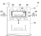
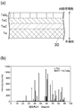
- summary of the high temperature vacuum furnace used for the etching method of this invention The figure which shows the structure of the wall surface of the crucible for low-speed etching, and the X-ray-diffraction pattern of a crucible.
- the high-temperature vacuum furnace 10 includes a main heating chamber 21 and a preheating chamber 22.
- the main heating chamber 21 can heat the SiC substrate 40 (single crystal SiC substrate) having at least a surface made of single crystal SiC to a temperature of 1000 ° C. or higher and 2300 ° C. or lower.
- the preheating chamber 22 is a space for performing preheating before the SiC substrate 40 is heated in the main heating chamber 21.
- a vacuum forming valve 23, an inert gas injection valve 24, and a vacuum gauge 25 are connected to the main heating chamber 21.
- the vacuum forming valve 23 can adjust the degree of vacuum of the main heating chamber 21.
- the inert gas injection valve 24 can adjust the pressure of the inert gas (for example, Ar gas) in the main heating chamber 21.
- the vacuum gauge 25 can measure the degree of vacuum in the main heating chamber 21.
- a heater 26 is provided inside the heating chamber 21.
- a heat reflecting metal plate (not shown) is fixed to the side wall and ceiling of the main heating chamber 21, and the heat reflecting metal plate reflects the heat of the heater 26 toward the center of the main heating chamber 21. It is configured. Thereby, SiC substrate 40 can be heated strongly and evenly, and the temperature can be raised to a temperature of 1000 ° C. or higher and 2300 ° C. or lower.
- the heater 26 for example, a resistance heating type heater or a high frequency induction heating type heater can be used.
- the SiC substrate 40 is heated while being accommodated in the crucible (accommodating container) 30.
- the crucible 30 is placed on an appropriate support base or the like, and is configured to be movable at least from the preheating chamber to the main heating chamber by moving the support base.
- the crucible 30 includes an upper container 31 and a lower container 32 that can be fitted to each other. The detailed configuration of the crucible 30 will be described later.
- the crucible 30 When heat-treating the SiC substrate 40, first, the crucible 30 is placed in the preheating chamber 22 of the high-temperature vacuum furnace 10 as shown by the chain line in FIG. Heat. Next, the crucible 30 is moved to the main heating chamber 21 that has been heated to a preset temperature (for example, about 1800 ° C.) in advance. Thereafter, SiC substrate 40 is heated while adjusting the pressure and the like. Note that preheating may be omitted.
- a preset temperature for example, about 1800 ° C.
- the crucible 30 is configured as shown in FIG. 2 in the portion constituting the wall surface (upper surface, side surface, and bottom surface) of the internal space in which the SiC substrate 40 is accommodated.
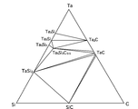
- the crucible 30 is composed of a tantalum layer (Ta), a tantalum carbide layer (TaC and Ta 2 C), and a tantalum silicide layer (TaSi 2 or Ta 5 Si 3 or the like) in order from the outer side to the inner space side.
- Ta tantalum layer
- TaC and Ta 2 C tantalum carbide layer
- TaSi 2 or Ta 5 Si 3 or the like tantalum silicide layer
- This tantalum silicide layer supplies Si to the internal space. Further, since the crucible 30 includes a tantalum layer and a tantalum carbide layer, ambient C vapor can be taken in. Thereby, the inside space can be made into high purity Si atmosphere.
- a crucible composed of a tantalum layer and a tantalum carbide layer is conventionally known.
- a tantalum silicide layer is formed in this crucible.
- Si vaporized in advance at a high temperature is placed in the inner space of the crucible and heated at 1800 ° C. for 15 minutes under a reduced pressure of 10 Pa or less, for example, as shown in FIG.
- a tantalum silicide layer having a composition of 2 is formed.
- FIG. 2B shows an X-ray diffraction pattern of the tantalum silicide layer formed as described above.
- the peak marked with a circle indicates tantalum carbide, and the other peaks indicate TaSi 2 .
- TaSi 2 is sufficiently formed by forming the tantalum silicide layer by the above method.
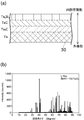
- Ta 5 Si 3 can be formed in addition to TaSi 2 (see FIG. 3A).
- Si vaporized in the same manner as described above is introduced into the internal space of the crucible and heated at 2000 ° C. for 15 minutes under a reduced pressure of 10 Pa or less, for example.
- FIG. 3B shows an X-ray diffraction pattern of the tantalum silicide layer prepared as described above.
- the peak marked with a circle indicates tantalum carbide, and the other peaks indicate Ta 5 Si 3 .
- Ta 5 Si 3 is sufficiently formed by forming the tantalum silicide layer by the above method.
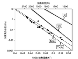
- FIG. 4 shows a graph showing the partial pressure of Si vapor pressure of Si, SiC, TaSi 2 , and Ta 5 Si 3 . It can be seen from FIG. 4 that the Si vapor pressure supplied from TaSi 2 and Ta 5 Si 3 shows a very high pressure. Therefore, it is obvious that the tantalum silicide layer becomes a supply source of Si to the internal space of the crucible 30. Moreover, the tantalum silicide layer is formed over the entire wall surface constituting the internal space. Thereby, the pressure distribution of Si in the internal space can be made uniform. Therefore, SiC substrate 40 can be etched uniformly.
- etching Si vapor pressure etching (hereinafter simply referred to as etching) performed in the present embodiment will be described, and the difference in etching rate when using a crucible 30 having a different composition will be described with reference to FIGS. 5 and 6. explain.
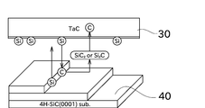
- the SiC substrate 40 is accommodated in the crucible 30 and heated using the high-temperature vacuum furnace 10 in a temperature range of 1500 ° C. to 2200 ° C., preferably 1600 ° C. to 2000 ° C. under high purity Si vapor pressure. Thereby, the surface of SiC substrate 40 is etched. In this etching, the following reaction is performed. Briefly, when the SiC substrate 40 is heated under Si vapor pressure, Si vapor is desorbed from SiC by thermal decomposition. Further, Si vapor is supplied from the tantalum silicide layer. C remaining by the desorption of Si vapor due to thermal decomposition reacts with Si vapor to be sublimated as Si 2 C or SiC 2 .
- the etching rate is considered to be closely related to the rate at which SiC 2 and Si 2 C take in C atoms. Therefore, it is considered that the higher the ratio of the amount of tantalum contained in the compound constituting the tantalum silicide layer, the higher the etching rate. Further, the pressure equilibrium constant of the reaction between SiC 2 and TaSi 2 is smaller than the pressure equilibrium constant of the reaction between SiC 2 and Ta 5 Si 3 . From the above, it is considered that the etching rate when the tantalum silicide layer uses the TaSi 2 crucible 30 is slower than the etching rate when the tantalum silicide layer uses the Ta 5 Si 3 crucible 30.
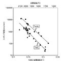
- FIG. 6 shows a case where a 4H—SiC (0001) plane with an off angle of 4 ° is formed in a high vacuum using a crucible 30 having a tantalum silicide layer of TaSi 2 and a crucible 30 having a tantalum silicide layer of Ta 5 Si 3. It is a figure which shows a result when it etches at 1650 to 2100 degreeC under (10 ⁇ -4> Pa). From the graph of FIG. 6, it can be confirmed that the etching rate of the crucible 30 containing TaSi 2 is significantly slower than that of the crucible 30 containing Ta 5 Si 3 .
- the etching rate can be easily changed without changing the heating temperature or the like by properly using the crucibles 30 having different tantalum silicide layer compositions.
- the crucible 30 is properly used.
- FIG. 7 is a view showing a micrograph and surface roughness of the surface of the SiC substrate 40 when etching is performed while changing the pressure (that is, the etching rate) of an inert gas (Ar gas) during etching.
- the pressure of the inert gas is 1.3 kPa
- the surface roughness is high, and it can be seen from the micrograph that step bunching clearly remains.
- the pressure of the inert gas is 133 Pa
- the surface roughness is remarkably reduced, and it can be seen from the micrograph that a part of the step bunching is removed.
- the pressure of the inert gas is 13 Pa and 1.3 Pa and when the vacuum is high, the surface roughness is further reduced, and it can be seen from the micrograph that almost all step bunching can be removed. In this way, whether or not the step bunching is removed can be selected according to the pressure of the inert gas (that is, the etching rate).
- the SiC substrate 40 in which step bunching does not occur has high performance as a semiconductor element because local concentration of the electric field does not occur.
- the SiC substrate 40 in which step bunching has occurred can further eliminate the influence of crystal defects (dislocations) when performing, for example, a solution growth method. Therefore, it is preferable to switch the occurrence of step bunching depending on the situation.
- the etching rate can be switched only by using different crucibles 30. Therefore, when manufacturing the SiC substrate 40 in which step bunching does not occur, the crucible 30 having a tantalum silicide layer of Ta 5 Si 3 is used. Etching (high-speed etching) may be performed. On the other hand, when manufacturing the SiC substrate 40 in which step bunching occurs, etching (low-speed etching) may be performed using the crucible 30 whose tantalum silicide layer is TaSi 2 .
- an ingot composed of a 4H—SiC single crystal or a 6H—SiC single crystal is cut out to a predetermined thickness.
- processing such as mechanical polishing and chemical mechanical polishing is performed in order to remove irregularities formed on the surface of the SiC substrate 40 at the time of cutting. Since the unevenness of the unevenness is considerably large, it is required to polish the SiC substrate 40 at a high speed.
- latent scratch an altered layer with disordered crystallinity
- it is required to polish the SiC substrate 40 at a high speed. Therefore, in order to remove latent scratches instead of mechanical polishing and chemical mechanical polishing, etc., it is possible to perform etching (high-speed etching) more simply than before by using the crucible 30 whose tantalum silicide layer is Ta 5 Si 3. it can.
- the epitaxial layer growth, ion implantation, and impurities implanted as ions are performed on the SiC substrate 40 that has undergone the processing step.
- dopant impurities implanted as ions
- Etching is then performed to remove the dopant deficient portion and planarize the roughened surface by ion implantation.
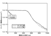
- the dopant deficient portion varies depending on the ion implantation conditions, but exists in a region of about several tens to several hundreds nm from the surface of the SiC substrate 40, for example.
- the dopant concentration is lower in the portion from the surface to several tens of nm and becomes deeper than about 500 nm.
- the dopant concentration is reduced. Therefore, in order to leave a portion having a sufficient dopant concentration while removing the dopant-deficient portion, it is necessary to precisely control the etching amount. Therefore, it is preferable to reduce the etching rate. However, if the etching rate is lower than the predetermined rate as described above, step bunching cannot be removed.
- this etching is precise under the condition that the tantalum silicide layer uses the TaSi 2 crucible 30 and step bunching does not occur in order to prevent excessive removal of the portion where the dopant is sufficiently present. Etching (low-speed etching) may be performed.
- etching can be performed at an appropriate etching rate without much change in the heating temperature or the like.
- the SiC substrate 40 is etched by heating under the vapor pressure of Si while the SiC substrate 40 is accommodated in the crucible 30.
- the crucible 30 includes tantalum metal, and a tantalum carbide layer is provided on the inner space side of the tantalum metal, and a tantalum silicide layer is further provided on the inner space side of the tantalum carbide layer. Then, the etching rate of SiC substrate 40 is controlled based on the difference in the composition of the tantalum silicide layer.
- the etching rate of the SiC substrate 40 can be controlled without changing the heating temperature, the Si pressure, or the like.
- the composition of the tantalum silicide layer is different from each other (specifically, TaSi 2 and Ta 5 Si 3 ), and at least two crucibles 30 are used according to the processing to be performed. Use the crucible 30 properly.
- high-speed etching and low-speed etching can be performed.
- a crucible 30 having a higher ratio of tantalum to one molecule of a compound constituting the tantalum silicide layer (specifically, Ta 5 Si 3 ) is used.
- a crucible 30 is used which has a lower proportion of tantalum (specifically, TaSi 2 ) in one molecule of the compound constituting the tantalum silicide layer.
- TaSi 2 or Ta 5 Si 3 is formed as tantalum silicide.
- tantalum silicide represented by another chemical formula may be formed.
- Ta 2 Si, Ta 3 Si, or Ta 5 Si 3 C 0.5 may be formed. Note that in this specification, even if other atoms such as Ta 5 Si 3 C 0.5 are included, it corresponds to the tantalum silicide layer.
- tantalum silicide having the same composition is formed over the entire inner wall surface of one crucible 30, but tantalum silicide having a plurality of compositions may be formed on the inner wall surface of one crucible 30.
- the etching rate of only a part of the surface of the SiC substrate 40 can be increased or decreased, and the SiC substrate 40 having a desired shape can be generated in consideration thereof.
- the temperature conditions and pressure conditions described above are examples and can be changed as appropriate. Further, a heating device other than the high-temperature vacuum furnace 10 described above may be used, or a container having a shape or material different from that of the crucible 30 may be used.
- the outer shape of the storage container is not limited to a cylindrical shape, and may be a cubic shape or a rectangular parallelepiped shape.
Landscapes
- Chemical & Material Sciences (AREA)
- Engineering & Computer Science (AREA)
- Crystallography & Structural Chemistry (AREA)
- Materials Engineering (AREA)
- Metallurgy (AREA)
- Organic Chemistry (AREA)
- Physics & Mathematics (AREA)
- Plasma & Fusion (AREA)
- Inorganic Chemistry (AREA)
- Crystals, And After-Treatments Of Crystals (AREA)
- Chemical Kinetics & Catalysis (AREA)
- General Chemical & Material Sciences (AREA)
- Drying Of Semiconductors (AREA)
Abstract
Description
(1) SiC(s) → Si(v)I + C(s)
(2) TaxSiy →Si(v)II +Tax’Siy’
(3) 2C(s) + Si(v)I+II → SiC2(v)
(4) C(s) + 2Si(v)I+II → Si2C(v)
30 坩堝(収容容器)
40 SiC基板
Claims (5)
- 収容容器にSiC基板を収容した状態で当該SiC基板をSiの蒸気圧下で加熱することで当該SiC基板をエッチングするエッチング方法において、
前記収容容器は、タンタル金属を含んで構成されるとともに、当該タンタル金属よりも内部空間側にタンタルカーバイド層が設けられ、当該タンタルカーバイド層よりも更に内部空間側にタンタルシリサイド層が設けられており、前記タンタルシリサイド層の組成の違いに基づいて前記SiC基板のエッチング速度が制御されることを特徴とするSiC基板のエッチング方法。 - 請求項1に記載のSiC基板のエッチング方法であって、
前記タンタルシリサイド層は、TaSi2、Ta5Si3、Ta2Si、Ta3Si、Ta5Si3C0.5の何れかを含むことを特徴とするSiC基板のエッチング方法。 - 請求項1に記載のSiC基板のエッチング方法であって、
前記タンタルシリサイド層の組成が互いに異なる少なくとも2つの前記収容容器を用い、実施する処理に応じて前記収容容器を使い分けることを特徴とするSiC基板のエッチング方法。 - 請求項3に記載のSiC基板のエッチング方法であって、
高速エッチングと低速エッチングとを実施可能であり、
高速エッチングを行う場合は、前記タンタルシリサイド層を構成する化合物の1分子に占めるタンタルの割合が高い方の前記収容容器を用い、
低速エッチングを行う場合は、前記タンタルシリサイド層を構成する化合物の1分子に占めるタンタルの割合が低い方の前記収容容器を用いることを特徴とするSiC基板のエッチング方法。 - 請求項1に記載のSiC基板のエッチング方法で用いられることを特徴とする収容容器。
Priority Applications (5)
| Application Number | Priority Date | Filing Date | Title |
|---|---|---|---|
| US15/527,622 US10388536B2 (en) | 2014-11-18 | 2015-11-17 | Etching method for SiC substrate and holding container |
| EP15861337.2A EP3223303B1 (en) | 2014-11-18 | 2015-11-17 | Etching method for sic substrate and use of holding container |
| JP2016560059A JP6751874B2 (ja) | 2014-11-18 | 2015-11-17 | SiC基板のエッチング方法 |
| KR1020177016190A KR20170085085A (ko) | 2014-11-18 | 2015-11-17 | SiC 기판의 에칭 방법 및 수용 용기 |
| CN201580062705.9A CN107004592B (zh) | 2014-11-18 | 2015-11-17 | 碳化硅基板的蚀刻方法及收容容器 |
Applications Claiming Priority (2)
| Application Number | Priority Date | Filing Date | Title |
|---|---|---|---|
| JP2014233631 | 2014-11-18 | ||
| JP2014-233631 | 2014-11-18 |
Publications (1)
| Publication Number | Publication Date |
|---|---|
| WO2016079983A1 true WO2016079983A1 (ja) | 2016-05-26 |
Family
ID=56013556
Family Applications (1)
| Application Number | Title | Priority Date | Filing Date |
|---|---|---|---|
| PCT/JP2015/005742 Ceased WO2016079983A1 (ja) | 2014-11-18 | 2015-11-17 | SiC基板のエッチング方法及び収容容器 |
Country Status (7)
| Country | Link |
|---|---|
| US (1) | US10388536B2 (ja) |
| EP (1) | EP3223303B1 (ja) |
| JP (1) | JP6751874B2 (ja) |
| KR (1) | KR20170085085A (ja) |
| CN (1) | CN107004592B (ja) |
| TW (1) | TWI659463B (ja) |
| WO (1) | WO2016079983A1 (ja) |
Cited By (7)
| Publication number | Priority date | Publication date | Assignee | Title |
|---|---|---|---|---|
| WO2018216657A1 (ja) * | 2017-05-25 | 2018-11-29 | 東洋炭素株式会社 | SiCウエハの製造方法、エピタキシャルウエハの製造方法、及びエピタキシャルウエハ |
| JPWO2020179794A1 (ja) * | 2019-03-05 | 2020-09-10 | ||
| JPWO2020179793A1 (ja) * | 2019-03-05 | 2020-09-10 | ||
| WO2020203516A1 (ja) | 2019-03-29 | 2020-10-08 | 学校法人関西学院 | 温度勾配反転手段を備える半導体基板の製造装置及び半導体基板の製造方法 |
| JPWO2021025077A1 (ja) * | 2019-08-06 | 2021-02-11 | ||
| WO2023189056A1 (ja) * | 2022-03-31 | 2023-10-05 | ローム株式会社 | 炉心管、熱処理装置および支持ユニット |
| WO2025057772A1 (ja) * | 2023-09-15 | 2025-03-20 | 学校法人関西学院 | SiC基板の処理方法、SiC基板の加工変質層を取り除く方法及びSiC基板の表面粗さを低減させる方法 |
Families Citing this family (6)
| Publication number | Priority date | Publication date | Assignee | Title |
|---|---|---|---|---|
| JP7534579B2 (ja) * | 2019-03-05 | 2024-08-15 | 学校法人関西学院 | SiCエピタキシャル基板の製造方法及びその製造装置 |
| EP4012079B1 (en) * | 2019-08-06 | 2025-10-15 | Kwansei Gakuin Educational Foundation | Method for producing a sic substrate |
| CN114342045B (zh) * | 2019-08-06 | 2025-09-19 | 学校法人关西学院 | SiC衬底的制造方法 |
| CN114430781B (zh) * | 2019-08-06 | 2024-04-30 | 学校法人关西学院 | SiC籽晶、SiC晶锭、SiC晶片及它们的制造方法 |
| CN113550012B (zh) * | 2021-07-28 | 2022-11-18 | 浙江大学杭州国际科创中心 | 一种用于碱蒸汽腐蚀碳化硅晶片的装置 |
| CN117080061A (zh) * | 2023-10-16 | 2023-11-17 | 希科半导体科技(苏州)有限公司 | 碳化硅衬底的平整方法、碳化硅衬底以及半导体器件 |
Citations (4)
| Publication number | Priority date | Publication date | Assignee | Title |
|---|---|---|---|---|
| JP2008230944A (ja) * | 2007-03-23 | 2008-10-02 | Kwansei Gakuin | 単結晶炭化ケイ素基板の表面平坦化方法、単結晶炭化ケイ素基板の製造方法、及び単結晶炭化ケイ素基板 |
| JP2010265126A (ja) * | 2009-05-12 | 2010-11-25 | Kwansei Gakuin | 単結晶SiC基板、エピタキシャル成長層付き単結晶SiC基板、SiC基板、炭素供給フィード基板及び炭素ナノ材料付きSiC基板 |
| JP2011233780A (ja) * | 2010-04-28 | 2011-11-17 | Kwansei Gakuin Univ | 半導体素子の製造方法 |
| WO2014076964A1 (ja) * | 2012-11-16 | 2014-05-22 | 東洋炭素株式会社 | 収容容器、収容容器の製造方法、半導体の製造方法、及び半導体製造装置 |
Family Cites Families (10)
| Publication number | Priority date | Publication date | Assignee | Title |
|---|---|---|---|---|
| US6547877B2 (en) * | 1996-01-22 | 2003-04-15 | The Fox Group, Inc. | Tantalum crucible fabrication and treatment |
| TWI600081B (zh) * | 2012-11-16 | 2017-09-21 | 東洋炭素股份有限公司 | Surface treatment method of single crystal silicon carbide substrate and single crystal silicon carbide substrate |
| US20140342553A1 (en) * | 2013-05-14 | 2014-11-20 | United Microelectronics Corp. | Method for Forming Semiconductor Structure Having Opening |
| JP6080075B2 (ja) * | 2013-06-13 | 2017-02-15 | 学校法人関西学院 | SiC基板の表面処理方法 |
| WO2015009495A1 (en) * | 2013-07-17 | 2015-01-22 | Cook Medical Technologies Llc | Ablation mesh |
| JP6247566B2 (ja) * | 2014-02-28 | 2017-12-13 | 東洋炭素株式会社 | 加熱処理容器、加熱処理容器集合体、及び、半導体素子製造装置 |
| JP6232329B2 (ja) * | 2014-03-31 | 2017-11-15 | 東洋炭素株式会社 | SiC種結晶の加工変質層の除去方法、SiC種結晶及びSiC基板の製造方法 |
| JP6330531B2 (ja) * | 2014-07-08 | 2018-05-30 | 株式会社リコー | 画像記録システム及び画像記録方法 |
| CN107002288B (zh) * | 2014-11-18 | 2020-10-16 | 学校法人关西学院 | 碳化硅基板的表面处理方法 |
| US10014176B2 (en) * | 2014-11-18 | 2018-07-03 | Toyo Tanso Co., Ltd. | SiC substrate treatment method |
-
2015
- 2015-11-17 WO PCT/JP2015/005742 patent/WO2016079983A1/ja not_active Ceased
- 2015-11-17 CN CN201580062705.9A patent/CN107004592B/zh active Active
- 2015-11-17 US US15/527,622 patent/US10388536B2/en active Active
- 2015-11-17 KR KR1020177016190A patent/KR20170085085A/ko not_active Abandoned
- 2015-11-17 JP JP2016560059A patent/JP6751874B2/ja active Active
- 2015-11-17 EP EP15861337.2A patent/EP3223303B1/en active Active
- 2015-11-18 TW TW104138126A patent/TWI659463B/zh not_active IP Right Cessation
Patent Citations (4)
| Publication number | Priority date | Publication date | Assignee | Title |
|---|---|---|---|---|
| JP2008230944A (ja) * | 2007-03-23 | 2008-10-02 | Kwansei Gakuin | 単結晶炭化ケイ素基板の表面平坦化方法、単結晶炭化ケイ素基板の製造方法、及び単結晶炭化ケイ素基板 |
| JP2010265126A (ja) * | 2009-05-12 | 2010-11-25 | Kwansei Gakuin | 単結晶SiC基板、エピタキシャル成長層付き単結晶SiC基板、SiC基板、炭素供給フィード基板及び炭素ナノ材料付きSiC基板 |
| JP2011233780A (ja) * | 2010-04-28 | 2011-11-17 | Kwansei Gakuin Univ | 半導体素子の製造方法 |
| WO2014076964A1 (ja) * | 2012-11-16 | 2014-05-22 | 東洋炭素株式会社 | 収容容器、収容容器の製造方法、半導体の製造方法、及び半導体製造装置 |
Non-Patent Citations (1)
| Title |
|---|
| See also references of EP3223303A4 * |
Cited By (20)
| Publication number | Priority date | Publication date | Assignee | Title |
|---|---|---|---|---|
| WO2018216657A1 (ja) * | 2017-05-25 | 2018-11-29 | 東洋炭素株式会社 | SiCウエハの製造方法、エピタキシャルウエハの製造方法、及びエピタキシャルウエハ |
| TWI811529B (zh) * | 2019-03-05 | 2023-08-11 | 學校法人關西學院 | 碳化矽基板、碳化矽基板的製造方法、碳化矽基板的製造裝置以及降低碳化矽基板的宏階褶的方法 |
| JPWO2020179794A1 (ja) * | 2019-03-05 | 2020-09-10 | ||
| JPWO2020179793A1 (ja) * | 2019-03-05 | 2020-09-10 | ||
| WO2020179794A1 (ja) * | 2019-03-05 | 2020-09-10 | 学校法人関西学院 | SiC基板の製造方法及びその製造装置及びSiC基板の加工変質層を低減する方法 |
| WO2020179793A1 (ja) * | 2019-03-05 | 2020-09-10 | 学校法人関西学院 | SiC基板の製造方法及びその製造装置及びSiC基板のマクロステップバンチングを低減する方法 |
| US12451348B2 (en) | 2019-03-05 | 2025-10-21 | Kwansei Gakuin Educational Foundation | Method and device for manufacturing sic substrate, and method for reducing macro-step bunching of sic substrate |
| US11972949B2 (en) | 2019-03-05 | 2024-04-30 | Kwansei Gakuin Educational Foundation | SiC substrate manufacturing method and manufacturing device, and method for reducing work-affected layer in sic substrate |
| JP7464807B2 (ja) | 2019-03-05 | 2024-04-10 | 学校法人関西学院 | SiC基板の製造方法及びその製造装置及びSiC基板のマクロステップバンチングを低減する方法 |
| JP7464808B2 (ja) | 2019-03-05 | 2024-04-10 | 学校法人関西学院 | SiC基板の製造方法及びその製造装置及びSiC基板の加工変質層を低減する方法 |
| WO2020203516A1 (ja) | 2019-03-29 | 2020-10-08 | 学校法人関西学院 | 温度勾配反転手段を備える半導体基板の製造装置及び半導体基板の製造方法 |
| US12014939B2 (en) | 2019-03-29 | 2024-06-18 | Kwansei Gakuin Educational Foundation | Device for manufacturing semiconductor substrate comprising temperature gradient inversion means and method for manufacturing semiconductor substrate |
| JP7541642B2 (ja) | 2019-03-29 | 2024-08-29 | 学校法人関西学院 | 温度勾配反転手段を備える半導体基板の製造装置及び半導体基板の製造方法 |
| JPWO2020203516A1 (ja) * | 2019-03-29 | 2020-10-08 | ||
| JP7274154B2 (ja) | 2019-08-06 | 2023-05-16 | 株式会社デンソー | SiC基板の製造方法 |
| WO2021025077A1 (ja) * | 2019-08-06 | 2021-02-11 | 株式会社デンソー | SiC基板の製造方法 |
| JPWO2021025077A1 (ja) * | 2019-08-06 | 2021-02-11 | ||
| US12237378B2 (en) | 2019-08-06 | 2025-02-25 | Kwansei Gakuin Educational Foundation | Method for manufacturing SiC substrate |
| WO2023189056A1 (ja) * | 2022-03-31 | 2023-10-05 | ローム株式会社 | 炉心管、熱処理装置および支持ユニット |
| WO2025057772A1 (ja) * | 2023-09-15 | 2025-03-20 | 学校法人関西学院 | SiC基板の処理方法、SiC基板の加工変質層を取り除く方法及びSiC基板の表面粗さを低減させる方法 |
Also Published As
| Publication number | Publication date |
|---|---|
| EP3223303A1 (en) | 2017-09-27 |
| CN107004592A (zh) | 2017-08-01 |
| JPWO2016079983A1 (ja) | 2017-10-12 |
| EP3223303B1 (en) | 2023-03-15 |
| TWI659463B (zh) | 2019-05-11 |
| CN107004592B (zh) | 2020-12-08 |
| US10388536B2 (en) | 2019-08-20 |
| TW201630061A (zh) | 2016-08-16 |
| JP6751874B2 (ja) | 2020-09-09 |
| KR20170085085A (ko) | 2017-07-21 |
| EP3223303A4 (en) | 2018-05-30 |
| US20170323797A1 (en) | 2017-11-09 |
Similar Documents
| Publication | Publication Date | Title |
|---|---|---|
| JP6751874B2 (ja) | SiC基板のエッチング方法 | |
| JP5152887B2 (ja) | 単結晶炭化ケイ素基板の表面改質方法、単結晶炭化ケイ素薄膜の形成方法、イオン注入アニール方法及び単結晶炭化ケイ素基板、単結晶炭化ケイ素半導体基板 | |
| US9978597B2 (en) | Method for treating the surface of a silicon-carbide substrate including a removal step in which a modified layer produced by polishing is removed by heating under Si vapor pressure | |
| JP6751875B2 (ja) | SiC基板の表面処理方法 | |
| KR102021644B1 (ko) | 단결정 SiC 기판의 표면 처리 방법 및 단결정 SiC 기판 | |
| TWI671438B (zh) | SiC(碳化矽)種晶之加工變質層的除去方法、SiC種晶及SiC基板之製造方法 | |
| EP3128535B1 (en) | Surface treatment method for sic substrates and semiconductor production method | |
| TWI627671B (zh) | 容納容器、容納容器之製造方法、半導體之製造方法、及半導體製造裝置 | |
| US20160111279A1 (en) | Method for manufacturing silicon-carbide semiconductor element | |
| WO2020059810A1 (ja) | デバイス作製用ウエハの製造方法 | |
| JP6151581B2 (ja) | 単結晶SiC基板の表面処理方法及び単結晶SiC基板の製造方法 | |
| JP5934633B2 (ja) | 単結晶SiC基板の表面処理方法及び単結晶SiC基板の製造方法 | |
| WO2014122768A1 (ja) | 単結晶炭化珪素基板およびその製造方法 |
Legal Events
| Date | Code | Title | Description |
|---|---|---|---|
| 121 | Ep: the epo has been informed by wipo that ep was designated in this application |
Ref document number: 15861337 Country of ref document: EP Kind code of ref document: A1 |
|
| ENP | Entry into the national phase |
Ref document number: 2016560059 Country of ref document: JP Kind code of ref document: A |
|
| REEP | Request for entry into the european phase |
Ref document number: 2015861337 Country of ref document: EP |
|
| WWE | Wipo information: entry into national phase |
Ref document number: 15527622 Country of ref document: US |
|
| NENP | Non-entry into the national phase |
Ref country code: DE |
|
| ENP | Entry into the national phase |
Ref document number: 20177016190 Country of ref document: KR Kind code of ref document: A |