WO2016098677A1 - Appareil d'affichage d'image pourvu d'un panneau tactile - Google Patents
Appareil d'affichage d'image pourvu d'un panneau tactile Download PDFInfo
- Publication number
- WO2016098677A1 WO2016098677A1 PCT/JP2015/084632 JP2015084632W WO2016098677A1 WO 2016098677 A1 WO2016098677 A1 WO 2016098677A1 JP 2015084632 W JP2015084632 W JP 2015084632W WO 2016098677 A1 WO2016098677 A1 WO 2016098677A1
- Authority
- WO
- WIPO (PCT)
- Prior art keywords
- pressure
- adhesive layer
- sensitive adhesive
- touch panel
- adhesive
- Prior art date
- Legal status (The legal status is an assumption and is not a legal conclusion. Google has not performed a legal analysis and makes no representation as to the accuracy of the status listed.)
- Ceased
Links
Images



Classifications
-
- G—PHYSICS
- G02—OPTICS
- G02F—OPTICAL DEVICES OR ARRANGEMENTS FOR THE CONTROL OF LIGHT BY MODIFICATION OF THE OPTICAL PROPERTIES OF THE MEDIA OF THE ELEMENTS INVOLVED THEREIN; NON-LINEAR OPTICS; FREQUENCY-CHANGING OF LIGHT; OPTICAL LOGIC ELEMENTS; OPTICAL ANALOGUE/DIGITAL CONVERTERS
- G02F1/00—Devices or arrangements for the control of the intensity, colour, phase, polarisation or direction of light arriving from an independent light source, e.g. switching, gating or modulating; Non-linear optics
- G02F1/01—Devices or arrangements for the control of the intensity, colour, phase, polarisation or direction of light arriving from an independent light source, e.g. switching, gating or modulating; Non-linear optics for the control of the intensity, phase, polarisation or colour
- G02F1/13—Devices or arrangements for the control of the intensity, colour, phase, polarisation or direction of light arriving from an independent light source, e.g. switching, gating or modulating; Non-linear optics for the control of the intensity, phase, polarisation or colour based on liquid crystals, e.g. single liquid crystal display cells
- G02F1/133—Constructional arrangements; Operation of liquid crystal cells; Circuit arrangements
- G02F1/1333—Constructional arrangements; Manufacturing methods
- G02F1/13338—Input devices, e.g. touch panels
-
- C—CHEMISTRY; METALLURGY
- C09—DYES; PAINTS; POLISHES; NATURAL RESINS; ADHESIVES; COMPOSITIONS NOT OTHERWISE PROVIDED FOR; APPLICATIONS OF MATERIALS NOT OTHERWISE PROVIDED FOR
- C09J—ADHESIVES; NON-MECHANICAL ASPECTS OF ADHESIVE PROCESSES IN GENERAL; ADHESIVE PROCESSES NOT PROVIDED FOR ELSEWHERE; USE OF MATERIALS AS ADHESIVES
- C09J7/00—Adhesives in the form of films or foils
- C09J7/20—Adhesives in the form of films or foils characterised by their carriers
-
- B—PERFORMING OPERATIONS; TRANSPORTING
- B32—LAYERED PRODUCTS
- B32B—LAYERED PRODUCTS, i.e. PRODUCTS BUILT-UP OF STRATA OF FLAT OR NON-FLAT, e.g. CELLULAR OR HONEYCOMB, FORM
- B32B23/00—Layered products comprising a layer of cellulosic plastic substances, i.e. substances obtained by chemical modification of cellulose, e.g. cellulose ethers, cellulose esters, viscose
- B32B23/04—Layered products comprising a layer of cellulosic plastic substances, i.e. substances obtained by chemical modification of cellulose, e.g. cellulose ethers, cellulose esters, viscose comprising such cellulosic plastic substance as the main or only constituent of a layer, which is next to another layer of the same or of a different material
-
- B—PERFORMING OPERATIONS; TRANSPORTING
- B32—LAYERED PRODUCTS
- B32B—LAYERED PRODUCTS, i.e. PRODUCTS BUILT-UP OF STRATA OF FLAT OR NON-FLAT, e.g. CELLULAR OR HONEYCOMB, FORM
- B32B23/00—Layered products comprising a layer of cellulosic plastic substances, i.e. substances obtained by chemical modification of cellulose, e.g. cellulose ethers, cellulose esters, viscose
- B32B23/04—Layered products comprising a layer of cellulosic plastic substances, i.e. substances obtained by chemical modification of cellulose, e.g. cellulose ethers, cellulose esters, viscose comprising such cellulosic plastic substance as the main or only constituent of a layer, which is next to another layer of the same or of a different material
- B32B23/08—Layered products comprising a layer of cellulosic plastic substances, i.e. substances obtained by chemical modification of cellulose, e.g. cellulose ethers, cellulose esters, viscose comprising such cellulosic plastic substance as the main or only constituent of a layer, which is next to another layer of the same or of a different material of synthetic resin
-
- B—PERFORMING OPERATIONS; TRANSPORTING
- B32—LAYERED PRODUCTS
- B32B—LAYERED PRODUCTS, i.e. PRODUCTS BUILT-UP OF STRATA OF FLAT OR NON-FLAT, e.g. CELLULAR OR HONEYCOMB, FORM
- B32B27/00—Layered products comprising a layer of synthetic resin
- B32B27/06—Layered products comprising a layer of synthetic resin as the main or only constituent of a layer, which is next to another layer of the same or of a different material
-
- B—PERFORMING OPERATIONS; TRANSPORTING
- B32—LAYERED PRODUCTS
- B32B—LAYERED PRODUCTS, i.e. PRODUCTS BUILT-UP OF STRATA OF FLAT OR NON-FLAT, e.g. CELLULAR OR HONEYCOMB, FORM
- B32B27/00—Layered products comprising a layer of synthetic resin
- B32B27/06—Layered products comprising a layer of synthetic resin as the main or only constituent of a layer, which is next to another layer of the same or of a different material
- B32B27/08—Layered products comprising a layer of synthetic resin as the main or only constituent of a layer, which is next to another layer of the same or of a different material of synthetic resin
-
- B—PERFORMING OPERATIONS; TRANSPORTING
- B32—LAYERED PRODUCTS
- B32B—LAYERED PRODUCTS, i.e. PRODUCTS BUILT-UP OF STRATA OF FLAT OR NON-FLAT, e.g. CELLULAR OR HONEYCOMB, FORM
- B32B27/00—Layered products comprising a layer of synthetic resin
- B32B27/18—Layered products comprising a layer of synthetic resin characterised by the use of special additives
-
- B—PERFORMING OPERATIONS; TRANSPORTING
- B32—LAYERED PRODUCTS
- B32B—LAYERED PRODUCTS, i.e. PRODUCTS BUILT-UP OF STRATA OF FLAT OR NON-FLAT, e.g. CELLULAR OR HONEYCOMB, FORM
- B32B27/00—Layered products comprising a layer of synthetic resin
- B32B27/18—Layered products comprising a layer of synthetic resin characterised by the use of special additives
- B32B27/24—Layered products comprising a layer of synthetic resin characterised by the use of special additives using solvents or swelling agents
-
- B—PERFORMING OPERATIONS; TRANSPORTING
- B32—LAYERED PRODUCTS
- B32B—LAYERED PRODUCTS, i.e. PRODUCTS BUILT-UP OF STRATA OF FLAT OR NON-FLAT, e.g. CELLULAR OR HONEYCOMB, FORM
- B32B27/00—Layered products comprising a layer of synthetic resin
- B32B27/30—Layered products comprising a layer of synthetic resin comprising vinyl (co)polymers; comprising acrylic (co)polymers
- B32B27/302—Layered products comprising a layer of synthetic resin comprising vinyl (co)polymers; comprising acrylic (co)polymers comprising aromatic vinyl (co)polymers, e.g. styrenic (co)polymers
-
- B—PERFORMING OPERATIONS; TRANSPORTING
- B32—LAYERED PRODUCTS
- B32B—LAYERED PRODUCTS, i.e. PRODUCTS BUILT-UP OF STRATA OF FLAT OR NON-FLAT, e.g. CELLULAR OR HONEYCOMB, FORM
- B32B27/00—Layered products comprising a layer of synthetic resin
- B32B27/30—Layered products comprising a layer of synthetic resin comprising vinyl (co)polymers; comprising acrylic (co)polymers
- B32B27/308—Layered products comprising a layer of synthetic resin comprising vinyl (co)polymers; comprising acrylic (co)polymers comprising acrylic (co)polymers
-
- B—PERFORMING OPERATIONS; TRANSPORTING
- B32—LAYERED PRODUCTS
- B32B—LAYERED PRODUCTS, i.e. PRODUCTS BUILT-UP OF STRATA OF FLAT OR NON-FLAT, e.g. CELLULAR OR HONEYCOMB, FORM
- B32B27/00—Layered products comprising a layer of synthetic resin
- B32B27/32—Layered products comprising a layer of synthetic resin comprising polyolefins
- B32B27/325—Layered products comprising a layer of synthetic resin comprising polyolefins comprising polycycloolefins
-
- B—PERFORMING OPERATIONS; TRANSPORTING
- B32—LAYERED PRODUCTS
- B32B—LAYERED PRODUCTS, i.e. PRODUCTS BUILT-UP OF STRATA OF FLAT OR NON-FLAT, e.g. CELLULAR OR HONEYCOMB, FORM
- B32B27/00—Layered products comprising a layer of synthetic resin
- B32B27/36—Layered products comprising a layer of synthetic resin comprising polyesters
-
- B—PERFORMING OPERATIONS; TRANSPORTING
- B32—LAYERED PRODUCTS
- B32B—LAYERED PRODUCTS, i.e. PRODUCTS BUILT-UP OF STRATA OF FLAT OR NON-FLAT, e.g. CELLULAR OR HONEYCOMB, FORM
- B32B27/00—Layered products comprising a layer of synthetic resin
- B32B27/36—Layered products comprising a layer of synthetic resin comprising polyesters
- B32B27/365—Layered products comprising a layer of synthetic resin comprising polyesters comprising polycarbonates
-
- B—PERFORMING OPERATIONS; TRANSPORTING
- B32—LAYERED PRODUCTS
- B32B—LAYERED PRODUCTS, i.e. PRODUCTS BUILT-UP OF STRATA OF FLAT OR NON-FLAT, e.g. CELLULAR OR HONEYCOMB, FORM
- B32B3/00—Layered products comprising a layer with external or internal discontinuities or unevennesses, or a layer of non-planar shape; Layered products comprising a layer having particular features of form
- B32B3/26—Layered products comprising a layer with external or internal discontinuities or unevennesses, or a layer of non-planar shape; Layered products comprising a layer having particular features of form characterised by a particular shape of the outline of the cross-section of a continuous layer; characterised by a layer with cavities or internal voids ; characterised by an apertured layer
- B32B3/28—Layered products comprising a layer with external or internal discontinuities or unevennesses, or a layer of non-planar shape; Layered products comprising a layer having particular features of form characterised by a particular shape of the outline of the cross-section of a continuous layer; characterised by a layer with cavities or internal voids ; characterised by an apertured layer characterised by a layer comprising a deformed thin sheet, i.e. the layer having its entire thickness deformed out of the plane, e.g. corrugated, crumpled
-
- B—PERFORMING OPERATIONS; TRANSPORTING
- B32—LAYERED PRODUCTS
- B32B—LAYERED PRODUCTS, i.e. PRODUCTS BUILT-UP OF STRATA OF FLAT OR NON-FLAT, e.g. CELLULAR OR HONEYCOMB, FORM
- B32B3/00—Layered products comprising a layer with external or internal discontinuities or unevennesses, or a layer of non-planar shape; Layered products comprising a layer having particular features of form
- B32B3/26—Layered products comprising a layer with external or internal discontinuities or unevennesses, or a layer of non-planar shape; Layered products comprising a layer having particular features of form characterised by a particular shape of the outline of the cross-section of a continuous layer; characterised by a layer with cavities or internal voids ; characterised by an apertured layer
- B32B3/30—Layered products comprising a layer with external or internal discontinuities or unevennesses, or a layer of non-planar shape; Layered products comprising a layer having particular features of form characterised by a particular shape of the outline of the cross-section of a continuous layer; characterised by a layer with cavities or internal voids ; characterised by an apertured layer characterised by a layer formed with recesses or projections, e.g. hollows, grooves, protuberances, ribs
-
- B—PERFORMING OPERATIONS; TRANSPORTING
- B32—LAYERED PRODUCTS
- B32B—LAYERED PRODUCTS, i.e. PRODUCTS BUILT-UP OF STRATA OF FLAT OR NON-FLAT, e.g. CELLULAR OR HONEYCOMB, FORM
- B32B7/00—Layered products characterised by the relation between layers; Layered products characterised by the relative orientation of features between layers, or by the relative values of a measurable parameter between layers, i.e. products comprising layers having different physical, chemical or physicochemical properties; Layered products characterised by the interconnection of layers
- B32B7/04—Interconnection of layers
- B32B7/12—Interconnection of layers using interposed adhesives or interposed materials with bonding properties
-
- G—PHYSICS
- G06—COMPUTING OR CALCULATING; COUNTING
- G06F—ELECTRIC DIGITAL DATA PROCESSING
- G06F3/00—Input arrangements for transferring data to be processed into a form capable of being handled by the computer; Output arrangements for transferring data from processing unit to output unit, e.g. interface arrangements
- G06F3/01—Input arrangements or combined input and output arrangements for interaction between user and computer
- G06F3/03—Arrangements for converting the position or the displacement of a member into a coded form
- G06F3/041—Digitisers, e.g. for touch screens or touch pads, characterised by the transducing means
-
- B—PERFORMING OPERATIONS; TRANSPORTING
- B32—LAYERED PRODUCTS
- B32B—LAYERED PRODUCTS, i.e. PRODUCTS BUILT-UP OF STRATA OF FLAT OR NON-FLAT, e.g. CELLULAR OR HONEYCOMB, FORM
- B32B2307/00—Properties of the layers or laminate
- B32B2307/40—Properties of the layers or laminate having particular optical properties
- B32B2307/412—Transparent
-
- B—PERFORMING OPERATIONS; TRANSPORTING
- B32—LAYERED PRODUCTS
- B32B—LAYERED PRODUCTS, i.e. PRODUCTS BUILT-UP OF STRATA OF FLAT OR NON-FLAT, e.g. CELLULAR OR HONEYCOMB, FORM
- B32B2307/00—Properties of the layers or laminate
- B32B2307/50—Properties of the layers or laminate having particular mechanical properties
- B32B2307/584—Scratch resistance
-
- B—PERFORMING OPERATIONS; TRANSPORTING
- B32—LAYERED PRODUCTS
- B32B—LAYERED PRODUCTS, i.e. PRODUCTS BUILT-UP OF STRATA OF FLAT OR NON-FLAT, e.g. CELLULAR OR HONEYCOMB, FORM
- B32B2457/00—Electrical equipment
- B32B2457/20—Displays, e.g. liquid crystal displays, plasma displays
- B32B2457/202—LCD, i.e. liquid crystal displays
-
- B—PERFORMING OPERATIONS; TRANSPORTING
- B32—LAYERED PRODUCTS
- B32B—LAYERED PRODUCTS, i.e. PRODUCTS BUILT-UP OF STRATA OF FLAT OR NON-FLAT, e.g. CELLULAR OR HONEYCOMB, FORM
- B32B2457/00—Electrical equipment
- B32B2457/20—Displays, e.g. liquid crystal displays, plasma displays
- B32B2457/208—Touch screens
-
- C—CHEMISTRY; METALLURGY
- C09—DYES; PAINTS; POLISHES; NATURAL RESINS; ADHESIVES; COMPOSITIONS NOT OTHERWISE PROVIDED FOR; APPLICATIONS OF MATERIALS NOT OTHERWISE PROVIDED FOR
- C09J—ADHESIVES; NON-MECHANICAL ASPECTS OF ADHESIVE PROCESSES IN GENERAL; ADHESIVE PROCESSES NOT PROVIDED FOR ELSEWHERE; USE OF MATERIALS AS ADHESIVES
- C09J2203/00—Applications of adhesives in processes or use of adhesives in the form of films or foils
- C09J2203/318—Applications of adhesives in processes or use of adhesives in the form of films or foils for the production of liquid crystal displays
-
- C—CHEMISTRY; METALLURGY
- C09—DYES; PAINTS; POLISHES; NATURAL RESINS; ADHESIVES; COMPOSITIONS NOT OTHERWISE PROVIDED FOR; APPLICATIONS OF MATERIALS NOT OTHERWISE PROVIDED FOR
- C09J—ADHESIVES; NON-MECHANICAL ASPECTS OF ADHESIVE PROCESSES IN GENERAL; ADHESIVE PROCESSES NOT PROVIDED FOR ELSEWHERE; USE OF MATERIALS AS ADHESIVES
- C09J2301/00—Additional features of adhesives in the form of films or foils
- C09J2301/10—Additional features of adhesives in the form of films or foils characterized by the structural features of the adhesive tape or sheet
- C09J2301/16—Additional features of adhesives in the form of films or foils characterized by the structural features of the adhesive tape or sheet by the structure of the carrier layer
-
- C—CHEMISTRY; METALLURGY
- C09—DYES; PAINTS; POLISHES; NATURAL RESINS; ADHESIVES; COMPOSITIONS NOT OTHERWISE PROVIDED FOR; APPLICATIONS OF MATERIALS NOT OTHERWISE PROVIDED FOR
- C09J—ADHESIVES; NON-MECHANICAL ASPECTS OF ADHESIVE PROCESSES IN GENERAL; ADHESIVE PROCESSES NOT PROVIDED FOR ELSEWHERE; USE OF MATERIALS AS ADHESIVES
- C09J2301/00—Additional features of adhesives in the form of films or foils
- C09J2301/20—Additional features of adhesives in the form of films or foils characterized by the structural features of the adhesive itself
- C09J2301/208—Additional features of adhesives in the form of films or foils characterized by the structural features of the adhesive itself the adhesive layer being constituted by at least two or more adjacent or superposed adhesive layers, e.g. multilayer adhesive
-
- C—CHEMISTRY; METALLURGY
- C09—DYES; PAINTS; POLISHES; NATURAL RESINS; ADHESIVES; COMPOSITIONS NOT OTHERWISE PROVIDED FOR; APPLICATIONS OF MATERIALS NOT OTHERWISE PROVIDED FOR
- C09J—ADHESIVES; NON-MECHANICAL ASPECTS OF ADHESIVE PROCESSES IN GENERAL; ADHESIVE PROCESSES NOT PROVIDED FOR ELSEWHERE; USE OF MATERIALS AS ADHESIVES
- C09J2301/00—Additional features of adhesives in the form of films or foils
- C09J2301/30—Additional features of adhesives in the form of films or foils characterized by the chemical, physicochemical or physical properties of the adhesive or the carrier
- C09J2301/312—Additional features of adhesives in the form of films or foils characterized by the chemical, physicochemical or physical properties of the adhesive or the carrier parameters being the characterizing feature
-
- G—PHYSICS
- G02—OPTICS
- G02F—OPTICAL DEVICES OR ARRANGEMENTS FOR THE CONTROL OF LIGHT BY MODIFICATION OF THE OPTICAL PROPERTIES OF THE MEDIA OF THE ELEMENTS INVOLVED THEREIN; NON-LINEAR OPTICS; FREQUENCY-CHANGING OF LIGHT; OPTICAL LOGIC ELEMENTS; OPTICAL ANALOGUE/DIGITAL CONVERTERS
- G02F2202/00—Materials and properties
- G02F2202/28—Adhesive materials or arrangements
-
- G—PHYSICS
- G06—COMPUTING OR CALCULATING; COUNTING
- G06F—ELECTRIC DIGITAL DATA PROCESSING
- G06F2203/00—Indexing scheme relating to G06F3/00 - G06F3/048
- G06F2203/041—Indexing scheme relating to G06F3/041 - G06F3/045
- G06F2203/04103—Manufacturing, i.e. details related to manufacturing processes specially suited for touch sensitive devices
-
- G—PHYSICS
- G06—COMPUTING OR CALCULATING; COUNTING
- G06F—ELECTRIC DIGITAL DATA PROCESSING
- G06F3/00—Input arrangements for transferring data to be processed into a form capable of being handled by the computer; Output arrangements for transferring data from processing unit to output unit, e.g. interface arrangements
- G06F3/01—Input arrangements or combined input and output arrangements for interaction between user and computer
- G06F3/03—Arrangements for converting the position or the displacement of a member into a coded form
- G06F3/041—Digitisers, e.g. for touch screens or touch pads, characterised by the transducing means
- G06F3/044—Digitisers, e.g. for touch screens or touch pads, characterised by the transducing means by capacitive means
- G06F3/0445—Digitisers, e.g. for touch screens or touch pads, characterised by the transducing means by capacitive means using two or more layers of sensing electrodes, e.g. using two layers of electrodes separated by a dielectric layer
Definitions
- the present invention relates to an image display device with a touch panel.
- An image display device with a touch panel has a touch panel arranged on the side on which an image of a main body of an image display device such as a liquid crystal panel is displayed.
- Various devices personal computers, mobile phones, ATMs, etc.
- the touch panel and the image display device main body can be obtained by pressing the input surface area of the touch panel corresponding to the buttons displayed on the image display device main body with a finger or the like. Can be operated.
- a slight gap (air layer) is provided between the touch panel and the image display device body in order to protect the image display device body.
- air layer is provided between the touch panel and the image display device body in order to protect the image display device body.
- a spacer is disposed between the respective members, and the touch panel and the image display apparatus main body are fixed in a predetermined positional relationship using a fixing member such as a screw.
- a fixing member such as a screw.
- a fixing method that replaces the conventional method because of demands for reducing manufacturing costs. For example, if a touch panel and an image display apparatus main body are bonded together using the adhesive member in which the adhesive layer was provided on both surfaces of base materials, such as a nonwoven fabric and a polyurethane foam, both can be fixed simply and at low cost.
- the touch panel and the image display device main body can be easily separated as compared with the case where the fine concavo-convex structure is provided also on the surface of the image display device main body.
- the image display device main body is separated from the touch panel having a fine concavo-convex structure on the surface, an adhesive layer or a base material remains on the surface of each member, and it may be difficult to remove them. there were.
- the surface of each member may be damaged.
- the image display device main body is more expensive than the touch panel, it is desired to reduce the removal of the adhesive layer and the base material from the image display device main body as much as possible and to reuse without damaging the surface.
- the adhesive strength is high because a fine uneven structure is provided on the touch panel surface. Therefore, it may be difficult to remove (peel) the adhesive member from the touch panel.
- the touch panel surface may be damaged during the removal.
- the present invention has been made in view of the above circumstances, and in the case of using a touch panel having a fine concavo-convex structure on its surface, it can be easily separated when it is desired to separate the image display device main body and the touch panel, and the adhesive member can be removed from the touch panel surface.
- An image display device with a touch panel that can be easily removed is provided.
- the present inventors have isolated the touch panel and the image display device main body, and then the reason why the base material and the adhesive layer remaining on the surface of each member cannot be sufficiently removed, It has been found that the cause of the surface of the member being damaged is that the base material of the adhesive member is broken during separation and removal. Therefore, the adhesive strength between the touch panel and the adhesive member, the adhesive strength between the image display device main body and the adhesive member, the adhesive strength between the adhesive layer and the base material in the adhesive member, and the breaking strength of the base material of the adhesive member By making the relationship appropriate, it has been found that the image display apparatus main body and the touch panel can be easily separated, and that the adhesive member can be easily removed from the surface of the touch panel after separation, and the present invention has been completed.
- a laminate a first member having a plurality of convex portions on the surface, a second member disposed opposite to the first member via a gap, the first member, and the first member
- An adhesive member that fixes the second member, and the plurality of convex portions have an average height of 80 nm or more and 500 nm or less, and an average interval between adjacent convex portions is 20 nm or more and 400 nm or less,
- the aspect ratio (average height / cycle) is 0.8 or more and 5.0 or less
- the adhesive member includes a base material, a first adhesive layer laminated on one surface of the base material, A second pressure-sensitive adhesive layer laminated on the other surface of the substrate, wherein the first pressure-sensitive adhesive layer is in contact with the surface on the side having the plurality of convex portions of the first member, When the second pressure-sensitive adhesive layer contacts the second surface, the first member and the second member are fixed, and the viscosity is When the strength of the base material of the adhesive
- the W5 is smaller than any of the W1, the W2, the W2 ′, the W3, and the W3 ′, according to [1].
- the adhesive strength between the first member and the first pressure-sensitive adhesive layer is W1, the breaking strength of the first pressure-sensitive adhesive layer is W2, and the adhesion between the base material and the first pressure-sensitive adhesive layer.
- the adhesive strength between the first member and the first pressure-sensitive adhesive layer is W1, the breaking strength of the first pressure-sensitive adhesive layer is W2, and the adhesion between the base material and the first pressure-sensitive adhesive layer.
- the laminate according to [6] The laminate according to [5], wherein the pressure-sensitive adhesive constituting the first pressure-sensitive adhesive layer and the second pressure-sensitive adhesive layer is dissolved in water or alcohol.
- the adhesive strength between the first member and the first pressure-sensitive adhesive layer is W1, the breaking strength of the first pressure-sensitive adhesive layer is W2, and the adhesion between the base material and the first pressure-sensitive adhesive layer.
- [8] The laminate according to [7], wherein the pressure-sensitive adhesive that constitutes the first pressure-sensitive adhesive layer and the second pressure-sensitive adhesive layer is dissolved in water or alcohol.
- the first member is a touch panel
- the second member is an image display device main body
- the plurality of convex portions are provided on a surface of the touch panel facing the image display device main body.
- An image display device main body, a touch panel disposed opposite to the image display device main body on the side on which an image is displayed, and an adhesive member that fixes the image display device main body and the touch panel are provided.
- the touch panel has a fine concavo-convex structure with a period of 400 nm or less on the surface facing the image display device main body, and the adhesive member includes a base material and a first adhesive layered on one surface of the base material.
- the adhesion strength is the adhesive strength between the first pressure-sensitive adhesive layer and the base material, the adhesive strength between the second pressure-sensitive adhesive layer and the base material, and the adhesion between the second pressure-sensitive adhesive layer and the touch panel.
- the fine concavo-convex structure includes a plurality of convex portions, an average height of the convex portions is 80 nm or more and 500 nm or less, a period of the convex portions is 20 nm or more and 400 nm or less, The image display device with a touch panel according to (1), wherein the aspect ratio (average height / cycle) is 0.8 or more and 5.0 or less.
- an image with a touch panel that can be easily separated when it is desired to separate the image display apparatus main body from the touch panel, and can further easily remove the adhesive member from the touch panel surface.
- a display device can be provided.
- the “pore” means a concave portion having a fine concavo-convex structure formed on an oxide film on the surface of an aluminum substrate.
- (Meth) acrylate” is a generic name for acrylate and methacrylate
- (meth) acrylic acid” is a generic name for acrylic acid and methacrylic acid
- (meth) acrylonitrile” is a generic name for acrylonitrile and methacrylonitrile.
- “(Meth) acrylamide” is a general term for acrylamide and methacrylamide.
- Active energy rays mean visible light, ultraviolet rays, electron beams, plasma, heat rays (infrared rays, etc.) and the like.
- transparent means that light having a wavelength of 400 nm or more and 760 nm or less is transmitted.
- Image display device with touch panel An image display device with a touch panel of the present invention (hereinafter, simply referred to as “image display device”) is a touch panel that is disposed to face the image display device main body and the image display device main body on the side on which an image is displayed via a gap. And an adhesive member for fixing the image display device main body and the touch panel.
- the touch panel has a fine concavo-convex structure with a period of 400 nm or less on the surface facing the image display apparatus main body.
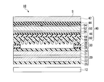
- FIG. 1 is a cross-sectional view showing an example of an image display device of the present invention.
- the image display device 10 of this example fixes the liquid crystal panel 20 as the image display device main body, the touch panel 40 disposed opposite to the image display side of the liquid crystal panel 20 via a gap, and the liquid crystal panel 20 and the touch panel 40.
- the backlight 12 disposed on the side of the liquid crystal panel 20 opposite to the side on which the touch panel 40 is disposed.
- each member will be described.
- the liquid crystal panel 20 of this example includes a first glass substrate 21 on which a color filter (not shown), a transparent electrode (not shown), an alignment film (not shown), etc. are formed, a transparent electrode (not shown), and an alignment film. (Not shown) and the like, a liquid crystal layer 23 sandwiched between the first glass substrate 21 and the second glass substrate 22, and a first side opposite to the liquid crystal layer 23
- the first polarizing film 24 bonded to the surface of the glass substrate 21 via an adhesive layer (not shown) and the adhesive layer (not shown) on the surface of the second glass substrate 22 opposite to the liquid crystal layer 23.
- the second polarizing film 25 bonded to each other via the abbreviation).
- the adhesive for the adhesive layer include known transparent adhesives and transparent pressure-sensitive adhesives used for optical applications.
- the touch panel 40 in this example is a capacitive touch panel that detects the position of a conductor (finger, metal, etc.) approaching or in contact with the input surface S as a change in capacitance, and is a cover glass having the input surface S. 42, the electrode substrate 50 bonded to the opposite side of the input surface S with the cover glass 42 interposed therebetween via an adhesive layer 44, and the transparent electrode of the electrode substrate 50, and electrically connected to the input surface S.
- a detection unit (not shown) that detects a change in capacitance when a body approaches or contacts, and a low reflection film 60 that is bonded to the surface of the electrode substrate 50 via an adhesive layer 46. is there.
- the electrode substrate 50 includes a substrate body 52, a stripe-shaped first transparent electrode 54 formed on one surface of the substrate body 52 and including a plurality of electrode patterns extending in the first direction, and the other of the substrate body 52. And a stripe-shaped second transparent electrode 56 formed of a plurality of electrode patterns extending in a second direction intersecting the first direction.
- the substrate body 52 is made of a transparent plate, film, sheet or the like.
- Examples of the material of the substrate body 52 include glass, acrylic resin, polycarbonate, styrene resin, polyester, cellulose resin (such as triacetyl cellulose), polyolefin, and alicyclic polyolefin.
- the first transparent electrode 54 and the second transparent electrode 56 are thin films that can transmit light and have conductivity.
- Examples of the first transparent electrode 54 and the second transparent electrode 56 include a conductive metal oxide thin film.
- Examples of the conductive metal oxide include indium oxide doped with tin (hereinafter referred to as ITO).
- the detection unit detects, for example, a change in capacitance between the conductor and the electrode when the conductor approaches or contacts the input surface while applying a predetermined voltage to the transparent electrode, and at any location It detects whether the conductor is approaching or touching.
- the low reflection film 60 includes a base film 64 and a cured resin layer 66 formed on the surface of the base film 64 and having a fine concavo-convex structure including a plurality of convex portions 62 on the surface.
- a base film 64 and a cured resin layer 66 formed on the surface of the base film 64 and having a fine concavo-convex structure including a plurality of convex portions 62 on the surface.
- the base film 64 is made of a transparent film.
- Examples of the material of the base film 64 include glass, acrylic resin, polycarbonate, styrene resin, polyester, cellulose resin (such as triacetyl cellulose), polyolefin, and alicyclic polyolefin.
- the cured resin layer 66 is a transparent film made of a cured product of an active energy ray-curable resin composition described later, and has a fine concavo-convex structure made up of a plurality of convex portions 62 on the surface.
- the fine concavo-convex structure (so-called moth-eye structure) in which a plurality of convex portions 62 such as a substantially conical shape and a pyramid shape are arranged effectively reflects the refractive index continuously from the refractive index of air to the refractive index of the material. It is known to be a means of prevention.
- the fine concavo-convex structure is preferably formed by transferring a plurality of pores of anodized alumina described later.
- a fine concavo-convex structure formed by transferring a plurality of pores of anodized alumina can exhibit good low reflectivity. Further, it can be formed at a low cost and can have a large area.
- the average height H of the protrusions 62 is preferably 80 nm or more and 500 nm or less, more preferably 120 nm or more and 400 nm or less, and particularly preferably 150 nm or more and 300 nm or less.
- the average height H of the convex portions 62 is 80 nm or more, the reflectance is sufficiently low and the wavelength dependence of the reflectance is small. If the average height H of the convex part 62 is 500 nm or less, the scratch resistance of the convex part will be good.
- the average height H of the convex portion 62 is obtained by measuring the distance between the top of the convex portion 62 and the bottom of the concave portion existing between the convex portions 62 by electron microscope observation, and averaging these values. It is a thing.
- the period (namely, average interval between the adjacent convex parts 62) P of the convex part 62 is below the wavelength of visible light, ie, 400 nm or less from the point that the reflectance of visible light becomes sufficiently low.
- the period P of the convex part 62 is about 100 nm, and is more preferably 200 nm or less, and particularly preferably 150 nm or less.
- the period P of the protrusions 62 is preferably 20 nm or more from the viewpoint of easy formation of the protrusions 62.
- the period P between the convex portions 62 is measured by measuring the distance between the adjacent convex portions 62 (the distance from the center of the convex portion 62 to the center of the adjacent convex portion 62) by electron microscope observation at 50 points. It is average.
- the aspect ratio of the convex portion 62 (average height H of the convex portion 62 / period P of the convex portion 62) is preferably 0.8 or more and 5.0 or less, more preferably 1.2 or more and 4.0 or less. 5 or more and 3.0 or less are particularly preferable. If the aspect ratio of the convex part 62 is 0.8 or more, the reflectance is sufficiently low. If the aspect ratio of the convex part 62 is 5.0 or less, the scratch resistance of the convex part 62 will be good.
- the shape of the convex portion 62 is a shape in which the convex cross-sectional area in the direction orthogonal to the height direction continuously increases from the outermost surface in the depth direction, that is, the cross-sectional shape in the height direction of the convex portion 62 is a triangle, A trapezoidal shape or a bell-shaped shape is preferable.
- Adhesive layer examples of the adhesive for the adhesive layers 44 and 46 include known transparent adhesives and transparent adhesives used for optical applications.
- the adhesive member 30 fixes the liquid crystal panel 20 and the touch panel 40.
- the adhesive member 30 includes a base material 32, a first adhesive layer 34 laminated on one surface of the base material 32, and a second adhesive layer 36 laminated on the other surface of the base material 32.
- the first pressure-sensitive adhesive layer 34 is in contact with the surface of the liquid crystal panel 20 on the image display side
- the second pressure-sensitive adhesive layer 36 is on the surface of the touch panel 40 having the fine uneven structure.
- the liquid crystal panel 20 and the touch panel 40 are fixed by contact.
- the fixing position of the liquid crystal panel 20 and the touch panel 40 is not particularly limited as long as the liquid crystal panel 20 and the touch panel 40 can be fixed without interfering with the image from the liquid crystal panel 20. preferable.
- the adhesive member 30 has an adhesive strength (W1) between the first pressure-sensitive adhesive layer 34 and the liquid crystal panel 20, a breaking strength (W2) of the first pressure-sensitive adhesive layer, and the first pressure-sensitive adhesive layer 34 and the substrate 32.
- the adhesive strength (W5) with the touch panel 40 is smaller, and the breaking strength (W4) of the base material 32 is larger than at least one of the adhesive strength (W3 ′) and the adhesive strength (W5). It is configured.
- the breaking strength (W4) is smaller than the adhesive strength (W1), the adhesive strength (W3), the adhesive strength (W3 ′), and the adhesive strength (W5), an attempt is made to separate the touch panel 40 and the liquid crystal panel 20 from each other.
- the material 32 will break. Therefore, the broken base material 32 and the first pressure-sensitive adhesive layer 34 remain on the surface of the liquid crystal panel 20, and the remaining broken base material 32 and the second pressure-sensitive adhesive layer 36 remain on the surface of the touch panel 40. .
- the broken nonwoven fabric or polyurethane and the first pressure-sensitive adhesive layer 34 remain on the surface of the liquid crystal panel 20, and the remaining fracture on the surface of the touch panel 40.
- the non-woven fabric or polyurethane and the second pressure-sensitive adhesive layer 36 remain.
- the first pressure-sensitive adhesive layer 34 and the second pressure-sensitive adhesive layer 36 can be wiped off relatively easily.
- the broken base material 32 and the first pressure-sensitive adhesive layer 34 remain on the surface of the liquid crystal panel 20, or when the broken base material 32 and the second pressure-sensitive adhesive layer 36 are on the surface of the touch panel 40. If it remains, if it is wiped off with a cloth impregnated with alcohol or the like, the broken pieces of the base material 32 may damage the surface of the liquid crystal panel 20 or the touch panel 40.
- a part of the broken base material 32 absorbs alcohol or the like, and it becomes difficult to sufficiently remove the first pressure-sensitive adhesive layer 34 and the second pressure-sensitive adhesive layer 36.
- the liquid crystal panel 20 is more expensive than the touch panel 40, it is desired to reduce the removal of the pressure-sensitive adhesive layer and the base material from the liquid crystal panel 20 as much as possible and to reuse them without damaging the surface.
- the pressure-sensitive adhesive member 30 used in the present invention has an adhesive strength (W3) such that the adhesive strength (W1) is smaller than the adhesive strength (W3), the adhesive strength (W3 ′), and the adhesive strength (W5). ) And adhesive strength (W5). Therefore, when the touch panel 40 and the liquid crystal panel 20 are separated, the interface between the first pressure-sensitive adhesive layer 34 and the liquid crystal panel 20 is peeled without the base material 32 being broken, so that the pressure-sensitive adhesive member 30 is moved to the touch panel 40 side. The touch panel 40 and the liquid crystal panel 20 can be easily separated in a state of being attached.
- the adhesive member 30 is unlikely to remain on the liquid crystal panel 20 side, and even if it remains, it can be easily removed because it is only a trace (residue residue) of the first adhesive layer 34, and the surface of the liquid crystal panel 20 is removed at the time of removal. Can be prevented from being damaged. Further, since it can be easily predicted whether the adhesive member 30 remains on the surface of the touch panel 40 or the liquid crystal panel 20 without actually separating, the adhesive member 30 can be removed more easily.
- the pressure-sensitive adhesive member 30 used in the present invention is configured such that the breaking strength (W4) is larger than at least one of the adhesive strength (W3 ′) and the adhesive strength (W5). Therefore, when the adhesive member 30 remaining on the surface of the touch panel 40 is to be peeled off, it is considered that the base material 32 is not broken and becomes any of the following (i) to (iii). (I) When the adhesive strength (W5) is the smallest among the adhesive strength (W3), the adhesive strength (W3 ′), and the adhesive strength (W5), peeling occurs at the interface between the second pressure-sensitive adhesive layer 36 and the touch panel 40.
- the adhesive member 30 is unlikely to remain on the surface of the touch panel 40, and even if it remains, it is about the trace (adhesive residue) of the second adhesive layer 36.
- the second pressure-sensitive adhesive layer 36 remains on the surface of the touch panel 40.
- the second pressure-sensitive adhesive layer 36 can be wiped using a cloth impregnated with alcohol or the like. is there. Therefore, in the case of (i) and (ii) above, the second pressure-sensitive adhesive layer 36 can be removed by wiping the surface of the touch panel 40 after peeling with alcohol or the like. In particular, the above (i) can be removed more easily because the trace of the second pressure-sensitive adhesive layer 36 is removed.
- the breaking strength (W4) is larger than at least one of the adhesive strength (W3 ′) and the adhesive strength (W5), the second pressure-sensitive adhesive layer 36 and the base material 32 remaining on the surface of the touch panel 40 are to be peeled off.
- the base material 32 is considered to be the following (iv) or (v) without breaking.
- the adhesive member 30 is unlikely to remain on the surface of the touch panel 40, and even if it remains, it is about the trace (adhesive residue) of the second adhesive layer 36.
- the second adhesive layer 36 remains on the surface of the touch panel 40. Therefore, as in the cases (i) and (ii) above, the second pressure-sensitive adhesive layer 36 can be removed by wiping the surface of the touch panel 40 after peeling with alcohol or the like.
- the breaking strength (W4) is preferably larger than the adhesive strength (W3 ′) and the adhesive strength (W5). Moreover, it is preferable that breaking strength (W4) is larger than adhesive strength (W3). Furthermore, the adhesive strength (W5) is preferably smaller than the adhesive strength (W3) and the adhesive strength (W3 ′). If the adhesive strength (W5) is smaller than the adhesive strength (W3) and the adhesive strength (W3 ′), the adhesive member 30 is peeled off from the touch panel 40, so that the above (i) is obtained. 30 hardly remains, and even if it remains, it is about the trace (residue residue) of the second pressure-sensitive adhesive layer 36, and the second pressure-sensitive adhesive layer 36 can be removed more easily.
- the adhesive member 30 has the smallest adhesive strength (W1) among the adhesive strength (W1), the adhesive strength (W3), the adhesive strength (W3 ′), the adhesive strength (W5), and the breaking strength (W4). It is preferable that the adhesive strength (W5) is small and the breaking strength (W4) is the largest. That is, it is preferable to satisfy the relationship of “adhesive strength (W1) ⁇ adhesive strength (W5) ⁇ adhesive strength (W3), adhesive strength (W3 ′) ⁇ breaking strength (W4)”.
- the relationship between the adhesive strength (W3) and the adhesive strength (W3 ′) is not particularly limited, and the adhesive strength (W3) and the adhesive strength (W3 ′) may be the same value, or the adhesive strength ( W3) may be greater or the adhesive strength (W3 ′) may be greater.
- the breaking strength W4 of the substrate 30 is F1
- the peeling force between the touch panel 40 and the adhesive member 30 is F2
- the peeling force between the liquid crystal panel 20 and the adhesive member 30 is F3, F3 ⁇ F2
- the laminate is configured so that the relationship ⁇ F1 is satisfied.
- the liquid crystal panel 20 and the touch panel 40 fixed by the adhesive member 30 can be easily separated. Moreover, since the base material 32 is not easily broken when the adhesive member 30 remaining on the surface of the touch panel 40 is peeled off, even if the second adhesive layer 36 remains on the surface of the touch panel 40, it can be easily removed.
- the 1st adhesive layer 34 and the 2nd adhesive layer 36 remain on the surface of the liquid crystal panel 20 or the touch panel 40, these can be wiped off using ethanol, isobutyl alcohol, isopropyl alcohol, etc. .
- the adhesive strength (W1) is preferably 1 N / 10 mm or more and 13 N / 10 mm or less. By setting the adhesive strength (W1) to 1 N / 10 mm or more, the liquid crystal panel 20 and the touch panel 40 can be sufficiently fixed. On the other hand, the liquid crystal panel 20 and the touch panel 40 can be easily separated by setting the adhesive strength (W1) to 13 N / mm or less.
- the adhesive strength (W1) is determined according to JIS Z 0237: 2009 (ISO 29862 and ISO 29863). Specifically, after the adhesive member 30 is attached to the surface of the liquid crystal panel 20 on which the image is displayed, the force required when the adhesive member 30 is peeled 180 ° from the surface of the liquid crystal panel 20 ( It is calculated
- the adhesive strength (W5) is preferably 3 N / 10 mm or more and 15 N / 10 mm or less (provided that the adhesive strength (W5) is greater than the adhesive strength (W1)).
- the adhesive strength (W5) is more preferably 4 N / 10 mm or more and 14.5 N / 10 mm or less, and more preferably 5 N / 10 mm or more and 14 N / 10 mm or less.
- Adhesive strength (W5) is determined according to JIS Z 0237: 2009 (ISO 29862 and ISO 29863). Specifically, after sticking the adhesive member 30 to the low reflection film 60, the force (peeling force) required when peeling the adhesive member 30 from the surface of the low reflection film 60 at 180 ° is measured. Is required.
- the adhesive strength (W3), adhesive strength (W3 '), and breaking strength (W4) are not particularly limited as long as the pressure-sensitive adhesive member 30 has the above-described configuration.
- the adhesive strength (W3) is determined according to JIS Z 0237: 2009 (ISO 29862 and ISO 29863). Specifically, it is obtained by measuring a force (peeling force) required when the first pressure-sensitive adhesive layer 34 of the pressure-sensitive adhesive member 30 is peeled away from the surface of the substrate 32 by 180 °. Similarly, the adhesive strength (W3 ′) can also be obtained by measuring a force (peeling force) required when the second pressure-sensitive adhesive layer 36 is peeled away from the surface of the base material 32 at 180 °.
- the breaking strength (W4) is obtained by measuring a force (cutting force) required when the substrate 32 is pulled and cut in the thickness direction. Even if the cutting force is not measured, if the adhesive member 30 is peeled from the touch panel 40 and the base material 32 of the adhesive member 30 is not broken, the breaking strength (W4) is the adhesive strength (W3 ′). And it can be judged that it is larger than at least one of adhesive strength (W5).
- the adhesive strength (W1), adhesive strength (W3), adhesive strength (W3 ′), adhesive strength (W5), and breaking strength (W4) are, for example, the type of the substrate 32, the first pressure-sensitive adhesive layer 34, The pressure-sensitive adhesive layer 36 can be adjusted according to the type of pressure-sensitive adhesive.
- the substrate 32 is not particularly limited as long as it has a breaking strength (W4) larger than at least one of the adhesive strength (W3 ′) and the adhesive strength (W5).
- PET substrate polyethylene terephthalate substrate
- PCT substrate polycarbonate substrate.
- the adhesive strength (W1) is smaller than the adhesive strength (W3), the adhesive strength (W3 ′), and the adhesive strength (W5).
- W3 the adhesive strength
- W5 the adhesive strength
- an acrylic adhesive, a urethane adhesive, a silicone adhesive, a rubber adhesive, etc. are mentioned.
- the kind of adhesive may be changed by the 1st adhesive layer 34 and the 2nd adhesive layer 36, and the same kind of adhesive may be used.
- the pressure-sensitive adhesive examples include (meth) acrylic pressure-sensitive adhesives, urethane-based pressure-sensitive adhesives, synthetic rubber-based pressure-sensitive adhesives, natural rubber-based pressure-sensitive adhesives, and silicone-based pressure-sensitive adhesives, but (meth) acrylate alone or (meth) A (meth) acrylic adhesive composition in which an acrylic copolymer comprising a copolymer of acrylate and another monomer is used as a base polymer, and additives such as a tackifier resin and a crosslinking agent are blended as necessary Can preferably be used.
- Examples of the (meth) acrylate having 1 to 12 carbon atoms include methyl (meth) acrylate, ethyl (meth) acrylate, n-butyl (meth) acrylate, isobutyl (meth) acrylate, t-butyl (meth) acrylate, n Monomers such as -hexyl (meth) acrylate, n-octyl (meth) acrylate, isooctyl (meth) acrylate, isononyl (meth) acrylate, cyclohexyl (meth) acrylate, 2-ethylhexyl (meth) acrylate, etc. Species or two or more are used.
- (meth) acrylates having 4 to 12 carbon atoms in the alkyl group are preferable, and (meth) acrylates having a linear or branched structure having 4 to 8 carbon atoms are more preferable.
- n-butyl acrylate is preferable because it is easy to ensure adhesion to the adherend and has excellent cohesive strength and resistance to sebum.
- the content of the (meth) acrylate having 1 to 12 carbon atoms in the acrylic copolymer is preferably 80% by mass or more and 98.5% by mass or less in the monomer component constituting the acrylic copolymer, More preferably, it is 90 mass% or more and 98.5 mass% or less.
- the acrylic copolymer used in the present invention may be copolymerized with a highly polar vinyl monomer.
- the highly polar vinyl monomer include a vinyl monomer having a hydroxyl group, a vinyl monomer having a carboxyl group, and a vinyl having an amide group.
- a monomer etc. are mentioned, These 1 type (s) or 2 or more types are used.
- Examples of the monomer having a hydroxyl group include hydroxyl groups such as 2-hydroxyethyl (meth) acrylate, 2-hydroxypropyl (meth) acrylate, 4-hydroxybutyl (meth) acrylate, 6-hydroxyhexyl (meth) acrylate and the like ( A (meth) acrylate can be used.
- vinyl monomer having a carboxyl group acrylic acid, methacrylic acid, itaconic acid, maleic acid, (meth) acrylic acid dimer, crotonic acid, ethylene oxide-modified succinic acid acrylate, etc. can be used. It is preferable to use it as a polymerization component.
- Examples of the monomer having an amide group include N-vinylpyrrolidone, N-vinylcaprolactam, acryloylmorpholine, acrylamide, N, N-dimethylacrylamide and the like.
- Examples of other highly polar vinyl monomers include sulfonic acid group-containing monomers such as vinyl acetate, ethylene oxide-modified succinic acid acrylate, and 2-acrylamido-2-methylpropanesulfonic acid.
- the content of the highly polar vinyl monomer is preferably 1.5% by mass or more and 20% by mass or less, and 1.5% by mass or more and 10% by mass or less in the monomer component constituting the acrylic copolymer. Is more preferable, and it is still more preferable that they are 2 mass% or more and 8 mass% or less. By containing in the said range, it is easy to adjust the cohesion force, holding force, and adhesiveness of an adhesive to a suitable range.
- the vinyl monomer having a functional group that reacts with it is preferably a hydroxyl group-containing vinyl monomer, such as 2-hydroxyethyl (meth) acrylate or 4-hydroxybutyl (meth) acrylate. 6-hydroxyhexyl (meth) acrylate is particularly preferred.
- the content of the hydroxyl group-containing vinyl monomer that reacts with the isocyanate crosslinking agent is preferably 0.01% by mass or more and 1.0% by mass or less of the monomer component constituting the acrylic copolymer, and is 0.03% by mass. The content is particularly preferably 0.3% by mass or less.
- the acrylic copolymer can be obtained by copolymerization by a known polymerization method such as a solution polymerization method, a cage polymerization method, a suspension polymerization method, or an emulsion polymerization method.
- a combination method or a bulk polymerization method is preferred.
- Polymerization can be initiated by peroxides such as benzoyl peroxide and lauroyl peroxide, thermal initiation using azo-based thermal polymerization initiators such as azobisisobutylnitrile, acetophenone-based, benzoin ether-based, benzyl
- azo-based thermal polymerization initiators such as azobisisobutylnitrile, acetophenone-based, benzoin ether-based, benzyl
- a starting method by ultraviolet irradiation using a ketal-based, acylphosphine oxide-based, benzoin-based or benzophenone-based photopolymerization initiator, or a method by electron beam irradiation can be arbitrarily selected.
- the weight average molecular weight in terms of standard polystyrene measured by gel permeation chromatography is 400,000 to 3 million, preferably 800,000 to 2.5 million. .
- a tackifying resin in order to improve the adhesion to the adherend and the surface adhesion strength.
- Tackifying resins include rosin, polymerized rosin, polymerized rosin ester, rosin phenol, stabilized rosin ester, disproportionated rosin ester, hydrogenated rosin ester, terpene, terpene phenol, petroleum resin Examples thereof include (meth) acrylate resins and the like.
- an emulsion-type tackifying resin When used in an emulsion-type pressure-sensitive adhesive composition, it is preferable to use an emulsion-type tackifying resin.
- the blending ratio when using the acrylic copolymer and the tackifier resin is preferably such that the content of the tackifier resin with respect to 100 parts by mass of the acrylic copolymer is 5 parts by mass or more and 60 parts by mass or less. It is preferable that they are 8 mass parts or more and 50 mass parts or less. By setting the ratio between the two in this range, it becomes easy to ensure adhesion with the adherend.
- the acrylic pressure-sensitive adhesive composition it is preferable to crosslink the pressure-sensitive adhesive in order to increase the cohesive strength of the pressure-sensitive adhesive layer.
- a crosslinking agent include an isocyanate crosslinking agent, an epoxy crosslinking agent, a metal chelate crosslinking agent, and an aziridine crosslinking agent.
- a crosslinking agent of a type that is added after the completion of polymerization and causes the crosslinking reaction to proceed is preferable, and an isocyanate-based crosslinking agent and an epoxy-based crosslinking agent that are highly reactive with a (meth) acrylic copolymer are preferable.
- An isocyanate-based cross-linking agent is more preferable because adhesion to the substrate is improved.
- Examples of the isocyanate-based crosslinking agent include tolylene diisocyanate, naphthylene-1,5-diisocyanate, hexamethylene diisocyanate, diphenylmethane diisocyanate, xylylene diisocyanate, trimethylolpropane-modified tolylene diisocyanate, and the like. Particularly preferred are trifunctional polyisocyanate compounds. Examples of the trifunctional isocyanate compound include tolylene diisocyanate, trimethylolpropane adducts thereof, and triphenylmethane isocyanate.
- the value of the gel fraction for measuring the insoluble content after the pressure-sensitive adhesive layer is immersed in toluene for 24 hours is used.
- the gel fraction is preferably 25% by mass or more and 70% by mass or less. More preferably, the cohesiveness and the adhesiveness are good within the range of 30% by mass or more and 60% by mass or less, more preferably 30% by mass or more and 55% by mass or less.
- Additives for adhesives such as plasticizers, softeners, antioxidants, flame retardants, fillers such as glass and plastic fibers / balloons / beads, metal powders, metal oxides, metal nitrides Colorants such as pigments and dyes, leveling agents, thickeners, water repellents, antifoaming agents and the like can be optionally added to the pressure-sensitive adhesive composition.
- the above-described low reflection film 60 is provided on the surface of the touch panel 40 facing the liquid crystal panel 20.
- the low reflection film 60 having a fine concavo-convex structure with a period P of 400 nm or less on the surface has a higher adhesive strength when the pressure-sensitive adhesive layer is attached as compared with a film having a smooth surface. This is presumably because the convex portions of the fine concavo-convex structure bite into the pressure-sensitive adhesive layer, and the contact area with the pressure-sensitive adhesive layer is greatly increased as compared with a smooth film. That is, as shown in FIG. 1, the low reflection film 60 is provided on the surface of the touch panel 40 facing the liquid crystal panel, thereby preventing reflection at the interface and improving the visibility of the image display device, as well as the adhesive strength. It becomes possible to make (W5) larger than the adhesive strength (W1).
- the type of the pressure-sensitive adhesive is changed between the first pressure-sensitive adhesive layer 34 and the second pressure-sensitive adhesive layer 36, or the adhesive strength is adjusted. Without doing so, the adhesive strength (W1) and the adhesive strength (W5) can be adjusted. Therefore, the image display device 10 can be assembled without worrying about the front and back of the adhesive member 30, and the image display device 10 can be manufactured with high yield.
- the low reflection film 60 is manufactured as follows using, for example, a manufacturing apparatus shown in FIG.
- the active energy ray-curable resin composition 74 is supplied from the tank 72 between the surface 64 and the surface 64.
- the base film 64 and the active energy ray curable resin composition 74 are nipped between the mold 70 and the nip roll 78 whose nip pressure is adjusted by the pneumatic cylinder 76, and the active energy ray curable resin composition 74 is
- the base film 64 and the mold 70 are uniformly distributed, and at the same time, the pores of the mold 70 are filled.
- the active energy ray curable resin composition 74 sandwiched between the mold 70 and the base film 64, the active energy ray irradiation device 80 installed below the mold 70 is used, and the base film 64 side
- the active energy ray-curable resin composition 74 is irradiated with active energy rays to cure the active energy ray-curable resin composition 74, thereby transferring a plurality of protrusions on which a plurality of pores on the surface of the mold 70 are transferred.
- a cured resin layer 66 having a fine concavo-convex structure consisting of parts (not shown) on the surface is formed.
- the low reflection film 60 is obtained by peeling the base film 64 having the cured resin layer 66 formed on the surface by the peeling roll 82.
- the active energy ray irradiation device 80 As the active energy ray irradiation device 80, a high-pressure mercury lamp, a metal halide lamp, or the like is preferable. Cumulative amount of light is, 100 mJ / cm 2 or more 10000 mJ / cm 2 or less.
- the mold 70 is a mold having anodized alumina on the surface.
- a mold having an anodized alumina on the surface can have a large area and is easy to manufacture.
- Anodized alumina is a porous oxide film (alumite) of aluminum and has a plurality of pores on the surface.
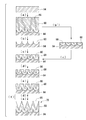
- a mold having an anodized alumina on its surface can be produced, for example, through the following steps (a) to (f).
- a step of forming an oxide film by anodizing an aluminum substrate in an electrolytic solution (B) A step of removing all of the oxide film to form pore generation points for anodic oxidation. (C) A step of anodizing the aluminum substrate again in the electrolytic solution to form an oxide film having pores at the pore generation points. (D) A step of enlarging the diameter of the pores. (E) A step of anodizing again in the electrolytic solution after the step (d). (F) A step of repeatedly performing the step (d) and the step (e).
- the purity of aluminum is preferably 99% or more, more preferably 99.5% or more, and particularly preferably 99.8% or more. When the purity of aluminum is low, when anodized, an uneven structure having a size to scatter visible light may be formed due to segregation of impurities, or the regularity of pores obtained by anodization may be lowered.
- the electrolytic solution include sulfuric acid, an oxalic acid aqueous solution, and a phosphoric acid aqueous solution.
- Examples of the method for removing the oxide film include a method in which aluminum is not dissolved but dissolved in a solution that selectively dissolves the oxide film and removed.
- Examples of such a solution include a chromic acid / phosphoric acid mixed solution.
- Examples of the electrolytic solution include the same as in step (a).
- the pore diameter expansion treatment is a treatment for expanding the diameter of the pores obtained by anodic oxidation by immersing in a solution dissolving the oxide film. Examples of such a solution include a phosphoric acid aqueous solution of about 1 mol / L.
- Examples of the electrolytic solution include the same as in step (a).
- a mold 70 on which anodized alumina (aluminum porous oxide film (alumite)) is formed is obtained. It is preferable that the last end is step (d).
- the total number of repetitions is preferably 3 times or more, and more preferably 5 times or more. When the number of repetitions is 2 or less, the diameter of the pores decreases discontinuously, and therefore the effect of reducing the reflectance of the cured resin layer 66 formed using such anodized alumina having such pores is insufficient. is there.
- the surface of the anodized alumina may be treated with a release agent so that separation from the cured resin layer 66 is easy.
- the treatment method include a method of coating a silicone resin or a fluorine-containing polymer, a method of depositing a fluorine-containing compound, and a method of coating a fluorine-containing silane compound.
- Examples of the shape of the pore 86 include a substantially conical shape, a pyramid shape, a cylindrical shape, and the like. A shape that continuously decreases in the direction is preferred.
- the average depth of the pores 86 is preferably 80 nm or more and 500 nm or less, more preferably 120 nm or more and 400 nm or less, and particularly preferably 150 nm or more and 300 nm or less.
- the period of the pores 86 (average interval between adjacent pores) is not more than the wavelength of visible light, that is, not more than 400 nm, preferably not more than 200 nm, and more preferably not more than 150 nm.
- the periodic interval of the pores 86 is preferably 20 nm or more.
- the aspect ratio of the pores 86 (average pore depth / pore cycle) is preferably 0.8 or more and 5.0 or less, more preferably 1.2 or more and 4.0 or less, and 1.5 or more and 3. 0 or less is particularly preferable.
- the surface of the cured resin layer 66 formed by transferring the pores 86 as shown in FIG. 4 has a so-called moth-eye structure.
- the manufacturing method of a mold is not limited to the method mentioned above, For example, it may replace with a process (b) and may perform the following process (b ').
- the pores 86 of the oxide film 88 formed in the step (a) have a variation in the interval. Therefore, in the step (b ′), the portion where the regularity is disturbed is removed (that is, the surface of the oxide film 88 is removed until there is no variation in the interval between the pores 86).
- the pores 86 exposed on the surface in the step (b ′) serve as the pore generation points 90 in the step (b).
- the oxide film 88 may be dissolved using a chromic acid / phosphoric acid mixed solution or a phosphoric acid solution.
- the active energy ray-curable resin composition contains a polymerizable compound and a polymerization initiator.
- the polymerizable compound include monomers, oligomers, and reactive polymers having a radical polymerizable bond and / or a cationic polymerizable bond in the molecule.
- the active energy ray-curable resin composition may contain a non-reactive polymer and an active energy ray sol-gel reactive composition.
- Examples of the monomer having a radical polymerizable bond include a monofunctional monomer and a polyfunctional monomer.
- Monofunctional monomers include methyl (meth) acrylate, ethyl (meth) acrylate, propyl (meth) acrylate, n-butyl (meth) acrylate, i-butyl (meth) acrylate, s-butyl (meth) acrylate, t- Butyl (meth) acrylate, 2-ethylhexyl (meth) acrylate, lauryl (meth) acrylate, alkyl (meth) acrylate, tridecyl (meth) acrylate, stearyl (meth) acrylate, cyclohexyl (meth) acrylate, benzyl (meth) acrylate, Phenoxyethyl (meth) acrylate, isobornyl (meth) acrylate, glycidyl (meth
- Polyfunctional monomers include ethylene glycol di (meth) acrylate, tripropylene glycol di (meth) acrylate, isocyanuric acid ethylene oxide modified di (meth) acrylate, triethylene glycol di (meth) acrylate, diethylene glycol di (meth) acrylate , Neopentyl glycol di (meth) acrylate, 1,6-hexanediol di (meth) acrylate, 1,5-pentanediol di (meth) acrylate, 1,3-butylene glycol di (meth) acrylate, polybutylene glycol di (Meth) acrylate, 2,2-bis (4- (meth) acryloxypolyethoxyphenyl) propane, 2,2-bis (4- (meth) acryloxyethoxyphenyl) propane, 2,2-bis (4- (3- (Meth) acryloxy-2-hydroxypropoxy) phenyl) propane, 1,2-bis (3- (meth) acryloxy-2-hydroxypropoxy
- Examples of the monomer having a cationic polymerizable bond include monomers having an epoxy group, an oxetanyl group, an oxazolyl group, a vinyloxy group, and the like, and a monomer having an epoxy group is particularly preferable.
- oligomer or reactive polymer examples include unsaturated polyesters such as a condensate of unsaturated dicarboxylic acid and polyhydric alcohol; polyester (meth) acrylate, polyether (meth) acrylate, polyol (meth) acrylate, epoxy (meth) Examples thereof include acrylates, urethane (meth) acrylates, cationic polymerization type epoxy compounds, homopolymers of the above-described monomers having a radical polymerizable bond in the side chain, and copolymerized polymers.
- unsaturated polyesters such as a condensate of unsaturated dicarboxylic acid and polyhydric alcohol
- non-reactive polymers examples include acrylic resins, styrene resins, polyurethanes, cellulose resins, polyvinyl butyral, polyesters, thermoplastic elastomers, and the like.
- active energy ray sol-gel reactive composition examples include alkoxysilane compounds and alkyl silicate compounds.
- R 11 x Si (OR 12 ) y (1) As an alkoxysilane compound, the compound of following formula (1) is mentioned.
- alkoxysilane compound examples include tetramethoxysilane, tetra-i-propoxysilane, tetra-n-propoxysilane, tetra-n-butoxysilane, tetra-s-butoxysilane, tetra-t-butoxysilane, methyltriethoxysilane, Examples include methyltripropoxysilane, methyltributoxysilane, dimethyldimethoxysilane, dimethyldiethoxysilane, trimethylethoxysilane, trimethylmethoxysilane, trimethylpropoxysilane, and trimethylbutoxysilane.
- alkyl silicate compound examples include a compound of the following formula (2).
- R 21 to R 24 each represents an alkyl group having 1 to 5 carbon atoms, and z represents an integer of 3 to 20.
- alkyl silicate compound examples include methyl silicate, ethyl silicate, isopropyl silicate, n-propyl silicate, n-butyl silicate, n-pentyl silicate, acetyl silicate and the like.
- examples of the photopolymerization initiator include benzoin, benzoin methyl ether, benzoin ethyl ether, benzoin isopropyl ether, benzoin isobutyl ether, benzyl, benzophenone, p-methoxybenzophenone, 2,2-diethoxy.
- examples of the polymerization initiator include benzophenone, 4,4-bis (diethylamino) benzophenone, 2,4,6-trimethylbenzophenone, methyl orthobenzoylbenzoate, 4-phenylbenzophenone, t- Thioxanthones such as butylanthraquinone, 2-ethylanthraquinone, 2,4-diethylthioxanthone, isopropylthioxanthone, 2,4-dichlorothioxanthone; diethoxyacetophenone, 2-hydroxy-2-methyl-1-phenylpropan-1-one, benzyl Dimethyl ketal, 1-hydroxycyclohexyl-phenyl ketone, 2-methyl-2-morpholino (4-thiomethylphenyl) propan-1-one, 2-benzyl-2-dimethylamino-1- (4-morpho Benzophene ether such as benzoin methyl ether, benzo
- thermal polymerization initiator examples include methyl ethyl ketone peroxide, benzoyl peroxide, dicumyl peroxide, t-butyl hydroperoxide, cumene hydroperoxide, t-butyl peroxy octoate, organic peroxides such as t-butylperoxybenzoate and lauroyl peroxide; azo compounds such as azobisisobutyronitrile; N, N-dimethylaniline, N, N-dimethyl-p- Examples thereof include a redox polymerization initiator combined with an amine such as toluidine.
- the active energy ray-curable resin composition may contain an antistatic agent, a release agent, an additive such as a fluorine compound for improving the antifouling property; fine particles, and a small amount of solvent, if necessary.
- an active energy ray-curable resin composition capable of forming a hydrophobic material is used. It is preferable to use a composition containing a fluorine-containing compound or a silicone compound.
- Fluorine-containing compounds As the fluorine-containing compound, a compound having a fluoroalkyl group represented by the following formula (3) is preferable. -(CF 2 ) n -X (3).
- X represents a fluorine atom or a hydrogen atom
- n represents an integer of 1 or more, preferably 1 to 20, more preferably 3 to 10, and particularly preferably 4 to 8.
- Fluorine-containing compounds include fluorine-containing monomers, fluorine-containing silane compounds, fluorine-containing surfactants, fluorine-containing polymers, and the like.
- fluorine-containing monomer examples include a fluoroalkyl group-substituted vinyl monomer and a fluoroalkyl group-substituted ring-opening polymerizable monomer.
- fluoroalkyl group-substituted vinyl monomer examples include fluoroalkyl group-substituted (meth) acrylates, fluoroalkyl group-substituted (meth) acrylamides, fluoroalkyl group-substituted vinyl ethers, and fluoroalkyl group-substituted styrenes.
- fluoroalkyl group-substituted ring-opening polymerizable monomer examples include fluoroalkyl group-substituted epoxy compounds, fluoroalkyl group-substituted oxetane compounds, and fluoroalkyl group-substituted oxazoline compounds.
- a fluoroalkyl group-substituted (meth) acrylate is preferable, and a compound of the following formula (4) is particularly preferable.
- CH 2 C (R 41 ) C (O) O— (CH 2 ) m — (CF 2 ) n —X (4).
- R 41 represents a hydrogen atom or a methyl group
- X represents a hydrogen atom or a fluorine atom
- m represents an integer of 1 to 6, preferably 1 to 3, more preferably 1 or 2
- n represents an integer of 1 or more, preferably 1 to 20, more preferably 3 to 10, and particularly preferably 4 to 8.
- fluorine-containing silane compound a fluoroalkyl group-substituted silane compound is preferable, and a compound of the following formula (5) is particularly preferable.
- R f represents a fluorine-substituted alkyl group having 1 to 20 carbon atoms which may contain one or more ether bonds or ester bonds.
- R f include 3,3,3-trifluoropropyl group, tridecafluoro-1,1,2,2-tetrahydrooctyl group, 3-trifluoromethoxypropyl group, and 3-trifluoroacetoxypropyl group. It is done.
- R 51 represents an alkyl group having 1 to 10 carbon atoms.
- examples of R 51 include a methyl group, an ethyl group, and a cyclohexyl group.
- Y represents a hydroxyl group or a hydrolyzable group.
- the hydrolyzable group include an alkoxy group, a halogen atom, and R 52 C (O) O (wherein R 52 represents a hydrogen atom or an alkyl group having 1 to 10 carbon atoms).
- alkoxy group examples include methoxy group, ethoxy group, propyloxy group, i-propyloxy group, butoxy group, i-butoxy group, t-butoxy group, pentyloxy group, hexyloxy group, cyclohexyloxy group, heptyloxy group, Examples include octyloxy group, 2-ethylhexyloxy group, nonyloxy group, decyloxy group, 3,7-dimethyloctyloxy group, lauryloxy group and the like.
- halogen atom examples include Cl, Br, I and the like.
- R 52 C (O) O examples include CH 3 C (O) O, C 2 H 5 C (O) O, and the like.
- Fluorine-containing silane coupling agents include 3,3,3-trifluoropropyltrimethoxysilane, 3,3,3-trifluoropropyltriacetoxysilane, dimethyl-3,3,3-trifluoropropylmethoxysilane, Examples include decafluoro-1,1,2,2-tetrahydrooctyltriethoxysilane.
- fluorine-containing surfactant examples include a fluoroalkyl group-containing anionic surfactant and a fluoroalkyl group-containing cationic surfactant.
- fluoroalkyl group-containing anionic surfactant examples include a fluoroalkylcarboxylic acid having 2 to 10 carbon atoms or a metal salt thereof, disodium perfluorooctanesulfonylglutamate, 3- [omega-fluoroalkyl (C 6 -C 11 ) oxy.
- fluoroalkyl group-containing cationic surfactant examples include aliphatic quaternary compounds such as fluoroalkyl group-containing aliphatic primary, secondary or tertiary amine acids, and perfluoroalkyl (C 6 -C 10 ) sulfonamidopropyltrimethylammonium salts. Examples thereof include ammonium salts, benzalkonium salts, benzethonium chloride, pyridinium salts, imidazolinium salts, and the like.
- Fluorine-containing polymers include polymers of fluoroalkyl group-containing monomers, copolymers of fluoroalkyl group-containing monomers and poly (oxyalkylene) group-containing monomers, and copolymers of fluoroalkyl group-containing monomers and crosslinking reactive group-containing monomers. A polymer etc. are mentioned.
- the fluorine-containing polymer may be a copolymer with another copolymerizable monomer.
- fluorine-containing polymer a copolymer of a fluoroalkyl group-containing monomer and a poly (oxyalkylene) group-containing monomer is preferable.
- poly (oxyalkylene) group a group represented by the following formula (6) is preferable.
- -(OR 61 ) p- (6) R 61 represents an alkylene group having 2 to 4 carbon atoms, and p represents an integer of 2 or more. Examples of R 61 include —CH 2 CH 2 —, —CH 2 CH 2 CH 2 —, —CH (CH 3 ) CH 2 —, —CH (CH 3 ) CH (CH 3 ) —, and the like.
- the poly (oxyalkylene) group may be composed of the same oxyalkylene unit (OR 61 ) or may be composed of two or more oxyalkylene units (OR 61 ).
- the arrangement of two or more oxyalkylene units (OR 61 ) may be a block or random.
- Silicone compounds examples include (meth) acrylic acid-modified silicone, silicone resin, silicone silane coupling agent and the like.
- examples of the (meth) acrylic acid-modified silicone include silicone (di) (meth) acrylates such as X-22-1602 (manufactured by Shin-Etsu Chemical Co., Ltd.).
- hydrophilicity specifically, the contact angle of water is 25 ° or less
- an active energy ray-curable resin composition capable of forming a hydrophilic material It is preferable to use a polyfunctional (meth) acrylate having 4 or more functional groups, a hydrophilic (meth) acrylate having 2 or more functional groups, and a monofunctional monomer as required.
- tetrafunctional or higher polyfunctional (meth) acrylates examples include ditrimethylolpropane tetra (meth) acrylate, pentaerythritol tetra (meth) acrylate, pentaerythritol ethoxytetra (meth) acrylate, dipentaerythritol hydroxypenta (meth) acrylate, di Pentaerythritol hexa (meth) acrylate, succinic acid / trimethylolethane / acrylic acid molar mixture 1: 2: 4 condensation reaction mixture, urethane acrylates (manufactured by Daicel-Cytec: EBECRYL220, EBECRYL1290K, EBECRYL1290K, EBECRYL5129, EBECRYL8210, EBECRYL 8301, KRM 8200), polyether acrylates (manufactured by Daicel-Cytec:
- Long-chain polyethylene such as Aronix M-240, Aronix M260 (manufactured by Toagosei Co., Ltd.), NK ester AT-20E, NK ester ATM-35E (manufactured by Shin-Nakamura Chemical Co., Ltd.)
- polyfunctional acrylates having glycol and polyethylene glycol dimethacrylate. These may be used alone or in combination of two or more.
- polyethylene glycol dimethacrylate the total of the average repeating units of polyethylene glycol chains present in one molecule is preferably 6 to 40, more preferably 9 to 30, and particularly preferably 12 to 20.
- the average repeating unit of the polyethylene glycol chain is 6 or more, the hydrophilicity is sufficient and the antifouling property is improved.
- the average repeating unit of the polyethylene glycol chain is 40 or less, the compatibility with a polyfunctional (meth) acrylate having 4 or more functionalities is improved, and the active energy ray-curable resin composition is hardly separated.
- hydrophilic monofunctional monomers examples include monofunctional (meth) acrylates having a polyethylene glycol chain in the ester group such as M-20G, M-90G, and M-230G (manufactured by Shin-Nakamura Chemical Co., Ltd.), hydroxyalkyl (meth) acrylates, etc. And cationic monomers such as monofunctional (meth) acrylates having a hydroxyl group in the ester group, monofunctional acrylamides, methacrylamidopropyltrimethylammonium methyl sulfate, and methacryloyloxyethyltrimethylammonium methyl sulfate.
- viscosity modifiers such as acryloyl morpholine and vinyl pyrrolidone
- adhesive improvement agents such as acryloyl isocyanate which improves the adhesiveness to a base material, etc.
- the monofunctional monomer may be blended into the active energy ray-curable resin composition as a polymer having a low polymerization degree obtained by (co) polymerizing one or more kinds.
- a polymer having a low degree of polymerization 40/60 of monofunctional (meth) acrylates having a polyethylene glycol chain in an ester group such as M-230G (manufactured by Shin-Nakamura Chemical Co., Ltd.) and methacrylamide propyltrimethylammonium methyl sulfate.
- Copolymer oligomer MRC Unitech Co., Ltd., MG polymer
- the electrode substrate 50 is formed, for example, by depositing ITO or the like on the surface of the substrate body 52 to form a transparent conductive film, and then patterning into a desired electrode pattern to form the first transparent electrode 54 and the second transparent electrode 56. Can be manufactured.
- the touch panel 40 has a fine concavo-convex structure with a period of 400 nm or less on the surface facing the liquid crystal panel 20 (image display device main body), the liquid crystal panel 20 and the touch panel 40 face each other. Reflection of light on the surface is suppressed.
- the liquid crystal panel 20 and the touch panel 40 are fixed by the adhesive member 30 described above. Therefore, the liquid crystal panel 20 and the touch panel 40 can be easily separated when necessary, and the adhesive member 30 can be easily removed from the surface of the touch panel 40. Thereby, when the affixing position of the touch panel 40 and the liquid crystal panel 20 is shifted, the fixed touch panel 40 and the liquid crystal panel 20 are easily separated from each other, and the touch panel 40 and the liquid crystal panel 20 are disposed without being discarded. With this positional relationship, the touch panel 40 and the liquid crystal panel 20 can be pasted again.
- the fixed touch panel 40 and the liquid crystal panel 20 are easily separated from each other, and the member in which the defect is found is removed. It can be easily replaced.
- the liquid crystal panel 20 and the touch panel 40 can be easily separated from each other.
- the adhesive member 30 can be easily removed from the surface.
- the image display device 10 with improved visibility can be manufactured with a high yield.
- the image display device of the present invention is not limited to the image display device 10 in the illustrated example.
- the image display apparatus main body is not limited to a liquid crystal panel, and may be a plasma display panel, an organic EL display panel, a CRT, or the like.
- the liquid crystal panel is not limited to the liquid crystal panel 20 in the illustrated example, and may be a known display panel other than the liquid crystal panel 20.
- the touch panel is not limited to a capacitive touch panel, and may be a resistive touch panel.
- the capacitive touch panel is not limited to the illustrated touch panel 40, and may be a known capacitive touch panel other than the touch panel 40.
- a fine concavo-convex structure may be provided on the input surface of the touch panel 40 by attaching a low reflection film to the input surface of the touch panel 40 or the like.
- the fine concavo-convex structure is formed on the surface of the cured resin layer of the low reflection film, but may be directly formed on the surface of the base film without providing the cured resin layer. It may be formed on the surface of the touch panel 40 without attaching a reflective film.
- FIG. 3 it is possible to form a fine concavo-convex structure efficiently using a roll-shaped mold 70, and it is possible to re-attach a low-reflection film when the fine concavo-convex structure is damaged. It is preferable that a fine uneven structure is formed on the surface of the cured resin layer of the film.
- the surface shape of the second transparent electrode of the touch panel 40 may be a fine concavo-convex structure.
- the low reflection film is not limited to the one obtained by the above-described production method, and is produced by forming a fine concavo-convex structure on the surface of the base film by a known method (nanoimprint, cutting, etching, etc.). It may be what was done.
- the adhesive strength was measured by the following method.
- the adhesive member is cut to 25 mm ⁇ 150 mm, and a 2 kg roll is attached to the object by reciprocating once. After leaving at 23 ° C. for 30 minutes, the adhesive film is peeled off to 180 ° with respect to the surface of the object, The force required for the peeling (peeling force) was measured, and this was taken as the adhesive strength.
- Example 1 Manufacture of mold a> Steps (a) to (f) described above are performed, and a plate-like mold a having anodized alumina having a plurality of substantially conical pores with a period (average interval) of 100 nm and an average depth of 190 nm formed on the surface is obtained. Obtained.
- the mold a was immersed in a 0.1% by weight diluted solution of OPTOOL DSX (manufactured by Daikin Industries), air-dried overnight, and the surface of the anodized alumina was treated with a release agent.
- OPTOOL DSX manufactured by Daikin Industries
- the active energy ray-curable resin composition A was applied to the surface of the mold a, and a polyethylene terephthalate film having a thickness of 100 ⁇ m and a base material strength of 250 MPa was placed thereon.
- a polyethylene terephthalate film having a thickness of 100 ⁇ m and a base material strength of 250 MPa was placed thereon.
- an ultraviolet irradiation machine fusion lamp D bulb
- a low reflection film X was obtained in which a 7 ⁇ m thick cured resin layer having a fine concavo-convex structure composed of a plurality of frustoconical convex portions on the surface was formed on the surface.
- the period (average interval) of the protrusions was 100 nm, and the average height of the protrusions was 180 nm.
- the inventors measured the peel force using a film made of the same material as the outermost layer of the first polarizing film (the layer exposed when the liquid crystal panel is constructed), and measured the peel force measured using a polycarbonate plate. It was confirmed that the results almost coincided with the results. Therefore, in this example, the peel force measured using a polycarbonate plate was regarded as the adhesive strength (W1) between the first pressure-sensitive adhesive layer and the liquid crystal panel. The results are shown in Table 1.
- ⁇ Manufacture of electrode substrate> A thickness of 1 mm by reactive sputtering using a sintered body material of 97% by mass of indium oxide and 3% by mass of tin oxide in an atmosphere of 0.4 Pa composed of 98% by volume of argon gas and 2% by volume of tin oxide.
- An ITO film having a thickness of 30 nm was formed on both surfaces of the glass plate.
- a stripe-patterned photoresist is applied to the surface of the ITO film, dried and cured, and then immersed in hydrochloric acid at 25 ° C. and 5% by mass for 1 minute to etch the ITO film on both sides.
- a transparent electrode patterned ITO film was formed.
- the low reflection film X, the electrode substrate, and the glass plate for cover glass having a thickness of 3 mm were laminated in this order, the detection unit was connected to the transparent electrode, and a capacitive touch panel was assembled.
- an adhesive member A similar to that used for the measurement of the adhesive strength an image of a liquid crystal panel with a backlight is placed on a capacitive touch panel so that the low reflection film X of the touch panel faces the liquid crystal panel.
- the image display device was assembled by pasting and fixing to the display side. The fixing position was the periphery of the touch panel and the liquid crystal panel.
- the adhesive strength (W1) between the first adhesive layer and the liquid crystal panel is the adhesive strength (W3) between the first adhesive layer and the substrate, and the second adhesive layer. It can be said that it is smaller than the adhesive strength (W3 ′) between the base material and the substrate and the adhesive strength (W5) between the second pressure-sensitive adhesive layer and the touch panel. Further, it can be said that the adhesive strength (W1) is smaller than the breaking strength (W4) of the substrate.
- the trace (adhesive residue) of the 1st adhesive layer could be confirmed to the part to which the adhesive member A adhered, but wipe the liquid crystal panel surface with ethanol. The adhesive residue could be removed easily.
- the separation between the touch panel and the liquid crystal panel was evaluated according to the following evaluation criteria. The results are shown in Table 1. (Peeling between LCD and touch panel) A: An adhesive member is attached to the surface of the touch panel, and the adhesive residue on the surface of the liquid crystal panel can be easily removed. B: Although the adhesive member is stuck on the touch panel surface, the adhesive residue on the liquid crystal panel surface cannot be removed. C: An adhesive member is adhered to the surface of the liquid crystal panel.
- the adhesive member A has a breaking strength (W4) that is at least greater than the adhesive strength (W5). Moreover, it can be said that the adhesive strength (W5) is smaller than the adhesive strength (W3) and the adhesive strength (W3 ′). Moreover, when the touch panel surface after peeling was observed, the trace (adhesive residue) of the 2nd adhesive layer could be confirmed faintly in the part to which adhesive member A had adhered, but by wiping the touch panel surface with ethanol, The adhesive residue could be easily removed.
- TP is an abbreviation for touch panel.
- Adhesive residue on the touch panel A: The adhesive residue could be easily removed by wiping the touch panel surface with ethanol. B: It was difficult to remove the adhesive residue even after wiping with ethanol. C: The base material and the 2nd adhesive layer which were fractured
- Example 2 Except using the adhesive member B in which the acrylic adhesive layer (the first adhesive layer and the second adhesive layer) having a stronger adhesive force than the adhesive member A is formed on both surfaces of the PET base material The adhesive strength was measured in the same manner as in Example 1. The results are shown in Table 1.
- the adhesive strength (W1) between the first adhesive layer and the liquid crystal panel is the adhesive strength (W3) between the first adhesive layer and the substrate, and the second adhesive layer. It can be said that it is smaller than the adhesive strength (W3 ′) between the base material and the substrate and the adhesive strength (W5) between the second pressure-sensitive adhesive layer and the touch panel. Further, it can be said that the adhesive strength (W1) is smaller than the breaking strength (W4) of the substrate. Moreover, when the separated liquid crystal panel surface was observed, the adhesive residue could be confirmed faintly in the portion where the adhesive member B was adhered, but the adhesive residue could be easily removed by wiping the liquid crystal panel surface with ethanol. The results are shown in Table 1.
- the breaking strength (W4) is at least greater than the adhesive strength (W5).
- the adhesive strength (W5) is smaller than the adhesive strength (W3) and the adhesive strength (W3 ′).
- the adhesive residue could be confirmed faintly in the part to which the adhesive member B was adhered, but the adhesive residue could be easily removed by wiping the touch panel surface with ethanol. The results are shown in Table 1.
- Example 3 Except using the adhesive member C in which the acrylic adhesive layer (the 1st adhesive layer and the 2nd adhesive layer) with stronger adhesive force than the adhesive member B was formed on both surfaces of the PET base material.
- the adhesive strength was measured in the same manner as in Example 2. The results are shown in Table 1.
- the adhesive strength (W1) between the first adhesive layer and the liquid crystal panel is the adhesive strength (W3) between the first adhesive layer and the substrate, and the second adhesive layer. It can be said that it is smaller than the adhesive strength (W3 ′) between the base material and the substrate and the adhesive strength (W5) between the second pressure-sensitive adhesive layer and the touch panel. Further, it can be said that the adhesive strength (W1) is smaller than the breaking strength (W4) of the substrate. Moreover, when the separated liquid crystal panel surface was observed, the adhesive residue could be confirmed faintly in the portion where the adhesive member C was adhered, but the adhesive residue could be easily removed by wiping the liquid crystal panel surface with ethanol. The results are shown in Table 1.
- the breaking strength (W4) is at least greater than the adhesive strength (W5).
- the adhesive strength (W5) is smaller than the adhesive strength (W3) and the adhesive strength (W3 ′).
- the adhesive residue could be confirmed faintly in the part where the adhesive member C was adhered, but the adhesive residue could be easily removed by wiping the touch panel surface with ethanol. The results are shown in Table 1.
- the pressure-sensitive adhesive member C is used in which the same acrylic pressure-sensitive adhesive layer as the pressure-sensitive adhesive member A (first pressure-sensitive adhesive layer and second pressure-sensitive adhesive layer) is formed on both surfaces of the foamed polyolefin base material having a base material strength of 30 MPa. Except for the above, the adhesive strength was measured in the same manner as in Example 1. However, the measurement of the peeling force using the low reflection film could not be performed because the base material of the adhesive member C was broken. The results are shown in Table 1.
- the adhesive strength (W1) between the first adhesive layer and the liquid crystal panel is the adhesive strength (W3) between the first adhesive layer and the substrate, and the second adhesive layer. It can be said that it is smaller than the adhesive strength (W3 ′) between the base material and the substrate and the adhesive strength (W5) between the second pressure-sensitive adhesive layer and the touch panel. Further, it can be said that the adhesive strength (W1) is smaller than the breaking strength (W4) of the substrate. Moreover, when the separated liquid crystal panel surface was observed, the adhesive residue could be confirmed faintly in the portion where the adhesive member C was adhered, but the adhesive residue could be easily removed by wiping the liquid crystal panel surface with ethanol. The results are shown in Table 1.
- the breaking strength (W4) is smaller than the adhesive strength (W3), the adhesive strength (W3 ′), and the adhesive strength (W5).
- the breaking strength (W4) is smaller than the adhesive strength (W3), the adhesive strength (W3 ′), and the adhesive strength (W5).
- Comparative Example 2 The pressure-sensitive adhesive member D in which the same acrylic pressure-sensitive adhesive layer as the pressure-sensitive adhesive member A (the first pressure-sensitive adhesive layer and the second pressure-sensitive adhesive layer) is formed on both surfaces of the nonwoven fabric base material having a base material strength of 8 MPa is used. Except for the above, the adhesive strength was measured in the same manner as in Example 1. However, the measurement of the peeling force using the low reflection film could not be measured because the base material of the adhesive member D was broken. The results are shown in Table 1.
- the adhesive strength (W1) between the first adhesive layer and the liquid crystal panel is the adhesive strength (W3) between the first adhesive layer and the substrate, and the second adhesive layer. It can be said that it is smaller than the adhesive strength (W3 ′) between the base material and the substrate and the adhesive strength (W5) between the second pressure-sensitive adhesive layer and the touch panel. Further, it can be said that the adhesive strength (W1) is smaller than the breaking strength (W4) of the substrate. Moreover, when the separated liquid crystal panel surface was observed, the adhesive residue could be confirmed faintly in the portion where the adhesive member D was adhered, but the adhesive residue could be easily removed by wiping the liquid crystal panel surface with ethanol. The results are shown in Table 1.
- the breaking strength (W4) is smaller than the adhesive strength (W3), the adhesive strength (W3 ′), and the adhesive strength (W5).
- the breaking strength (W4) is smaller than the adhesive strength (W3), the adhesive strength (W3 ′), and the adhesive strength (W5).
- Comparative Example 3 Except using the adhesive member E in which the acrylic adhesive layer (the first adhesive layer and the second adhesive layer) having a stronger adhesive force than the adhesive member C was formed on both surfaces of the PET base material The adhesive strength was measured in the same manner as in Example 1. The results are shown in Table 1.
- the adhesive strength (W1) between the first adhesive layer and the liquid crystal panel is the adhesive strength (W3) between the first adhesive layer and the substrate, and the second adhesive layer. It can be said that it is smaller than the adhesive strength (W3 ′) between the base material and the substrate and the adhesive strength (W5) between the second pressure-sensitive adhesive layer and the touch panel. Further, it can be said that the adhesive strength (W1) is smaller than the breaking strength (W4) of the substrate. Moreover, when the separated liquid crystal panel surface was observed, the adhesive residue could be confirmed faintly in the portion where the adhesive member E was adhered, but the adhesive residue could be easily removed by wiping the liquid crystal panel surface with ethanol. The results are shown in Table 1.
- the breaking strength (W4) is at least greater than the adhesive strength (W5).
- the adhesive strength (W5) is smaller than the adhesive strength (W3) and the adhesive strength (W3 ′).
- Comparative Example 4 An image display device was obtained in the same manner as in Example 1 except that a PET film for scattering prevention was used instead of the low reflection film having a fine uneven structure. Since the reflection on the screen of the image display device was large, it was difficult to see, and the luminance was 4% lower. In addition, when the screen was pressed with a finger, an interference pattern could be confirmed even in the front.
- the present invention provides an image display device with a touch panel that can be easily separated when it is desired to separate the main body of the image display device and the touch panel when a touch panel having a fine concavo-convex structure is used on the surface, and can further easily remove the adhesive member from the surface of the touch panel. Can provide. Moreover, the image display device of the present invention can provide an image display device in which a touch panel is arranged on the front surface.
- Image display device image display device with touch panel
- Liquid crystal panel Image display device body
- Adhesive member 32
- Base material 34
- 1st adhesive layer 36
- 2nd adhesive layer 40
- Touch panel 62
- Convex part fine concavo-convex structure
- H Average height
- P Period (average interval)
Landscapes
- Engineering & Computer Science (AREA)
- Physics & Mathematics (AREA)
- Theoretical Computer Science (AREA)
- General Engineering & Computer Science (AREA)
- General Physics & Mathematics (AREA)
- Nonlinear Science (AREA)
- Human Computer Interaction (AREA)
- Chemical & Material Sciences (AREA)
- Optics & Photonics (AREA)
- Crystallography & Structural Chemistry (AREA)
- Mathematical Physics (AREA)
- Organic Chemistry (AREA)
- Liquid Crystal (AREA)
- Laminated Bodies (AREA)
- Devices For Indicating Variable Information By Combining Individual Elements (AREA)
- Position Input By Displaying (AREA)
Abstract
Priority Applications (4)
| Application Number | Priority Date | Filing Date | Title |
|---|---|---|---|
| JP2015561804A JP6075467B2 (ja) | 2014-12-17 | 2015-12-10 | タッチパネル付き画像表示装置 |
| US15/523,463 US10551658B2 (en) | 2014-12-17 | 2015-12-10 | Image display apparatus with touch panel |
| CN201580068259.2A CN107003779B (zh) | 2014-12-17 | 2015-12-10 | 带有触摸面板的图像显示装置 |
| KR1020177007282A KR20170101881A (ko) | 2014-12-17 | 2015-12-10 | 터치 패널을 갖는 화상 표시 장치 |
Applications Claiming Priority (2)
| Application Number | Priority Date | Filing Date | Title |
|---|---|---|---|
| JP2014-254935 | 2014-12-17 | ||
| JP2014254935 | 2014-12-17 |
Publications (1)
| Publication Number | Publication Date |
|---|---|
| WO2016098677A1 true WO2016098677A1 (fr) | 2016-06-23 |
Family
ID=56126569
Family Applications (1)
| Application Number | Title | Priority Date | Filing Date |
|---|---|---|---|
| PCT/JP2015/084632 Ceased WO2016098677A1 (fr) | 2014-12-17 | 2015-12-10 | Appareil d'affichage d'image pourvu d'un panneau tactile |
Country Status (5)
| Country | Link |
|---|---|
| US (1) | US10551658B2 (fr) |
| JP (1) | JP6075467B2 (fr) |
| KR (1) | KR20170101881A (fr) |
| CN (1) | CN107003779B (fr) |
| WO (1) | WO2016098677A1 (fr) |
Cited By (3)
| Publication number | Priority date | Publication date | Assignee | Title |
|---|---|---|---|---|
| WO2020129331A1 (fr) * | 2018-12-17 | 2020-06-25 | 日東電工株式会社 | Film optique avec couche adhésive, panneau d'affichage d'image et dispositif d'affichage d'image |
| JP2020098321A (ja) * | 2018-12-17 | 2020-06-25 | 日東電工株式会社 | 粘着剤層付き光学フィルム、画像表示パネルおよび画像表示装置 |
| KR20210089297A (ko) * | 2020-01-07 | 2021-07-16 | 삼성디스플레이 주식회사 | 표시 장치 |
Families Citing this family (6)
| Publication number | Priority date | Publication date | Assignee | Title |
|---|---|---|---|---|
| US10452888B2 (en) * | 2016-11-24 | 2019-10-22 | Boe Technology Group Co., Ltd. | Flexible touch panel, flexible display panel and flexible display apparatus, and fabricating method thereof |
| DE102018101168A1 (de) * | 2018-01-19 | 2019-07-25 | Dr. Ing. H.C. F. Porsche Aktiengesellschaft | Benutzerschnittstelle für eine Ladesäule |
| JP2020082575A (ja) * | 2018-11-28 | 2020-06-04 | シャープ株式会社 | 防汚性フィルム及び重合性組成物 |
| US10948759B2 (en) * | 2019-06-25 | 2021-03-16 | Wuhan China Star Optoelectronics Technology Co., Ltd. | In-vehicle touch display device |
| US20220411677A1 (en) * | 2019-12-05 | 2022-12-29 | Hewlett-Packard Development Company, L.P. | Reworkable optically clear adhesive compositions |
| JP7147820B2 (ja) | 2020-02-25 | 2022-10-05 | カシオ計算機株式会社 | 表示装置及び時計 |
Citations (9)
| Publication number | Priority date | Publication date | Assignee | Title |
|---|---|---|---|---|
| JP2003177241A (ja) * | 2001-12-10 | 2003-06-27 | Fujimori Kogyo Co Ltd | 光学用積層体、粘着剤転写テープ、および光学用積層体の製造法 |
| JP2003342542A (ja) * | 2002-05-29 | 2003-12-03 | Nitto Denko Corp | 両面粘着シートおよびタッチパネル付き表示装置 |
| JP2007164760A (ja) * | 2005-11-21 | 2007-06-28 | Matsushita Electric Ind Co Ltd | タッチパネル及びこれを用いた入力装置 |
| JP2009093397A (ja) * | 2007-10-09 | 2009-04-30 | Panasonic Corp | タッチパネル及びこれを用いた入力装置 |
| JP2012193264A (ja) * | 2011-03-16 | 2012-10-11 | Daio Paper Corp | 粘着シートおよび該粘着シートの剥離方法 |
| JP2012214623A (ja) * | 2011-03-31 | 2012-11-08 | Sekisui Chem Co Ltd | 粘着シート |
| JP2013125317A (ja) * | 2011-12-13 | 2013-06-24 | Mitsubishi Rayon Co Ltd | タッチパネル付き画像表示装置 |
| WO2013191106A1 (fr) * | 2012-06-21 | 2013-12-27 | Dic株式会社 | Ruban adhésif |
| JP2014502292A (ja) * | 2010-11-22 | 2014-01-30 | エルジー・ハウシス・リミテッド | 両面粘着シート及びそれを含むタッチパネル表示装置 |
Family Cites Families (13)
| Publication number | Priority date | Publication date | Assignee | Title |
|---|---|---|---|---|
| JP4336232B2 (ja) * | 2004-03-29 | 2009-09-30 | 富士通コンポーネント株式会社 | タッチパネル |
| US7307231B2 (en) | 2005-11-16 | 2007-12-11 | Matsushita Electric Industrial Co., Ltd. | Touch panel, method of manufacturing the same, and input device using the same |
| WO2009038183A1 (fr) * | 2007-09-20 | 2009-03-26 | Toyo Boseki Kabushiki Kaisha | Feuille adhésive, électrode supérieure pour panneau tactile et dispositif d'affichage d'image |
| CN101183285A (zh) * | 2007-12-25 | 2008-05-21 | 友达光电股份有限公司 | 触控式显示装置及其重工方法 |
| EP2379666B1 (fr) * | 2008-12-31 | 2016-03-23 | 3M Innovative Properties Company | Ruban adhésif et articles a base d'adhésifs sensibles à la pression décollables par étirement |
| JP6011067B2 (ja) * | 2011-08-12 | 2016-10-19 | 日立化成株式会社 | 粘着フィルム |
| TWI448774B (zh) * | 2011-08-18 | 2014-08-11 | Au Optronics Corp | 板材堆疊結構及板材堆疊結構製作方法 |
| JP2013119604A (ja) * | 2011-12-08 | 2013-06-17 | Hitachi Chemical Co Ltd | 画像表示装置用粘着性樹脂組成物、それを用いた画像表示装置用粘着シート及び画像表示装置 |
| KR101320182B1 (ko) * | 2012-02-24 | 2013-10-23 | 주식회사 팬택 | 휴대용 단말기 및 그 제조 방법 |
| JP2014005341A (ja) | 2012-06-22 | 2014-01-16 | Mitsubishi Rayon Co Ltd | 微細凹凸構造を表面に有する物品 |
| JP2014016453A (ja) | 2012-07-09 | 2014-01-30 | Mitsubishi Rayon Co Ltd | 微細凹凸構造体を備えた物品及び活性エネルギー線硬化樹脂組成物 |
| JP6358825B2 (ja) | 2013-04-10 | 2018-07-18 | 日東電工株式会社 | 樹脂発泡複合体 |
| JPWO2014189075A1 (ja) | 2013-05-21 | 2017-02-23 | 三菱レイヨン株式会社 | 積層体 |
-
2015
- 2015-12-10 WO PCT/JP2015/084632 patent/WO2016098677A1/fr not_active Ceased
- 2015-12-10 KR KR1020177007282A patent/KR20170101881A/ko not_active Withdrawn
- 2015-12-10 CN CN201580068259.2A patent/CN107003779B/zh active Active
- 2015-12-10 US US15/523,463 patent/US10551658B2/en active Active
- 2015-12-10 JP JP2015561804A patent/JP6075467B2/ja active Active
Patent Citations (9)
| Publication number | Priority date | Publication date | Assignee | Title |
|---|---|---|---|---|
| JP2003177241A (ja) * | 2001-12-10 | 2003-06-27 | Fujimori Kogyo Co Ltd | 光学用積層体、粘着剤転写テープ、および光学用積層体の製造法 |
| JP2003342542A (ja) * | 2002-05-29 | 2003-12-03 | Nitto Denko Corp | 両面粘着シートおよびタッチパネル付き表示装置 |
| JP2007164760A (ja) * | 2005-11-21 | 2007-06-28 | Matsushita Electric Ind Co Ltd | タッチパネル及びこれを用いた入力装置 |
| JP2009093397A (ja) * | 2007-10-09 | 2009-04-30 | Panasonic Corp | タッチパネル及びこれを用いた入力装置 |
| JP2014502292A (ja) * | 2010-11-22 | 2014-01-30 | エルジー・ハウシス・リミテッド | 両面粘着シート及びそれを含むタッチパネル表示装置 |
| JP2012193264A (ja) * | 2011-03-16 | 2012-10-11 | Daio Paper Corp | 粘着シートおよび該粘着シートの剥離方法 |
| JP2012214623A (ja) * | 2011-03-31 | 2012-11-08 | Sekisui Chem Co Ltd | 粘着シート |
| JP2013125317A (ja) * | 2011-12-13 | 2013-06-24 | Mitsubishi Rayon Co Ltd | タッチパネル付き画像表示装置 |
| WO2013191106A1 (fr) * | 2012-06-21 | 2013-12-27 | Dic株式会社 | Ruban adhésif |
Cited By (6)
| Publication number | Priority date | Publication date | Assignee | Title |
|---|---|---|---|---|
| WO2020129331A1 (fr) * | 2018-12-17 | 2020-06-25 | 日東電工株式会社 | Film optique avec couche adhésive, panneau d'affichage d'image et dispositif d'affichage d'image |
| JP2020098321A (ja) * | 2018-12-17 | 2020-06-25 | 日東電工株式会社 | 粘着剤層付き光学フィルム、画像表示パネルおよび画像表示装置 |
| JP7440993B2 (ja) | 2018-12-17 | 2024-02-29 | 日東電工株式会社 | 粘着剤層付き光学フィルム、画像表示パネルおよび画像表示装置 |
| KR20210089297A (ko) * | 2020-01-07 | 2021-07-16 | 삼성디스플레이 주식회사 | 표시 장치 |
| US11675393B2 (en) * | 2020-01-07 | 2023-06-13 | Samsung Display Co., Ltd. | Display device |
| KR102866005B1 (ko) | 2020-01-07 | 2025-09-29 | 삼성디스플레이 주식회사 | 표시 장치 |
Also Published As
| Publication number | Publication date |
|---|---|
| JP6075467B2 (ja) | 2017-02-08 |
| CN107003779A (zh) | 2017-08-01 |
| CN107003779B (zh) | 2020-05-26 |
| JPWO2016098677A1 (ja) | 2017-04-27 |
| US10551658B2 (en) | 2020-02-04 |
| KR20170101881A (ko) | 2017-09-06 |
| US20170315396A1 (en) | 2017-11-02 |
Similar Documents
| Publication | Publication Date | Title |
|---|---|---|
| JP6075467B2 (ja) | タッチパネル付き画像表示装置 | |
| JP5716868B2 (ja) | 積層構造体およびその製造方法と、物品 | |
| CN105556347B (zh) | 结构体及其制造方法,以及具有该结构体的物品 | |
| JP5742220B2 (ja) | フィルムの製造方法 | |
| JP5605223B2 (ja) | 反射防止物品およびディスプレイ装置 | |
| TW201422439A (zh) | 積層結構體及其製造方法與物品 | |
| TWI621677B (zh) | 黏接片及黏接片的製造方法 | |
| CN103998229B (zh) | 层积结构体 | |
| JP2009271782A (ja) | 導電性透明基材およびタッチパネル | |
| JP2011026449A (ja) | 積層体、およびこれを有する物品 | |
| JP2015054402A (ja) | 積層構造体およびその製造方法、反射防止物品 | |
| JP2013125317A (ja) | タッチパネル付き画像表示装置 | |
| TW201819164A (zh) | 防污性膜 | |
| CN205139517U (zh) | 带触摸面板的图像显示装置 | |
| JP2009271298A (ja) | 防曇性透明部材、およびこれを具備した物品 | |
| JP2016210150A (ja) | 積層体およびその製造方法と、物品 | |
| JP2013125316A (ja) | 静電容量方式タッチパネル用導電性透明積層体、静電容量方式タッチパネルおよび画像表示装置 | |
| JP2009258487A (ja) | 交通安全施設 | |
| JP2009271205A (ja) | 光学ミラー | |
| JP2015108882A (ja) | 信号機器部材およびその製造方法、並びに信号機器 | |
| JP2011245767A (ja) | 積層体、およびこれを有する物品 | |
| TWI696874B (zh) | 積層體 | |
| JP6672974B2 (ja) | ラミネートシート | |
| JP2013215918A (ja) | 積層体、およびこれを有する物品 | |
| JP2015200704A (ja) | 枠付きシート |
Legal Events
| Date | Code | Title | Description |
|---|---|---|---|
| ENP | Entry into the national phase |
Ref document number: 2015561804 Country of ref document: JP Kind code of ref document: A |
|
| 121 | Ep: the epo has been informed by wipo that ep was designated in this application |
Ref document number: 15869882 Country of ref document: EP Kind code of ref document: A1 |
|
| ENP | Entry into the national phase |
Ref document number: 20177007282 Country of ref document: KR Kind code of ref document: A |
|
| WWE | Wipo information: entry into national phase |
Ref document number: 15523463 Country of ref document: US |
|
| NENP | Non-entry into the national phase |
Ref country code: DE |
|
| 122 | Ep: pct application non-entry in european phase |
Ref document number: 15869882 Country of ref document: EP Kind code of ref document: A1 |