WO2016113856A1 - Élément optique à surface incurvée et son procédé de fabrication - Google Patents
Élément optique à surface incurvée et son procédé de fabrication Download PDFInfo
- Publication number
- WO2016113856A1 WO2016113856A1 PCT/JP2015/050766 JP2015050766W WO2016113856A1 WO 2016113856 A1 WO2016113856 A1 WO 2016113856A1 JP 2015050766 W JP2015050766 W JP 2015050766W WO 2016113856 A1 WO2016113856 A1 WO 2016113856A1
- Authority
- WO
- WIPO (PCT)
- Prior art keywords
- substrate
- predetermined
- curved
- single crystal
- optical element
- Prior art date
- Legal status (The legal status is an assumption and is not a legal conclusion. Google has not performed a legal analysis and makes no representation as to the accuracy of the status listed.)
- Ceased
Links
Images



Classifications
-
- G—PHYSICS
- G02—OPTICS
- G02B—OPTICAL ELEMENTS, SYSTEMS OR APPARATUS
- G02B5/00—Optical elements other than lenses
- G02B5/18—Diffraction gratings
-
- H—ELECTRICITY
- H10—SEMICONDUCTOR DEVICES; ELECTRIC SOLID-STATE DEVICES NOT OTHERWISE PROVIDED FOR
- H10F—INORGANIC SEMICONDUCTOR DEVICES SENSITIVE TO INFRARED RADIATION, LIGHT, ELECTROMAGNETIC RADIATION OF SHORTER WAVELENGTH OR CORPUSCULAR RADIATION
- H10F77/00—Constructional details of devices covered by this subclass
Definitions
- the present invention relates to a curved optical element and a manufacturing method thereof.
- a typical example of a curved optical element having a fine optical structure on the surface is a concave diffraction grating.
- a method for producing a replica from an original mold by a replica technique such as nanoimprint there are mainly two methods for producing a curved optical element or a mold for producing a replica thereof.
- One method is a machining method in which a curved surface is processed with a diamond tool as described in Patent Document 1.
- Another method is an interference exposure method in which laser light is applied to a photoresist coated on a curved surface, as described in Patent Document 2.
- a desired fine structure is formed by directly processing a curved surface of a substrate using any one of the above methods.
- Patent Documents 3 to 6 a technique for producing a curved optical element by bending a flat optical element into a curved surface has also been developed.
- a method of manufacturing a curved optical element having a microstructure on the surface or in the vicinity of the surface includes a method of directly processing or forming the microstructure on the curved surface, and a curved surface by curving the planar element on which the microstructure is formed. It is roughly divided into a method for obtaining an element.
- Japanese Patent Publication No. 60-33242 Japanese Patent No. 4873015 JP 2012-28620 A International Application Publication No. WO2014 / 034033 JP 2014-13366 A JP-A-61-72202
- planar optical elements can cope with miniaturization of fine structures, high precision of shapes, and diversification by applying photolithography technology used in semiconductor manufacturing.
- an exposure apparatus used for photolithography has a shallow depth of focus, it is very difficult to form a high-definition pattern on the curved surface at the same level as that formed on a plane. Therefore, it is difficult to apply the photolithography technique to fine processing on a curved surface.
- the original planar optical element can be manufactured by applying photolithography technology. Therefore, the problem of accuracy and diversification can be solved at the stage of forming the fine structure on the planar optical element.
- Patent Document 3 it is preferable to use a silicon wafer substrate in order to maximize the advantages of photolithography.
- the silicon single crystal constituting the silicon wafer is a brittle material with poor spreadability, bending is very difficult. Therefore, the technique described in Patent Document 3 has a narrow application range. In other words, it is useful only for forming a curved surface with a small area and a small displacement with a small height difference between the central portion and the peripheral portion.
- a curved surface such as a cylindrical surface or a conical surface
- a developable surface When a thin plate having a negligible thickness is bent, the developable surface can be easily curved from the original flat state without local expansion and contraction.
- a more general curved surface such as a spherical surface is called a three-dimensional curved surface. A three-dimensional curved surface cannot be curved from the original plane without local expansion and contraction.
- Patent Document 5 In the prior art described in Patent Document 5, in order to improve the bendability of a silicon single crystal, the surface is curved at a high temperature close to the melting point of silicon. Therefore, when distortion, crushing or deformation that occurs in such an extreme environment becomes a problem for a fine structure, or when a material whose characteristics change at a high temperature is included, the conventional technique described in Patent Document 5 is used. The technology cannot be applied.
- the present invention has been made in view of the above problems, and an object of the present invention is to provide a curved optical element that uses a plurality of single crystal substrates and has a non-developable curved surface as a whole.
- a curved optical element includes a first substrate that is flexible and has a predetermined curved shape that is a non-expandable surface, and a single crystal substrate.
- the envelope surfaces connecting the predetermined optical structures of the respective second substrates form a predetermined curved surface shape.
- Each second substrate can be formed as a substrate separated from a single single crystal substrate.
- the initial shapes of the first substrate and the single single crystal substrate are each flat, and a plurality of predetermined sections are set at predetermined intervals on the surface of the single single crystal substrate.
- Each of the predetermined optical structures is formed, and one surface of the first substrate is bonded to the back side of the single single crystal substrate on which each predetermined optical structure is formed, and from the surface of the single single crystal substrate By forming a groove reaching one surface of the first substrate between each predetermined section, a single single crystal substrate is separated into predetermined sections to form each second substrate.
- one surface of the first substrate is formed into a predetermined curved surface shape, and an envelope surface connecting each predetermined optical structure is formed into a predetermined curved surface shape Can also be formed.
- a plurality of first substrates that are flexible and have a predetermined curved surface that is a non-expandable surface, and a single crystal substrate that has a predetermined optical structure formed on the surface side.
- a single single crystal substrate for example, a silicon substrate
- a support substrate as a first substrate is bonded to the back side of a single crystal substrate in which the microstructure is two-dimensionally arranged, and (3) etching is performed until the surface of the support substrate is reached between the two-dimensionally arranged fine structures.
- a single crystal substrate as a plurality of second substrates each having a fine structure is formed on the support substrate, and (4) a curved surface forming process is performed in which each single crystal substrate and the support substrate are pressed from above and below in the normal direction.
- the envelope surface connecting the fine structures of the single crystal substrates and the support substrate are formed in a predetermined curved surface shape that is a non-expandable surface.
- the fine structure is distorted, crushed, or deformed based on a planar optical element having a fine structure on or near the surface manufactured using a single crystal substrate such as silicon.
- a curved optical element can be obtained.
- in an environment that does not impair the function expression as an optical element it is possible to implement a three-dimensional curved surface with a large area and a large difference in height between the central portion and the peripheral portion. A curved optical element can be obtained.
- a wiring layer is provided on the back surface side of a single single crystal substrate that is a source of each single crystal substrate having a fine structure, and etching is performed between the fine structures until the surface of the wiring layer is reached.
- each single crystal substrate can be formed.
- the element etc. which require transmission / reception of an electric signal can also be manufactured.
- FIG. 1 shows a method of manufacturing a curved optical element according to the first example.
- a diffraction grating array in which unit diffraction gratings are arranged two-dimensionally in the vertical and horizontal directions is given.
- Each unit diffraction grating is, for example, a planar diffraction grating having an outer shape of a square having a side of 3 mm and engraved 600 grooves / mm in parallel.
- 3 ⁇ 3 unit diffraction gratings are arranged vertically and horizontally, and a curved surface forming process is performed together with the support substrate, thereby manufacturing a pseudo concave diffraction grating in which planar diffraction gratings are arrayed.
- the first step shown in FIG. 1A is a wafer preparation step. It can also be called a substrate preparation process.
- a silicon wafer 1 having a predetermined thickness dimension t1 is prepared.
- the silicon wafer 1 is an example of a “single single crystal substrate” and is a source of a single crystal substrate 1A as a “second substrate” as will be described later.
- the second step shown in FIG. 1B is a fine structure forming step in which the fine structure 2 as the “predetermined optical structure” is formed on the silicon wafer 1 in a predetermined arrangement.
- a photoresist is applied on the silicon wafer 1 with an appropriate film thickness t2, and then a microstructure 2 composed of a pattern of parallel grooves is formed in each predetermined section set on the silicon wafer 1 by using an exposure apparatus not shown.
- the horizontal dimension of one predetermined section is w1, and the vertical dimension is h1.
- Predetermined sections of horizontal dimension w1 ⁇ vertical dimension h1 are arranged in a row of n vertical ⁇ m horizontal.
- the parallel groove pattern is formed as 600 shallow parallel grooves per 1 mm, for example.
- the width dimension w1 and the vertical dimension may be set to the same value of about 3 mm, or may be set to different values.
- the formation density of the parallel grooves is not limited to 600 / mm, and may be less than 600 per mm, or may be a number exceeding 600 per mm.
- the vertical number n and the horizontal number m may be different.
- a gap 8 having a width dimension w2 is provided between the microstructures 2.
- the width dimension w2 can be set to about 10 ⁇ m, for example.
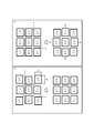
- FIG. 2 is used to explain local differences in substrate expansion and contraction when a planar substrate is bent. It is known that when a flat substrate is bent to form a curved surface, the elongation of the substrate increases in a region closer to the center of the curved surface.
- the setting method of the section 20 for forming the fine structure 2 will be examined.
- square-shaped division groups 20 arranged at equal intervals in the vertical and horizontal directions on the original plane are arranged at equal intervals in the vertical and horizontal directions on the surface of the substrate (silicon wafer 1).
- the partition groups 20 are arranged at unequal intervals in a distribution like barrel distortion in the imaging optical system.
- the square partition groups 20 are arranged in advance on the original flat substrate so as to have an inverse relationship to the barrel distortion. That is, the interval between the sections 20 is set so that the vicinity of the center is narrow and the periphery is wide.
- the partition group 20 is set on the silicon wafer 1 so that a predetermined arrangement (a state in which they are arranged at equal intervals in the vertical and horizontal directions) is obtained after the curved surface forming process is performed.
- FIG. 2 shows a case in which the sections 20 for forming the fine structure 2 are arranged in 3 ⁇ 3 in the vertical direction, but 4 ⁇ 4 in the vertical direction, 3 ⁇ 4 in the vertical direction, and so on. The same applies to other values.
- the groove pattern made of the photoresist can be transferred to the silicon oxide film or the silicon wafer substrate itself by using plasma etching or the like.
- an aluminum film or the like can be deposited on the surface of the microstructure 2 in order to improve optical performance such as reflectance.
- the third step shown in FIG. 1C is a step of thinning the silicon wafer 1 and is one of preparation steps for the curved surface processing.
- the thickness t1 of the silicon wafer 1 is as large as several hundreds of micrometers, it is not suitable for an etching process in a later process. That is, the initial thickness dimension t1 of the silicon wafer 1 is too thick for etching.
- the silicon wafer 1 is thinned by polishing or wet etching from the back surface thereof.
- the thickness dimension t3 of the silicon wafer 1 becomes thinner than the initial value t1 (t3 ⁇ t1).
- the thickness dimension t3 of the silicon wafer 1 after the thinning process is set to a thickness that can maintain rigidity in each section, for example, a thickness of about 100 ⁇ m.
- the 4th process shown in Drawing 1 (d) is a support substrate joining process, and is one of the preparation processes for curved surface formation processing. Since a silicon single crystal is a brittle material, even if it is thinned, if it is curved with a small curvature radius and a large displacement, it will be broken due to a buckling phenomenon or the like.
- the single crystal silicon in the gap 8 partitioning each section is removed by etching so that a large bending displacement can be absorbed by the gap 8 as a “groove”.
- the support substrate 3 made of a flexible material having excellent bendability is bonded to the back surface of the thinned silicon wafer 1, and the position of the microstructure 2 in each separated section is held.
- the support substrate 3 corresponds to a “first substrate”.
- the flexible material for example, nickel is used here, but is not limited thereto.
- Other materials may be used as long as they can be bent uniformly and smoothly by plastic deformation, can maintain the curved shape after plastic deformation, and have rigidity that does not easily deform by external force.
- a metal material rich in spreadability is suitable. It is difficult to maintain a deformed shape of resin and glass with high accuracy.
- resin or glass may be used as the material of the support substrate 3.
- the fifth step shown in FIG. 1 (e) is a gap forming step, which is one of preparation steps for the curved surface forming process.
- the silicon single crystal in the gap 8 is removed by plasma etching or the like.
- the thinned silicon wafer 1 is separated into a single crystal substrate 1A divided into a plurality of sections for each section.
- the separated single crystal substrate 1A corresponds to the “second substrate”.
- the sixth step shown in FIG. 1 (f) is a protective layer forming step.
- the surface of each microstructure 2 is covered with a protective layer 4.
- the thickness unevenness of the protective layer 4 affects the surface accuracy of the curved optical element to be completed. Therefore, the film thickness variation of the protective layer 4 needs to be suppressed to a desired accuracy, for example, 1 ⁇ 4 or less of the wavelength used as the optical element.
- the seventh step shown in FIG. 1 (g) is a curved surface forming step.
- the prepared planar optical element is sandwiched and pressed from both the upper and lower directions.
- the support substrate 3 is plastically deformed to conform to the three-dimensional curved surface shape of the mold.
- the curved surface forming process can also be called a pressurizing process.
- the eighth step shown in FIG. 1 (h) is the final step.
- the optical element 10 having a desired three-dimensional curved surface shape is completed. If the protective layer 4 does not adversely affect the optical properties, it may be left without being removed.
- the fine structure 2 is produced by applying the photolithography technique to the silicon wafer 1. For this reason, according to the present embodiment, it is possible to manufacture a curved optical element having a small size and high accuracy. Further, according to the present embodiment, a pattern with a high degree of freedom can be formed by changing the layout data of the photomask to be used.
- a plurality of small-area sections 20 are set on the surface of the single crystal silicon wafer 1, and the single crystal silicon in the gaps 8 of each section is removed, whereby a plurality of silicon wafers 1 are formed.
- the entire support substrate 3 supporting each single crystal substrate 1A is curved. Therefore, according to the present embodiment, a silicon single crystal which is a brittle material is used, and a curved optical element having a large area as a whole (see element diameter D1 in FIGS. 4 and 5) has a small curvature without causing crystal breakage. It can be formed into a three-dimensional curved surface having a large displacement with a radius.
- the support substrate 3 made of a flexible material can be plastically deformed along the shape of the molds 5 and 6, the surface accuracy of the entire curved optical element is increased. And the accuracy can be maintained.
- the second embodiment will be described with reference to FIG. Since this embodiment corresponds to a modification of the first embodiment, differences from the first embodiment will be mainly described.
- a case will be described in which the present invention is applied to a curved optical element 10A that requires electrical connection, such as a light receiving element, a light emitting element, or a MEMS optical element such as a micromirror or a microshutter.
- the light receiving element array, the light emitting element array, and the MEMS optical element array are array optical elements in which unit elements such as a light receiving element, a light emitting element, and a MEMS element are two-dimensionally arranged. In these array optical elements, it is necessary to electrically connect the unit elements. Therefore, in this embodiment, in the fine structure forming step (FIG. 2B), a unit element is formed as the fine structure 2, and each wiring layer 7 for electrically connecting the single crystal substrates 1A is provided. It is provided between the crystal substrate 1 ⁇ / b> A and the support substrate 3.
- FIG. 2 shows a method of manufacturing the curved optical element 10A according to this example.
- the wafer preparation step (FIG. 1A) which is the first step described in the first embodiment is omitted.
- the second step shown in FIG. 2 (b) is a fine structure forming step in which the fine structure 2 serving as a unit element is formed on the silicon wafer 1 in a predetermined arrangement.
- the third step shown in FIG. 2C is a step of thinning the silicon wafer 1 and is one of the preparation steps for the curved surface processing.
- the 3A process added by the present Example shown in FIG.2 (c2) is a wiring layer formation process in which the wiring layer 7 is formed in the back surface side of the silicon wafer 1 after a thinning process.
- Wiring layer 7 includes a wiring pattern for electrically connecting each single crystal substrate 1A.
- each single crystal substrate 1A is electrically connected to, for example, another single crystal substrate 1A to which each single crystal substrate 1A is to be connected, or a wiring pattern or an electrical element such as a capacitor (not shown). Means that.
- the conductor portion of the wiring layer 7 is formed as a copper foil, and the insulating base portion of the wiring layer 7 is formed of a resin such as polyimide or a rubber material such as silicone.
- the 4th process shown in Drawing 2 (d) is a support substrate joining process, and is one of the preparation processes for curved surface formation processing. In this step, the support substrate 3 is bonded to the back side of the wiring layer 7.
- the fifth step shown in FIG. 2 (e) is a gap forming step, which is one of preparation steps for the curved surface forming process.
- the gap portion 8 is formed by removing the single crystal silicon between the sections by etching.
- the single silicon wafer 1 is divided into single crystal substrates 1A along each section by the gap 8.
- the sixth step shown in FIG. 2 (f) is a protective layer forming step.
- the protective layer 4 is formed so as to cover each single crystal substrate 1A and each gap 8.
- the seventh step shown in FIG. 2 (g) is a curved surface forming step.
- a surface pressure is applied by sandwiching the planar optical element from both sides in the vertical direction by the convex mold 5 and the concave mold 6.
- the single-crystal substrate 1A and the wiring layer 7 divided into the support substrate 3 and the plurality of single-crystal substrates 1A are arranged in a predetermined curved surface shape (a three-dimensional curved surface having a non-developable surface). Shape) to form a curved surface.
- the eighth step shown in FIG. 2 (h) is the final step.
- the molds 5 and 6 are removed, and the protective layer 4 is removed if unnecessary. Thereby, it is possible to obtain an optical element 10A that can transmit and receive electrical signals and has a desired curved surface.
- the wiring layer 7 may be provided inside the supporting substrate 3 or on the back side of the supporting substrate 3 instead of the configuration in which the wiring layer 7 is provided between each single crystal substrate 1A and the supporting substrate 3. In that case, a through electrode for connecting each single crystal substrate 1 ⁇ / b> A and the wiring layer 7 is formed on the support substrate 3.
- This embodiment which is configured in this way, also has the same function and effect as the first embodiment. Further, in this embodiment, since the wiring layer 7 for electrically connecting each single crystal substrate 1A is provided, a unit requiring electrical connection, such as a light receiving element array, a light emitting element array, or a MEMS optical element array. A curved optical element 10A in which elements are arrayed can be obtained.
- the third embodiment will be described with reference to FIG.
- This embodiment relates to an improvement of the first embodiment.
- the base 6 as a “reinforcing member” is joined from the back surface of the support substrate 3 as shown in the cross-sectional view of FIG.
- the mechanical strength of the curved optical element 10B can be increased.
- the lower mold 6 used in the curved surface forming process is used as a pedestal.
- the mold 6 can be bonded to the back side of the support substrate 3 during the curved surface forming step or after the curved surface forming step.
- only the upper mold 5 is removed from the curved optical element in the above-described final step (FIG. 1 (h)).
- the protective layer 4 may be removed or left as it is.
- This embodiment which is configured in this way, also has the same function and effect as the first embodiment. Furthermore, since the base 6 is provided in this embodiment, the strength of the curved optical element 10B can be increased.
- the strength of the curved optical element 10B is increased and the reliability and usability are improved without complicating the manufacturing process. it can.
- a fourth embodiment will be described with reference to FIG. This embodiment relates to an improvement of the second embodiment. Similarly to the third embodiment, in this embodiment, the strength can be secured by joining the base 6 to the curved optical element 10C.
- this invention is not limited to the Example mentioned above.
- a person skilled in the art can make various additions and changes within the scope of the present invention.
- Various numerical values such as the size of the element, the formation density of the parallel grooves, the number of elements arranged, and the width of the gap are examples, and the present invention is not limited thereto.
- An appropriate numerical value may be set according to the use of the element based on the wavelength region to be used.
- the thinning process shown in FIGS. 1C and 2C may be omitted.
- 1 silicon wafer
- 1A single crystal substrate
- 2 fine structure
- 3 support substrate
- 4 protective layer
- 5 upper mold
- 6 lower mold
- 7 wiring layer
- 8 gap
- 10A, 10B, 10C curved surface optical element
Landscapes
- Physics & Mathematics (AREA)
- General Physics & Mathematics (AREA)
- Optics & Photonics (AREA)
- Micromachines (AREA)
Abstract
La présente invention concerne un élément optique à surface incurvée ayant une forme de surface incurvée non-développable dans son ensemble, en utilisant une pluralité de substrats monocristallins. Sur la face supérieure d'un substrat monocristallin unique 1, une pluralité de segments prédéterminés sont définis à des intervalles prédéterminés. Dans chacun des segments prédéterminés, une structure optique prédéterminée 2 est formée (b). Un premier substrat 3 est relié (d) à la face inférieure du substrat monocristallin unique 1 sur lequel sont formées les structures optiques prédéterminées 2. Des rainures 8 s'étendant de la face supérieure du substrat monocristallin unique 1 au premier substrat 3 sont formées dans les intervalles individuels entre les segments prédéterminés, le substrat monocristallin unique 1 étant divisé en segments prédéterminés individuels, et des seconds substrats 1A sont formés (e). En réalisant un procédé de formation de surface incurvée dans lequel le premier substrat 3 et les seconds substrats 1A sont pressés depuis la direction normale, l'une des faces du premier substrat est formée pour avoir une forme de surface incurvée prédéterminée, et la surface d'enveloppe reliant les structures optiques prédéterminées est formée pour avoir une forme de surface incurvée prédéterminée (g).
Priority Applications (1)
| Application Number | Priority Date | Filing Date | Title |
|---|---|---|---|
| PCT/JP2015/050766 WO2016113856A1 (fr) | 2015-01-14 | 2015-01-14 | Élément optique à surface incurvée et son procédé de fabrication |
Applications Claiming Priority (1)
| Application Number | Priority Date | Filing Date | Title |
|---|---|---|---|
| PCT/JP2015/050766 WO2016113856A1 (fr) | 2015-01-14 | 2015-01-14 | Élément optique à surface incurvée et son procédé de fabrication |
Publications (1)
| Publication Number | Publication Date |
|---|---|
| WO2016113856A1 true WO2016113856A1 (fr) | 2016-07-21 |
Family
ID=56405420
Family Applications (1)
| Application Number | Title | Priority Date | Filing Date |
|---|---|---|---|
| PCT/JP2015/050766 Ceased WO2016113856A1 (fr) | 2015-01-14 | 2015-01-14 | Élément optique à surface incurvée et son procédé de fabrication |
Country Status (1)
| Country | Link |
|---|---|
| WO (1) | WO2016113856A1 (fr) |
Citations (6)
| Publication number | Priority date | Publication date | Assignee | Title |
|---|---|---|---|---|
| JP2010079174A (ja) * | 2008-09-29 | 2010-04-08 | Casio Computer Co Ltd | 電気機器 |
| JP2012013530A (ja) * | 2010-06-30 | 2012-01-19 | Fujifilm Corp | 回折格子及びその製造方法、並びに放射線撮影装置 |
| JP2012022239A (ja) * | 2010-07-16 | 2012-02-02 | Fujifilm Corp | 回折格子及びその製造方法、放射線撮影装置 |
| JP2013198661A (ja) * | 2012-03-26 | 2013-10-03 | Konica Minolta Inc | 格子および格子の製造方法ならびに格子ユニットおよび格子ユニットの製造方法 |
| WO2014034033A1 (fr) * | 2012-09-03 | 2014-03-06 | コニカミノルタ株式会社 | Réseau de diffraction et procédé de fabrication de réseau de diffraction, unité réseau et unité de capture d'images rayons x |
| JP2014182301A (ja) * | 2013-03-19 | 2014-09-29 | Hitachi High-Technologies Corp | 曲面回折格子及びその製造方法、並びに光学装置 |
-
2015
- 2015-01-14 WO PCT/JP2015/050766 patent/WO2016113856A1/fr not_active Ceased
Patent Citations (6)
| Publication number | Priority date | Publication date | Assignee | Title |
|---|---|---|---|---|
| JP2010079174A (ja) * | 2008-09-29 | 2010-04-08 | Casio Computer Co Ltd | 電気機器 |
| JP2012013530A (ja) * | 2010-06-30 | 2012-01-19 | Fujifilm Corp | 回折格子及びその製造方法、並びに放射線撮影装置 |
| JP2012022239A (ja) * | 2010-07-16 | 2012-02-02 | Fujifilm Corp | 回折格子及びその製造方法、放射線撮影装置 |
| JP2013198661A (ja) * | 2012-03-26 | 2013-10-03 | Konica Minolta Inc | 格子および格子の製造方法ならびに格子ユニットおよび格子ユニットの製造方法 |
| WO2014034033A1 (fr) * | 2012-09-03 | 2014-03-06 | コニカミノルタ株式会社 | Réseau de diffraction et procédé de fabrication de réseau de diffraction, unité réseau et unité de capture d'images rayons x |
| JP2014182301A (ja) * | 2013-03-19 | 2014-09-29 | Hitachi High-Technologies Corp | 曲面回折格子及びその製造方法、並びに光学装置 |
Similar Documents
| Publication | Publication Date | Title |
|---|---|---|
| CN106716639B (zh) | 使用张力的图像传感器弯曲 | |
| JP4347654B2 (ja) | 可変形状反射鏡及びその製造方法 | |
| CN101606086B (zh) | 用于制备可调透镜的方法 | |
| JP6029502B2 (ja) | 曲面回折格子の製造方法 | |
| TWI430390B (zh) | 減少疊對未對準之直接接合方法 | |
| US20100202071A1 (en) | Deformable mirror | |
| JP2011524084A (ja) | 分子接合を開始する方法 | |
| US8743449B2 (en) | Method and apparatus for providing high-fill-factor micromirror/micromirror arrays with surface mounting capability | |
| JP2001284567A (ja) | オプト・エレクトロニク撮像装置用焦点面および検出器、製造方法およびオプト・エレクトロニク撮像装置 | |
| TW201701450A (zh) | 在具有徑向變化之曲度的模具中彎折半導體晶片 | |
| US20130270662A1 (en) | Image sensor of curved surface | |
| JP2012530370A (ja) | 分子結合による結合方法 | |
| EP2240805B1 (fr) | Eléments optiques suspendus à une membrane, et procédés associés | |
| WO2012126752A1 (fr) | Appareil et procédé de collage direct de tranches, permettant de réduire au minimum une déformation locale | |
| TW201104826A (en) | Mechanical isolation for MEMS electrical contacts | |
| WO2016113856A1 (fr) | Élément optique à surface incurvée et son procédé de fabrication | |
| CN113023661B (zh) | 一种微镜及制作方法 | |
| KR100888080B1 (ko) | 마이크로미러 어레이 제작 방법 | |
| US10437005B2 (en) | Techniques for reducing distortion of optical beam shaping elements | |
| US9676609B2 (en) | Integrated MEMS device | |
| JP2007101649A (ja) | 光学レンズ,および,光学レンズの製造方法 | |
| JP5935396B2 (ja) | Mems素子及びmems素子の製造方法 | |
| US20030197176A1 (en) | Silicon on insulator standoff and method for manufacture thereof | |
| Bifano et al. | Megapixel wavefront correctors | |
| US20250136435A1 (en) | Stretchable electrical interconnect, flexible electronic system, and fabrication method thereof |
Legal Events
| Date | Code | Title | Description |
|---|---|---|---|
| 121 | Ep: the epo has been informed by wipo that ep was designated in this application |
Ref document number: 15877811 Country of ref document: EP Kind code of ref document: A1 |
|
| NENP | Non-entry into the national phase |
Ref country code: DE |
|
| 122 | Ep: pct application non-entry in european phase |
Ref document number: 15877811 Country of ref document: EP Kind code of ref document: A1 |
|
| NENP | Non-entry into the national phase |
Ref country code: JP |