WO2016113858A1 - Moteur et procédé de production de moteur - Google Patents
Moteur et procédé de production de moteur Download PDFInfo
- Publication number
- WO2016113858A1 WO2016113858A1 PCT/JP2015/050779 JP2015050779W WO2016113858A1 WO 2016113858 A1 WO2016113858 A1 WO 2016113858A1 JP 2015050779 W JP2015050779 W JP 2015050779W WO 2016113858 A1 WO2016113858 A1 WO 2016113858A1
- Authority
- WO
- WIPO (PCT)
- Prior art keywords
- substrate
- substrates
- motor
- heat
- board
- Prior art date
- Legal status (The legal status is an assumption and is not a legal conclusion. Google has not performed a legal analysis and makes no representation as to the accuracy of the status listed.)
- Ceased
Links
Images





Classifications
-
- H—ELECTRICITY
- H02—GENERATION; CONVERSION OR DISTRIBUTION OF ELECTRIC POWER
- H02K—DYNAMO-ELECTRIC MACHINES
- H02K11/00—Structural association of dynamo-electric machines with electric components or with devices for shielding, monitoring or protection
Definitions
- the disclosed embodiment relates to a motor and a method for manufacturing the motor.
- Patent Document 1 describes a servo motor with a built-in drive circuit in which a motor drive board and a sensor circuit board are arranged in parallel in a sensor cover.
- the motor drive board and the sensor circuit board are arranged side by side so that the surface direction of the board is perpendicular to the rotation axis direction of the motor. For this reason, there was a problem that the heat of the sensor circuit board disposed on the inner side is likely to be trapped in the sensor cover and the heat dissipation is low.
- the present invention has been made in view of such problems, and an object of the present invention is to provide a motor and a motor manufacturing method capable of improving the heat dissipation of an amplifier unit.
- a motor unit including a stator and a rotor, and a plurality of substrates arranged so that a surface direction is along a rotation axis direction of the motor unit. And an amplifier unit configured to supply electric power to the motor unit.
- a motor manufacturing method including a motor unit including a stator and a rotor, and an amplifier unit configured to supply electric power to the motor unit.
- a method of manufacturing a motor having a plurality of substrates of the amplifier unit inserted into a frame of the amplifier unit along a rotation axis direction of the motor unit is applied.
- a motor unit including a stator and a rotor, an amplifier unit including a plurality of substrates and configured to supply power to the motor unit, and the plurality A motor having a frame that accommodates the substrate and means for dissipating heat of the substrate using at least two opposing surfaces of the frame is applied.
- the heat dissipation of the amplifier section can be improved.
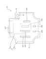
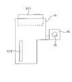
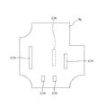
- FIG. 5 is a schematic rear view illustrating a configuration of an amplifier unit as seen through a frame wall. It is a schematic diagram showing a specific example of a board
- FIG. 10 is a schematic rear view illustrating a configuration of a guide member according to a modified example in which a substrate is fitted to a step of the guide member, with a frame wall portion seen through. It is a schematic diagram showing an example of the connection relation of a board
- the motor 1 is an amplifier-integrated motor having an amplifier unit having a motor unit 2, an encoder unit 3, and an amplifier unit 4.
- the motor unit 2 includes a stator and a rotor (both not shown), and is a rotary type (rotary type) motor unit in which the rotor rotates with respect to the stator.
- the motor unit 2 outputs a rotational force by rotating the shaft SH around an axis AX (corresponding to an example of a “rotating shaft”).
- the axial center AX direction is the front-rear direction in this example.
- the rotational output side of the motor unit 2 that is, the side where the shaft SH projects from the motor unit 2 (the front side in this example) is the “load side” and the opposite side (the rear side in this example) is “ It is called “the anti-load side”.
- the motor unit 2 may be a linear type motor unit that includes a stator and a mover, and the mover moves linearly with respect to the stator.
- the encoder unit 3 is connected to the anti-load side (rear side) of the motor unit 2.
- the encoder unit 3 detects the position of the motor unit 2 (also referred to as “rotation position” or “rotation angle”) and outputs position data representing the position.
- the encoder unit 3 may be connected to the load side of the motor unit 2.
- the encoder unit 3 is also referred to as the speed (also referred to as “rotational speed” or “angular velocity”) and acceleration (“rotational acceleration” or “angular acceleration”) of the motor unit 2 in addition to or instead of the position of the motor unit 2. ) May be detected.
- the amplifier unit 4 is connected to the non-load side (rear side) of the encoder unit 3.
- the amplifier unit 4 supplies power to the motor unit 2.
- the amplifier unit 4 acquires position data from the encoder unit 3 and controls the operation of the motor unit 2 by controlling the current or voltage applied to the motor unit 2 based on the position data.
- the amplifier unit 4 acquires a high-order control signal from a high-order control device (not shown), and outputs a rotational force capable of realizing the position and the like represented by the high-order control signal from the shaft SH.
- the operation of the unit 2 can also be controlled.
- the amplifier part 4 may be connected to the anti-load side of the encoder part 3 via another component.
- the amplifier unit 4 may be disposed on the opposite side of the motor unit 2 and on the load side of the encoder unit 3, that is, between the motor unit 2 and the encoder unit 3.
- the amplifier unit 4 may be connected to the load side of the motor unit 2.
- the amplifier unit 4 only needs to be configured to supply power to the motor unit 2, and does not necessarily have to be configured to control the motor unit 2 to follow a target value such as a position.
- the configuration of the motor 1 described above is merely an example, and the configuration of the motor 1 is not limited to the above configuration.
- the encoder unit 3 may be mounted by a device different from the motor 1.
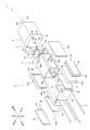
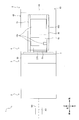
- Example of amplifier configuration> an example of the configuration of the amplifier unit 4 will be described with reference to FIGS. 1 to 8A and 8B. Also, examples of the configuration of the motor unit 2 and the encoder unit 3 will be described as appropriate. In addition, in each figure, illustration of the component of the amplifier part 4 is abbreviate
- the amplifier unit 4 is fixed to the outer surface of the encoder cover 30 included in the encoder unit 3 on the side opposite to the load (rear side) by, for example, four screws S1.
- Screw holes 31 to which the screws S1 are fastened are formed at, for example, the four corners of the rear surface portion of the encoder cover 30. Further, an insertion hole 32 through which a power cable EC1 (described later) is inserted is formed in the vicinity of the lower right corner of the rear surface of the encoder cover 30, for example. Further, a recess 33 into which a head of a screw S2 described later is inserted is formed near the upper right corner of the rear surface of the encoder cover 30, for example. Furthermore, an insertion hole 34 into which a component such as a connector C76 (described later, see FIG. 7) or the like is inserted is formed in the rear surface of the encoder cover 30, for example, in the vicinity of the center.
- a component such as a connector C76 (described later, see FIG. 7) or the like is inserted is formed in the rear surface of the encoder cover 30, for example, in the vicinity of the center.
- the amplifier unit 4 includes a plurality (five in this example) of substrates 5a, 5b, 5c, 5d, and 5e and a backboard 7 (corresponding to an example of “relay substrate”).
- the frame 6 has two guide members 8a and 8b. In FIGS. 1 and 2, the guide members 8a and 8b are not shown.
- the substrates 5 a to 5 e are accommodated in the frame 6.
- the substrates 5a to 5e are arranged side by side so that each surface direction is along the axis AX direction (for example, parallel to the axis AX direction).
- the substrate 5a (corresponding to an example of “first substrate”) is disposed at one end of the substrates 5a to 5e, that is, the right end portion.
- the substrate 5e (corresponding to an example of “second substrate”) is disposed at the other end of the substrates 5a to 5e, that is, at the left end located on the opposite side of the substrate 5a.
- the substrates 5a and 5e correspond to an example of “substrates arranged at end portions of a plurality of substrates”.
- the substrate 5b is disposed adjacent to the left side of the substrate 5a among the substrates 5a to 5e.
- the substrate 5c is disposed adjacent to the left side of the substrate 5b among the substrates 5a to 5e.
- the substrate 5d is disposed adjacent to the left side of the substrate 5c and the right side of the substrate 5e among the substrates 5a to 5e.
- the substrates 5b to 5d arranged at intermediate positions excluding the left and right ends of the substrates 5a to 5e correspond to an example of a “third substrate”.
- the number of the substrates 5 is not limited to five, and may be another number.
- the backboard 7 is disposed on the motor unit 2 side of the frame 6, that is, on the front side so that the surface direction is perpendicular to the axis AX direction.
- the backboard 7 electrically connects the substrates 5b to 5e to constitute a data bus.
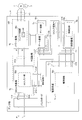
- the amplifier unit 4 converts DC power input from a main power source (not shown) into AC power (three-phase AC power in this example) and supplies the AC power to the motor unit 2.
- the board 5d is a DC input board provided with components constituting the DC input circuit 50d.
- the substrate 5d is appropriately referred to as a “DC input substrate 5d”.
- Two connectors Cd1 and Cd2 are provided on the DC input board 5d (see also FIGS. 1, 2 and 4).
- the DC input circuit 50d inputs DC power from the main power supply.
- the substrate 5a constitutes an inverter circuit 50a (corresponding to an example of “power conversion circuit”) and corresponds to an example of a plurality of switching elements SW (an electronic component that generates heat when energized), which is 1 in FIG. It is a power board provided with components including only one).
- the substrate 5a is appropriately referred to as “power substrate 5a”.
- the power board 5a is provided with a plurality of pin terminals P (see FIGS. 1 and 4).
- the power board 5a is connected to the DC input board 5d via the power cable EC2 and is also connected to the motor unit 2 via the power cable EC1 (see also FIGS. 1 and 4).
- the inverter circuit 50a converts the DC power input from the DC input circuit 50d via the power cable EC2 into three-phase AC power using the switching element SW or the like, and supplies it to the motor unit 2 via the power cable EC1.
- the substrate 5b is a gate substrate provided with components constituting the gate circuit 50b.
- the substrate 5b is appropriately referred to as a “gate substrate 5b”.
- a connector Cb is provided on the gate substrate 5b (see also FIGS. 1 and 4).
- the gate circuit 50b controls the switching element SW of the inverter circuit 50a.
- the power board 5a and its inverter circuit 50a, the gate board 5b and its gate circuit 50b, and the DC input board 5d and its DC input circuit 50d are a main circuit section 500 that supplies three-phase AC power to the motor section 2. Configure.
- the board 5e is a control board provided with components constituting the control circuit 50e.
- the substrate 5e is appropriately referred to as a “control substrate 5e”.
- the control board 5e is provided with a connector Ce (see also FIGS. 1 to 4).
- the control circuit 50e controls the main circuit unit 500. Further, the control circuit 50 e receives position data from the encoder unit 3.
- the substrate 5c is a power supply substrate provided with components constituting the power supply circuit 50c.
- the substrate 5c is appropriately referred to as a “power supply substrate 5c”.
- a connector Cc is provided on the power supply substrate 5c (see also FIGS. 1 and 4).
- the power supply circuit 50c supplies control power to the gate circuit 50b and the control circuit 50e.
- the backboard 7 is provided with a plurality of connectors including connectors C71, C72, C73, C74, and C75 (see also FIGS. 1 to 3).
- the pin terminal P is attached to the gate substrate 5b (see FIGS. 1 and 4). Thereby, the power substrate 5a and the gate substrate 5b are mechanically and electrically connected via the pin terminal P.
- the gate substrate 5b has the connector Cb connected to the connector C71 of the backboard 7
- the power supply substrate 5c has the connector Cc connected to the connector C72 of the backboard 7, and the DC input substrate 5d
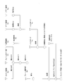
- the connectors Cd1 and Cd2 are connected to the connectors C73 and C74 of the backboard 7, respectively, and the control board 5e is connected to the connector C75 of the backboard 7 (see also FIGS. 1 to 4).
- the gate substrate 5b and the power supply substrate 5c, the gate substrate 5b and the control substrate 5e, the power supply substrate 5c and the control substrate 5e, the DC input substrate 5d and the main power supply, the DC input substrate 5d and the control substrate 5e Is electrically connected.
- the types of the substrates 5a to 5e and the connection relationship between the substrates 5a to 5e and the backboard 7 described above are merely examples, and the types of the substrates 5a to 5e and the connection relationship between the substrates 5a to 5e and the backboard 7 are as follows. The contents other than the above may be used.
- the frame 6 includes a frame housing part 60 having a substantially rectangular parallelepiped shape and two heat radiating plate parts 61 a and 61 b having a heat radiating property, for example, a substantially rectangular plate shape (hereinafter referred to as “heat radiating plate as appropriate”). And a frame cover portion 63 (corresponding to an example of “heat dissipating member” and “substrate fixing member”) having a substantially T-shaped heat dissipation when viewed from above and below.
- the above-mentioned substrates 5a to 5e are accommodated in the frame housing part 60 in parallel. Openings 601, 602, 603, and 604 are formed in the front surface portion, the rear surface portion, the left surface portion, and the right surface portion of the frame housing portion 60, respectively.
- insertion holes 605 through which the screws S1 are inserted are formed through the four corners of the frame housing portion 60 as viewed from the front-rear direction, for example.
- an insertion hole 606 into which a connector C77 described later is inserted is formed in the vicinity of the rear end portion of the upper surface portion of the frame housing portion 60, for example.
- the heat radiating plate portion 61a (corresponding to an example of “first heat radiating plate material”) is detachably attached to the outer surface of the right surface portion of the frame housing portion 60 by, for example, a screw, and constitutes the right wall portion of the frame 6.
- a convex fitting portion 66a that is fitted into the opening 604 of the frame housing portion 60 is formed.
- the power board 5a is disposed in the inner surface of the heat radiating plate portion 61a, specifically, in the vicinity of the front end surface 67a of the fitting portion 66a, and the heat radiating plate portion 61a is heated by the heat substrate 5a to be transferred.
- the heat is dissipated (details will be described later).
- the heat radiating plate portion 61b (corresponding to an example of “second heat radiating plate material”) is detachably attached to the outer surface of the left surface portion of the frame housing portion 60 by, for example, screws, and constitutes the left wall portion of the frame 6.
- a convex fitting portion 66b that fits into the opening 603 of the frame housing portion 60 is formed on the inner surface of the heat radiating plate portion 61b.
- the control board 5e is disposed on the inner surface of the heat radiating plate portion 61b, specifically, in the vicinity of the front end surface 67b of the fitting portion 66b, and the heat radiating plate portion 61b is heated by the heat transferred from the control board 5e.
- the heat is dissipated (details will be described later).
- the frame cover part 63 is attached to the outer surface of the rear surface part located on the opposite side to the motor part 2 of the frame housing part 60.
- the frame cover part 63 includes, for example, a substantially rectangular plate-like frame wall part 64 and an extending part 65.
- the insertion holes 641 through which the screws S1 are inserted are formed through, for example, the four corners of the frame wall 64.
- Each screw S ⁇ b> 1 is inserted from the outer surface side of the frame wall portion 64 into the insertion hole 641 of the frame wall portion 64 and the insertion hole 605 of the frame housing portion 60, and is fastened to the screw hole 31 of the encoder cover 30.
- the frame housing part 60 is fixed to the outer surface of the rear surface part of the encoder cover 30, and the frame wall part 64 is fixed to the outer surface of the rear surface part of the frame housing part 60, and Configure the wall.
- the extending portion 65 extends from the inner surface of the frame wall portion 64 in the frame housing portion 60 along the axial center AX direction (for example, parallel to the axial center AX direction).
- the substrates 5a to 5e are fixed to the extending portion 65 in a state where they are arranged side by side. Specifically, between the power board 5a and the gate board 5b, between the gate board 5b and the power board 5c, between the power board 5c and the DC input board 5d, and between the DC input board 5d and the control board 5e.
- resin pallets Pa1, Pa2, Pa3, Pa4, which serve as spacers are arranged. In FIGS. 1, 3, and 4, the pallets Pa1 to Pa4 are not shown.
- the substrates 5a to 5e are fixed to the extending portion 65 in a state where they are stacked via pallets Pa1 to Pa4.
- the power supply board 5c and the DC input board 5d are disposed in the vicinity of the extending part 65, and the frame cover part 63 radiates the heat of the power supply board 5c and the DC input board 5d to be transferred (details will be described later). .
- the heat radiating plate portions 61a and 61b and the frame cover portion 63 correspond to an example of “means for radiating heat of the substrate using at least two opposing surfaces of the frame”.
- the configuration of the frame 6 described above is merely an example, and the configuration of the frame 6 may be other than the above as long as it can accommodate the substrates 5a to 5e.
- one or both of the heat radiating plate portions 61a and 61b may be detachable from the frame housing portion 60 (including a case where the heat radiating plate portions 61a and 61b are integrated with the frame housing portion 60).
- the frame 6 may include only one of the heat radiating plate portions 61a and 61b. Or the flame
- frame cover part 63 thermally radiates is not limited to both board
- the frame cover portion 63 may radiate the heat of the substrate 5b in addition to or instead of the substrates 5c and 5d. Further, the frame cover portion 63 may include a plurality of extending portions to which the substrate 5 is fixed.
- the guide members 8 a and 8 b are fixed inside the frame housing portion 60. Specifically, the guide members 8a and 8b are fixed at corresponding positions on the inner surface of the upper surface portion and the inner surface of the lower surface portion of the frame housing portion 60, respectively.
- Grooves 81, 82, 83, and 84 are provided along the axis AX direction at a plurality of (four in this example) positions corresponding to the opposing surfaces of the guide members 8a and 8b ( For example, it is formed in parallel with the axis AX direction.
- the groove 81 is formed at the right end of the opposing surface of the guide members 8a and 8b.
- the groove 82 is formed with a predetermined distance on the left side of the groove 81 on the opposed surfaces of the guide members 8a and 8b.
- the groove 83 is formed with a predetermined distance on the left side of the groove 82 on the opposing surfaces of the guide members 8a and 8b.
- the groove 84 is formed at a left side of the groove 83 on the opposing surface of the guide members 8a and 8b, that is, at the left end portion of the opposing surface of the guide members 8a and 8b.
- the grooves 81 and 81, the grooves 82 and 82, the grooves 83 and 83, and the grooves 84 and 84 of the guide members 8a and 8b are respectively provided at the upper and lower ends of the gate substrate 5b, the upper and lower ends of the power supply substrate 5c, and the DC input substrate 5d.
- the upper and lower ends and the upper and lower ends of the control board 5e are fitted. In this way, by fixing the gate substrate 5b, the power supply substrate 5c, the DC input substrate 5d, and the control substrate 5e, they can be fixed without using screws.
- the configuration of the guide members 8a and 8b described above is merely an example, and the guide member is not limited to the above as long as the recess into which the substrate 5 is fitted is formed along the axis AX direction. It may be configured as follows.
- the recess formed in the guide member and into which the substrate 5 is fitted is not limited to a groove (slit), but may be a recess having another shape (for example, a step).
- the number and shape of the guide members are not limited to the above number and shape, and may be other numbers and shapes.
- a plurality of substrates 5 may be fixed in the frame 6 without using a guide member. At this time, a plurality of recesses (for example, grooves and steps) are formed on the inner surface of the frame 6 along the axis AX direction. Then, a plurality of substrates 5 may be fitted into the plurality of recesses.
- the power substrate 5a has the pin terminal P attached to the gate substrate 5b and is disposed in the vicinity of the front end surface 67a of the heat radiating plate portion 61a.
- the plurality of switching elements SW which are electronic components having a relatively large amount of heat generation are arranged.
- a heat conductive sheet having heat conductivity.
- thermo conduction member 9a (corresponding to an example of “thermal conduction member”) is arranged. 2 and 3, the illustration of the heat conductive sheet 9a is omitted.
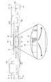
- the power substrate 5a is in contact with the front end surface 67a of the heat radiating plate portion 61a through the heat conductive sheet 9a, and the heat radiating plate portion 61a transfers the heat of the power substrate 5a that is transferred through the heat conductive sheet 9a. Dissipate heat.
- the power board 5a is a double-sided board, and components are arranged on the left surface 51 and the right surface 52, respectively.
- the power board 5a On the left surface 51 of the power board 5a, there are a switch board 53 on which the switching element SW is mounted, and a part 10a2 having a relatively large dimension in the thickness direction of the power board 5a (hereinafter referred to as “high-back part 10a2” as appropriate). Has been placed. That is, the power board 5a and the heat radiating plate portion 61a are disposed on the same direction side (right side) with respect to the switching element SW.
- the switching element SW is mounted on the power substrate 5a as it is without an IC chip enclosed in the package. That is, the switching element SW is bare-chip mounted on the power substrate 5a.
- the switch substrate 53 is made of a material having high thermal conductivity such as ceramic.
- the switch substrate 53 is provided with a bonding wire W for supplying power to the switching element SW.
- the switch substrate 53, the switching element SW, the bonding wire W, the tall component 10a2, and the like disposed on the left surface 51 side of the power substrate 5a are sealed with a resin 59.
- a part 10a1 having a relatively small dimension in the thickness direction of the power board 5a, specifically, smaller than the thermal conductive sheet 9a (hereinafter referred to as “low-profile part 10a1” as appropriate). Is arranged.
- the low-profile component 10a1 is disposed in a region other than the region corresponding to the switch substrate 53 on the right surface 52 of the power substrate 5a, and is covered with the heat conductive sheet 9a.
- a plurality of thermal vias 54 are formed in a region corresponding to the switch substrate 53 of the power substrate 5a.
- the thermal via 54 is configured by filling a through hole 55 formed in the power substrate 5a with a thermally conductive material 56 having thermal conductivity such as copper (see a partially enlarged view in FIG. 6). ).
- the thermal via 54 forming portion of the power substrate 5a has a smaller thermal resistance in the thickness direction of the power substrate 5a than the other portions.
- the heat conductive sheet 9a is located between the front end surface 67a of the heat radiating plate portion 61a and the right surface 52 of the power board 5a.
- the region of the right surface 52 corresponds to at least the switch board 53 (in this example, the right surface 52). It is arranged so as to be in contact with substantially the entire area. Therefore, the heat of the switching element SW is transferred to the heat radiating plate portion 61a through the switch substrate 53, the power substrate 5a, and the heat conductive sheet 9a, and is radiated by the heat radiating plate portion 61a.
- the heat conductive sheet 9a is a resin sheet having anisotropy in heat conductivity.
- the heat conductive sheet 9a has anisotropy in which the thermal conductivity in the plane direction is higher than that in the thickness direction by adjusting the orientation of the filler to be added.
- the heat of the switching element SW is diffused in the surface direction from the corresponding region of the switch substrate 53 (see the thick arrow shown in the partially enlarged view in FIG. 6), and efficiently. Heat can be transferred to the radiator plate 61a.
- fins or the like may be provided on the outer surface of the heat radiating plate portion 61a.
- the thermal via 54 and the heat conductive sheet 9a correspond to an example of “means for transferring heat of electronic components to the frame via the first substrate”.
- substrate 5a demonstrated above is an example to the last, and the heat dissipation of the power board 5a may be ensured by structures other than the above.
- the power board 5a is made of a material having high thermal conductivity such as ceramic, or a metal plate is formed inside the power board 5a (metal core). ) Or pasting together (metal base).
- the IC chip of the switching element SW is bare-chip mounted, but the IC chip of the switching element SW may be a surface-mount package product such as a QFN product. Further, the IC chip package constituting the switching element SW may be configured such that the heat radiating surface and the terminal surface are in the same direction. In this case, the size of the package can be reduced.
- the control board 5e has both upper and lower ends fitted into the grooves 84 and 84 of the guide members 8a and 8b, and in the vicinity of the front end surface 67b of the heat radiating plate 61b. Is arranged.
- a plurality of electronic components 10e having a smaller amount of heat generation than the switching element SW are arranged.
- a heat conductive sheet 9d having thermal conductivity (corresponding to an example of “heat conductive member”) is disposed.
- the thermal conductive sheet 9d is a resin sheet having anisotropy in thermal conductivity, similar to the thermal conductive sheet 9a.
- the electronic component 10e of the control board 5e is in contact with the front end surface 67b of the heat radiating plate portion 61b through the heat conductive sheet 9d, and the heat radiating plate portion 61b is an electronic component that is transferred through the heat conductive sheet 9d.
- the heat of 10e is dissipated.
- the gate substrate 5b is fixed to the power substrate 5a via the pin terminal P, and both upper and lower end portions are fitted into the grooves 81 and 81 of the guide members 8a and 8b, and are arranged in the vicinity of the power substrate 5a. Yes.
- On the left surface of the gate substrate 5b opposite to the power substrate 5a for example, an electronic component 10b that generates a small amount of heat is disposed.
- the electronic component 10b and the like of the gate substrate 5b are sealed with resin (not shown).
- the upper and lower ends of the power supply substrate 5c are fitted into the grooves 82 and 82 of the guide members 8a and 8b, and are arranged in the vicinity of the right surface of the extending portion 65 of the frame cover portion 63.
- an electronic component 10c having a smaller amount of heat generation than the switching element SW is disposed.
- a heat conductive sheet 9b having thermal conductivity is disposed between the right surface of the extending portion 65 and the left surface of the power supply substrate 5c.
- illustration of the heat conductive sheet 9b is abbreviate
- the heat conductive sheet 9b is a resin sheet having anisotropy in heat conductivity, like the heat conductive sheet 9a.
- the electronic component 10c of the power supply substrate 5c is in contact with the right surface of the extending portion 65 through the heat conductive sheet 9b.
- the upper and lower ends of the DC input board 5d are fitted in the grooves 83 and 83 of the guide members 8a and 8b, and are arranged in the vicinity of the left surface of the extending portion 65 of the frame cover portion 63.
- an electronic component 10d having a calorific value smaller than that of the switching element SW is disposed.
- a thermally conductive sheet 9c having thermal conductivity is disposed between the left surface of the extending portion 65 and the right surface of the DC input board 5d.
- the thermal conductive sheet 9c is a resin sheet having anisotropy in thermal conductivity, similar to the thermal conductive sheet 9a.
- the electronic component 10d on the right surface side of the DC input board 5d is in contact with the left surface of the extending portion 65 via the heat conductive sheet 9c.
- heat of the electronic components 10c and 10d of the power supply substrate 5c and the DC input substrate 5d is transferred to the extending portion 65 through the heat conductive sheets 9b and 9c.
- the frame cover part 63 (frame wall part 64) radiates the heat of the electronic components 10c and 10d transferred through the heat conductive sheets 9b and 9c.
- the above-described configuration for enhancing the heat dissipation of the substrates 5a to 5e is merely an example, and the substrates 5a to 5e may have a heat dissipation property other than those described above.
- the substrates 5a to 5e may have a heat dissipation property other than those described above.
- the heat conductive sheets 9a to 9d instead of part or all of the heat conductive sheets 9a to 9d, other heat conductive members may be used.
- the amplifier unit 4 may not include some or all of the heat conductive sheets 9a to 9d.
- the backboard 7 includes a plurality (two in this example) of backboards 7 a and 7 b (corresponding to an example of “relay board”) integrated with a resin 321. By being sealed, it is unitized and configured as a substrate unit 70. In FIG. 1 and FIGS. 3 to 5, a single substrate-like backboard 7 is schematically illustrated instead of the substrate unit 70.
- the substrate unit 70 is attached to the opening 601 of the frame casing 60 and is fixed to the front surface of the frame casing 60 by, for example, one screw S2.
- the backboards 7a and 7b are arranged in parallel in the direction of the axis AX so that the backboard 7a is the rear side and the backboard 7b is the front side.
- the connector C73 is provided on the rear surface of the backboard 7a. Further, a connector C77 connected to the main power source is provided on, for example, the front surface of the backboard 7a. That is, a high voltage system power line is arranged on the backboard 7a, and the backboard 7a constitutes a power system backboard.
- the connectors C71, C72, C74, C75 are provided on the rear surface of the backboard 7b.
- a connector C76 connected to the encoder unit 3 is provided on the front surface of the backboard 7b. That is, a low voltage system signal line is arranged on the backboard 7b, and the backboard 7b constitutes a backboard of the control system.
- the back board 7a is provided with a fixed piece 72 having an insertion hole 73 through which the screw S2 is inserted.
- the screw S ⁇ b> 2 is inserted into the insertion hole 73 of the back board 7 a from the front side of the board unit 70 and is fastened to the front surface portion of the frame housing unit 60.
- the substrate unit 70 is attached to the opening 601 of the frame casing 60 and fixed to the front surface of the frame casing 60.
- the connector C77 is inserted into the insertion hole 606 of the frame housing part 60.
- the parts such as the connector C76 and the head of the screw S2 are inserted into the insertion hole 34 and the recess 33 of the encoder cover 30, respectively.
- the configuration of the backboard 7 described above is merely an example, and the backboard 7 has a configuration other than the above as long as at least one of the substrates 5a to 5e can be electrically connected. Also good.
- the backboard 7 is constituted by a plurality of backboards, but the plurality of backboards may not be integrally sealed with the resin 71.
- the backboard 7 may be constituted by a single backboard.
- the substrates 5a to 5e may be electrically connected without using the back board 7 (for example, by a cable or a connector).
- the manufacturing process (assembly process) of the motor 1 by the manufacturing method of the motor 1 before the main process is executed (or in parallel with the main process), the power substrate 5a and the gate substrate 5b
- the connecting process and the manufacturing process of the substrate unit 70 are executed.
- the switch substrate 53, the switching element SW, the bonding wire W, the high-profile component 10a2, etc. of the power substrate 5a are sealed with the resin 59.
- the electronic component 10b and the like of the gate substrate 5b are sealed with resin.
- the pin terminal P of the power substrate 5a is attached to the gate substrate 5b in a state where the pallet Pa1 is interposed between the resin-sealed power substrate 5a and the resin-sealed gate substrate 5b. Are connected (joined). Thereby, a combined body of the power substrate 5a and the gate substrate 5b is completed.
- the backboards 7a and 7b are connected (joined) by, for example, solder or the like and then integrally sealed with the resin 71. Thereby, the substrate unit 70 is completed.
- the power supply substrate 5c is assembled to the extending portion 65 of the frame cover portion 63 via the heat conductive sheet 9b.
- the DC input board 5d is assembled to the extending portion 65 of the frame cover portion 63 via the heat conductive sheet 9c and the pallet Pa3.
- the control board 5e is assembled via the pallet Pa4 on the DC input board 5d side in the extending portion 65 of the frame cover part 63 to which the power supply board 5c and the DC input board 5d are fixed.
- the power board 5c and the gate board 5b are connected to the power board 5c side of the extending part 65 of the frame cover part 63 to which the power board 5c, the DC input board 5d, and the control board 5e are fixed via the pallet Pa2.
- the gate substrate 5b side in the combined body is assembled. As described above, the substrates 5a to 5e are fixed to the extended portion 65 of the frame cover portion 63 in a state where they are arranged side by side.
- the extending portion 65 of the frame cover portion 63 and the substrates 5a to 5e fixed to the extending portion 65 are inserted into the frame housing portion 60 from the opening portion 602 along the axial center AX direction.
- the extending portion 65 and the substrates 5a to 5e are such that the upper and lower ends of the gate substrate 5b, the power supply substrate 5c, the DC input substrate 5d, and the control substrate 5e are the guide members 8a and 8b in the frame housing portion 60. Are inserted into the grooves 81 to 84, respectively.
- the connectors on the backboards 7a and 7b are connected to the corresponding connectors on the gate board 5b, the power supply board 5c, the DC input board 5d, and the control board 5e in the frame housing section 60. In addition, it is assembled to the opening 601 of the frame housing part 60.
- the heat radiating plate portion 61a is arranged so that the front end surface 67a of the fitting portion 66a is in contact with the power substrate 5a in the frame housing portion 60 via the heat conductive sheet 9a.
- the frame housing portion 61b is arranged so that the front end surface 67b of the fitting portion 66b is brought into contact with the electronic component 10e of the control board 5e in the frame housing portion 60 through the heat conductive sheet 9d.
- 60 is assembled to the outer surface (opening portion 603) of the left surface portion. Thereby, the amplifier unit 4 is completed.
- the amplifier unit 4 is assembled to the outer surface of the encoder cover 30 on the side opposite to the load of the encoder cover 30. Thereby, the motor 1 having the motor unit 2, the encoder unit 3, and the amplifier unit 4 is completed.
- the manufacturing process of the motor 1 by the manufacturing method of the motor 1 demonstrated above is an example to the last, and the manufacturing process of the motor 1 is not necessarily a process performed in time series along the order demonstrated above. A process that is not executed in time series but executed in parallel or individually is also included. Even in the process executed in time series, the order can be appropriately changed depending on circumstances.
- the power board 5a is inserted into the frame housing part 60 in a state of being fixed to the extension part 65 of the frame cover part 63. However, the power board 5a is assembled to the heat radiating plate part 61a via the heat conductive sheet 9a. May be inserted into the frame housing part 60.
- the motor 1 of this embodiment is an amplifier-integrated motor including the motor unit 2 and the amplifier unit 4.
- the substrates 5 a to 5 e of the amplifier unit 4 are arranged so that their surface directions are perpendicular to the axial center AX direction, they are arranged at the end opposite to the motor unit 2.
- the heat dissipation is good for the substrate 5, the heat dissipation is low for the other substrates 5 arranged on the inside, and heat tends to be trapped in the amplifier section 4.
- the influence on the heat radiation area when the motor 1 is reduced in the radial direction is large, the reduction in size may be restricted in terms of heat dissipation.
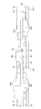
- the substrates 5a to 5e of the amplifier unit 4 are arranged so that their surface directions are along the axis AX direction. That is, when the motor 1 is assembled, the substrates 5a to 5e of the amplifier unit 4 are inserted into the frame housing unit 60 along the axis AX direction, so that the substrates 5a to 5e are obtained in the amplifier unit 4 of the assembled motor 1. Are arranged side by side so that their surface directions are along the direction of the axis AX. Thereby, since heat dissipation can be improved about the board
- the frame 6 includes a heat radiating plate portion 61a that radiates heat from the power board 5a and a heat radiating plate portion 61b that radiates heat from the control board 5e.
- substrates 5a and 5e can be conducted to the flame
- the following effects can be obtained. That is, a plurality of electronic components are mounted on the component surfaces of the substrates 5a and 5e. At this time, unevenness occurs on the component surfaces of the substrates 5a and 5e due to the difference in height between the electronic components. Therefore, by providing the heat conductive sheets 9a and 9d between the power board 5a and the heat radiating plate portion 61a and between the control board 5e and the heat radiating plate portion 61b, the unevenness caused by the electronic components is absorbed, and the substrate 5a, The thermal contact area between the electronic component 5e and the heat radiating plate portions 61a and 61b can be increased. Therefore, the heat dissipation of the substrates 5a and 5e can be improved.
- heat conductive sheets 9a and 9d having anisotropy in heat conduction as the heat conductive members, heat from the substrates 5a and 5e to the heat radiating plate portions 61a and 61b is obtained. It is possible to increase the conductivity and further improve the heat dissipation.
- the following effects can be obtained. That is, if the heat radiating plate portions 61a and 61b and the frame housing portion 60 are integrated, the power substrate 5a and the heat radiating plate portion are structured so that the substrates 5a and 5e are inserted into and removed from the frame 6 in the axis AX direction. It is necessary to provide a gap between the control board 5e and the heat radiating plate portion 61b, and there is a possibility that the thermal contact area between the substrates 5a and 5e and the heat radiating plate portions 61a and 61b may be reduced. is there.
- the heat radiating plate portions 61a and 61b are detachable from the frame housing portion 60, the heat radiating plate portions 61a and 61b are attached to the frame after the substrates 5a and 5e are accommodated in the frame housing portion 60. It can be attached to the housing part 60. Thereby, it becomes possible to ensure the thermal contact area of board
- the frame cover portion 63 radiates heat from the substrates 5c and 5d.
- the heat of the substrates 5c and 5d arranged at the intermediate positions excluding both ends is difficult to dissipate and easily stays in the amplifier unit 4.
- the heat of the substrates 5c and 5d can be radiated to the opposite side of the motor unit 2 through the frame cover unit 63, so that the heat dissipation of the amplifier unit 4 can be further improved.
- the substrates 5a to 5e are fixed to the frame cover portion 63 in a state where they are arranged side by side. Thereby, the fixing structure of the substrates 5a to 5e can be made firm. Further, when the motor 1 is assembled, the board 5a to 5e can be attached at a time by attaching the frame cover 63 to the amplifier unit 4 from the opposite side of the motor 2, so that the motor 1 can be assembled. It can be simplified. Further, when the substrates 5a to 5e are fixed to the frame cover 63, the necessary distance between the substrates (insulation distance) is ensured by stacking the substrates 5a to 5e via the resin pallets Pa1 to Pa4. It becomes possible. Further, when the substrates 5a to 5e are fixed to the frame cover portion 63, it is possible to facilitate the subsequent assembling work by performing necessary connector connection between the substrates in advance.
- the frame cover portion 63 includes a frame wall portion 64 constituting a wall portion of the frame 6 opposite to the motor portion 2, and an axial center from the frame wall portion 64 in the frame housing portion 60. And an extending portion 65 extending along the AX direction to which the substrates 5a to 5e are fixed.
- the frame wall part 64 which is a part of the flame
- the backboard 7 is used to connect the substrates 5b to 5e. Thereby, wiring saving in the amplifier part 4 is attained.
- the backboard 7 has a configuration in which the backboards 7 a and 7 b arranged in parallel in the axial center AX direction are integrally sealed with the resin 71.
- the backboard 7 can be separated into a power system backboard and a control system backboard.
- the backboards 7a and 7b can be unitized by integrally resin-sealing, and the assembly workability can be improved.
- the amplifier section 4 is disposed inside the frame housing section 60, and guide members in which grooves 81 to 84 into which the substrates 5b to 5e are fitted are formed along the axis AX direction. 8a and 8b.
- the grooves 81 to 84 of the guide members 8a and 8b the substrates 5b to 5e are guided in the direction of the axis AX when the substrates 5a to 5e are inserted into and removed from the frame housing portion 60. It becomes easy. Further, since the intervals between the substrates 5b to 5e can be fixed (positioned) by the grooves 81 to 84 of the guide members 8a and 8b, a necessary distance between the substrates (insulation distance) can be ensured.
- the substrates 5a to 5e include the power substrate 5a provided with the switching elements SW that are disposed at the ends of the substrates 5a to 5e and constitute the inverter circuit 50a.
- the heat dissipation of the power board 5a with a comparatively large calorific value can be secured.
- the substrates 5a to 5e include a control substrate 5e that is disposed at the end of the substrates 5a to 5e opposite to the power substrate 5a and includes a control circuit 50e.
- the influence of noise can be reduced by separating the control board 5e from the power board 5a.
- the heat dissipation of the control board 5e heat from the CPU, ASIC, etc. can be secured.
- the configuration of the comparative example is shown in FIG.
- the switch substrate 53 on which the switching element SW is mounted is attached to the heat sink 100 (corresponding to “the heat radiating plate portion 61 a of the present embodiment”) via the base B having thermal conductivity. Yes.
- the IC chip of the switching element SW is enclosed in a package 57.
- the switch board 53 is connected to the power board 5 a located on the opposite side of the heat sink 100 by a pin terminal 58.
- the power substrate 5a and the heat radiating plate 61a are arranged on the same direction side with respect to the switching element SW.
- the switching element SW can be reduced in size.
- a useless space corresponding to the height of the switching element SW is required between the heat sink 100 and the power substrate 5a.
- the heat conductive sheet 9a is disposed between the heat radiating plate portion 61a and the power substrate 5a and the switching element SW is not disposed, the useless space can be reduced.
- the amplifier unit 4 can be reduced in size.
- region corresponding to at least switching element SW of the right surface 52 of the power board 5a is arrange
- a thermal via 54 in which the heat conductive material 56 is filled in the through hole 55 is formed in a region corresponding to the switching element SW of the power substrate 5a.
- the thermal conductive sheet 9a a resin sheet having anisotropy in thermal conductivity is used as the thermal conductive sheet 9a.
- the heat conductive sheet 9a which is a resin sheet having anisotropy whose surface direction thermal conductivity is higher than the thickness direction as in this embodiment. It is possible to diffuse heat in the surface direction from the region corresponding to the switching element SW and to transfer heat to the heat radiating plate 61a more efficiently. Therefore, the heat dissipation of the amplifier unit 4 can be further enhanced. Further, by using the resin thermal conductive sheet 9a, it is possible to secure insulation between the power substrate 5a and the heat radiating plate portion 61a, and to reduce the amount of solder used since the number of metal bonds can be reduced.
- the low-profile component 10a1 in which the dimension in the thickness direction of the power substrate 5a is smaller than that of the heat conductive sheet 9a is disposed on the right surface 52 of the power substrate 5a. Accordingly, the low-profile component 10a1 disposed on the right surface 52 is covered with the heat conductive sheet 9a, so that the thermal contact area between the heat conductive sheet 9a and the front end surface 67a of the heat radiating plate portion 61a. The heat dissipation of the amplifier unit 4 can be further enhanced.
- a low-profile component 10a1 having a relatively small size in the thickness direction of the power substrate 5a is disposed on the right surface 52 of the power substrate 5a, and a high-profile component 10a2 having a relatively large size is disposed on the left surface 51 together with the switching element SW.
- the power board 5a can be disposed close to the tip end surface 67a of the heat radiating plate portion 61a. Therefore, further downsizing can be realized.
- the switch board 53 on which the switching element SW is mounted is disposed on the left surface 51 of the power board 5a.
- the heat conductive sheet 9a is arrange
- the heat of the switching element SW can be efficiently transferred from the switch board 53 to the heat radiating plate 61a through the power board 5a.
- the heat dissipation can be further enhanced by configuring the switch substrate 53 with a material having high thermal conductivity such as ceramic as in the present embodiment.
- the heat radiating plate portion 61a ′ (corresponding to an example of “first heat radiating plate portion”) of the present modified example protrudes from the distal end surface 67a ′ of the fitting portion 66a ′ toward the power board 5a.
- Convex portion 610 (corresponding to an example of “heat conducting member”) is provided.
- the convex portion 610 corresponds to the switch substrate 53 of the right surface 52 between the tip surface 67a ′ of the heat radiating plate portion 61a ′ and the right surface 52 of the power board 5a, instead of the above-described heat conductive sheet 9a. It arrange
- the heat radiating plate portion 61a ′, the above-described heat radiating plate portion 61b, and the above-described frame cover portion 63 are examples of “means for radiating the heat of the substrate using at least two opposing surfaces of the frame”. It corresponds to. Further, the thermal via 54 and the convex portion 610 described above correspond to an example of “means for transferring the heat of the electronic component to the frame via the first substrate”.
- the same effect as the above embodiment can be obtained.
- the heat of the switching element SW is efficiently transferred from the power board 5a to the heat sink 61a 'by the convex part 610 protruding toward the power board 5a from the tip surface 67a' of the heat sink 61a '. Can heat. Further, since it is not necessary to make the heat conduction member easy, parts can be reduced and the configuration can be simplified.
- guide members 8c and 8d are fixed inside the frame housing portion 60.
- the guide members 8c and 8d are fixed to corresponding positions on the right inner surface and the left inner surface of the frame housing part 60, respectively.
- a groove 801 along the axial center AX direction is formed in the vicinity of the central portion in the vertical direction on the right surface of the guide member 8c.
- an electronic component 10b and a connector Cb disposed on the left surface of the gate substrate 5b, a tip portion of the pin terminal P protruding to the left side of the gate substrate 5b, and the like are disposed.
- steps 85 and 85 are along the axis AX direction (for example, parallel to the axis AX direction). Is formed.
- the gate substrate 5b is fitted to the steps 85, 85.
- a groove 802 along the axis AX direction is formed in the vicinity of the central portion in the vertical direction on the left surface of the guide member 8c. Further, at both upper and lower edges of the groove 801 on the left surface of the guide member 8c, steps 86 and 86 (corresponding to an example of “concave part”) are along the axis AX direction (for example, parallel to the axis AX direction). Is formed.
- the power supply board 5c is fitted to the steps 86, 86.
- a groove 803 along the axis AX direction is formed in the vicinity of the central portion in the vertical direction on the right surface of the guide member 8d.
- an electronic component 10d or the like disposed on the left surface of the DC input board 5d is disposed.
- steps 87 and 87 are along the axis AX direction (for example, parallel to the axis AX direction). Is formed.
- the DC input board 5d is fitted to the steps 87, 87.
- a groove 804 along the axis AX direction is formed in the vicinity of the central portion in the vertical direction on the left surface of the guide member 8d.
- a connector Ce disposed on the right surface of the control board 5e is disposed.
- steps 88 and 88 are along the axis AX direction (for example, parallel to the axis AX direction). Is formed.
- the control board 5e is fitted to the steps 88, 88.
- the same effect as the above embodiment can be obtained. That is, according to the present modification, when the substrates 5a to 5e are inserted into and removed from the frame housing portion 60, the substrates 5b to 5e are guided in the direction of the axis AX by the steps 85 to 88 of the guide members 8c and 8d. In addition, it is easy to insert and remove the substrates 5a to 5e. Further, since the distance between the substrates 5b to 5e can be fixed by the steps 85 to 88 of the guide members 8c and 8d, a necessary distance between the substrates can be ensured.
- the DC input board 5d is provided with three connectors Cd1, Cd2, and Cd3.
- the power board 5a is connected to the DC input board 5d via the power cable EC2 and is connected to the motor unit 2 via the power cable EC1.
- the power board 5a is provided with a connector Ca.
- Three connectors Cb, Cc2, and Cb3 are provided on the gate substrate 5b.
- a connector Ce is provided on the control board 5e.
- the power supply board 5c is provided with three connectors Cc, Cc2, and Cc3.
- the backboard 7 'of this modification is provided with a plurality of connectors including connectors C71, C72, C73, C74, C75.
- the power substrate 5a and the gate substrate 5b are mechanically and electrically connected to each other through the pin terminal P described above, as in the above embodiment.
- the gate substrate 5b has the connector Cb connected to the connector C71 of the backboard 7 '
- the power supply substrate 5c has the connector Cc connected to the connector C72 of the backboard 7'.
- the connectors Cd1 and Cd2 are respectively connected to the connectors C73 and C74 of the backboard 7 '
- the control board 5e has the connector Ce connected to the connector C75 of the backboard 7'.
- the encoder unit 3 described above is electrically connected to the backboard 7 '.
- the gate board 5b and the control board 5e, the power board 5c and the control board 5e, the DC input board 5d and the main power source, the DC input board 5d and the control board 5e, the encoder unit 3 and the control board 5e are respectively connected to the back board 7 '. It is electrically connected via.
- the power board 5a has the connector Ca connected to the connector Cb2 of the gate board 5b
- the gate board 5b has the connector Cb3 connected to the connector Cc2 of the power board 5c
- the power board 5c The connector Cc3 is connected to the connector Cd3 of the DC input board 5d.
- the power board 5a and the gate board 5b, the gate board 5b and the power board 5c, the power board 5c and the DC input board 5d are directly electrically connected by the connectors Ca and Cb2, the connectors Cb3 and Cc2, and the connectors Cc3 and Cd3, respectively. It is connected to the.
- the connectors Ca, Cb2, Cb3, Cc2, Cc3, and Cd3 correspond to an example of “a connector that electrically connects a plurality of substrates”.
- connection relationship between the substrates 5a to 5e and the backboard 7 'described above is merely an example, and the connection relationship between the substrates 5a to 5e and the backboard 7' may be other than the above.
- the gate board 5b and the control board 5e, the power board 5c and the control board 5e, the DC input board 5d and the main power source, the DC input board 5d and the control board 5e, the encoder unit 3 and the control board 5e are respectively connected to the backboard.
- electrically connected via 7 ' a part or all of these may be directly electrically connected by a connector.
- the power board 5a and the gate board 5b, the gate board 5b and the power board 5c, the power board 5c and the DC input board 5d are directly connected to the connectors Ca and Cb2, the connectors Cb3 and Cc2, and the connectors Cc3 and Cd3, respectively. Although electrically connected, some or all of these may be electrically connected via the backboard.
- the same effect as the above embodiment can be obtained.
- the connectors Ca and Cb2 are used for direct connection between the boards 5a and 5b
- the connectors Cb3 and Cc2 are used for direct connection between the boards 5b and 5c
- the connectors Cc3 and Cd3 are used. Direct connection is made between the substrates 5c and 5d. Thereby, further wiring saving in the amplifier unit 4 is possible.
Landscapes
- Engineering & Computer Science (AREA)
- Power Engineering (AREA)
- Motor Or Generator Cooling System (AREA)
- Cooling Or The Like Of Electrical Apparatus (AREA)
Abstract
L'objectif de la présente invention est d'améliorer des propriétés de dissipation de chaleur d'une unité d'amplificateur. A cette fin, le moteur (1) selon l'invention comprend : une unité de moteur (2) équipée d'un stator et d'un rotor; et une unité d'amplificateur (4) qui comporte des substrats (5a-5e) respectivement placés de telle sorte que la direction de la surface se trouve le long de la direction de l'axe (AX) de l'unité de moteur (2), et qui fournit de l'énergie à l'unité de moteur (2). En outre, l'unité d'amplificateur (4) comprend un châssis (6) destiné à recevoir les substrats (5a-5e). Le châssis (6) présente : une partie de plaque de dissipation de chaleur (61a) conçue pour dissiper la chaleur du substrat d'alimentation (5a) parmi les substrats (5a-5e), disposée au niveau d'une extrémité; et une partie de plaque de dissipation de chaleur (61b) conçue pour dissiper la chaleur du substrat de commande (5e) parmi les substrats (5a-5e), disposée au niveau d'une autre extrémité.
Priority Applications (3)
| Application Number | Priority Date | Filing Date | Title |
|---|---|---|---|
| PCT/JP2015/050779 WO2016113858A1 (fr) | 2015-01-14 | 2015-01-14 | Moteur et procédé de production de moteur |
| PCT/JP2015/068695 WO2016113929A1 (fr) | 2015-01-14 | 2015-06-29 | Moteur et procédé de production de moteur |
| JP2015561454A JP5991605B1 (ja) | 2015-01-14 | 2015-06-29 | モータ及びモータの製造方法 |
Applications Claiming Priority (1)
| Application Number | Priority Date | Filing Date | Title |
|---|---|---|---|
| PCT/JP2015/050779 WO2016113858A1 (fr) | 2015-01-14 | 2015-01-14 | Moteur et procédé de production de moteur |
Publications (1)
| Publication Number | Publication Date |
|---|---|
| WO2016113858A1 true WO2016113858A1 (fr) | 2016-07-21 |
Family
ID=56405422
Family Applications (2)
| Application Number | Title | Priority Date | Filing Date |
|---|---|---|---|
| PCT/JP2015/050779 Ceased WO2016113858A1 (fr) | 2015-01-14 | 2015-01-14 | Moteur et procédé de production de moteur |
| PCT/JP2015/068695 Ceased WO2016113929A1 (fr) | 2015-01-14 | 2015-06-29 | Moteur et procédé de production de moteur |
Family Applications After (1)
| Application Number | Title | Priority Date | Filing Date |
|---|---|---|---|
| PCT/JP2015/068695 Ceased WO2016113929A1 (fr) | 2015-01-14 | 2015-06-29 | Moteur et procédé de production de moteur |
Country Status (2)
| Country | Link |
|---|---|
| JP (1) | JP5991605B1 (fr) |
| WO (2) | WO2016113858A1 (fr) |
Cited By (1)
| Publication number | Priority date | Publication date | Assignee | Title |
|---|---|---|---|---|
| WO2019077647A1 (fr) * | 2017-10-16 | 2019-04-25 | 三菱電機株式会社 | Appareil de direction à assistance électrique |
Families Citing this family (2)
| Publication number | Priority date | Publication date | Assignee | Title |
|---|---|---|---|---|
| CN110140284B (zh) * | 2016-12-28 | 2022-06-28 | 日本电产株式会社 | 马达和电动助力转向装置 |
| DE102021133952A1 (de) | 2021-12-21 | 2023-06-22 | Synapticon GmbH | Motorvorrichtung mit einer multifunktionalen Zwischeneinheit, die zwischen einer Motoreinheit und einer Servoantriebseinheit der Motorvorrichtung angeordnet ist |
Citations (7)
| Publication number | Priority date | Publication date | Assignee | Title |
|---|---|---|---|---|
| JPH02266854A (ja) * | 1989-04-04 | 1990-10-31 | Honda Motor Co Ltd | エンジンの始動・発電装置 |
| JPH0630547A (ja) * | 1991-12-20 | 1994-02-04 | Gold Star Co Ltd | インバータ一体型電動機 |
| JPH11313465A (ja) * | 1998-04-28 | 1999-11-09 | Toshiba Corp | 制御装置付きモータ |
| JP2004282905A (ja) * | 2003-03-17 | 2004-10-07 | Hitachi Ltd | 多相式交流回転電機 |
| JP2011163232A (ja) * | 2010-02-10 | 2011-08-25 | Mitsubishi Heavy Ind Ltd | インバータ一体型電動圧縮機およびその組立方法 |
| JP2012092747A (ja) * | 2010-10-27 | 2012-05-17 | Mitsubishi Heavy Ind Ltd | インバータ一体型電動圧縮機 |
| JP2012180828A (ja) * | 2011-02-07 | 2012-09-20 | Aisan Industry Co Ltd | 電動ポンプ |
Family Cites Families (2)
| Publication number | Priority date | Publication date | Assignee | Title |
|---|---|---|---|---|
| JP2000217310A (ja) * | 1999-01-22 | 2000-08-04 | Harmonic Drive Syst Ind Co Ltd | ドライバ―一体型モ―タ |
| JP5020212B2 (ja) * | 2008-10-14 | 2012-09-05 | 株式会社キーエンス | スピードコントローラ |
-
2015
- 2015-01-14 WO PCT/JP2015/050779 patent/WO2016113858A1/fr not_active Ceased
- 2015-06-29 JP JP2015561454A patent/JP5991605B1/ja not_active Expired - Fee Related
- 2015-06-29 WO PCT/JP2015/068695 patent/WO2016113929A1/fr not_active Ceased
Patent Citations (7)
| Publication number | Priority date | Publication date | Assignee | Title |
|---|---|---|---|---|
| JPH02266854A (ja) * | 1989-04-04 | 1990-10-31 | Honda Motor Co Ltd | エンジンの始動・発電装置 |
| JPH0630547A (ja) * | 1991-12-20 | 1994-02-04 | Gold Star Co Ltd | インバータ一体型電動機 |
| JPH11313465A (ja) * | 1998-04-28 | 1999-11-09 | Toshiba Corp | 制御装置付きモータ |
| JP2004282905A (ja) * | 2003-03-17 | 2004-10-07 | Hitachi Ltd | 多相式交流回転電機 |
| JP2011163232A (ja) * | 2010-02-10 | 2011-08-25 | Mitsubishi Heavy Ind Ltd | インバータ一体型電動圧縮機およびその組立方法 |
| JP2012092747A (ja) * | 2010-10-27 | 2012-05-17 | Mitsubishi Heavy Ind Ltd | インバータ一体型電動圧縮機 |
| JP2012180828A (ja) * | 2011-02-07 | 2012-09-20 | Aisan Industry Co Ltd | 電動ポンプ |
Cited By (2)
| Publication number | Priority date | Publication date | Assignee | Title |
|---|---|---|---|---|
| WO2019077647A1 (fr) * | 2017-10-16 | 2019-04-25 | 三菱電機株式会社 | Appareil de direction à assistance électrique |
| JPWO2019077647A1 (ja) * | 2017-10-16 | 2020-04-02 | 三菱電機株式会社 | 電動パワーステアリング装置 |
Also Published As
| Publication number | Publication date |
|---|---|
| JPWO2016113929A1 (ja) | 2017-04-27 |
| JP5991605B1 (ja) | 2016-09-14 |
| WO2016113929A1 (fr) | 2016-07-21 |
Similar Documents
| Publication | Publication Date | Title |
|---|---|---|
| JP6573013B2 (ja) | 電子部品搭載用放熱基板 | |
| KR101748639B1 (ko) | 전력 변환 장치 | |
| JP6501022B2 (ja) | 電子部品搭載用放熱基板 | |
| JP6020379B2 (ja) | 半導体装置 | |
| CN107403774A (zh) | 半导体装置和马达装置 | |
| JP6245379B2 (ja) | モータ及びモータの製造方法 | |
| JP5991605B1 (ja) | モータ及びモータの製造方法 | |
| JP6021047B1 (ja) | モータ |
Legal Events
| Date | Code | Title | Description |
|---|---|---|---|
| 121 | Ep: the epo has been informed by wipo that ep was designated in this application |
Ref document number: 15877812 Country of ref document: EP Kind code of ref document: A1 |
|
| NENP | Non-entry into the national phase |
Ref country code: DE |
|
| 122 | Ep: pct application non-entry in european phase |
Ref document number: 15877812 Country of ref document: EP Kind code of ref document: A1 |
|
| NENP | Non-entry into the national phase |
Ref country code: JP |