WO2016121577A1 - Procédé de production de cristal - Google Patents
Procédé de production de cristal Download PDFInfo
- Publication number
- WO2016121577A1 WO2016121577A1 PCT/JP2016/051449 JP2016051449W WO2016121577A1 WO 2016121577 A1 WO2016121577 A1 WO 2016121577A1 JP 2016051449 W JP2016051449 W JP 2016051449W WO 2016121577 A1 WO2016121577 A1 WO 2016121577A1
- Authority
- WO
- WIPO (PCT)
- Prior art keywords
- temperature
- crystal
- solution
- crucible
- seed crystal
- Prior art date
- Legal status (The legal status is an assumption and is not a legal conclusion. Google has not performed a legal analysis and makes no representation as to the accuracy of the status listed.)
- Ceased
Links
Images



Classifications
-
- C—CHEMISTRY; METALLURGY
- C30—CRYSTAL GROWTH
- C30B—SINGLE-CRYSTAL GROWTH; UNIDIRECTIONAL SOLIDIFICATION OF EUTECTIC MATERIAL OR UNIDIRECTIONAL DEMIXING OF EUTECTOID MATERIAL; REFINING BY ZONE-MELTING OF MATERIAL; PRODUCTION OF A HOMOGENEOUS POLYCRYSTALLINE MATERIAL WITH DEFINED STRUCTURE; SINGLE CRYSTALS OR HOMOGENEOUS POLYCRYSTALLINE MATERIAL WITH DEFINED STRUCTURE; AFTER-TREATMENT OF SINGLE CRYSTALS OR A HOMOGENEOUS POLYCRYSTALLINE MATERIAL WITH DEFINED STRUCTURE; APPARATUS THEREFOR
- C30B15/00—Single-crystal growth by pulling from a melt, e.g. Czochralski method
- C30B15/14—Heating of the melt or the crystallised materials
-
- C—CHEMISTRY; METALLURGY
- C30—CRYSTAL GROWTH
- C30B—SINGLE-CRYSTAL GROWTH; UNIDIRECTIONAL SOLIDIFICATION OF EUTECTIC MATERIAL OR UNIDIRECTIONAL DEMIXING OF EUTECTOID MATERIAL; REFINING BY ZONE-MELTING OF MATERIAL; PRODUCTION OF A HOMOGENEOUS POLYCRYSTALLINE MATERIAL WITH DEFINED STRUCTURE; SINGLE CRYSTALS OR HOMOGENEOUS POLYCRYSTALLINE MATERIAL WITH DEFINED STRUCTURE; AFTER-TREATMENT OF SINGLE CRYSTALS OR A HOMOGENEOUS POLYCRYSTALLINE MATERIAL WITH DEFINED STRUCTURE; APPARATUS THEREFOR
- C30B15/00—Single-crystal growth by pulling from a melt, e.g. Czochralski method
- C30B15/20—Controlling or regulating
-
- C—CHEMISTRY; METALLURGY
- C30—CRYSTAL GROWTH
- C30B—SINGLE-CRYSTAL GROWTH; UNIDIRECTIONAL SOLIDIFICATION OF EUTECTIC MATERIAL OR UNIDIRECTIONAL DEMIXING OF EUTECTOID MATERIAL; REFINING BY ZONE-MELTING OF MATERIAL; PRODUCTION OF A HOMOGENEOUS POLYCRYSTALLINE MATERIAL WITH DEFINED STRUCTURE; SINGLE CRYSTALS OR HOMOGENEOUS POLYCRYSTALLINE MATERIAL WITH DEFINED STRUCTURE; AFTER-TREATMENT OF SINGLE CRYSTALS OR A HOMOGENEOUS POLYCRYSTALLINE MATERIAL WITH DEFINED STRUCTURE; APPARATUS THEREFOR
- C30B19/00—Liquid-phase epitaxial-layer growth
- C30B19/02—Liquid-phase epitaxial-layer growth using molten solvents, e.g. flux
- C30B19/04—Liquid-phase epitaxial-layer growth using molten solvents, e.g. flux the solvent being a component of the crystal composition
-
- C—CHEMISTRY; METALLURGY
- C30—CRYSTAL GROWTH
- C30B—SINGLE-CRYSTAL GROWTH; UNIDIRECTIONAL SOLIDIFICATION OF EUTECTIC MATERIAL OR UNIDIRECTIONAL DEMIXING OF EUTECTOID MATERIAL; REFINING BY ZONE-MELTING OF MATERIAL; PRODUCTION OF A HOMOGENEOUS POLYCRYSTALLINE MATERIAL WITH DEFINED STRUCTURE; SINGLE CRYSTALS OR HOMOGENEOUS POLYCRYSTALLINE MATERIAL WITH DEFINED STRUCTURE; AFTER-TREATMENT OF SINGLE CRYSTALS OR A HOMOGENEOUS POLYCRYSTALLINE MATERIAL WITH DEFINED STRUCTURE; APPARATUS THEREFOR
- C30B19/00—Liquid-phase epitaxial-layer growth
- C30B19/08—Heating of the reaction chamber or the substrate
-
- C—CHEMISTRY; METALLURGY
- C30—CRYSTAL GROWTH
- C30B—SINGLE-CRYSTAL GROWTH; UNIDIRECTIONAL SOLIDIFICATION OF EUTECTIC MATERIAL OR UNIDIRECTIONAL DEMIXING OF EUTECTOID MATERIAL; REFINING BY ZONE-MELTING OF MATERIAL; PRODUCTION OF A HOMOGENEOUS POLYCRYSTALLINE MATERIAL WITH DEFINED STRUCTURE; SINGLE CRYSTALS OR HOMOGENEOUS POLYCRYSTALLINE MATERIAL WITH DEFINED STRUCTURE; AFTER-TREATMENT OF SINGLE CRYSTALS OR A HOMOGENEOUS POLYCRYSTALLINE MATERIAL WITH DEFINED STRUCTURE; APPARATUS THEREFOR
- C30B29/00—Single crystals or homogeneous polycrystalline material with defined structure characterised by the material or by their shape
- C30B29/10—Inorganic compounds or compositions
- C30B29/36—Carbides
Definitions
- the present invention relates to a method for producing a silicon carbide crystal.
- silicon carbide which is a compound of carbon and silicon
- SiC silicon carbide
- SiC has attracted attention because of its wide band gap compared to silicon and high electric field strength that leads to dielectric breakdown.
- Japanese Patent Application Laid-Open No. 2012-136391 describes manufacturing a silicon carbide crystal wafer, and thus a silicon carbide crystal ingot.
- the method for producing a crystal of the present disclosure is a method for producing a crystal of silicon carbide, and includes a preparation step, a contact step, a first growth step, a temperature raising step, a temperature lowering step, and a second growth step.
- the preparation step includes a step of preparing a seed crystal, a crucible, and a solution obtained by dissolving carbon in a silicon solvent stored in the crucible.
- the contacting step includes a step of bringing the lower surface of the seed crystal into contact with the solution.
- the temperature of the solution is raised to a first temperature range, and the seed crystal is pulled up while maintaining the temperature of the solution in the first temperature range, thereby growing a crystal on the lower surface of the seed crystal. Process.
- FIG. 1 shows an outline of a crystal manufacturing apparatus. It should be noted that the present disclosure is not limited to the embodiment (this embodiment), and various changes and improvements can be made without departing from the gist of the present invention.
- the crystal manufacturing apparatus 1 is an apparatus for manufacturing a silicon carbide crystal 2 used for semiconductor parts and the like.
- the crystal manufacturing apparatus 1 manufactures the crystal 2 by growing the crystal 2 on the lower surface of the seed crystal 3.
- the crystal manufacturing apparatus 1 mainly includes a holding member 4 and a crucible 5.
- the seed crystal 3 is fixed to the holding member 4, and the solution 6 is accommodated in the crucible 5.
- the crystal manufacturing apparatus 1 causes the lower surface of the seed crystal 3 to contact the solution 6 to grow the crystal 2 on the lower surface of the seed crystal 3.
- Crystal 2 is processed into a wafer, for example, and this wafer becomes a part of the semiconductor component through a semiconductor component manufacturing process.
- Crystal 2 is a lump of silicon carbide crystals grown on the lower surface of seed crystal 3.
- the crystal 2 may be, for example, a plate shape or a column shape having, for example, a circular shape or a polygonal planar shape when viewed in cross section.
- the crystal 2 may be, for example, a silicon carbide single crystal.
- the diameter or width of the crystal 2 can be set to, for example, 25 mm or more and 200 mm or less.
- the height of the crystal 2 can be set to 30 mm or more and 300 mm or less, for example.
- the “diameter or width” refers to the length of a straight line that reaches the edge through the center of the planar shape of the crystal 2.
- the height of the crystal 2 refers to the distance from the lower surface of the crystal 2 to the upper surface (the lower surface of the seed crystal 3).
- the seed crystal 3 can be a seed of the crystal 2 grown by the crystal manufacturing apparatus 1. In other words, the seed crystal 3 becomes a base for the crystal 2 to grow.
- the seed crystal 3 may be, for example, a flat plate having a circular or polygonal planar shape.
- the seed crystal 3 may be a crystal made of the same material as the crystal 2.
- a seed crystal 3 made of a silicon carbide crystal is used to manufacture the silicon carbide crystal 2.
- the seed crystal 3 is made of a single crystal or polycrystal. In the present embodiment, the seed crystal 3 is a single crystal.
- the seed crystal 3 is fixed to the lower surface of the holding member 4.
- the seed crystal 3 is fixed to the holding member 4 with, for example, an adhesive containing carbon.
- the holding member 4 can hold the seed crystal 3.
- the holding member 4 carries the seed crystal 3 in and out of the solution 6. In other words, the holding member 4 can bring the seed crystal 3 into contact with the solution 6 or keep the crystal 2 away from the solution 6.
- the holding member 4 is fixed to the moving mechanism of the moving device 7 as shown in FIG.
- the moving device 7 can move the holding member 4 in the vertical direction using, for example, a motor.
- the holding member 4 is moved in the vertical direction by the moving device 7, and the seed crystal 3 can be moved in the vertical direction as the holding member 4 is moved.
- the holding member 4 may have a columnar shape, for example.
- the holding member 4 may be, for example, a carbon polycrystal or a fired body obtained by firing carbon.
- the holding member 4 may be fixed to the moving device 7 so as to be rotatable around an axis extending in the vertical direction through the center of the planar shape of the holding member 4. In other words, the holding member 4 may be capable of rotating.
- the solution 6 is accumulated (contained) inside the crucible 5, and the raw material of the crystal 2 can be supplied to the seed crystal 3 in order to grow the crystal 2.
- Solution 6 contains the same material as crystal 2. That is, since the crystal 2 is a silicon carbide crystal, the solution 6 contains carbon and silicon.
- the solution 6 of this embodiment is obtained by dissolving carbon as a solute in a silicon solvent (silicon solvent).
- the solution 6 is made of, for example, neodymium (Nd), aluminum (Al), tantalum (Ta), scandium (Sc), chromium (Cr), zirconium (Zr), nickel for the purpose of improving the solubility of carbon.
- One or more metal materials such as (Ni) or yttrium (Y) may be included as an additive.
- the crucible 5 can store the solution 6.
- the crucible 5 can melt the raw material of the crystal 2 inside.
- the crucible 5 may be formed of a material containing carbon, for example.
- the crucible 5 of the present embodiment is made of, for example, graphite.
- the solution 6 is obtained by melting silicon in the crucible 5 and dissolving a part (carbon) of the crucible 5 in the melted silicon.
- the crucible 5 is, for example, a concave member opened on the upper surface in order to store the solution 6.
- a solution method is used as a method for growing the silicon carbide crystal 2.
- the solution 6 is controlled in such a manner that the precipitation of the crystal 2 proceeds more than the elution while keeping the thermodynamically metastable state in the vicinity of the seed crystal 3, and the crystal 2 is grown on the lower surface of the seed crystal 3.
- carbon (solute) is dissolved in silicon (solvent), and the solubility of carbon increases as the temperature of the solvent increases.
- the solution 6 heated to a high temperature is cooled by contact with the seed crystal 3, the dissolved carbon becomes supersaturated, and the solution 6 is locally metastable in the vicinity of the seed crystal 3. .
- the solution 6 is deposited as a silicon carbide crystal 2 on the lower surface of the seed crystal 3 in an attempt to shift to a stable state (thermodynamic equilibrium state).
- the crystal 2 can be grown on the lower surface of the seed crystal 3.
- the crucible 5 is arranged inside the crucible container 8.
- the crucible container 8 can hold the crucible 5.
- a heat insulating material 9 is disposed between the crucible container 8 and the crucible 5. This heat insulating material 9 surrounds the periphery of the crucible 5. The heat insulating material 9 can suppress the heat radiation from the crucible 5 and make the temperature distribution in the crucible 5 close to uniform.
- the crucible 5 may be disposed inside the crucible container 8 so as to be rotatable around an axis extending in the vertical direction through the center of the bottom surface of the crucible 5. In other words, the crucible 5 may be capable of rotating.
- the crucible container 8 is arranged inside the chamber 10.
- the chamber 10 can separate the space in which the crystal 2 is grown from the external atmosphere. By having the chamber 10, it is possible to reduce mixing of extra impurities in the crystal 2.
- the atmosphere inside the chamber 10 may be filled with, for example, an inert gas. Thereby, the inside of the chamber 10 can be shut off from the outside.
- the crucible container 8 may be supported by the bottom surface of the chamber 10, but may be supported by a support shaft that extends downward from the bottom surface of the crucible container 8 through the bottom of the chamber 10.
- the chamber 10 has a passage hole 101 through which the holding member 4 passes, an air supply hole 102 for supplying gas into the chamber 10, and an exhaust hole 103 for discharging gas from the chamber 10. Furthermore, the crystal manufacturing apparatus 1 has a gas supply unit that supplies gas into the chamber 10. The gas in the atmosphere of the crystal manufacturing apparatus 1 is supplied from the air supply hole 102 into the chamber 10 through the gas supply unit, and is discharged from the exhaust hole 103.
- the chamber 10 may be cylindrical, for example.
- the chamber 10 has a circular bottom surface with a diameter of 150 mm to 1000 mm, for example, and has a height of 500 mm to 2000 mm, for example.
- the chamber 10 may be formed of a material such as stainless steel or insulating quartz, for example.
- the inert gas supplied into the chamber 10 may be, for example, argon (Ar) or helium (He).
- the heating device 11 of the present embodiment includes a coil 12 and an AC power source 13, and can heat the crucible 5 by, for example, an electromagnetic heating method using electromagnetic waves.
- the heating device 11 may employ other methods such as a method of transferring heat generated by a heating resistor such as carbon.
- a heating resistor is disposed (between the crucible 5 and the heat insulating material 9).
- the coil 12 is formed of a conductor and surrounds the periphery of the crucible 5. Specifically, the coil 12 is disposed around the chamber 10 so as to surround the crucible 5 in a cylindrical shape.
- the heating device 11 having the coil 12 has a cylindrical heating region formed by the coil 12. In the present embodiment, the coil 12 is disposed around the chamber 10, but the coil 12 may be positioned inside the chamber 10.
- the AC power supply 13 can pass an AC current through the coil 12.
- an electric current flows through the coil 12 and an electric field is generated, an induced current is generated in the crucible container 8 located in the electric field.
- the crucible container 8 is heated by the Joule heat of the induced current. And the heat
- the frequency of the alternating current so that the induced current easily flows through the crucible container 8, the heating time to the set temperature in the crucible 5 can be shortened, and the power efficiency can be improved.
- the AC power supply 13 and the moving device 7 are connected to the control device 14 and controlled. That is, in the crystal manufacturing apparatus 1, the heating and temperature control of the solution 6 and the loading / unloading of the seed crystal 3 are controlled by the control device 14 in conjunction with each other.
- the control device 14 includes a central processing unit and a storage device such as a memory, and is composed of, for example, a known computer.
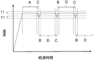
- FIG. 2 is a diagram for explaining a method for producing a crystal according to the present disclosure. Specifically, an outline of a temperature change of the solution 6 during crystal production when the elapsed time is on the horizontal axis and the temperature is on the vertical axis. It is a graph which shows.
- the crystal manufacturing method mainly includes a preparation step, a first growth step, a temperature raising step, a temperature lowering step, a second growth step, and a separation step. It should be noted that the present disclosure is not limited to the embodiments, and various changes and improvements can be made without departing from the scope of the present invention.
- a seed crystal 3 is prepared.
- the seed crystal 3 may be formed, for example, by forming a silicon carbide crystal lump produced by a sublimation method or a solution method into a flat plate shape.
- the crystal 2 obtained by the crystal manufacturing method of the present disclosure is used as the seed crystal 3.
- the composition of the seed crystal 3 and the crystal 2 grown on the surface of the seed crystal 3 can be brought close to each other, and the occurrence of transition due to the difference in composition in the crystal 2 can be reduced.
- what is necessary is just to perform the process to flat form by cutting the lump of silicon carbide by machining, for example.
- the holding member 4 is prepared, and the seed crystal 3 is fixed to the lower surface of the holding member 4. Specifically, after preparing the holding member 4, an adhesive containing carbon is applied to the lower surface of the holding member 4. Next, the seed crystal 3 is arranged on the lower surface of the holding member 4 with the adhesive interposed therebetween, and the seed crystal 3 is fixed to the lower surface of the holding member 4. In this embodiment, after fixing the seed crystal 3 to the holding member 4, the upper end of the holding member 4 is fixed to the moving device 7. As described above, the holding member 4 is rotatably fixed to the moving device 7 around an axis extending through the central portion of the holding member 4 and extending in the vertical direction.
- a crucible 5 and a solution 6 contained in the crucible 5 in which carbon is dissolved in a silicon solvent are prepared. Specifically, first, the crucible 5 is prepared. Next, silicon particles as a raw material of silicon are placed in the crucible 5 and the crucible 5 is heated to a melting point of silicon (1420 ° C.) or higher. At this time, carbon (solute) forming the crucible 5 is dissolved in silicon (solvent) melted and liquefied. As a result, a solution 6 in which carbon is dissolved in a silicon solvent can be prepared in the crucible 5. In order to include carbon in the solution 6, carbon particles may be dissolved at the same time as the silicon particles are melted by adding carbon particles as a raw material in advance.
- the crucible 5 is accommodated in the chamber 10.
- the crucible 5 is disposed and accommodated in the crucible container 8 via the heat insulating material 9 in the chamber 10 surrounded by the coil 12 of the heating device 11.
- the preparation of the solution 6 may be performed by housing the crucible 5 in the chamber 10 and heating the crucible 5 with the heating device 11.
- the crucible 5 may be stored in the chamber 10 after the crucible 5 is heated outside the crystal production apparatus 1 to form the solution 6 in advance.
- the solution 6 may be poured into the crucible 5 installed in the chamber 10.
- the lower surface of the seed crystal 3 is brought into contact with the solution 6.
- the seed crystal 3 brings the lower surface into contact with the solution 6 by moving the holding member 4 downward.
- the seed crystal 3 is brought into contact with the solution 6 by moving the seed crystal 3 downward.
- the lower surface of the seed crystal 3 is moved to the solution 6 by moving the crucible 5 upward. You may make it contact.
- the seed crystal 3 only needs to have at least the lower surface of the seed crystal 3 in contact with the liquid surface of the solution 6.
- the seed crystal 3 may be submerged in the solution 6, and the side surface or the upper surface of the seed crystal 3 may be brought into contact with the solution 6 together with the lower surface.
- the crystal 2 is grown from the solution 6 on the lower surface of the seed crystal 3 brought into contact with the solution 6.
- the crystal 2 first, there is a temperature difference between the lower surface of the seed crystal 3 and the solution 6 near the lower surface of the seed crystal 3. If the carbon dissolved in the solution 6 becomes supersaturated due to the temperature difference between the seed crystal 3 and the solution 6, the carbon and silicon in the solution 6 become silicon carbide crystals 2 on the lower surface of the seed crystal 3. Precipitates and crystal 2 grows.
- the crystal 2 only needs to grow at least on the lower surface of the seed crystal 3, but may grow from the lower surface and side surfaces of the seed crystal 3.
- the crystal 2 By pulling up the seed crystal 3, the crystal 2 can be grown in a columnar shape. That is, the crystal 2 can be grown while maintaining a certain width or diameter by gradually pulling the seed crystal 3 upward while adjusting the growth rate of the crystal 2 in the planar direction and downward.
- the pulling speed of the seed crystal 3 can be set to, for example, 50 ⁇ m / h or more and 2000 ⁇ m / h or less.
- the seed crystal 3 is pulled up while raising the solution 6 to the first temperature range and maintaining the temperature of the solution 6 in the first temperature range T1. That is, the crystal 2 is grown while controlling the temperature of the solution 6 to be constant.
- the temperature control of the solution 6 becomes easier and the working efficiency can be improved as compared with the case where the temperature of the solution 6 is changed.
- the first growth step is “A”
- the temperature raising step is “B”
- the second growth step is “D”.
- FIGS. 3 and 4 various processes are indicated by alphabets as in FIG. 1.
- the first temperature range T1 refers to a temperature range within ⁇ 10 ° C. with respect to the temperature of the solution 6 when the crystal 2 is grown. Further, in the first growth step, the temperature of the solution 6 during the growth of the crystal 2 can be set, for example, within a range from 1900 ° C. to 2100 ° C. In the first growth step, the growth time of the crystal 2 can be set to, for example, 10 hours or more and 150 hours or less.
- a method of measuring the temperature of the solution 6 for example, a method of directly measuring with a thermocouple or a method of measuring indirectly with a radiation thermometer can be used.
- a temperature obtained by averaging temperatures measured a plurality of times in a certain time can be used.
- the temperature of the solution 6 may be raised to the first temperature range T1 after contacting the seed crystal 3 with the solution 6. According to this, for example, the surface of the seed crystal 3 can be dissolved by the solution 6, and dust or the like adhering to the surface of the seed crystal 3 can be removed. As a result, the quality of the crystal 2 growing on the surface of the seed crystal 3 can be improved.
- the temperature of the solution 6 may be raised to the first temperature range T1 before the seed crystal 3 contacts the solution 6.
- dissolution of the seed crystal 3 can be reduced before the first crystal growth step, and the production efficiency of the crystal 2 can be improved.
- the temperature increase range of the temperature of the solution 6 can be set to 30 ° C. or more and 200 ° C. or less, for example.
- the temperature of the solution 6 can be raised to a second temperature region T2 higher than the first temperature region T1.
- the second temperature range T2 can be set to 1930 ° C. or higher and 2300 ° C. or lower, for example.
- the temperature raising step is performed after the temperature lowering step described later, the temperature of the solution 6 can be raised to the first temperature range T1.
- the temperature of the solution 6 can be adjusted, for example, by changing the output of the heating device 11.
- the temperature raising step can be performed, for example, by spending 0.5 hours to 3 hours.
- the temperature raising step may be performed by separating the crystal 2 grown in the first growth step from the solution 6. As a result, melting of the crystal 2 can be reduced, and the production efficiency of the crystal 2 can be improved.
- the temperature raising step may be performed by bringing the crystal 2 into contact with the solution 6.
- the surface of the crystal 2 can be dissolved by the solution 6.
- the groove of the crystal 2 can be eliminated.
- the crystal 2 may be separated from the solution 6 during the temperature raising step. As a result, the amount for dissolving the crystal 2 can be adjusted.
- the crystal 2 When the crystal 2 is separated from the solution 6, the crystal 2 may be rotated. As a result, the amount of the solution 6 adhering to the lower surface of the crystal 2 can be reduced.
- a silicon raw material may be added to the solution 6 in the temperature raising step. Thereby, silicon consumed by crystal growth or evaporation can be replenished, and the composition of the solution 6 can be easily maintained at a desired composition. As a result, the quality of the crystal 2 can be improved.
- a silicon raw material may be added before the temperature raising step. As a result, carbon can be sufficiently dissolved in the temperature raising step, so that the subsequent second growth step can be easily started.
- the nitrogen concentration in the solution 6 is reduced by the temperature raising process. If nitrogen is not supplied, the nitrogen concentration of the solution 6 can be reduced. As a result, for example, the crystal 2 having a reduced nitrogen concentration can be manufactured by a subsequent second growth step.
- the amount of dopant in the crystal 2 grown in the subsequent second growth step can be adjusted by performing the temperature raising step and the temperature lowering step after the first growth step. Further, by adjusting the dopant amount as described above, for example, a striped pattern can be formed on the crystal 2 and can be used as a mark when the crystal 2 is processed into a wafer.
- the temperature lowering process may be performed after the temperature increasing process.
- the temperature of the solution 6 can be raised to the second temperature range T2, bubbles generated in the solution 6 during expansion can be expanded, and discharged out of the solution 6 by buoyancy.
- the temperature raising step may be performed after the temperature lowering step.
- the maximum temperature of the solution 6 becomes the first temperature range T1
- the safety measures of the apparatus and the capacity of the heater power source can be reduced, and the power required for production can also be reduced.
- the deterioration of the quality of the crystal 2 can be reduced by not giving an extra temperature history to the crystal 2.
- the temperature drop width of the temperature of the solution 6 can be set to 30 ° C. or more and 200 ° C. or less, for example.
- the temperature of the solution 6 can be raised to a third temperature region T3 that is lower than the first temperature region T1.
- the third temperature range T3 can be set to, for example, 1700 ° C. or more and 2070 ° C. or less.
- the temperature lowering step is performed after the temperature raising step, the temperature of the solution 6 can be lowered to the first temperature region T1.
- the temperature lowering step can be performed, for example, by spending 0.5 hours or more and 3 hours or less.
- the temperature of the solution 6 may be maintained above the melting point of silicon that is the solvent of the solution 6. By maintaining the temperature of the solution 6 at a temperature equal to or higher than the melting point of silicon, the solution 6 can be prevented from solidifying and volume expansion, and cracking of the crucible 5 can be reduced.
- the temperature of the solution 6 may be lowered so that the temperature of the lower part of the solution 6 is lower than the temperature of the upper part of the solution 6.
- the temperature at the bottom of the solution 6 is lowered by lowering the temperature at the wall of the crucible 5.
- the temperature of the bottom of the crucible 5 can be made lower than the temperature of the wall of the crucible 5 by positioning the crucible 5 below the heating device 11.
- the temperature of the crucible 5 can be adjusted by reducing the heating output in the vicinity of the bottom of the crucible 5 of the heating device 11.
- the temperature of the bottom part of the crucible 5 can be made lower than the temperature of the wall part of the crucible 5 by moving the position of the heat retaining member 9 disposed between the crucible 5 and the crucible container 8.
- the temperature of the upper portion of the solution 6 may be reduced by cooling the holding member 4 and increasing the amount of heat transferred from the seed crystal 3 to the holding member 4.
- the temperature of the solution 6 may be raised so that the temperature of the upper portion of the solution 6 is higher than the temperature of the lower portion of the solution 6. That is, the temperature of the solution 6 may be increased such that, for example, the wall portion of the crucible 5 is higher in temperature than the bottom portion of the crucible 5. Accordingly, for example, when a miscellaneous crystal is fixed to the bottom of the crucible 5, it can be reduced that the miscellaneous crystal is separated from the bottom of the crucible 5 and taken into the crystal 2 by melting the crucible 5 into the solution 6. it can.
- silicon raw material may be added.
- the temperature of the solution 6 can be easily lowered.
- the time for the temperature lowering process can be shortened.
- -A silicon raw material may be added before the temperature lowering step. As a result, a time for melting the silicon raw material can be secured, and the composition of the solution 6 can be stabilized.
- the crystal 2 may be separated from the solution 6 or may be brought into contact with the solution 6.
- the crystal 2 is separated from the solution 6, it can be suppressed that the surface of the crystal 2 is cooled and a miscellaneous crystal is formed on the surface of the crystal 2. As a result, the quality of the crystal 2 can be improved.
- the temperature lowering step and the temperature raising step may be performed in a shorter time than the first growth step and the second growth step. As a result, the production efficiency of the crystal 2 can be improved.
- the temperature lowering process may be performed in a longer time than the temperature increasing process. As a result, the generation of miscellaneous crystals during temperature reduction can be reduced.
- the temperature raising process may be performed in a longer time than the temperature lowering process. As a result, the temperature can be raised with less power.
- the crystal 2 grown in the first growth process is further grown.
- the growth of the crystal 2 is performed while maintaining the temperature of the solution 6 in the first temperature range T1.
- the pulling speed of the seed crystal 3 can be set to, for example, 50 ⁇ m / h or more and 2000 ⁇ m / h or less.
- the temperature of the solution 6 can be set to 1900 ° C. or higher and 2100 ° C. or lower, for example.
- the crystal 2 can be grown, for example, for 10 hours or more and 150 hours or less.
- each of the temperature raising step, the temperature lowering step, and the second growth step may be repeated a plurality of times.
- the crystal 2 can be elongated.
- the order of the temperature raising step and the temperature lowering step may be reversed each time it is repeated, for example.
Landscapes
- Chemical & Material Sciences (AREA)
- Engineering & Computer Science (AREA)
- Crystallography & Structural Chemistry (AREA)
- Materials Engineering (AREA)
- Metallurgy (AREA)
- Organic Chemistry (AREA)
- Inorganic Chemistry (AREA)
- Crystals, And After-Treatments Of Crystals (AREA)
Abstract
Priority Applications (2)
| Application Number | Priority Date | Filing Date | Title |
|---|---|---|---|
| JP2016532641A JP6216060B2 (ja) | 2015-01-29 | 2016-01-19 | 結晶の製造方法 |
| US15/546,413 US20170370018A1 (en) | 2015-01-29 | 2016-01-19 | Method for producing crystal |
Applications Claiming Priority (2)
| Application Number | Priority Date | Filing Date | Title |
|---|---|---|---|
| JP2015-015421 | 2015-01-29 | ||
| JP2015015421 | 2015-01-29 |
Publications (1)
| Publication Number | Publication Date |
|---|---|
| WO2016121577A1 true WO2016121577A1 (fr) | 2016-08-04 |
Family
ID=56543194
Family Applications (1)
| Application Number | Title | Priority Date | Filing Date |
|---|---|---|---|
| PCT/JP2016/051449 Ceased WO2016121577A1 (fr) | 2015-01-29 | 2016-01-19 | Procédé de production de cristal |
Country Status (3)
| Country | Link |
|---|---|
| US (1) | US20170370018A1 (fr) |
| JP (1) | JP6216060B2 (fr) |
| WO (1) | WO2016121577A1 (fr) |
Families Citing this family (5)
| Publication number | Priority date | Publication date | Assignee | Title |
|---|---|---|---|---|
| JP6725096B2 (ja) * | 2015-10-26 | 2020-07-15 | エルジー・ケム・リミテッド | シリコン系溶融組成物およびこれを用いたSiC単結晶の製造方法 |
| EP3316279B1 (fr) * | 2015-10-26 | 2022-02-23 | LG Chem, Ltd. | Composition fondue à base de silicium et procédé de fabrication de monocristaux de sic utilisant ladite composition |
| KR102142424B1 (ko) * | 2017-06-29 | 2020-08-07 | 주식회사 엘지화학 | 실리콘계 용융 조성물 및 이를 이용하는 실리콘카바이드 단결정의 제조 방법 |
| KR102680683B1 (ko) * | 2019-07-10 | 2024-07-01 | 주식회사 엘지화학 | 실리콘카바이드 단결정의 제조 방법 |
| CN116516486B (zh) * | 2023-07-03 | 2023-09-19 | 北京青禾晶元半导体科技有限责任公司 | 一种碳化硅晶体生长中抑制表面台阶粗化的方法 |
Citations (2)
| Publication number | Priority date | Publication date | Assignee | Title |
|---|---|---|---|---|
| JPS60260498A (ja) * | 1984-06-04 | 1985-12-23 | Sanyo Electric Co Ltd | SiC単結晶成長方法 |
| JP2013075771A (ja) * | 2011-09-29 | 2013-04-25 | Toyota Motor Corp | SiC単結晶の製造方法及び製造装置 |
Family Cites Families (2)
| Publication number | Priority date | Publication date | Assignee | Title |
|---|---|---|---|---|
| JP5668724B2 (ja) * | 2012-06-05 | 2015-02-12 | トヨタ自動車株式会社 | SiC単結晶のインゴット、SiC単結晶、及び製造方法 |
| JP2014122133A (ja) * | 2012-12-21 | 2014-07-03 | Kyocera Corp | 結晶の製造方法 |
-
2016
- 2016-01-19 WO PCT/JP2016/051449 patent/WO2016121577A1/fr not_active Ceased
- 2016-01-19 JP JP2016532641A patent/JP6216060B2/ja not_active Expired - Fee Related
- 2016-01-19 US US15/546,413 patent/US20170370018A1/en not_active Abandoned
Patent Citations (2)
| Publication number | Priority date | Publication date | Assignee | Title |
|---|---|---|---|---|
| JPS60260498A (ja) * | 1984-06-04 | 1985-12-23 | Sanyo Electric Co Ltd | SiC単結晶成長方法 |
| JP2013075771A (ja) * | 2011-09-29 | 2013-04-25 | Toyota Motor Corp | SiC単結晶の製造方法及び製造装置 |
Also Published As
| Publication number | Publication date |
|---|---|
| JP6216060B2 (ja) | 2017-10-18 |
| JPWO2016121577A1 (ja) | 2017-04-27 |
| US20170370018A1 (en) | 2017-12-28 |
Similar Documents
| Publication | Publication Date | Title |
|---|---|---|
| JP6267303B2 (ja) | 結晶の製造方法 | |
| JP6216060B2 (ja) | 結晶の製造方法 | |
| JP5434801B2 (ja) | SiC単結晶の製造方法 | |
| EP1690284B1 (fr) | Procede servant a produire un monocristal de carbure de silicium | |
| CN104651938A (zh) | SiC单晶的制造方法 | |
| JP6321836B2 (ja) | 炭化珪素の結晶のインゴット、炭化珪素のウェハ、炭化珪素の結晶のインゴットおよび炭化珪素のウェハの製造方法 | |
| JP6190070B2 (ja) | 結晶の製造方法 | |
| JP6105447B2 (ja) | 結晶の製造方法 | |
| US9822468B2 (en) | Method for producing SiC single crystal | |
| JP2015189626A (ja) | 結晶の製造方法 | |
| JP5051179B2 (ja) | 温度勾配炉を用いた単結晶の製造方法 | |
| JP2018150193A (ja) | SiC単結晶の製造方法 | |
| JP2016185884A (ja) | 結晶の製造方法 | |
| JP2016169126A (ja) | 結晶の製造方法 | |
| CN107354510A (zh) | SiC 单晶及其制造方法 | |
| JP2016141571A (ja) | 結晶の製造方法 | |
| JP2016121028A (ja) | 結晶の製造方法 | |
| JP2004315281A (ja) | 温度勾配炉を用いた単結晶の製造方法 | |
| JP2016102041A (ja) | 結晶の製造方法 | |
| JP2016185885A (ja) | インゴットおよびインゴットの製造方法 | |
| JP2016121027A (ja) | 保持体、結晶製造装置および結晶の製造方法 |
Legal Events
| Date | Code | Title | Description |
|---|---|---|---|
| ENP | Entry into the national phase |
Ref document number: 2016532641 Country of ref document: JP Kind code of ref document: A |
|
| 121 | Ep: the epo has been informed by wipo that ep was designated in this application |
Ref document number: 16743181 Country of ref document: EP Kind code of ref document: A1 |
|
| WWE | Wipo information: entry into national phase |
Ref document number: 15546413 Country of ref document: US |
|
| NENP | Non-entry into the national phase |
Ref country code: DE |
|
| 122 | Ep: pct application non-entry in european phase |
Ref document number: 16743181 Country of ref document: EP Kind code of ref document: A1 |