WO2016125305A1 - アンテナ装置 - Google Patents
アンテナ装置 Download PDFInfo
- Publication number
- WO2016125305A1 WO2016125305A1 PCT/JP2015/053399 JP2015053399W WO2016125305A1 WO 2016125305 A1 WO2016125305 A1 WO 2016125305A1 JP 2015053399 W JP2015053399 W JP 2015053399W WO 2016125305 A1 WO2016125305 A1 WO 2016125305A1
- Authority
- WO
- WIPO (PCT)
- Prior art keywords
- unit
- phase value
- phase
- signal
- value sequence
- Prior art date
- Legal status (The legal status is an assumption and is not a legal conclusion. Google has not performed a legal analysis and makes no representation as to the accuracy of the status listed.)
- Ceased
Links
Images

Classifications
-
- H—ELECTRICITY
- H04—ELECTRIC COMMUNICATION TECHNIQUE
- H04B—TRANSMISSION
- H04B1/00—Details of transmission systems, not covered by a single one of groups H04B3/00 - H04B13/00; Details of transmission systems not characterised by the medium used for transmission
- H04B1/06—Receivers
- H04B1/10—Means associated with receiver for limiting or suppressing noise or interference
-
- H—ELECTRICITY
- H01—ELECTRIC ELEMENTS
- H01Q—ANTENNAS, i.e. RADIO AERIALS
- H01Q3/00—Arrangements for changing or varying the orientation or the shape of the directional pattern of the waves radiated from an antenna or antenna system
- H01Q3/26—Arrangements for changing or varying the orientation or the shape of the directional pattern of the waves radiated from an antenna or antenna system varying the relative phase or relative amplitude of energisation between two or more active radiating elements; varying the distribution of energy across a radiating aperture
- H01Q3/30—Arrangements for changing or varying the orientation or the shape of the directional pattern of the waves radiated from an antenna or antenna system varying the relative phase or relative amplitude of energisation between two or more active radiating elements; varying the distribution of energy across a radiating aperture varying the relative phase between the radiating elements of an array
- H01Q3/34—Arrangements for changing or varying the orientation or the shape of the directional pattern of the waves radiated from an antenna or antenna system varying the relative phase or relative amplitude of energisation between two or more active radiating elements; varying the distribution of energy across a radiating aperture varying the relative phase between the radiating elements of an array by electrical means
- H01Q3/36—Arrangements for changing or varying the orientation or the shape of the directional pattern of the waves radiated from an antenna or antenna system varying the relative phase or relative amplitude of energisation between two or more active radiating elements; varying the distribution of energy across a radiating aperture varying the relative phase between the radiating elements of an array by electrical means with variable phase-shifters
- H01Q3/38—Arrangements for changing or varying the orientation or the shape of the directional pattern of the waves radiated from an antenna or antenna system varying the relative phase or relative amplitude of energisation between two or more active radiating elements; varying the distribution of energy across a radiating aperture varying the relative phase between the radiating elements of an array by electrical means with variable phase-shifters the phase-shifters being digital
-
- H—ELECTRICITY
- H04—ELECTRIC COMMUNICATION TECHNIQUE
- H04B—TRANSMISSION
- H04B7/00—Radio transmission systems, i.e. using radiation field
- H04B7/02—Diversity systems; Multi-antenna system, i.e. transmission or reception using multiple antennas
- H04B7/04—Diversity systems; Multi-antenna system, i.e. transmission or reception using multiple antennas using two or more spaced independent antennas
- H04B7/08—Diversity systems; Multi-antenna system, i.e. transmission or reception using multiple antennas using two or more spaced independent antennas at the receiving station
- H04B7/0837—Diversity systems; Multi-antenna system, i.e. transmission or reception using multiple antennas using two or more spaced independent antennas at the receiving station using pre-detection combining
- H04B7/084—Equal gain combining, only phase adjustments
-
- H—ELECTRICITY
- H04—ELECTRIC COMMUNICATION TECHNIQUE
- H04B—TRANSMISSION
- H04B7/00—Radio transmission systems, i.e. using radiation field
- H04B7/02—Diversity systems; Multi-antenna system, i.e. transmission or reception using multiple antennas
- H04B7/04—Diversity systems; Multi-antenna system, i.e. transmission or reception using multiple antennas using two or more spaced independent antennas
- H04B7/08—Diversity systems; Multi-antenna system, i.e. transmission or reception using multiple antennas using two or more spaced independent antennas at the receiving station
- H04B7/0837—Diversity systems; Multi-antenna system, i.e. transmission or reception using multiple antennas using two or more spaced independent antennas at the receiving station using pre-detection combining
- H04B7/0842—Weighted combining
- H04B7/086—Weighted combining using weights depending on external parameters, e.g. direction of arrival [DOA], predetermined weights or beamforming
-
- H—ELECTRICITY
- H04—ELECTRIC COMMUNICATION TECHNIQUE
- H04B—TRANSMISSION
- H04B7/00—Radio transmission systems, i.e. using radiation field
- H04B7/02—Diversity systems; Multi-antenna system, i.e. transmission or reception using multiple antennas
- H04B7/12—Frequency diversity
Definitions
- the present invention relates to an antenna apparatus that performs digital beam forming (DBF) for forming a beam with a digital signal.
- DBF digital beam forming
- the DBF includes analog circuits such as filters, amplifiers, down converters, and AD converters (ADC: Analog to Digital Converter) for the number of element antennas (number of systems). Then, the digitized signal of the element antenna is multiplied by an excitation coefficient and then combined to form a beam.
- ADC Analog to Digital Converter
- the DBF has a problem that analog circuits are required for the number of systems.
- the ADC has relatively high power consumption and high price compared to other analog circuits. Therefore, an antenna device using DBF has problems of high cost and high power consumption.
- an adaptive array antenna device described in Patent Document 1.
- a switch is provided for each element antenna, and the switch is switched so as to receive a reception signal of each element antenna in a time division manner.
- the number of ADCs which are the main factors of cost and power consumption, can be reduced to one.
- the present invention has been made in order to solve the above-described problems, and can realize a reduction in cost and power consumption with respect to the conventional configuration, can improve the deterioration of SNR, and an analog beam forming system. It is an object of the present invention to provide an antenna device capable of realizing DBF even with the phased array antenna configuration.
- the antenna device is provided between a plurality of systems and an element antenna that receives a signal and a phase control unit that is provided for each system and controls the phase of a signal received by a corresponding element antenna.
- a phase value sequence acquisition unit that obtains a phase value sequence that gives a time-varying phase value, and a phase value that sets a phase value in each phase control unit based on the phase value sequence obtained by the phase value sequence acquisition unit
- a frequency calculation unit for calculating the frequency shift amount for each system from the column, and a corresponding frequency shift amount calculated by the frequency calculation unit for a signal provided for each system and digitized by the AD conversion unit.
- a frequency conversion unit that performs frequency conversion, a filtering unit that is provided for each system and performs low-pass filtering on a signal that is frequency-converted by the corresponding frequency conversion unit, and low-pass filtering is performed by each filtering unit And a beam forming unit that forms a beam signal using the signal.
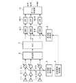
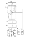
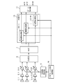
- FIG. 1 is a block diagram showing an example of the configuration of an antenna apparatus according to Embodiment 1 of the present invention.
- M is a natural number
- the antenna device includes an element antenna 1 (1-1 to 1-K (K is a natural number)), a low noise amplifier (LNA) 2 (2-1 to 2-K), Phase control unit 3 (3-1 to 3-K), phase value sequence acquisition unit 4, phase value setting unit 5, synthesis unit 6, AD converter (ADC) 7, frequency calculation unit 8, frequency conversion unit (DDC: A digital down converter (9-1 to 9-K), a filtering unit (LPF: Low Pass Filter) 10 (10-1 to 10-K), and a beam forming unit 11 are provided.
- K is a natural number
- LNA low noise amplifier
- Phase control unit 3 Phase value sequence acquisition unit 4
- phase value setting unit 5 phase value setting unit 6
- AD converter (ADC) 7 frequency calculation unit 8
- frequency conversion unit DDC: A digital down converter (9-1 to 9-K)
- LPF Low Pass Filter
- the element antenna 1 is provided with a plurality of systems and receives radio waves (signals).
- the LNA 2 is provided for each system and amplifies the signal received by the corresponding element antenna 1.
- the phase control unit 3 is a phase shifter that is provided for each system and controls the phase of the signal amplified by the corresponding LNA 2.
- the phase control unit 3 performs phase control with the phase value set by the phase value setting unit 5.
- the phase value sequence acquisition unit 4 obtains a phase value sequence to which a phase value that varies between systems and changes with time is given. At this time, the phase value sequence acquisition unit 4 may generate the phase value sequence itself, or may read data indicating the phase value sequence stored in a memory or the like.
- the phase value setting unit 5 sets the phase value in each phase control unit 3 based on the phase value sequence obtained by the phase value sequence acquisition unit 4.
- the phase value sequence acquisition unit 4, the phase value setting unit 5, and the frequency calculation unit 8 to be described later are executed by a program process using a CPU based on software.
- the synthesizing unit 6 synthesizes the signals whose phases are controlled by the phase control units 3 to generate a synthesized signal.
- the ADC 7 digitizes the combined signal generated by the combining unit 6.
- the frequency calculation unit 8 calculates a frequency shift amount for each system from the phase value sequence obtained by the phase value sequence acquisition unit 4.
- the DDC 9 is provided for each system, and performs frequency conversion on the combined signal digitized by the ADC 7 using the corresponding frequency shift amount calculated by the frequency calculation unit 8. At this time, the DDC 9 performs frequency conversion by down-converting the frequency of the synthesized signal by digital signal processing using the corresponding frequency shift amount.
- the LPF 10 is provided for each system, and performs low-pass filtering that allows a low-frequency to pass through the synthesized signal frequency-converted by the corresponding DDC 9. Thereby, the synthesized signal is separated into signals for each system.
- the beam forming unit 11 forms a beam signal using a signal subjected to low-pass filtering by each LPF 10.
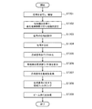
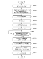
- each element antenna 1 receives a radio wave (signal), and each LNA 2 amplifies this signal (step ST201).
- the phase value sequence acquisition unit 4 obtains a phase value sequence that gives a phase value that varies between systems and changes with time, and the phase value setting unit 5 sets a phase value for each phase control unit 3 from this phase value sequence (Step ST202).
- each phase control unit 3 performs phase control on the signal amplified by the corresponding LNA 2 using the phase value set by the phase value setting unit 5 (step ST203).
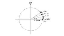
- each phase control unit 3 shifts the frequency of each signal by increasing the phase value with time instead of performing phase adjustment to align the phase wavefront.
- the phase value string acquisition unit 4 obtains a phase value string whose phase value increases with time.
- phase value ⁇ degree at time t is expressed as (t, ⁇ ), for example, the phase values are (0, 0), ( ⁇ t, 11.25), (2 ⁇ t, 22.5), (3 ⁇ t, 33.75). ), ...
- the phase is changed by 11.25 degrees at intervals of ⁇ t seconds, 32 ⁇ t seconds are required to rotate the 360 degree phase, and the frequency can be shifted by ⁇ 1 / (32 ⁇ t) Hz.
- the frequency is shifted by changing the phase value by a constant value at the control interval of the phase control unit 3. Assuming that the frequency of the signal before the frequency shift is f, the frequency of this signal is f ⁇ 1 / (32 ⁇ t) by the phase control unit 3.
- Each signal can be shifted to a different frequency by changing the amount of change in the phase value between the element antennas 1 or changing the control interval.
- phase control is performed with the above-described double phase change amount such as (0, 0), ( ⁇ t, 22.5), (2 ⁇ t, 45.0), (3 ⁇ t, 67.5),. .
- the phase is controlled at the control interval twice as described above as (0, 0), ( ⁇ t, 0), (2 ⁇ t, 11.25), (3 ⁇ t, 11.25),. Since the former rotates the phase by 22.5 degrees at intervals of ⁇ t seconds, the frequency can be shifted by 1 / (16 ⁇ t) Hz. Since the latter rotates the phase by 11.25 degrees at intervals of 2 ⁇ t seconds, the frequency can be shifted by 1 / (64 ⁇ t) Hz. In this way, the amount of phase change of each element antenna 1 is set to a different value.
- combining section 6 combines the signals whose phases are controlled by each phase control section 3 to generate a combined signal (frequency division multiplexed signal), and ADC 7 digitizes the combined signal (steps ST204 and 205). ). Thereby, a synthesized signal as shown in FIG. 4C can be obtained.
- the frequency calculation unit 8 calculates the frequency shift amount fs (fs (1) to fs (K)) for each system from the phase value sequence obtained by the phase value sequence acquisition unit 4 (step ST206).
- Examples of the frequency shift amount fs (k) (1 ⁇ k ⁇ K) in the k-th (1 ⁇ k ⁇ K) system are 1 / (32 ⁇ t), 1 / (16 ⁇ t), 1 / (64 ⁇ t). ).
- each DDC 9 performs frequency conversion on the synthesized signal digitized by the ADC 7 using the corresponding frequency shift amount calculated by the frequency calculation unit 8 (step ST207). At this time, the DDC 9 multiplies the composite signal by a complex sine wave having a frequency of f ⁇ fs (k) (1 ⁇ k ⁇ K) and performs frequency conversion.
- each LPF 10 performs low-pass filtering for allowing the low-pass frequency to pass through the synthesized signal frequency-converted by the corresponding DDC 9 (step ST208).
- filtering is performed so that signals of other systems are not included, and the synthesized signal is separated into signals for each system.
- the beam forming unit 11 forms a beam signal using the low-pass filtered signal by each LPF 10 (step ST209). That is, DBF processing is performed using signals separated for each system, and M beam signals are formed.
- each element antenna 1 can be controlled with high accuracy by digital signal processing to form a beam with a low side lobe.
- each phase control unit 3 frequency-division-multiplexes the signals of each system, synthesizes them, digitizes them, and separates them into signals of each system by digital signal processing. Therefore, it is possible to improve the SNR degradation over the conventional configuration. Further, since one ADC 7 can be provided, it is possible to realize cost reduction and power consumption reduction compared to the conventional configuration. Further, since the phase value of each phase control unit 3 is changed with time to frequency-division-multiplex the signals of each system, digital signal processing is improved even with an analog beam forming phased array antenna configuration. Thus, DBF can be realized.
- Embodiment 2 In the first embodiment, the case where the synthesized signal is separated for each system using the DDC 9 and the LPF 10 after being digitized by the ADC 7 has been described.
- each phase control unit 3 frequency-multiplexes the signals of each system by frequency shifting to frequencies having an orthogonal relationship, and performs discrete Fourier transform on the signals digitized by the ADC 7 to separate them. The case where it does is demonstrated.
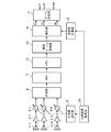
- FIG. 5 is a block diagram showing an example of the configuration of the antenna device according to Embodiment 2 of the present invention.
- the DDC 9 and the LPF 10 are removed from the antenna device according to the first embodiment shown in FIG. 1, and a memory 12, a discrete Fourier transform unit 13, and an extraction unit 14 are added.
- the phase value sequence acquisition unit 4 is changed to a phase value sequence acquisition unit 4b.
- Other configurations are the same, and only the different parts will be described with the same reference numerals.
- the phase value sequence acquisition unit 4b obtains a phase value sequence that gives a phase value that varies between systems and changes with time so as to shift to a frequency having an orthogonal relationship between systems.
- the phase value string acquisition unit 4b may generate the phase value string itself, or may be configured to read data indicating the phase value string stored in the memory or the like.
- phase value in each phase control unit 3 is set based on the phase value sequence obtained by the phase value sequence acquiring unit 4b. Further, the frequency calculation unit 8 in the second embodiment calculates the frequency shift amount for each system from the phase value sequence obtained by the phase value sequence acquisition unit 4b.
- the memory 12 records the synthesized signal digitized by the ADC 7 one by one.
- the discrete Fourier transform unit 13 reads the composite signal digitized by the ADC 7 from the memory 12 and performs frequency conversion by subjecting the composite signal to discrete Fourier transform.
- the extraction unit 14 extracts a signal corresponding to the frequency after the shift for each system based on each frequency shift amount calculated by the frequency calculation unit 8 from the signal frequency-converted by the discrete Fourier transform unit 13.
- the discrete Fourier transform unit 13 and the extraction unit 14 are executed by program processing using a CPU based on software.
- the beam forming unit 11 forms a beam signal using each signal extracted by the extracting unit 14.
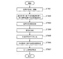
- each element antenna 1 receives a radio wave (signal), and each LNA 2 amplifies this signal (step ST601).
- the phase value sequence acquisition unit 4b obtains a phase value sequence giving a phase value that varies between systems and changes with time so as to shift to a frequency having an orthogonal relationship between systems, and the phase value setting unit 5 A phase value for each phase control unit 3 is set from the column (step ST602). For example, assuming that the frequency resolution that can be observed by the discrete Fourier transform in the subsequent stage is fres, a phase value sequence in which the frequency f ⁇ fs (k) (1 ⁇ k ⁇ K) after phase control is an integral multiple of fres is obtained. .
- each phase control unit 3 performs phase control on the signal amplified by the corresponding LNA 2 with the phase value set by the phase value setting unit 5 (step ST603).
- the combining unit 6 combines the signals whose phases are controlled by the respective phase control units 3 to generate a combined signal (frequency division multiplexed signal), the ADC 7 digitizes the combined signal, and the memory 12 stores the digital signal.
- the synthesized signals are recorded one by one (steps ST604 to ST606).
- step ST607 the discrete Fourier transform unit 13 determines whether the phases in all the phase control units 3 are rotated by 360 degrees or more.
- step ST607 when it is determined that the phases in all the phase control units 3 have not rotated 360 degrees or more, the sequence returns to step ST607 again and enters a standby state.
- step ST607 when the discrete Fourier transform unit 13 determines that the phases of all the phase control units 3 have rotated by 360 degrees or more, the composite signal digitized by the ADC 7 is read from the memory 12, Frequency conversion is performed by performing discrete Fourier transform on the synthesized signal (step ST608).
- the frequency calculation unit 8 calculates the frequency shift amount fs (fs (1) to fs (K)) for each system from the phase value sequence generated by the phase value sequence acquisition unit 4b (step ST609).
- the extraction unit 14 extracts a signal corresponding to the frequency after the shift for each system based on each frequency shift amount calculated by the frequency calculation unit 8 from the signal frequency-converted by the discrete Fourier transform unit 13 (step) ST610). That is, since complex information (amplitude and phase) of orthogonal frequency components can be obtained by discrete Fourier transform, the extraction unit 14 outputs complex information of a frequency shifted by the frequency shift amount obtained by the frequency calculation unit 8. . Thereby, the synthesized signal can be separated into signals for each system.
- the beam forming unit 11 forms a beam signal using each signal extracted by the extracting unit 14 (step ST611).
- each phase control unit 3 frequency-division-multiplexes the signals of each system, synthesizes them, digitizes them, and separates them into signals of each system by digital signal processing. Therefore, the same effect as in the first embodiment can be obtained.
- each phase control unit 3 is configured to frequency-division-multiplex the signals of each system by shifting the frequency of each system to an orthogonal frequency, so that the signals of each system are separated from the frequency-division multiplexed signal. Discrete Fourier transform can be used for the processing to be performed, and the load of digital signal processing can be reduced compared to the first embodiment.
- Embodiment 3 In the first and second embodiments, the case where the phase value in each phase control unit 3 is changed over time and the signal of each system is frequency-shifted has been described.
- the phase value sequence acquisition unit 4c obtains a phase value sequence based on the orthogonal code, and uses the phase value sequence to control the phase of the signals of each system to be orthogonalized and synthesized. That is, the case where the signals of each system are code-division multiplexed and separated by digital signal processing is shown.
- FIG. 7 is a block diagram showing an example of the configuration of the antenna device according to Embodiment 3 of the present invention.
- the antenna apparatus according to the third embodiment shown in FIG. 7 removes the DDC 9 and the LPF 10 from the antenna apparatus according to the first embodiment shown in FIG. 1 and adds a separation unit 15 to make the phase value sequence acquisition unit 4 a phase value.
- the column acquisition unit 4c is changed.
- Other configurations are the same, and only different parts will be described.
- the phase value sequence acquisition unit 4c obtains a phase value sequence having an orthogonal relationship between systems and giving a time-varying phase value based on the orthogonal code.
- the phase value string acquisition unit 4c may generate the phase value string itself, or may be configured to read data indicating the phase value string stored in the memory or the like.
- the phase value in each phase control unit 3 is set based on the phase value sequence obtained by the phase value sequence acquisition unit 4c.
- the separation unit 15 includes a correlation processing unit 151 (151-1 to 151 -K) for each system, and the synthesized signal digitized by the ADC 7 and the phase value sequence obtained by the phase value sequence acquisition unit 4 c By performing correlation processing, the signal is separated into signals for each system. At this time, the separation unit 15 performs the convolution operation in the time domain using the synthesized signal digitized by the ADC 7 and the phase value sequence obtained by the phase value sequence acquisition unit 4c, thereby obtaining the correlation. Process. Alternatively, the separation unit 15 uses the signal digitized by the ADC 7 and the phase value sequence obtained by the phase value sequence acquisition unit 4c to perform the inner product operation of the Fourier transform in the frequency domain, thereby performing the above correlation. Processing may be performed. The phase value sequence acquisition unit 4c and the separation unit 15 are executed by a program process using a CPU based on software.
- the beam forming unit 11 forms a beam signal using each signal separated by the separating unit 15.
- each element antenna 1 receives a radio wave (signal), and each LNA 2 amplifies this signal (step ST801).
- the phase value sequence acquisition unit 4c obtains a phase value sequence having an orthogonal relationship between systems based on the orthogonal code and giving a phase value that changes with time, and the phase value setting unit 5 determines each phase from the phase value sequence.
- a phase value for the control unit 3 is set (step ST802). That is, the phase value sequence acquisition unit 4c generates code pattern groups that are orthogonal to each other between the systems. At this time, the value that each code can take may be multi-value or binary.
- each phase control unit 3 performs phase control on the signal amplified by the corresponding LNA 2 with the phase value set by the phase value setting unit 5 (step ST803).
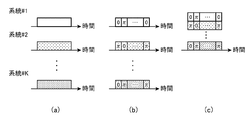
- the orthogonal code is binary, as shown in FIGS. 9A and 9B, the orthogonal code corresponding to the k (1 ⁇ k ⁇ K) -th element antenna 1-k is 1.
- the phase value of the phase control unit 3-k is 0 degrees, and when the sign is -1, sets the phase value to 180 degrees ( ⁇ [rad]).
- combining section 6 combines the signals whose phases are controlled by each phase control section 3 to generate a combined signal (code division multiplexed signal), and ADC 7 digitizes the combined signal (steps ST804 and 805). ). Thereby, a synthesized signal as shown in FIG. 9C can be obtained.
- the separation unit 15 performs a correlation process between the combined signal digitized by the ADC 7 and the phase value sequence obtained by the phase value sequence acquisition unit 4c by each correlation processing unit 151, thereby obtaining a signal for each system. (Step ST806). At this time, as shown in FIG. 9, since the signals of each system are orthogonalized, it can be separated into signals of each system by this correlation processing.
- beam forming section 11 forms a beam signal using each signal separated by separating section 15 (step ST807).
- signals of each system are orthogonally encoded by each phase control unit 3 and code division multiplexed, combined, digitized, and separated into signals of each system by correlation processing. Since it did in this way, degradation of SNR can be improved with respect to a conventional structure. Further, since one ADC 7 can be provided, it is possible to realize cost reduction and power consumption reduction compared to the conventional configuration. In addition, since the signal of each system is code division multiplexed by changing the phase value of each phase control unit 3 over time, digital signal processing is improved even with an analog beam forming phased array antenna configuration. Thus, DBF can be realized. In the third embodiment, since the code division multiplexing is performed by each phase control unit 3, it is not necessary to expand the processing band of the ADC 7. Therefore, DBF can be realized without using an expensive ADC 7.
- FIG. FIG. 10 is a block diagram showing an example of the configuration of the antenna device according to Embodiment 4 of the present invention.
- the antenna device according to Embodiment 4 shown in FIG. 10 uses Hadamard matrix acquisition unit 16 as phase value sequence acquisition unit 4c of the antenna device according to Embodiment 3 shown in FIG.
- Other configurations are the same, and only the different parts are described with the same reference numerals.
- the Hadamard matrix acquisition unit 16 obtains a Hadamard matrix having a dimension equal to or greater than the number of systems as a phase value sequence based on orthogonal codes. At this time, the Hadamard matrix acquisition unit 16 may generate the Hadamard matrix by itself or may read out data indicating the Hadamard matrix stored in the memory or the like.
- each correlation processing unit 151 performs correlation processing between the combined signal digitized by the ADC 7 and the Hadamard matrix obtained by the Hadamard matrix acquisition unit 16, thereby generating a system Separate each signal.
- the operation of the antenna device according to the fourth embodiment is the same except that the operation of the phase value sequence acquisition unit 4c of the operation of the antenna device according to the third embodiment is replaced with the operation of the Hadamard matrix acquisition unit 16. The description is omitted.
- This Hadamard matrix is a square matrix, and the element value of the matrix is either +1 or -1. Any two arbitrary row vectors are orthogonal to each other.
- This Hadamard matrix can be calculated by the following equation (1).
- each row vector is an orthogonal code sequence of each system. Then, the case where the element value is 1 corresponds to a phase value of 0 degrees, and the case where the element value is ⁇ 1 corresponds to a phase value of 180 degrees. In this case, for example, the phase value of the received signal of the second system is controlled as (0 degree, 180 degree, 0 degree, 180 degree).
- an orthogonal code can be formed with two kinds of phase values of 0 degrees and 180 degrees, and this code is applied regardless of the number of bits of the phase shifter used in each phase control unit 3. Can do.
- the order of the Hadamard matrix is an even number. Therefore, when the system number K is an odd number, an even-order Hadamard matrix exceeding the system number K is generated, and K row vectors among them are used as orthogonal codes of each system.
- the fourth embodiment even if a Hadamard matrix is used as the phase value sequence, the same effect as in the third embodiment can be obtained.
- the phase since the phase is controlled by a binary phase value sequence, the number of bits of each phase control unit 3 can be reduced, and DBF can be realized at low cost.
- the antenna device improves the SNR degradation, can realize lower cost and lower power consumption than the conventional configuration, can improve the SNR degradation, and is an analog beam forming phased array antenna Since the configuration can also realize DBF, it is suitable for use in an antenna device or the like that performs DBF that forms a beam with a digital signal.
Landscapes
- Engineering & Computer Science (AREA)
- Computer Networks & Wireless Communication (AREA)
- Signal Processing (AREA)
- Variable-Direction Aerials And Aerial Arrays (AREA)
- Radio Transmission System (AREA)
Abstract
Description
実施の形態1.
図1はこの発明の実施の形態1のアンテナ装置の構成の一例を示すブロック図である。以下では、アンテナ装置がM(Mは自然数)本のビームを形成する場合を例に説明を行う。
アンテナ装置は、図1に示すように、素子アンテナ1(1-1~1-K(Kは自然数))、低雑音増幅器(LNA:Low Noise Amplifier)2(2-1~2-K)、位相制御部3(3-1~3-K)、位相値列取得部4、位相値設定部5、合成部6、AD変換器(ADC)7、周波数計算部8、周波数変換部(DDC:Digital Down Converter)9(9-1~9-K)、フィルタリング部(LPF:Low Pass Filter)10(10-1~10-K)及びビーム形成部11を備えている。
LNA2は、系統毎に設けられ、対応する素子アンテナ1により受信された信号を増幅するものである。
位相値設定部5は、位相値列取得部4により得られた位相値列に基づき、各位相制御部3での位相値を設定するものである。
なお、位相値列取得部4、位相値設定部5及び後述する周波数計算部8は、ソフトウェアに基づくCPUを用いたプログラム処理によって実行される。
ADC7は、合成部6により生成された合成信号をデジタル化するものである。
DDC9は、系統毎に設けられ、ADC7によりデジタル化された合成信号に対し、周波数計算部8により算出された対応する周波数シフト量を用いて周波数変換を行うものである。この際、DDC9は、対応する周波数シフト量を用いて、合成信号の周波数をデジタル信号処理でダウンコンバートすることで周波数変換を行う。
ビーム形成部11は、各LPF10により低域フィルタリングが行われた信号を用いて、ビーム信号を形成するものである。
実施の形態1に係るアンテナ装置の動作では、図2に示すように、まず、各素子アンテナ1は電波(信号)を受信し、各LNA2はこの信号を増幅する(ステップST201)。
次いで、各位相制御部3は、対応するLNA2により増幅された信号に対し、位相値設定部5により設定された位相値で位相制御を行う(ステップST203)。
実施の形態1では、ADC7でデジタル化した後に、DDC9及びLPF10を用いて合成信号を系統毎に分離する場合について示した。それに対し、実施の形態2では、各位相制御部3において、直交関係を有する周波数に各系統の信号を周波数シフトさせて周波数多重し、ADC7でデジタル化した信号に対し離散フーリエ変換を施して分離する場合について説明する。
離散フーリエ変換部13は、ADC7によりデジタル化された合成信号をメモリ12から読出し、この合成信号を離散フーリエ変換することで周波数変換するものである。
なお、離散フーリエ変換部13及び抽出部14は、ソフトウェアに基づくCPUを用いたプログラム処理によって実行される。
実施の形態2に係るアンテナ装置の動作では、図6に示すように、まず、各素子アンテナ1は電波(信号)を受信し、各LNA2はこの信号を増幅する(ステップST601)。
次いで、各位相制御部3は、対応するLNA2により増幅された信号に対し、位相値設定部5により設定された位相値で位相制御を行う(ステップST603)。
また、実施の形態2では、各位相制御部3により、各系統の信号を直交周波数に周波数シフトして周波数分割多重するように構成したので、周波数分割多重された信号から各系統の信号を分離する処理に離散フーリエ変換を用いることができ、実施の形態1に対して、デジタル信号処理の負荷を低減することができる。
実施の形態1,2では、各位相制御部3での位相値を時間変化させ、各系統の信号を周波数シフトさせる場合について示した。それに対し、実施の形態3では、位相値列取得部4cで直交符号に基づく位相値列を得て、この位相値列を用いて各系統の信号の位相を制御して直交化し合成する。すなわち、各系統の信号を符号分割多重しデジタル信号処理で分離する場合について示す。
なお、実施の形態3における位相値設定部5では、位相値列取得部4cにより得られた位相値列に基づき、各位相制御部3での位相値を設定する。
この際、分離部15は、ADC7によりデジタル化された合成信号と、位相値列取得部4cにより得られた位相値列とを用いて、時間領域での畳込み演算を行うことで、上記相関処理を行う。又は、分離部15は、ADC7によりデジタル化された信号と、位相値列取得部4cにより得られた位相値列とを用いて、周波数領域でのフーリエ変換の内積演算を行うことで、上記相関処理を行ってもよい。
なお、位相値列取得部4c及び分離部15は、ソフトウェアに基づくCPUを用いたプログラム処理によって実行される。
実施の形態3に係るアンテナ装置の動作では、図8に示すように、まず、各素子アンテナ1は電波(信号)を受信し、各LNA2はこの信号を増幅する(ステップST801)。
また、実施の形態3では、各位相制御部3により符号分割多重するのでADC7の処理帯域を拡大する必要はない。そのため、高価なADC7を使用せずにDBFを実現できる。
図10はこの発明の実施の形態4に係るアンテナ装置の構成の一例を示すブロック図である。図10に示す実施の形態4に係るアンテナ装置は、図7に示す実施の形態3に係るアンテナ装置の位相値列取得部4cとしてアダマール行列取得部16を用いたものである。その他の構成は同様であり、同一の符号を付して異なる部分についてのみ説明を行う。


また、実施の形態4では、2値の位相値列で位相を制御するため、各位相制御部3のビット数を小さくでき、低コストでDBFを実現できる。
Claims (10)
- 複数系統設けられ、信号を受信する素子アンテナと、
前記系統毎に設けられ、対応する前記素子アンテナにより受信された信号の位相を制御する位相制御部と、
前記系統間で異なり且つ時間変化する位相値を与えた位相値列を得る位相値列取得部と、
前記位相値列取得部により得られた位相値列に基づき、各々の前記位相制御部での位相値を設定する位相値設定部と、
各々の前記位相制御部により位相が制御された信号を合成する合成部と、
前記合成部により合成された信号をデジタル化するAD変換部と、
前記位相値列取得部により得られた位相値列から前記系統毎の周波数シフト量を算出する周波数計算部と、
前記系統毎に設けられ、前記AD変換部によりデジタル化された信号に対し、前記周波数計算部により算出された対応する周波数シフト量を用いて周波数変換を行う周波数変換部と、
前記系統毎に設けられ、対応する前記周波数変換部により周波数変換された信号に対して低域フィルタリングを行うフィルタリング部と、
各々の前記フィルタリング部により低域フィルタリングが行われた信号を用いて、ビーム信号を形成するビーム形成部と
を備えたアンテナ装置。 - 前記位相制御部は移相器である
ことを特徴とする請求項1記載のアンテナ装置。 - 複数系統設けられ、信号を受信する素子アンテナと、
前記系統毎に設けられ、対応する前記素子アンテナにより受信された信号の位相を制御する位相制御部と、
前記系統間で直交関係を有する周波数にシフトするよう、当該系統間で異なり且つ時間変化する位相値を与えた位相値列を得る位相値列取得部と、
前記位相値列取得部により得られた位相値列に基づき、各々の前記位相制御部での位相値を設定する位相値設定部と、
各々の前記位相制御部により位相が制御された信号を合成する合成部と、
前記合成部により合成された信号をデジタル化するAD変換部と、
前記AD変換部によりデジタル化された信号を周波数変換する離散フーリエ変換部と、
前記位相値列取得部により得られた位相値列から前記系統毎の周波数シフト量を算出する周波数計算部と、
前記離散フーリエ変換部により周波数変換された信号から、前記周波数計算部により計算された各周波数シフト量に基づく前記系統毎のシフト後の周波数に対応する信号を抽出する抽出部と、
前記抽出部により抽出された各信号を用いて、ビーム信号を形成するビーム形成部と
を備えたアンテナ装置。 - 前記位相制御部は移相器である
ことを特徴とする請求項3記載のアンテナ装置。 - 複数系統設けられ、信号を受信する素子アンテナと、
前記系統毎に設けられ、対応する前記素子アンテナにより受信された信号の位相を制御する位相制御部と、
直交符号に基づき、前記系統間で直交関係を有し且つ時間変化する位相値を与えた位相値列を得る位相値列取得部と、
前記位相値列取得部により得られた位相値列に基づき、各々の前記位相制御部での位相値を設定する位相値設定部と、
各々の前記位相制御部により位相が制御された信号を合成する合成部と、
前記合成部により合成された信号をデジタル化するAD変換部と、
前記AD変換部によりデジタル化された信号と、前記位相値列取得部により得られた位相値列との相関処理を行うことで、前記系統毎の信号に分離する分離部と、
前記分離部により分離された各信号を用いて、ビーム信号を形成するビーム形成部と
を備えたアンテナ装置。 - 前記位相制御部は移相器である
ことを特徴とする請求項5記載のアンテナ装置。 - 前記位相値列取得部は、2値の前記直交符号に基づき、180度異なる位相値を割り当てた前記位相値列を得る
ことを特徴とする請求項5記載のアンテナ装置。 - 前記位相値列取得部は、前記位相値列として前記系統数以上の次元のアダマール行列を得るアダマール行列取得部である
ことを特徴とする請求項5記載のアンテナ装置。 - 前記分離部は、前記AD変換部によりデジタル化された信号と、前記位相値列取得部により得られた位相値列とを用いて、時間領域での畳込み演算を行うことで、前記相関処理を行う
ことを特徴とする請求項5記載のアンテナ装置。 - 前記分離部は、前記AD変換部によりデジタル化された信号と、前記位相値列取得部により得られた位相値列とを用いて、周波数領域でのフーリエ変換の内積演算を行うことで、前記相関処理を行う
ことを特徴とする請求項5記載のアンテナ装置。
Priority Applications (4)
| Application Number | Priority Date | Filing Date | Title |
|---|---|---|---|
| JP2016573160A JP6297177B2 (ja) | 2015-02-06 | 2015-02-06 | アンテナ装置 |
| US15/539,765 US10284239B2 (en) | 2015-02-06 | 2015-02-06 | Antenna device |
| PCT/JP2015/053399 WO2016125305A1 (ja) | 2015-02-06 | 2015-02-06 | アンテナ装置 |
| EP15881122.4A EP3244551B1 (en) | 2015-02-06 | 2015-02-06 | Antenna device |
Applications Claiming Priority (1)
| Application Number | Priority Date | Filing Date | Title |
|---|---|---|---|
| PCT/JP2015/053399 WO2016125305A1 (ja) | 2015-02-06 | 2015-02-06 | アンテナ装置 |
Publications (1)
| Publication Number | Publication Date |
|---|---|
| WO2016125305A1 true WO2016125305A1 (ja) | 2016-08-11 |
Family
ID=56563669
Family Applications (1)
| Application Number | Title | Priority Date | Filing Date |
|---|---|---|---|
| PCT/JP2015/053399 Ceased WO2016125305A1 (ja) | 2015-02-06 | 2015-02-06 | アンテナ装置 |
Country Status (4)
| Country | Link |
|---|---|
| US (1) | US10284239B2 (ja) |
| EP (1) | EP3244551B1 (ja) |
| JP (1) | JP6297177B2 (ja) |
| WO (1) | WO2016125305A1 (ja) |
Cited By (2)
| Publication number | Priority date | Publication date | Assignee | Title |
|---|---|---|---|---|
| CN107104710A (zh) * | 2017-03-28 | 2017-08-29 | 重庆大学 | 一种数字相控阵天线的波束合成方法 |
| JP2024505071A (ja) * | 2021-01-28 | 2024-02-02 | セミコンダクター コンポーネンツ インダストリーズ エルエルシー | Mimoチャネルエクステンダと関連システムおよび方法 |
Families Citing this family (4)
| Publication number | Priority date | Publication date | Assignee | Title |
|---|---|---|---|---|
| JP2017152830A (ja) * | 2016-02-23 | 2017-08-31 | Kddi株式会社 | 無線通信システム、送信装置、受信装置、及び通信方法 |
| CN111869291B (zh) | 2018-02-02 | 2025-05-09 | 康奈尔大学 | 无线系统中的信道制图 |
| US10608686B1 (en) * | 2019-07-02 | 2020-03-31 | Cornell University | Circuit and method for enabling channel denoising in a wireless communication apparatus |
| CN113852383B (zh) * | 2021-09-23 | 2022-08-09 | 上海航天电子通讯设备研究所 | 一种vhf频段突发信号的抗干扰处理系统 |
Citations (5)
| Publication number | Priority date | Publication date | Assignee | Title |
|---|---|---|---|---|
| JP2000101494A (ja) * | 1998-09-25 | 2000-04-07 | Nec Saitama Ltd | 無線装置とその無線受信方法 |
| JP2003032144A (ja) * | 2001-07-17 | 2003-01-31 | Furuno Electric Co Ltd | スペクトル拡散信号捕捉装置および方法 |
| JP2003134017A (ja) * | 2001-10-19 | 2003-05-09 | Mitsubishi Electric Corp | ディジタルビームフォーミングアンテナ装置 |
| JP2003521822A (ja) * | 1997-09-15 | 2003-07-15 | メタウエイブ・コミュニケーションズ・コーポレイション | Cdma通信容量を改善するための実用的な空間−時間無線方法 |
| JP2005260720A (ja) * | 2004-03-12 | 2005-09-22 | Mitsubishi Electric Corp | 無線受信装置 |
Family Cites Families (17)
| Publication number | Priority date | Publication date | Assignee | Title |
|---|---|---|---|---|
| US6108565A (en) | 1997-09-15 | 2000-08-22 | Adaptive Telecom, Inc. | Practical space-time radio method for CDMA communication capacity enhancement |
| JP3335953B2 (ja) | 1999-02-05 | 2002-10-21 | 埼玉日本電気株式会社 | 符号分割多元接続システムにおける基地局 |
| CN100385826C (zh) * | 2002-06-24 | 2008-04-30 | 美国博通公司 | 采用多路复用接收链处理的降低复杂度的天线系统 |
| US20040087294A1 (en) * | 2002-11-04 | 2004-05-06 | Tia Mobile, Inc. | Phases array communication system utilizing variable frequency oscillator and delay line network for phase shift compensation |
| US7869528B2 (en) * | 2003-10-31 | 2011-01-11 | Northrop Grumman Systems Corporation | Multi-carrier transceiver assembly |
| JP4699843B2 (ja) * | 2005-09-15 | 2011-06-15 | 富士通株式会社 | 移動通信システム、並びに移動通信システムにおいて使用される基地局装置および移動局装置 |
| US7898478B2 (en) * | 2007-02-28 | 2011-03-01 | Samsung Electronics Co., Ltd. | Method and system for analog beamforming in wireless communication systems |
| EP2143214A2 (en) * | 2007-05-10 | 2010-01-13 | Astrium Limited | Signal processing system |
| US10142855B2 (en) * | 2007-05-21 | 2018-11-27 | Spatial Digital Systems, Inc. | Channel bonding using K-muxing and multiple-beam antenna |
| US7714781B2 (en) * | 2007-09-05 | 2010-05-11 | Samsung Electronics Co., Ltd. | Method and system for analog beamforming in wireless communication systems |
| US7859459B2 (en) * | 2008-04-04 | 2010-12-28 | Panasonic Corporation | Phased array receivers and methods employing phase shifting downconverters |
| US8195118B2 (en) * | 2008-07-15 | 2012-06-05 | Linear Signal, Inc. | Apparatus, system, and method for integrated phase shifting and amplitude control of phased array signals |
| US8223889B2 (en) * | 2009-01-09 | 2012-07-17 | Empire Technology Development, Llc | Opportunistic radio frequency communications |
| US8576768B2 (en) * | 2009-04-16 | 2013-11-05 | Qualcomm Incorporated | Hybrid multi-band receiver |
| KR101079549B1 (ko) * | 2009-08-06 | 2011-11-02 | 고려대학교 산학협력단 | 적응형 빔포밍을 이용한 다중 안테나 시스템 |
| JP5729561B2 (ja) | 2011-08-31 | 2015-06-03 | 株式会社東海理化電機製作所 | 時分割多重アダプティブアレーアンテナの信号処理装置 |
| EP2675080B1 (en) * | 2012-06-15 | 2019-06-12 | IMEC vzw | A phased-array receiver for mm-wave applications |
-
2015
- 2015-02-06 WO PCT/JP2015/053399 patent/WO2016125305A1/ja not_active Ceased
- 2015-02-06 US US15/539,765 patent/US10284239B2/en active Active
- 2015-02-06 JP JP2016573160A patent/JP6297177B2/ja active Active
- 2015-02-06 EP EP15881122.4A patent/EP3244551B1/en active Active
Patent Citations (5)
| Publication number | Priority date | Publication date | Assignee | Title |
|---|---|---|---|---|
| JP2003521822A (ja) * | 1997-09-15 | 2003-07-15 | メタウエイブ・コミュニケーションズ・コーポレイション | Cdma通信容量を改善するための実用的な空間−時間無線方法 |
| JP2000101494A (ja) * | 1998-09-25 | 2000-04-07 | Nec Saitama Ltd | 無線装置とその無線受信方法 |
| JP2003032144A (ja) * | 2001-07-17 | 2003-01-31 | Furuno Electric Co Ltd | スペクトル拡散信号捕捉装置および方法 |
| JP2003134017A (ja) * | 2001-10-19 | 2003-05-09 | Mitsubishi Electric Corp | ディジタルビームフォーミングアンテナ装置 |
| JP2005260720A (ja) * | 2004-03-12 | 2005-09-22 | Mitsubishi Electric Corp | 無線受信装置 |
Cited By (3)
| Publication number | Priority date | Publication date | Assignee | Title |
|---|---|---|---|---|
| CN107104710A (zh) * | 2017-03-28 | 2017-08-29 | 重庆大学 | 一种数字相控阵天线的波束合成方法 |
| CN107104710B (zh) * | 2017-03-28 | 2020-05-22 | 重庆大学 | 一种数字相控阵天线的波束合成方法 |
| JP2024505071A (ja) * | 2021-01-28 | 2024-02-02 | セミコンダクター コンポーネンツ インダストリーズ エルエルシー | Mimoチャネルエクステンダと関連システムおよび方法 |
Also Published As
| Publication number | Publication date |
|---|---|
| US20180269911A1 (en) | 2018-09-20 |
| EP3244551A1 (en) | 2017-11-15 |
| US10284239B2 (en) | 2019-05-07 |
| EP3244551A4 (en) | 2018-10-10 |
| JPWO2016125305A1 (ja) | 2017-06-22 |
| JP6297177B2 (ja) | 2018-03-20 |
| EP3244551B1 (en) | 2020-03-25 |
Similar Documents
| Publication | Publication Date | Title |
|---|---|---|
| JP6297177B2 (ja) | アンテナ装置 | |
| KR100555166B1 (ko) | 다중 브랜치 수신기 시스템 및 방법 | |
| JP6909023B2 (ja) | レーダ装置及びレーダ方法 | |
| US10965023B2 (en) | Programmable beamforming system including element-level analog channelizer | |
| JP2004518137A5 (ja) | ||
| JP2009300284A (ja) | 到来電波方位測定装置、到来電波方位測定方法及び到来電波方位測定プログラム | |
| CN101132493A (zh) | 集成调谐器装置、系统和方法 | |
| JP2015025668A (ja) | レーダ装置 | |
| JP2008312197A (ja) | アダプティブアレーアンテナ装置及びその指向性制御方法 | |
| US20190089054A1 (en) | Techniques and Methods for Adaptive Removal of Analog Phase Errors in Frequency Division Multiplexed Digital Beam-Formers | |
| CN102647197A (zh) | 多频段数字相控阵接收天线的信道化方法 | |
| US7953184B2 (en) | Direct sampling type wireless receiver and method using the same | |
| JP2000201135A (ja) | 無線受信装置および逆拡散器 | |
| EP1089512A1 (en) | Telecommunication device with analog fourier transformation unit | |
| JP2007006219A (ja) | アダプティブアンテナ装置 | |
| JP2013181864A (ja) | 合成開口レーダ装置および信号処理装置 | |
| JP2002185378A (ja) | アレーアンテナ装置 | |
| JP3160580B2 (ja) | アンテナ分解能を向上させた電波受信装置 | |
| Manteghi et al. | A novel technique for a low-cost digital phased array design | |
| JP5814134B2 (ja) | アレーアンテナ | |
| CN112653424A (zh) | 一种信号处理方法、设备和计算机可读存储介质 | |
| Huang et al. | Beamspace SMILE array for digital beamforming with a single RF receiver | |
| JP2005142892A (ja) | マルチモード無線通信装置 | |
| CA3089696A1 (en) | Transmission device, wireless communication system, and transmission method | |
| JP2014143654A (ja) | 受信装置、受信方法および周波数誤差推定回路 |
Legal Events
| Date | Code | Title | Description |
|---|---|---|---|
| 121 | Ep: the epo has been informed by wipo that ep was designated in this application |
Ref document number: 15881122 Country of ref document: EP Kind code of ref document: A1 |
|
| ENP | Entry into the national phase |
Ref document number: 2016573160 Country of ref document: JP Kind code of ref document: A |
|
| WWE | Wipo information: entry into national phase |
Ref document number: 15539765 Country of ref document: US |
|
| REEP | Request for entry into the european phase |
Ref document number: 2015881122 Country of ref document: EP |
|
| NENP | Non-entry into the national phase |
Ref country code: DE |