WO2016125531A1 - Module - Google Patents
Module Download PDFInfo
- Publication number
- WO2016125531A1 WO2016125531A1 PCT/JP2016/050459 JP2016050459W WO2016125531A1 WO 2016125531 A1 WO2016125531 A1 WO 2016125531A1 JP 2016050459 W JP2016050459 W JP 2016050459W WO 2016125531 A1 WO2016125531 A1 WO 2016125531A1
- Authority
- WO
- WIPO (PCT)
- Prior art keywords
- coil core
- wiring board
- coil
- wiring
- insulating layer
- Prior art date
- Legal status (The legal status is an assumption and is not a legal conclusion. Google has not performed a legal analysis and makes no representation as to the accuracy of the status listed.)
- Ceased
Links
Images


Classifications
-
- H—ELECTRICITY
- H05—ELECTRIC TECHNIQUES NOT OTHERWISE PROVIDED FOR
- H05K—PRINTED CIRCUITS; CASINGS OR CONSTRUCTIONAL DETAILS OF ELECTRIC APPARATUS; MANUFACTURE OF ASSEMBLAGES OF ELECTRICAL COMPONENTS
- H05K1/00—Printed circuits
- H05K1/18—Printed circuits structurally associated with non-printed electric components
- H05K1/182—Printed circuits structurally associated with non-printed electric components associated with components mounted in printed circuit boards [PCB], e.g. insert-mounted components [IMC]
- H05K1/185—Printed circuits structurally associated with non-printed electric components associated with components mounted in printed circuit boards [PCB], e.g. insert-mounted components [IMC] associated with components encapsulated in the insulating substrate of the PCBs; associated with components incorporated in internal layers of multilayer circuit boards
-
- H—ELECTRICITY
- H05—ELECTRIC TECHNIQUES NOT OTHERWISE PROVIDED FOR
- H05K—PRINTED CIRCUITS; CASINGS OR CONSTRUCTIONAL DETAILS OF ELECTRIC APPARATUS; MANUFACTURE OF ASSEMBLAGES OF ELECTRICAL COMPONENTS
- H05K1/00—Printed circuits
- H05K1/18—Printed circuits structurally associated with non-printed electric components
- H05K1/182—Printed circuits structurally associated with non-printed electric components associated with components mounted in printed circuit boards [PCB], e.g. insert-mounted components [IMC]
-
- H—ELECTRICITY
- H01—ELECTRIC ELEMENTS
- H01F—MAGNETS; INDUCTANCES; TRANSFORMERS; SELECTION OF MATERIALS FOR THEIR MAGNETIC PROPERTIES
- H01F17/00—Fixed inductances of the signal type
- H01F17/0006—Printed inductances
- H01F17/0033—Printed inductances with the coil helically wound around a magnetic core
-
- H—ELECTRICITY
- H01—ELECTRIC ELEMENTS
- H01F—MAGNETS; INDUCTANCES; TRANSFORMERS; SELECTION OF MATERIALS FOR THEIR MAGNETIC PROPERTIES
- H01F17/00—Fixed inductances of the signal type
- H01F17/04—Fixed inductances of the signal type with magnetic core
- H01F17/06—Fixed inductances of the signal type with magnetic core with core substantially closed in itself, e.g. toroid
- H01F17/062—Toroidal core with turns of coil around it
-
- H—ELECTRICITY
- H01—ELECTRIC ELEMENTS
- H01F—MAGNETS; INDUCTANCES; TRANSFORMERS; SELECTION OF MATERIALS FOR THEIR MAGNETIC PROPERTIES
- H01F27/00—Details of transformers or inductances, in general
- H01F27/28—Coils; Windings; Conductive connections
- H01F27/2804—Printed windings
-
- H—ELECTRICITY
- H01—ELECTRIC ELEMENTS
- H01F—MAGNETS; INDUCTANCES; TRANSFORMERS; SELECTION OF MATERIALS FOR THEIR MAGNETIC PROPERTIES
- H01F27/00—Details of transformers or inductances, in general
- H01F27/28—Coils; Windings; Conductive connections
- H01F27/2895—Windings disposed upon ring cores
-
- H—ELECTRICITY
- H05—ELECTRIC TECHNIQUES NOT OTHERWISE PROVIDED FOR
- H05K—PRINTED CIRCUITS; CASINGS OR CONSTRUCTIONAL DETAILS OF ELECTRIC APPARATUS; MANUFACTURE OF ASSEMBLAGES OF ELECTRICAL COMPONENTS
- H05K1/00—Printed circuits
- H05K1/16—Printed circuits incorporating printed electric components, e.g. printed resistors, capacitors or inductors
- H05K1/165—Printed circuits incorporating printed electric components, e.g. printed resistors, capacitors or inductors incorporating printed inductors
-
- H—ELECTRICITY
- H01—ELECTRIC ELEMENTS
- H01F—MAGNETS; INDUCTANCES; TRANSFORMERS; SELECTION OF MATERIALS FOR THEIR MAGNETIC PROPERTIES
- H01F17/00—Fixed inductances of the signal type
- H01F17/0006—Printed inductances
- H01F2017/0086—Printed inductances on semiconductor substrate
-
- H—ELECTRICITY
- H01—ELECTRIC ELEMENTS
- H01F—MAGNETS; INDUCTANCES; TRANSFORMERS; SELECTION OF MATERIALS FOR THEIR MAGNETIC PROPERTIES
- H01F27/00—Details of transformers or inductances, in general
- H01F27/06—Mounting, supporting or suspending transformers, reactors or choke coils not being of the signal type
- H01F2027/065—Mounting on printed circuit boards
-
- H—ELECTRICITY
- H01—ELECTRIC ELEMENTS
- H01F—MAGNETS; INDUCTANCES; TRANSFORMERS; SELECTION OF MATERIALS FOR THEIR MAGNETIC PROPERTIES
- H01F27/00—Details of transformers or inductances, in general
- H01F27/28—Coils; Windings; Conductive connections
- H01F27/2804—Printed windings
- H01F2027/2809—Printed windings on stacked layers
-
- H—ELECTRICITY
- H05—ELECTRIC TECHNIQUES NOT OTHERWISE PROVIDED FOR
- H05K—PRINTED CIRCUITS; CASINGS OR CONSTRUCTIONAL DETAILS OF ELECTRIC APPARATUS; MANUFACTURE OF ASSEMBLAGES OF ELECTRICAL COMPONENTS
- H05K2201/00—Indexing scheme relating to printed circuits covered by H05K1/00
- H05K2201/08—Magnetic details
- H05K2201/083—Magnetic materials
- H05K2201/086—Magnetic materials for inductive purposes, e.g. printed inductor with ferrite core
-
- H—ELECTRICITY
- H05—ELECTRIC TECHNIQUES NOT OTHERWISE PROVIDED FOR
- H05K—PRINTED CIRCUITS; CASINGS OR CONSTRUCTIONAL DETAILS OF ELECTRIC APPARATUS; MANUFACTURE OF ASSEMBLAGES OF ELECTRICAL COMPONENTS
- H05K2201/00—Indexing scheme relating to printed circuits covered by H05K1/00
- H05K2201/10—Details of components or other objects attached to or integrated in a printed circuit board
- H05K2201/10007—Types of components
- H05K2201/10015—Non-printed capacitor
Definitions
- the present invention relates to a module including a coil and an electronic component.
- the circuit board is mounted on a wiring board, an insulating layer in which the coil core is embedded, a coil electrode wound around the coil core, and the wiring board.
- the present invention relates to a module including an electronic component.
- a toroidal coil may be used as a component for preventing noise. Since this toroidal coil is relatively large compared to other electronic components mounted on the wiring board, there is a problem that it occupies a large mounting area of the wiring board. In addition, there is a problem that it is difficult to reduce the height of the entire module by mounting a large toroidal coil on the wiring board.
- a module 200 described in Patent Document 1 includes a wiring board 201 in which a plurality of insulating layers are stacked, an annular coil core 202 built in the wiring board 201, and the coil core 202. And a coil electrode 203 wound in a spiral shape.
- the coil electrode 203 includes a plurality of upper wiring patterns 203a formed on the upper insulating layer of the coil core 202, and a plurality of lower wiring patterns 203b formed on the lower insulating layer of the coil core 202, respectively.
- the upper wiring pattern 203a and the lower wiring pattern 203b are provided with a plurality of interlayer connection conductors 204.
- the end of the coil electrode 203 is connected to the lead wiring 205 and is configured to be connectable to the outside by, for example, an input / output pad electrode provided at the lead-out destination.
- the upper wiring patterns 203a, the lower wiring patterns 203b, and the lead wirings 205 are formed by etching the Cu foil, for example.
- Each interlayer connection conductor 204 is formed by plating a via hole in which an insulating layer is formed.
- the present invention has been made in view of the above-described problems, and aims to reduce the size of a module including a coil and an electronic component.
- a module of the present invention includes a wiring board, an insulating layer laminated on one main surface of the wiring board, a coil core embedded in the insulating layer so as to surround a predetermined region, A coil electrode wound around a coil core and a first electronic component disposed in the predetermined region of the insulating layer are provided.
- the first electronic component is disposed in a predetermined region surrounded by the coil core of the insulating layer, compared to the case where the first electronic component is disposed in the outer region of the coil core of the insulating layer. Further, the area of the main surface of the wiring board or the insulating layer is not increased, and the module can be reduced in size. In addition, since the first electronic component is disposed in the insulating layer, the height of the module can be reduced.
- the electronic device further includes a second electronic component mounted on the other main surface of the wiring board, and the first electronic component is mounted on the one main surface of the wiring substrate, and the first electronic component
- the height of the wiring board from the one main surface is higher than the height from the other main surface of the wiring board of the second electronic component, and the one main surface of the wiring core of the coil core It does not matter if it is below the height.
- the height of the electronic component affects the thickness of the module.
- the thickness of the module increases depending on the highest one among the electronic components. Therefore, the electronic component (first electronic component) whose height from the main surface of the wiring board is higher is arranged in a region (predetermined region) surrounded by the coil core of the insulating layer, thereby reducing the height of the module. Can be achieved.
- the coil core may be formed in an annular shape.
- the module in which the coil core is formed in an annular shape can be reduced in size and height.
- the coil core may be formed in a shape in which a part of the annular shape is cut. In this case, it is possible to reduce the size and height of the module in which the coil core is formed in a shape in which a part of the annular shape is cut.
- the coil electrode has one end disposed on the inner side of the coil core and the other end disposed on the outer side of the coil core.
- the coil electrode has a main surface opposite to the wiring substrate on the one main surface.
- a plurality of inner conductors arranged inside and connecting one end of each of the first wiring patterns and one end of the second wiring pattern paired with the first wiring pattern; and The other end of each of the first wiring patterns is connected to the other end of the second wiring pattern adjacent to the second wiring pattern that forms a pair with the first wiring pattern.
- a plurality of outer conductors may be included,
- each inner and outer conductor is composed of a via conductor or a through-hole conductor that requires the formation of a through hole, it is necessary to provide a predetermined interval between adjacent conductors to form an independent through hole.
- the number of turns of the coil electrode can be increased by forming each inner and outer conductor with a metal pin.
- the coil characteristics can be improved (high inductance).
- the metal pin has a lower specific resistance than a via conductor or a through-hole conductor formed by filling a via hole with a conductive paste, the resistance value of the entire coil electrode can be reduced. Therefore, for example, a coil component excellent in coil characteristics such as Q value can be provided.
- the first electronic component since the first electronic component is arranged in a predetermined region surrounded by the coil core of the insulating layer, the first electronic component is compared with the case where the first electronic component is arranged in the outer region of the coil core of the insulating layer.
- the area of the main surface of the wiring board or insulating layer is not increased, and the module can be reduced in size.
- the first electronic component since the first electronic component is disposed in the insulating layer, the height of the module can be reduced.
- FIGS. 1 is a partial sectional view of the module
- FIG. 2 is a plan view of the module for explaining the coil electrode
- FIG. 3 is a plan view of the module showing the positional relationship of each electronic component
- FIG. 4 is formed by the module. It is a figure which shows an example of a power supply circuit. 2 and 3, only the configuration necessary for the explanation is shown, and the other configurations are not shown.
- a module 1 forms a DC-DC converter, and includes a wiring board 2 and a lower surface of the wiring board 2 (“one main wiring board of the present invention”).
- the insulating layer 3 stacked on the insulating layer 3, the coil core 4 embedded in the insulating layer 3, the coil electrode 5 wound around the coil core 4, and the two electrons disposed in the insulating layer 3 Components 9 a and 9 b and an electronic component 9 c mounted on the upper surface of the wiring board 2 are provided.
- the wiring board 2 is formed of, for example, glass epoxy resin, and various wiring electrodes, a plurality of mounting electrodes for the electronic components 9a to 9c, a via conductor 10 and the like are formed on the main surface and inside thereof.
- a plurality of upper wiring patterns 7 constituting a part of the coil electrode 5 are formed on the lower surface of the wiring board 2 so that the upper wiring patterns 7 are arranged on the upper surface of the insulating layer 3. ing.
- the insulating layer 3 is formed of a resin such as an epoxy resin, for example, and is formed with a predetermined thickness so as to cover the coil core 4 and a plurality of metal pins 6a and 6b described later.
- the main surfaces (upper surface and lower surface) of the wiring substrate 2 and the insulating layer 3 are both formed in a rectangular shape.
- the coil core 4 is formed of a magnetic material that is employed as a general coil core such as Mn—Zn ferrite. As shown in FIG. 2, the coil core 4 has a shape surrounding a predetermined region of the insulating layer 3 in plan view. Specifically, the coil core 4 of this embodiment is formed in an annular shape, and a region inside the annular shape corresponds to this predetermined region.
- the coil core 4 is not limited to an annular shape, and may be formed in a polygonal or elliptical loop shape, for example.
- the coil electrode 5 is wound around the coil core 4 in a spiral shape, and the coil electrode 5 is wound on the lower surface, which is the main surface opposite to the wiring substrate 2 of the insulating layer 3.
- a plurality of lower wiring patterns 8 arranged in the rotation axis direction and a plurality of upper wiring lines arranged in the winding axis direction on the upper surface of the insulating layer 3 so as to form a plurality of pairs with each of the lower wiring patterns 8.
- the wiring pattern 7 includes a plurality of inner metal pins 6 a and outer metal pins 6 b that connect the predetermined upper wiring pattern 7 and the lower wiring pattern 8.
- Each upper wiring pattern 7 has one end disposed on the inner side (inner peripheral side) of the coil core 4 and the other end disposed on the outer side (outer peripheral side) of the coil core 4. 4 or in the direction of magnetic flux lines generated when the coil electrode 5 is energized.
- each lower wiring pattern 8 is also arranged in the winding axis direction of the coil electrode 5 with one end disposed inside the coil core 4 and the other end disposed outside the coil core 4. Is done.
- each of the upper and lower wiring patterns 7 and 8 has a base electrode formed by screen printing using a conductive paste containing a metal such as Cu or Ag, and the base electrode.
- a conductive paste containing a metal such as Cu or Ag
- the base electrode For example, it is formed in a two-layer structure with a surface electrode laminated by Cu plating.
- Each of the upper and lower wiring patterns 7 and 8 may have a single layer structure. In this case, like the base electrode, it can be formed by screen printing using a conductive paste containing a metal such as Cu or Ag.
- the lower wiring pattern 8 described above corresponds to the “first wiring pattern” of the present invention
- the upper wiring pattern 7 corresponds to the “second wiring pattern” of the present invention.
- Each inner metal pin 6 a connects one end of each lower wiring pattern 8 and one end of the upper wiring pattern 7 that forms a pair with the lower wiring pattern 8, and each in the thickness direction of the insulating layer 3. They are arranged along the inner peripheral surface of the coil core 4 in a standing state.
- Each outer metal pin 6b is connected to the other end of each lower wiring pattern 8 and the upper wiring adjacent to a predetermined side (in this embodiment, clockwise) of the upper wiring pattern 7 paired with the lower wiring pattern 8. The other end of the pattern 7 is connected.
- Each outer metal pin 6 b is arranged along the outer peripheral surface of the coil core 4 in a state of being erected in the thickness direction of the insulating layer 3.
- each inner metal pin 6a corresponds to an “inner conductor” of the present invention
- each outer metal pin 6b corresponds to an “outer conductor” of the present invention.
- the upper end surfaces of the inner metal pins 6 a and the outer metal pins 6 b are exposed from the upper surface of the insulating layer 3, and the lower end surfaces of the inner metal pins 6 a and the outer metal pins 6 b are lower surfaces of the insulating layer 3. It is provided exposed from.
- These metal pins 6a and 6b are formed of a metal material generally employed as a wiring electrode, such as Cu, Au, Ag, Al, or a Cu-based alloy.
- each metal pin 6a, 6b is formed in the column shape with substantially the same thickness and length.
- the coil electrode 5 that spirally surrounds the coil core 4 is formed by the upper and lower wiring patterns 7 and 8 and the inner and outer metal pins 6a and 6b.
- the inner and outer metal pins 6a and 6b are formed in a cylindrical shape, but may be formed in a prismatic shape, for example. Further, the inner and outer metal pins 6a and 6b may be formed of columnar conductors such as via conductors.
- an external electrode 11 for external connection is formed on the lower surface of the insulating layer 3 so that the module 1 can be connected to, for example, a mother board of an electronic device.
- the external electrode 11 is connected to the lower end surface of the metal pin 12 for external connection.
- the metal pin 12 is disposed in the insulating layer 3 so that a part (a part of the peripheral side surface) is exposed on the side surface of the module 1, and the external electrode 11 and the metal pin exposed on the side surface of the module 1 Connection to the outside is possible with both of a part of the twelve circumferential side surfaces.
- an insulating coating film 13 that protects wiring electrodes other than the external electrodes 11 is formed on the lower surface of the insulating layer 3.
- the insulating coating film 13 can be formed of, for example, an insulating material such as polyimide resin or epoxy resin.
- the electronic component 9c mounted on the upper surface of the wiring board 2 (corresponding to “the other main surface of the wiring board” of the present invention) is a control IC for the DC-DC converter, and the active surface is the wiring board. 2 is arranged so as to face the upper surface of 2 (so-called flip chip mounting).
- the two electronic components 9 a and 9 b arranged in the insulating layer 3 are both constituted by chip capacitors and are mounted on the lower surface of the wiring board 2.
- each of the electronic components 9a and 9b mounted on the lower surface of the wiring board 2 corresponds to the “first electronic component” of the present invention
- the electronic component 9c mounted on the upper surface of the wiring board 2 is the present invention.
- the arrangement of the coil core 4 and the electronic components 9a to 9c is devised to reduce the size and height of the module 1. More specifically, as shown in FIG. 3, the electronic component 9c mounted on the upper surface of the wiring board 2 is disposed so as to overlap the coil core 4 in plan view.
- each of the electronic components 9a and 9b disposed inside the insulating layer 3 is a region that overlaps the electronic component 9c in plan view in the insulating layer 3 and is surrounded by the coil core 4 (in the present invention). Corresponding to “predetermined area”). That is, both the electronic components 9 a and 9 b are arranged in the region inside the coil core 4 by using the vacant space.
- both the electronic components 9a and 9b disposed inside the insulating layer 3 are substantially the same height from the lower surface of the wiring board 2 in the mounted state. It is H1.
- the electronic component 9c on the upper surface side of the wiring board 2 has a height H2 from the upper surface of the wiring board 2 lower than the height H1 of both the electronic components 9a and 9b (H1> H2).
- the height H1 of the electronic components 9a and 9b is equal to or less than the height of the coil core 4 from the lower surface of the wiring board 2.
- the thickness H3 of the coil core 4 or the height of the coil core 4 from the lower surface of the wiring board 2 is thicker than any of the mounted heights of the electronic components 9a to 9c (for example, H1, H2).
- the electronic components 9a to 9c having a higher height (thicker chip thickness) among the electronic components 9a to 9c in the insulating layer 3.
- the positional relationship between the electronic components 9a to 9c and the coil core 4 can be changed as appropriate.
- one of the two electronic components 9a and 9b mounted on the lower surface of the wiring board 2 is mounted on the upper surface of the wiring board 2, or the one electronic component 9a and 9b is mounted on the same wiring board 2 Even if it is the lower surface of this, the structure mounted in the outer peripheral side of the coil core 4 by planar view may be sufficient. That is, the electronic components arranged on the inner peripheral side of the coil core 4 may be appropriately selected according to the size of the empty space inside the coil core 4, and the arrangement of the other electronic components 9a to 9c is accompanied by this selection. It may be changed as appropriate.
- other electronic components different from the above-described electronic components 9a to 9c may be mounted in an empty area on the upper surface or the lower surface of the wiring board 2.
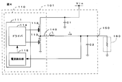
- FIG. 4 is a diagram illustrating an example of a power supply circuit formed by modules.
- the power supply circuit 101 forms a general step-down DC-DC converter and supplies DC power to the load 160.
- the power supply circuit 101 includes an inductor L inserted in series with the power supply unit 110 and the power supply path 140. (Choke coil) and input / output capacitors C1 and C2 that are shunt-connected between the power supply path 140 and the ground, respectively.
- the power supply unit 110 is formed of an IC in which circuit elements for forming the DC-DC converter are formed, and includes a control circuit 111 and switch elements 112 and 113 formed of MOSFETs or the like, and an input capacitor It is connected to an external DC power source Vin via C1.
- the control circuit 111 includes a driver 114 that switches on and off of the switch elements 112 and 113 by PWM driving, and a current detection unit 115 that detects a load power supply current i to the load 160.
- the current detection unit 115 is formed by a general differential amplifier or the like. Switching on and off of the switch elements 112 and 113 is controlled by the driver 114 based on the detection signal of the current detection unit 115. Then, DC power is supplied to the load 160 via the power supply path 140 and the output terminal 150 by feedback control based on the detection signal of the current detection unit 115 in the power supply unit 110.
- the switch element 112 is turned on by the driver 114 and the switch element 113 is turned off, so that the load power supply current i from the DC power supply Vin to the load 160 is turned on. Will increase.
- the load power supply current i increases, the voltage value detected by the current detection unit 115 increases.
- the switch element 112 is turned off by the driver 114.
- the switch element 113 is turned on.
- the switch element 112 When the on / off of the switch elements 112 and 113 is switched by the driver 114, the charged output capacitor C2 starts to be discharged, and the load feeding current i decreases.
- the load power supply current i decreases, the voltage value detected by the current detection unit 115 decreases.
- the switch element 112 When the detected value becomes smaller than a predetermined value, the switch element 112 is turned on by the driver 114 and the switch Element 113 is turned off.
- the inductor L described above is formed by the coil constituted by the coil core 4 and the coil electrode 5 of the module 1, and the input / output capacitors C 1, 9 b are arranged by the two electronic components 9 a, 9 b disposed inside the coil core 4.
- C2 is formed.
- the power supply circuit 101 (power supply unit 110) has been described by taking a general step-down DC-DC converter as an example. However, the power supply circuit 101 may have any known configuration, and the driver 114 Since the detailed configuration and operation of the current detection unit 115 are well known, other detailed description is omitted.
- Module manufacturing method Next, an example of a method for manufacturing the module 1 will be briefly described. First, a plurality of mounting electrodes, via conductors 10 and various wiring electrodes for the electronic components 9a to 9c are formed at predetermined positions on both main surfaces, and a part of the coil electrode 5 is formed on the main surface on the lower surface side. A wiring board 2 on which a plurality of upper wiring patterns 7 to be formed is formed is prepared.
- each of the inner and outer metal pins 6a and 6b and the metal pin 12 for external connection is connected to a predetermined position on each upper wiring pattern 7 on the lower surface of the wiring board 2 using solder or the like.
- both electronic components 9a and 9b are also mounted by soldering or the like in the inner region surrounded by the inner metal pins 6a.
- the coil core 4 is placed at a predetermined position on the lower surface of the wiring board 2, and the lower surface of the wiring board 2 is covered with a resin so as to cover the metal pins 6a, 6b, 12 and the coil core 4 (formation of the insulating layer 3).
- a resin so as to cover the metal pins 6a, 6b, 12 and the coil core 4 (formation of the insulating layer 3).
- an epoxy resin can be used as this resin.
- the lower surface of the insulating layer 3 is polished or ground until the other end of each metal pin 6a, 6b, 12 is exposed.
- each lower wiring pattern 8 and the external electrodes 11 are formed on the lower surface of the insulating layer 3.
- each lower wiring pattern 8 and each external electrode 11 are formed by, for example, forming a base electrode by screen printing using a conductive paste containing Cu or the like, and then applying Cu plating to the base electrode. Can be formed.
- an insulating coating film 13 is formed on the lower surface of the insulating layer 3 by screen printing or the like.
- the insulating coating film 13 can be formed of, for example, polyimide or epoxy resin.
- the electronic component 9c is mounted on the upper surface of the wiring board 2 to complete the module 1.
- a resin layer for sealing the electronic component 9 c may be further provided on the upper surface of the wiring board 2.
- the electronic components 9a and 9b are mounted on the lower surface of the wiring board 2 and disposed in the region inside the coil core 4 in the insulating layer 3, and thus the electronic components 9a and 9b.
- the area of the main surface of the wiring board 2 or the insulating layer 3 is not increased, and the module 1 can be downsized.
- the height H1 of the electronic components 9a and 9b mounted on the lower surface of the wiring board 2 from the lower surface of the wiring board 2 is the height H1 of the electronic component 9c mounted on the upper surface of the wiring board 2 from the upper surface of the wiring board 2. Since the height is higher than the height H2, the height of the module 1 can be reduced as compared with the case where all of the electronic components 9a to 9c are mounted on the upper surface of the wiring board 2.
- the metal pins 6a and 6b have a lower specific resistance than a via conductor or a through-hole conductor formed by filling a via hole with a conductive paste, the resistance value of the coil electrode 5 as a whole can be lowered. . Therefore, for example, the module 1 excellent in coil characteristics such as Q value can be provided.
- FIGS. 5A and 5B are plan views of modules each showing a modification of the coil core. Further, in FIGS. 5A and 5B, only the insulating layer, only the electronic component and the coil core disposed inside the insulating layer are shown, and the other components are not shown.
- the coil core 4 is formed in an annular shape.
- the shape of the coil core 4 can be appropriately changed as long as the shape surrounds a predetermined region.
- the coil core 4a may have a shape in which a part of a rectangular loop shape is cut in a plan view.
- disconnected two places of rectangular loop shape by planar view may be sufficient.
- the present invention is not limited to the above-described embodiments, and various modifications other than those described above can be made without departing from the spirit of the invention.
- the insulating layer 3 may be formed of a ceramic material, for example.
- the case where the DC-DC converter is formed by the module 1 has been described.
- a coil including the coil cores 4, 4 a and 4 b and the coil electrode 5 and other electronic components are provided.
- a different one from the DC-DC converter may be formed.
- the electronic components 9a and 9b arranged inside the coil core 4 are not limited to chip capacitors, but are, for example, chip space, chip resistors, ICs, connectors, and other open space in the coil core 4 area. Can be appropriately changed according to the configuration of the electronic component included in the module.
- all the electronic components 9a to 9c may be arranged in the insulating layer 3.
- the electronic component 9c that has been mounted on the upper surface of the wiring board 2 may be disposed outside (outer peripheral side) of the coil core 4 in plan view. In this way, the area of the module 1 in plan view can be reduced compared to the case where all the electronic components 9a to 9c are arranged outside the coil core 4 in plan view.
- another electronic component may be mounted on the lower surface of the insulating layer 3 (the main surface opposite to the wiring board 2).
- the present invention can be widely applied to various modules including a wiring board, an insulating layer in which a coil core is embedded, a coil electrode wound around the coil core, and an electronic component.
Landscapes
- Engineering & Computer Science (AREA)
- Power Engineering (AREA)
- Microelectronics & Electronic Packaging (AREA)
- Coils Or Transformers For Communication (AREA)
- Manufacturing Cores, Coils, And Magnets (AREA)
Abstract
L'invention vise à obtenir une réduction de la taille d'un module qui est pourvu d'une bobine et d'un composant électronique. Ledit module (1) est pourvu : d'une carte de câblage (2); d'une couche isolante (3) qui est stratifiée sur la surface inférieure de la carte de câblage (2); d'un noyau de bobine annulaire (4) qui est encastré dans la couche isolante (3); d'une électrode de bobine (5) qui est enroulée autour du noyau de bobine (4); de composants électroniques (9a, 9b) qui sont disposés dans une région de la couche isolante (3), ladite région étant comprise à l'intérieur du noyau de bobine (4); et d'un composant électronique (9c) qui est monté sur la surface supérieure de la carte de câblage (2). Grâce à cette configuration, les aires des surfaces principales de la carte de câblage (2) et la couche isolante (3) ne sont pas grandes par comparaison au cas où les composants électroniques (9a, 9b) et (9c) sont montés sur la surface supérieure de la carte de câblage (2), et de ce fait, la taille du module (1) peut être réduite.
Priority Applications (2)
| Application Number | Priority Date | Filing Date | Title |
|---|---|---|---|
| JP2016573245A JP6365696B2 (ja) | 2015-02-06 | 2016-01-08 | モジュール |
| US15/669,187 US10575405B2 (en) | 2015-02-06 | 2017-08-04 | Module |
Applications Claiming Priority (2)
| Application Number | Priority Date | Filing Date | Title |
|---|---|---|---|
| JP2015021776 | 2015-02-06 | ||
| JP2015-021776 | 2015-02-06 |
Related Child Applications (1)
| Application Number | Title | Priority Date | Filing Date |
|---|---|---|---|
| US15/669,187 Continuation US10575405B2 (en) | 2015-02-06 | 2017-08-04 | Module |
Publications (1)
| Publication Number | Publication Date |
|---|---|
| WO2016125531A1 true WO2016125531A1 (fr) | 2016-08-11 |
Family
ID=56563882
Family Applications (1)
| Application Number | Title | Priority Date | Filing Date |
|---|---|---|---|
| PCT/JP2016/050459 Ceased WO2016125531A1 (fr) | 2015-02-06 | 2016-01-08 | Module |
Country Status (3)
| Country | Link |
|---|---|
| US (1) | US10575405B2 (fr) |
| JP (1) | JP6365696B2 (fr) |
| WO (1) | WO2016125531A1 (fr) |
Cited By (2)
| Publication number | Priority date | Publication date | Assignee | Title |
|---|---|---|---|---|
| JP2019138847A (ja) * | 2018-02-14 | 2019-08-22 | 新電元工業株式会社 | ロゴスキーコイル内蔵基板 |
| JP2022067040A (ja) * | 2020-10-19 | 2022-05-02 | ▲創▼一科技(▲長▼沙)有限公司 | 金属粉末コアからなる集積チップインダクタの製造方法 |
Families Citing this family (4)
| Publication number | Priority date | Publication date | Assignee | Title |
|---|---|---|---|---|
| TWI723343B (zh) * | 2019-02-19 | 2021-04-01 | 頎邦科技股份有限公司 | 具立體電感之半導體結構及其製造方法 |
| US11189563B2 (en) * | 2019-08-01 | 2021-11-30 | Nanya Technology Corporation | Semiconductor structure and manufacturing method thereof |
| EP3840547A1 (fr) * | 2019-12-20 | 2021-06-23 | AT & S Austria Technologie & Systemtechnik Aktiengesellschaft | Support de composant à incrustation magnétique intégrée et à structure de bobine intégrée |
| US12482595B2 (en) | 2019-12-20 | 2025-11-25 | At&S Austria Technologie & Systemtechnik Ag | Component carrier with embedded magnetic inlay and integrated coil structure |
Citations (3)
| Publication number | Priority date | Publication date | Assignee | Title |
|---|---|---|---|---|
| JPH10242339A (ja) * | 1996-12-26 | 1998-09-11 | Citizen Electron Co Ltd | Smd型回路装置及びその製造方法 |
| JP2005026249A (ja) * | 2003-06-30 | 2005-01-27 | Mitsuo Ebisawa | トロイダルコイルのコア体 |
| JP2010516056A (ja) * | 2007-01-11 | 2010-05-13 | プラナーマグ インコーポレイテッド | 平面型広帯域トランス |
Family Cites Families (3)
| Publication number | Priority date | Publication date | Assignee | Title |
|---|---|---|---|---|
| US7196607B2 (en) * | 2004-03-26 | 2007-03-27 | Harris Corporation | Embedded toroidal transformers in ceramic substrates |
| US7805891B2 (en) * | 2007-05-18 | 2010-10-05 | Hurricane Harness Corporation | Apparatus and method for securing a roof assembly during a severe wind storm |
| JP2013207149A (ja) | 2012-03-29 | 2013-10-07 | Keihin Corp | トロイダルコイル |
-
2016
- 2016-01-08 WO PCT/JP2016/050459 patent/WO2016125531A1/fr not_active Ceased
- 2016-01-08 JP JP2016573245A patent/JP6365696B2/ja active Active
-
2017
- 2017-08-04 US US15/669,187 patent/US10575405B2/en active Active
Patent Citations (3)
| Publication number | Priority date | Publication date | Assignee | Title |
|---|---|---|---|---|
| JPH10242339A (ja) * | 1996-12-26 | 1998-09-11 | Citizen Electron Co Ltd | Smd型回路装置及びその製造方法 |
| JP2005026249A (ja) * | 2003-06-30 | 2005-01-27 | Mitsuo Ebisawa | トロイダルコイルのコア体 |
| JP2010516056A (ja) * | 2007-01-11 | 2010-05-13 | プラナーマグ インコーポレイテッド | 平面型広帯域トランス |
Cited By (4)
| Publication number | Priority date | Publication date | Assignee | Title |
|---|---|---|---|---|
| JP2019138847A (ja) * | 2018-02-14 | 2019-08-22 | 新電元工業株式会社 | ロゴスキーコイル内蔵基板 |
| JP7109204B2 (ja) | 2018-02-14 | 2022-07-29 | 新電元工業株式会社 | ロゴスキーコイル内蔵基板 |
| JP2022067040A (ja) * | 2020-10-19 | 2022-05-02 | ▲創▼一科技(▲長▼沙)有限公司 | 金属粉末コアからなる集積チップインダクタの製造方法 |
| JP7190527B2 (ja) | 2020-10-19 | 2022-12-15 | ▲創▼一科技(▲長▼沙)有限公司 | 金属粉末コアからなる集積チップインダクタの製造方法 |
Also Published As
| Publication number | Publication date |
|---|---|
| US20170339791A1 (en) | 2017-11-23 |
| JP6365696B2 (ja) | 2018-08-01 |
| JPWO2016125531A1 (ja) | 2017-11-16 |
| US10575405B2 (en) | 2020-02-25 |
Similar Documents
| Publication | Publication Date | Title |
|---|---|---|
| JP6365696B2 (ja) | モジュール | |
| JP5888621B2 (ja) | 複合電子部品及びその実装基板 | |
| US7940531B2 (en) | DC-DC converter | |
| JP5549600B2 (ja) | 平板状コイル付きモジュールの製造方法及び平板状コイル付きモジュール | |
| CN101266868B (zh) | 超小型电力变换装置 | |
| US10790792B2 (en) | LC composite device, processor, and method for manufacturing LC composite device | |
| JP6551256B2 (ja) | コイル部品、コイル部品を内蔵した回路基板、並びに、コイル部品を備える電源回路 | |
| JP2015088720A (ja) | 複合電子部品及びその実装基板 | |
| JP2009246159A (ja) | 多出力磁気誘導素子およびそれを備えた多出力超小型電力変換装置 | |
| JP3649214B2 (ja) | 超小型電力変換装置およびその製造方法 | |
| JP2015079932A (ja) | 複合電子部品及びその実装基板 | |
| KR20160019324A (ko) | 복합 전자부품, 그 실장 기판 및 포장체 | |
| JP2005167468A (ja) | 電子装置および半導体装置 | |
| JP5429649B2 (ja) | インダクタ内蔵部品及びこれを用いたdc−dcコンバータ | |
| KR102016486B1 (ko) | 복합 전자부품 및 그 실장 기판 | |
| CN107077956A (zh) | 线圈部件 | |
| JP2017084961A (ja) | 集積回路素子の実装構造 | |
| JP2006042538A (ja) | 超小型電力変換装置及び磁気デバイス | |
| KR102004794B1 (ko) | 복합 전자부품 및 그 실장 기판 | |
| JP6575312B2 (ja) | Lc複合デバイスおよびプロセッサ | |
| CN206294416U (zh) | 电子零件的安装构造 | |
| CN206293439U (zh) | 集成电路元件的安装构造 | |
| JP2017092170A (ja) | 電子部品の実装構造 | |
| JP2005124271A (ja) | Dc−dcコンバータ |
Legal Events
| Date | Code | Title | Description |
|---|---|---|---|
| 121 | Ep: the epo has been informed by wipo that ep was designated in this application |
Ref document number: 16746362 Country of ref document: EP Kind code of ref document: A1 |
|
| ENP | Entry into the national phase |
Ref document number: 2016573245 Country of ref document: JP Kind code of ref document: A |
|
| NENP | Non-entry into the national phase |
Ref country code: DE |
|
| 122 | Ep: pct application non-entry in european phase |
Ref document number: 16746362 Country of ref document: EP Kind code of ref document: A1 |