WO2016127427A1 - Procédé de traitement pour boîtier de dispositif électronique, boîtier de dispositif électronique et dispositif électronique - Google Patents
Procédé de traitement pour boîtier de dispositif électronique, boîtier de dispositif électronique et dispositif électronique Download PDFInfo
- Publication number
- WO2016127427A1 WO2016127427A1 PCT/CN2015/073096 CN2015073096W WO2016127427A1 WO 2016127427 A1 WO2016127427 A1 WO 2016127427A1 CN 2015073096 W CN2015073096 W CN 2015073096W WO 2016127427 A1 WO2016127427 A1 WO 2016127427A1
- Authority
- WO
- WIPO (PCT)
- Prior art keywords
- partition strip
- electronic device
- metal
- metal layer
- predetermined
- Prior art date
- Legal status (The legal status is an assumption and is not a legal conclusion. Google has not performed a legal analysis and makes no representation as to the accuracy of the status listed.)
- Ceased
Links
Images

Classifications
-
- H—ELECTRICITY
- H05—ELECTRIC TECHNIQUES NOT OTHERWISE PROVIDED FOR
- H05K—PRINTED CIRCUITS; CASINGS OR CONSTRUCTIONAL DETAILS OF ELECTRIC APPARATUS; MANUFACTURE OF ASSEMBLAGES OF ELECTRICAL COMPONENTS
- H05K5/00—Casings, cabinets or drawers for electric apparatus
- H05K5/04—Metal casings
Definitions
- Embodiments of the present invention relate to electronic technologies, and in particular, to a method for processing an electronic device housing, an electronic device housing, and an electronic device.
- the partition is made of a part of the metal casing of the electronic device as a part of the antenna of the electronic device.
- the metal material of the metal casing is generally aluminum or stainless steel, and the surface is anodized or sandblasted.
- the insulating material of the partition strip plastic material, partition strip and metal casing are generally used.
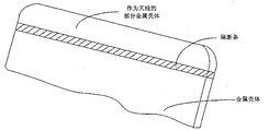
- the width of the partition strip is generally above 0.6mm due to the strength of the plastic material and the performance of the antenna of the electronic device, as shown in Figure 1, due to the material of metal and plastic. Different from the surface treatment, the plastic material of the partition strip can not achieve the metallization effect of the metal shell.
- the existing technical solution is to make the surface of the partition strip as close as possible to the metallization effect by means of plastic material color matching or surface spray paint (the sprayed paint is actually also an organic polymer material). Due to the inherent difference between the two materials, the surface of the plastic material does not have a metallic luster. The color matching or surface coating does not make the surface of the partition strip have a metallized appearance consistent with the metal casing.
- the processing method of the electronic device casing, the electronic device casing and the electronic device provided by the embodiments of the present invention can solve the problem that the surface of the partitioning strip of the electronic device casing cannot have a metallized appearance effect consistent with the metal casing in the prior art.
- an embodiment of the present invention provides a method of processing an electronic device housing, the electronic device housing including a metal housing and a partition strip for blocking the metal housing, the method comprising: at the partition strip The predetermined area of the surface forms a predetermined metal layer, wherein the area of the partition strip surface other than the predetermined area is an insulating area.
- the partition strip is combined with the metal shell by an in-mold injection technique, or the partition strip and the metal shell are nano-formed.
- the technical NMT is combined, or the partition strip is combined with the metal casing by an assembly process.
- the material of the partition strip includes:
- LDS material processed by laser direct structuring technology LDS, plastic material with surface-printed or spray-activated activation component, or acrylonitrile-butadiene-styrene copolymer (English: Acrylonitrile Butadiene Styrene plastic, abbreviation: ABS) material.
- a predetermined metal layer on the predetermined area of the surface of the partition strip includes:
- the metal plated material is subjected to a plating treatment such that the predetermined metal layer is formed on the metal layer.
- the predetermined area on the surface of the partition strip is formed.
- the preset metal layer includes:
- the predetermined metal layer covering the surface of the partition strip over the area other than the predetermined area and the metal layer are removed.
- the method further includes:
- the electronic device housing is energized to prevent the electroless plating process from being performed on the metal housing.
- the method further includes: before performing the electroless plating treatment on the surface of the partition strip, the method further comprises:
- the electronic device housing is energized to prevent the electroless plating process from being performed on the metal housing.
- the predetermined metal layer covering the surface of the partition strip on a region other than the preset area And removing the metal layer includes:
- the predetermined metal layer covering the region other than the predetermined region and the metal layer on the surface of the partition strip are removed by a laser engraving.
- the metal material of the predetermined metal layer is aluminum or nickel.
- an embodiment of the present invention provides an electronic device housing, which is processed by the method as described in the first aspect or any possible implementation thereof.
- an embodiment of the present invention provides an electronic device, comprising the electronic device housing according to the second aspect, wherein the electronic device housing is internally provided with an electronic component of the electronic device.
- the processing method of the electronic device casing, the electronic device casing and the electronic device provided by the embodiment of the present invention include: forming a preset metal layer in a predetermined area on the surface of the partitioning strip of the electronic device casing, the partitioning strip surface except the preset area The area other than the insulation area.
- the partition strip surface of the electronic device casing can have a metallized appearance effect consistent with the metal casing.
- 1 is a schematic structural view of an electronic device housing
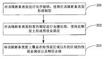
- FIG. 2 is a schematic flow chart 1 of a method for processing an electronic device casing according to an embodiment of the present invention
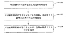
- FIG. 3 is a second schematic flowchart of a method for processing an electronic device casing according to an embodiment of the present invention.
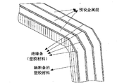
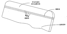
- 4a is a partially enlarged schematic structural view of a partition strip of an electronic device casing processed by the processing method of the electronic device casing provided by the embodiment of the present invention
- 4b is a partially enlarged schematic structural view of an electronic device casing processed by the processing method of the electronic device casing provided by the embodiment of the present invention
- FIG. 5 is a schematic flowchart 3 of a method for processing an electronic device casing according to an embodiment of the present invention.
- In-mold injection technology refers to putting metal parts into a mold and then injecting them. Finally, the metal parts and the plastic parts are combined.
- LDS technology refers to the activation of the catalytic component in the plastic material by laser laser technology on the molded plastic part bracket, and the metal plating layer is formed on the activated plastic surface by electroless plating.
- LDS can provide electrical interconnection function, support component function and support and protection of plastic housing for common plastic components, as well as shielding and antenna functions realized by combining mechanical entities with conductive patterns.
- the LDS material is a modified plastic containing an organic metal composite. After laser irradiation, the organometallic composite releases metal particles.
- NMT technology refers to the technology of combining metal and plastic with nanotechnology. After the metal surface is nano-treated, nano-scale micropores are formed on the metal surface, and the plastic material is injected into the micro-hole and metal. NMT allows metal and plastic to be molded in one piece, which not only balances the appearance of metal. It also simplifies the design of product components.
- ABS material surface plating process is suitable for forming multiple metal layers on the surface of ABS material components, first forming a conductive medium on the surface of the component, and then forming a chemical metal layer (such as chemical copper layer or chemical nickel) by electroless plating.
- the layer is applied to the surface of the plastic component, and then the material properties of the surface of the component are adjusted, and then an electroplated metal layer (such as an electroplated aluminum layer, an electroplated nickel layer or an electroplated chromium layer) is formed on the surface of the chemical metal layer by electrolytic plating.
- the metallization layer has high structural strength and high electrical conductivity, and the component can retain the original characteristics of the material.
- Electroless plating also known as electroless plating or autocatalytic plating, is a plating method in which metal ions in a plating solution are reduced to metal and deposited on the surface of a part without an applied current by means of a suitable reducing agent. Electroless plating is a process of depositing a metal by a controlled redox reaction under the catalysis of a metal.
- electroless plating has been widely used in electronics, valve manufacturing, machinery, petrochemical, automotive, aerospace and other industries.
- the electroless plating treatment may be electroless copper plating, electroless nickel plating, electroless chrome plating, electroless tin plating, electroless gold plating or electroless silver plating, etc., and the actual implementation is selected according to actual needs.
- An embodiment of the present invention provides a method of processing an electronic device housing.
- the electronic device housing includes a metal housing and a partition strip for blocking the metal housing. As shown in FIG. 2, the method includes:
- Step 10 forming a predetermined metal layer on a predetermined area of the surface of the partition strip, wherein the area of the partition strip surface other than the preset area is an insulating area.
- the partition strip and the metal shell may be combined by in-mold molding technology, or the partition strip and the metal shell may be combined by a nano-forming technology NMT, or the partition strip and the metal shell may be further It can be combined by an assembly process.
- the material of the partition strip includes: an LDS material that can be processed by LDS, a plastic material that is surface-printed or sprayed with a laser-activated activation component, or an ABS material.
- the material of the partition strip is an LDS material or a plastic material whose surface is printed or sprayed with a laser-activated activation component, and the electroless plating process is selected as electroless copper plating, as shown in FIG. 3, step 10
- the forming a predetermined metal layer on the predetermined area of the surface of the partition strip may specifically include:
- Step 101 Perform a laser engraving process on a predetermined area of the surface of the partition strip.
- the laser laser engraving process is performed on the preset area of the surface of the partition strip as shown in FIG. 2, and the area outside the preset area in FIG. 2, that is, the width of the insulating area is 0.1-0.2 mm, which is activated by laser engraving.
- the electroless plating function of the area material is set.
- the shape of the partition strip may be a regular linear shape, a ring shape, or other irregular patterns.
- the shape of the partition strip shown in FIG. 2 is merely schematic, and the shape of the partition strip is specifically determined by a technician. The actual demand selection is not limited by the present invention.
- Step 102 Perform electroless copper plating on the preset area after the laser engraving, so that a copper layer is formed on the material corresponding to the preset area.
- Electroless copper plating is a mature technology in the existing application.
- the electroless copper plating on the preset area after the laser engraving treatment is as follows: the copper is reacted by formaldehyde, and the copper is attached to the surface of the preset area after the laser engraving treatment.
- the thickness of the copper layer is required to be 10 um or more.
- the electronic device housing can be energized to block the metal.
- the housing is electroless copper plated.
- the partition strip and the metal shell are combined by an assembly process, the partition strip can be treated separately, and the metal shell is not involved in the electroless copper plating on the predetermined area of the partition strip.
- Step 103 Electroplating the material coated with the copper layer to form a predetermined metal layer on the copper layer.
- the metal material of the metal casing is generally stainless steel or aluminum. If the metal casing is stainless steel, the surface of the metal casing and the predetermined surface of the partition strip are plated with nickel, and the effect of nickel plating is stainless steel. The effect after sand blasting is very close; if the metal shell is aluminum, the metal material of the preset metal layer is also selected as aluminum, and the surface of the copper layer is plated with aluminum by electroplating, and the thickness of the aluminum is generally required to be 0.1 mm or more.
- the electroless copper plating is naturally deposited and adhered to the surface, and the electroplating is forced exchange of electrons by electric current, and the plating layer is dense, and a bright surface effect can be achieved.
- the aluminum layer formed by electroplating the aluminum in the predetermined region is sandblasted or anodized to achieve a uniform metallization effect.
- FIG. 4a is a partially enlarged structural view of the partition strip, wherein the partition strip has four strips of 0.1-0.2 mm width except the predetermined area, and the insulating strip is still a plastic material for blocking the antenna. And the main housing, weakening the antenna coupling effect, achieving the effect equivalent to the complete disconnection, and ensuring the performance of the antenna while realizing the integrated metal effect of the outer casing.
- Figure 4b is electricity A partially enlarged schematic view of the sub-device housing, wherein the dotted line portion is an enlarged insulating tape.
- the metal material of the partition strip is the ABS material as an example, wherein the metal material of the metal shell is aluminum, the metal material of the predetermined metal layer is also selected as aluminum, and the electroless plating is selected as electroless copper plating, as shown in the figure.
- the forming a predetermined metal layer on the predetermined area of the surface of the partitioning strip in the step 10 may specifically include:
- Step 201 Perform electroless copper plating on the surface of the partition strip to form a copper layer on the surface of the partition strip.
- the electronic device housing can be energized to block the metal.
- the housing is electroless copper plated.
- Step 202 Perform a plating process on the copper layer attached to the surface of the partition strip, so that a predetermined metal layer is formed on the copper layer.
- step 103 aluminum is plated on the copper layer attached to the surface of the partition strip.
- Step 203 removing a predetermined metal layer and a copper layer covering the surface of the partition strip on a surface other than the preset area.
- the predetermined metal layer and the copper layer covering the area other than the preset area on the surface of the partition strip may be removed by using a laser engraving.
- step 202 is completely aluminizing the surface of the partition strip, the aluminum layer and the copper layer covering the area other than the predetermined area on the surface of the partition strip are removed by laser laser engraving to make the area Become an insulation zone.
- the aluminum layer formed by electroplating the aluminum in the predetermined region is sandblasted or anodized to achieve a uniform metallization effect.
- FIG. 4a is a partially enlarged structural view of the partition strip, wherein the partition strip has four strips of 0.1-0.2 mm width except the predetermined area, and the insulating strip is still a plastic material for blocking the antenna. And the main housing, weakening the antenna coupling effect, achieving the effect equivalent to the complete disconnection, and ensuring the performance of the antenna while realizing the integrated metal effect of the outer casing.
- Figure 4b is electricity A partially enlarged schematic view of the sub-device housing, wherein the dotted line portion is an enlarged insulating tape.
- a predetermined metal layer is formed on a predetermined area of the surface of the partitioning strip of the electronic device casing, and the surface of the partitioning strip except the predetermined area is an insulating region.
- the partition strip surface of the electronic device casing can have a metallized appearance effect consistent with the metal casing.
- Embodiments of the present invention provide an electronic device housing obtained by the processing method provided by the above method embodiment.
- the surface of the partition strip of the electronic device casing provided by the embodiment of the invention has the same metallization effect as the metal casing.
- the embodiment of the present invention further provides an electronic device, including the electronic device casing provided by the above embodiment, wherein the electronic device casing is internally provided with electronic components of the electronic device.
- the surface of the partition strip of the outer casing of the electronic device provided by the embodiment of the invention has a metallizing effect consistent with the metal casing.
- the disclosed apparatus and method may be implemented in other manners.
- the device embodiments described above are merely illustrative.
- the division of the unit is only a logical function division.
- there may be another division manner for example, multiple units or components may be combined or Can be integrated into another system, or some features can be ignored or not executed.
- the mutual coupling or direct coupling or communication connection shown or discussed may be an indirect coupling or communication connection through some interface, device or unit, and may be in an electrical, mechanical or other form.
- the units described as separate components may or may not be physically separated, and the components displayed as units may or may not be physical units, that is, may be located in one place, or may be distributed to multiple network units. Some or all of the units may be selected according to actual needs to achieve the purpose of the solution of the embodiment.
- each functional unit in each embodiment of the present invention may be integrated into one processing unit, or each unit may exist physically separately, or two or more units may be integrated into one unit.
- the above integrated unit can be implemented in the form of hardware or in the form of hardware plus software functional units.
- the above-described integrated unit implemented in the form of a software functional unit can be stored in a computer readable storage medium.
- the above software functional unit is stored in a storage medium and includes a plurality of instructions for causing a computer device (which may be a personal computer, a server, or a network)
- a device or the like or a processor performs part of the steps of the method of the various embodiments of the present invention.
- the foregoing storage medium includes: a U disk, a mobile hard disk, a read-only memory (ROM), a random access memory (RAM), a magnetic disk, or an optical disk, and the like, which can store program codes. .
- the foregoing program may be stored in a computer readable storage medium, and the program is executed when executed.
- the foregoing steps include the steps of the foregoing method embodiments; and the foregoing storage medium includes: a medium that can store program codes, such as a ROM, a RAM, a magnetic disk, or an optical disk.
Landscapes
- Engineering & Computer Science (AREA)
- Microelectronics & Electronic Packaging (AREA)
- Electroplating Methods And Accessories (AREA)
- Chemically Coating (AREA)
Abstract
L'invention concerne un procédé de traitement pour un boîtier de dispositif électronique, un boîtier de dispositif électronique et un dispositif électronique. Le procédé consiste à : former une couche métallique prédéfinie dans une région prédéfinie sur une surface de bande de séparation d'un boîtier de dispositif électronique, dans lequel procédé une région de la surface de bande de séparation, à l'écart de la région prédéfinie, est une région d'isolation. Au moyen du procédé, une surface de bande de séparation d'un boîtier de dispositif électronique peut présenter le même effet d'apparence de métallisation effet que celui d'un boîtier métallique.
Priority Applications (2)
| Application Number | Priority Date | Filing Date | Title |
|---|---|---|---|
| PCT/CN2015/073096 WO2016127427A1 (fr) | 2015-02-15 | 2015-02-15 | Procédé de traitement pour boîtier de dispositif électronique, boîtier de dispositif électronique et dispositif électronique |
| CN201580003300.8A CN106063395B (zh) | 2015-02-15 | 2015-02-15 | 电子设备外壳的加工方法、电子设备外壳及电子设备 |
Applications Claiming Priority (1)
| Application Number | Priority Date | Filing Date | Title |
|---|---|---|---|
| PCT/CN2015/073096 WO2016127427A1 (fr) | 2015-02-15 | 2015-02-15 | Procédé de traitement pour boîtier de dispositif électronique, boîtier de dispositif électronique et dispositif électronique |
Publications (1)
| Publication Number | Publication Date |
|---|---|
| WO2016127427A1 true WO2016127427A1 (fr) | 2016-08-18 |
Family
ID=56615236
Family Applications (1)
| Application Number | Title | Priority Date | Filing Date |
|---|---|---|---|
| PCT/CN2015/073096 Ceased WO2016127427A1 (fr) | 2015-02-15 | 2015-02-15 | Procédé de traitement pour boîtier de dispositif électronique, boîtier de dispositif électronique et dispositif électronique |
Country Status (2)
| Country | Link |
|---|---|
| CN (1) | CN106063395B (fr) |
| WO (1) | WO2016127427A1 (fr) |
Cited By (5)
| Publication number | Priority date | Publication date | Assignee | Title |
|---|---|---|---|---|
| CN106935965A (zh) * | 2017-03-24 | 2017-07-07 | 苏州胜利精密制造科技股份有限公司 | 一种具有天线装饰功能的壳体及制备工艺 |
| CN107755880A (zh) * | 2017-11-17 | 2018-03-06 | 珠海市魅族科技有限公司 | 镭雕机和壳体的加工方法 |
| WO2019099597A2 (fr) | 2017-11-17 | 2019-05-23 | Merck Sharp & Dohme Corp. | Anticorps spécifiques du transcrit 3 de type immunoglobuline (ilt3) et leurs utilisations |
| WO2021101676A1 (fr) * | 2019-11-22 | 2021-05-27 | Microsoft Technology Licensing, Llc | Systèmes et procédés de fabrication de boîtiers de dispositifs électroniques |
| CN113972488A (zh) * | 2021-09-22 | 2022-01-25 | 上海闻泰电子科技有限公司 | 天线壳体注塑成型方法及天线壳体 |
Families Citing this family (3)
| Publication number | Priority date | Publication date | Assignee | Title |
|---|---|---|---|---|
| CN114737178A (zh) * | 2022-03-28 | 2022-07-12 | 中银金融科技有限公司 | 一种高性能电磁屏蔽胶条的成型方法 |
| CN116180178A (zh) * | 2022-12-22 | 2023-05-30 | 歌尔股份有限公司 | 复合材料及其制备方法、壳体和电子设备 |
| CN116023689A (zh) * | 2022-12-22 | 2023-04-28 | 歌尔股份有限公司 | 复合材料及其制备方法、壳体和电子设备 |
Citations (5)
| Publication number | Priority date | Publication date | Assignee | Title |
|---|---|---|---|---|
| CN101800361A (zh) * | 2010-03-23 | 2010-08-11 | 中兴通讯股份有限公司 | 一种无线设备 |
| CN102142855A (zh) * | 2010-05-27 | 2011-08-03 | 苹果公司 | 用于优化发射的射频信号的位置的壳体结构 |
| CN103510049A (zh) * | 2013-09-22 | 2014-01-15 | 东莞劲胜精密组件股份有限公司 | 一种使塑胶表面具有高金属质感的处理方法 |
| CN103582328A (zh) * | 2012-07-23 | 2014-02-12 | 崇鼎科技有限公司 | 形成金属构件于机壳的方法 |
| CN104066293A (zh) * | 2013-03-21 | 2014-09-24 | 宏达国际电子股份有限公司 | 电子装置机壳与其制作方法 |
Family Cites Families (5)
| Publication number | Priority date | Publication date | Assignee | Title |
|---|---|---|---|---|
| TWI450829B (zh) * | 2008-01-18 | 2014-09-01 | Decorative film for bonding and its manufacturing method | |
| CN101677496A (zh) * | 2008-09-18 | 2010-03-24 | 深圳富泰宏精密工业有限公司 | 壳体及其制作方法 |
| CN102299403A (zh) * | 2010-06-28 | 2011-12-28 | 深圳富泰宏精密工业有限公司 | 电子装置壳体及其制作方法 |
| CN102724840B (zh) * | 2011-03-29 | 2015-03-04 | 富准精密工业(深圳)有限公司 | 壳体及其制造方法 |
| CN102806789A (zh) * | 2011-06-03 | 2012-12-05 | 上海安费诺永亿通讯电子有限公司 | 在绝缘体表面形成金属图案的方法 |
-
2015
- 2015-02-15 WO PCT/CN2015/073096 patent/WO2016127427A1/fr not_active Ceased
- 2015-02-15 CN CN201580003300.8A patent/CN106063395B/zh active Active
Patent Citations (5)
| Publication number | Priority date | Publication date | Assignee | Title |
|---|---|---|---|---|
| CN101800361A (zh) * | 2010-03-23 | 2010-08-11 | 中兴通讯股份有限公司 | 一种无线设备 |
| CN102142855A (zh) * | 2010-05-27 | 2011-08-03 | 苹果公司 | 用于优化发射的射频信号的位置的壳体结构 |
| CN103582328A (zh) * | 2012-07-23 | 2014-02-12 | 崇鼎科技有限公司 | 形成金属构件于机壳的方法 |
| CN104066293A (zh) * | 2013-03-21 | 2014-09-24 | 宏达国际电子股份有限公司 | 电子装置机壳与其制作方法 |
| CN103510049A (zh) * | 2013-09-22 | 2014-01-15 | 东莞劲胜精密组件股份有限公司 | 一种使塑胶表面具有高金属质感的处理方法 |
Cited By (10)
| Publication number | Priority date | Publication date | Assignee | Title |
|---|---|---|---|---|
| CN106935965A (zh) * | 2017-03-24 | 2017-07-07 | 苏州胜利精密制造科技股份有限公司 | 一种具有天线装饰功能的壳体及制备工艺 |
| CN106935965B (zh) * | 2017-03-24 | 2024-03-19 | 苏州胜利精密制造科技股份有限公司 | 一种具有天线装饰功能的壳体及制备工艺 |
| CN107755880A (zh) * | 2017-11-17 | 2018-03-06 | 珠海市魅族科技有限公司 | 镭雕机和壳体的加工方法 |
| WO2019099597A2 (fr) | 2017-11-17 | 2019-05-23 | Merck Sharp & Dohme Corp. | Anticorps spécifiques du transcrit 3 de type immunoglobuline (ilt3) et leurs utilisations |
| US11111297B2 (en) | 2017-11-17 | 2021-09-07 | Merck Sharp & Dohme Corp. | Antibodies specific for immunoglobulin-like transcript 3 (ILT3) and uses thereof |
| US12435133B2 (en) | 2017-11-17 | 2025-10-07 | Merck Sharp & Dohme Llc | Antibodies specific for immunoglobulin-like transcript 3 (ILT3) and uses thereof |
| US12441792B2 (en) | 2017-11-17 | 2025-10-14 | Merck Sharp & Dohme Llc | Antibodies specific for immunoglobulin-like transcript 3 (ILT3) and uses thereof |
| WO2021101676A1 (fr) * | 2019-11-22 | 2021-05-27 | Microsoft Technology Licensing, Llc | Systèmes et procédés de fabrication de boîtiers de dispositifs électroniques |
| US11744058B2 (en) | 2019-11-22 | 2023-08-29 | Microsoft Technology Licensing, Llc | Systems and methods for manufacturing electronic device housings |
| CN113972488A (zh) * | 2021-09-22 | 2022-01-25 | 上海闻泰电子科技有限公司 | 天线壳体注塑成型方法及天线壳体 |
Also Published As
| Publication number | Publication date |
|---|---|
| CN106063395A (zh) | 2016-10-26 |
| CN106063395B (zh) | 2019-06-11 |
Similar Documents
| Publication | Publication Date | Title |
|---|---|---|
| CN106063395B (zh) | 电子设备外壳的加工方法、电子设备外壳及电子设备 | |
| CN104838634B (zh) | 电子设备的主体和便携式电子设备 | |
| TWI445474B (zh) | Manufacturing method of plastic metallized three - dimensional line | |
| CN102892252B (zh) | 三维电路的制造方法 | |
| CN103022638A (zh) | 一种采用激光直接成型技术制作移动终端内置天线的方法 | |
| WO2018228031A1 (fr) | Boîtier, procédé de fabrication associé, et terminal mobile | |
| JP5144682B2 (ja) | 裏面金属化方法 | |
| WO2012018595A2 (fr) | Processus de fabrication de mousses polymère hautement électroconductrices dotées d'un ensemble de compression commandé adapté à être utilisé dans des applications de protecteur d'interférences électromagnétiques | |
| US9112265B2 (en) | Method for manufacturing antenna structure | |
| JP2001200376A (ja) | 電磁波シールド被膜の形成方法 | |
| CN105428780A (zh) | 一种工件制作方法、工件及电子设备 | |
| JP3811272B2 (ja) | 電磁波シールド筐体及びその製造方法 | |
| TWI423751B (zh) | Method of manufacturing three - dimensional circuit | |
| CN114746239A (zh) | 用于制造电子设备壳体的系统和方法 | |
| CN104466368A (zh) | 一种天线的制作方法及电子设备 | |
| CN103972645A (zh) | 移动终端天线及其制作方法 | |
| CN103866300A (zh) | 非金属基材金属化方法 | |
| US20170347444A1 (en) | Manufacturing method of curved circuit board and electronic product | |
| TW200427399A (en) | Method for manufacturing an EMI shielding element | |
| US11326268B2 (en) | Floating metallized element assembly and method of manufacturing thereof | |
| CN105098338A (zh) | 镭雕化镀天线同非导电性真空金属镀膜结合的生产工艺 | |
| JP4355870B2 (ja) | 高難燃性の電磁波シールド用ガスケットおよびその製造方法 | |
| CN102694228A (zh) | 基材上天线的导线接线的形成方法 | |
| CN115666001A (zh) | 精细线路加工方法 | |
| TW201421800A (zh) | 於不導電基材上形成導電圖案的方法 |
Legal Events
| Date | Code | Title | Description |
|---|---|---|---|
| 121 | Ep: the epo has been informed by wipo that ep was designated in this application |
Ref document number: 15881589 Country of ref document: EP Kind code of ref document: A1 |
|
| NENP | Non-entry into the national phase |
Ref country code: DE |
|
| 122 | Ep: pct application non-entry in european phase |
Ref document number: 15881589 Country of ref document: EP Kind code of ref document: A1 |