WO2016136487A1 - Élément de capture d'image, dispositif de capture d'image et dispositif et procédé de fabrication - Google Patents
Élément de capture d'image, dispositif de capture d'image et dispositif et procédé de fabrication Download PDFInfo
- Publication number
- WO2016136487A1 WO2016136487A1 PCT/JP2016/054068 JP2016054068W WO2016136487A1 WO 2016136487 A1 WO2016136487 A1 WO 2016136487A1 JP 2016054068 W JP2016054068 W JP 2016054068W WO 2016136487 A1 WO2016136487 A1 WO 2016136487A1
- Authority
- WO
- WIPO (PCT)
- Prior art keywords
- insulating film
- charge transfer
- gate insulating
- transfer channel
- groove
- Prior art date
- Legal status (The legal status is an assumption and is not a legal conclusion. Google has not performed a legal analysis and makes no representation as to the accuracy of the status listed.)
- Ceased
Links
Images









Classifications
-
- H—ELECTRICITY
- H10—SEMICONDUCTOR DEVICES; ELECTRIC SOLID-STATE DEVICES NOT OTHERWISE PROVIDED FOR
- H10F—INORGANIC SEMICONDUCTOR DEVICES SENSITIVE TO INFRARED RADIATION, LIGHT, ELECTROMAGNETIC RADIATION OF SHORTER WAVELENGTH OR CORPUSCULAR RADIATION
- H10F39/00—Integrated devices, or assemblies of multiple devices, comprising at least one element covered by group H10F30/00, e.g. radiation detectors comprising photodiode arrays
- H10F39/80—Constructional details of image sensors
- H10F39/803—Pixels having integrated switching, control, storage or amplification elements
- H10F39/8037—Pixels having integrated switching, control, storage or amplification elements the integrated elements comprising a transistor
- H10F39/80377—Pixels having integrated switching, control, storage or amplification elements the integrated elements comprising a transistor characterised by the channel of the transistor, e.g. channel having a doping gradient
-
- H—ELECTRICITY
- H10—SEMICONDUCTOR DEVICES; ELECTRIC SOLID-STATE DEVICES NOT OTHERWISE PROVIDED FOR
- H10D—INORGANIC ELECTRIC SEMICONDUCTOR DEVICES
- H10D30/00—Field-effect transistors [FET]
- H10D30/60—Insulated-gate field-effect transistors [IGFET]
- H10D30/63—Vertical IGFETs
-
- H—ELECTRICITY
- H10—SEMICONDUCTOR DEVICES; ELECTRIC SOLID-STATE DEVICES NOT OTHERWISE PROVIDED FOR
- H10D—INORGANIC ELECTRIC SEMICONDUCTOR DEVICES
- H10D62/00—Semiconductor bodies, or regions thereof, of devices having potential barriers
- H10D62/10—Shapes, relative sizes or dispositions of the regions of the semiconductor bodies; Shapes of the semiconductor bodies
- H10D62/17—Semiconductor regions connected to electrodes not carrying current to be rectified, amplified or switched, e.g. channel regions
- H10D62/213—Channel regions of field-effect devices
- H10D62/221—Channel regions of field-effect devices of FETs
- H10D62/235—Channel regions of field-effect devices of FETs of IGFETs
- H10D62/314—Channel regions of field-effect devices of FETs of IGFETs having vertical doping variations
-
- H—ELECTRICITY
- H10—SEMICONDUCTOR DEVICES; ELECTRIC SOLID-STATE DEVICES NOT OTHERWISE PROVIDED FOR
- H10D—INORGANIC ELECTRIC SEMICONDUCTOR DEVICES
- H10D64/00—Electrodes of devices having potential barriers
- H10D64/20—Electrodes characterised by their shapes, relative sizes or dispositions
- H10D64/27—Electrodes not carrying the current to be rectified, amplified, oscillated or switched, e.g. gates
- H10D64/311—Gate electrodes for field-effect devices
- H10D64/411—Gate electrodes for field-effect devices for FETs
- H10D64/511—Gate electrodes for field-effect devices for FETs for IGFETs
- H10D64/512—Disposition of the gate electrodes, e.g. buried gates
- H10D64/513—Disposition of the gate electrodes, e.g. buried gates within recesses in the substrate, e.g. trench gates, groove gates or buried gates
-
- H—ELECTRICITY
- H10—SEMICONDUCTOR DEVICES; ELECTRIC SOLID-STATE DEVICES NOT OTHERWISE PROVIDED FOR
- H10D—INORGANIC ELECTRIC SEMICONDUCTOR DEVICES
- H10D64/00—Electrodes of devices having potential barriers
- H10D64/20—Electrodes characterised by their shapes, relative sizes or dispositions
- H10D64/27—Electrodes not carrying the current to be rectified, amplified, oscillated or switched, e.g. gates
- H10D64/311—Gate electrodes for field-effect devices
- H10D64/411—Gate electrodes for field-effect devices for FETs
- H10D64/511—Gate electrodes for field-effect devices for FETs for IGFETs
- H10D64/514—Gate electrodes for field-effect devices for FETs for IGFETs characterised by the insulating layers
- H10D64/516—Gate electrodes for field-effect devices for FETs for IGFETs characterised by the insulating layers the thicknesses being non-uniform
-
- H—ELECTRICITY
- H10—SEMICONDUCTOR DEVICES; ELECTRIC SOLID-STATE DEVICES NOT OTHERWISE PROVIDED FOR
- H10F—INORGANIC SEMICONDUCTOR DEVICES SENSITIVE TO INFRARED RADIATION, LIGHT, ELECTROMAGNETIC RADIATION OF SHORTER WAVELENGTH OR CORPUSCULAR RADIATION
- H10F39/00—Integrated devices, or assemblies of multiple devices, comprising at least one element covered by group H10F30/00, e.g. radiation detectors comprising photodiode arrays
- H10F39/011—Manufacture or treatment of image sensors covered by group H10F39/12
- H10F39/014—Manufacture or treatment of image sensors covered by group H10F39/12 of CMOS image sensors
-
- H—ELECTRICITY
- H10—SEMICONDUCTOR DEVICES; ELECTRIC SOLID-STATE DEVICES NOT OTHERWISE PROVIDED FOR
- H10F—INORGANIC SEMICONDUCTOR DEVICES SENSITIVE TO INFRARED RADIATION, LIGHT, ELECTROMAGNETIC RADIATION OF SHORTER WAVELENGTH OR CORPUSCULAR RADIATION
- H10F39/00—Integrated devices, or assemblies of multiple devices, comprising at least one element covered by group H10F30/00, e.g. radiation detectors comprising photodiode arrays
- H10F39/10—Integrated devices
- H10F39/12—Image sensors
Definitions
- the present technology relates to an imaging element, an imaging apparatus, and a manufacturing apparatus and method, and more particularly, to an imaging element, an imaging apparatus, and a manufacturing apparatus and method that make it easier to transfer charges.
- Patent Document 1 an image sensor that reads a signal photoelectrically converted by a photoelectric conversion unit with a vertical transistor has been considered (see, for example, Patent Document 1).
- This technology has been proposed in view of such a situation, and aims to make it easier to transfer charges.
- One aspect of the present technology is an imaging device including a vertical transistor having a potential gradient in at least a part of a charge transfer channel that transfers charges of a photoelectric conversion unit.
- the potential may have a gradient that becomes deeper toward the charge transfer destination in the charge transfer direction in the charge transfer channel.
- the charge transfer channel is a first conductivity type charge transfer channel that transfers a charge of the second conductivity type photoelectric conversion unit formed in the first conductivity type semiconductor, and includes a charge transfer channel and a gate electrode.
- the gate insulating film formed therebetween may be formed so that the film thickness gradually decreases toward the charge transfer destination.
- the charge transfer channel is a first conductivity type charge transfer channel that transfers a charge of the second conductivity type photoelectric conversion unit formed in the first conductivity type semiconductor, and includes a charge transfer channel and a gate electrode.
- the gate insulating film formed therebetween may be formed so that the film thickness decreases stepwise toward the charge transfer destination.
- the charge transfer channel is a first conductivity type charge transfer channel that transfers the charge of the second conductivity type photoelectric conversion unit formed in the first conductivity type semiconductor, and the charge transfer channel is the charge transfer channel.
- the impurity concentration can be reduced toward the transfer destination.
- the charge transfer channel is a second conductivity type charge transfer channel that transfers charges of the second conductivity type of the photoelectric conversion unit formed in the first conductivity type semiconductor, and includes a charge transfer channel and a gate electrode.
- the gate insulating film formed therebetween may be formed so that the film thickness gradually increases toward the charge transfer destination.
- the charge transfer channel is a second conductivity type charge transfer channel that transfers charges of the second conductivity type of the photoelectric conversion unit formed in the first conductivity type semiconductor, and includes a charge transfer channel and a gate electrode.
- the gate insulating film formed therebetween may be formed so that the film thickness increases stepwise toward the charge transfer destination.
- the charge transfer channel is a second conductivity type charge transfer channel that transfers charges of the second conductivity type photoelectric conversion unit formed in the first conductivity type semiconductor, and the charge transfer channel is the charge transfer channel.
- the impurity concentration can be increased toward the transfer destination.
- the potential may have a gradient in the direction of rotation along the gate electrode in the charge transfer channel.
- the film thickness of the gate insulating film formed between the charge transfer channel and the gate electrode can be changed in the rotation direction.
- the impurity concentration of the charge transfer channel can be changed in the rotation direction.
- an image sensor including a vertical transistor having a potential gradient in at least a part of a charge transfer channel that transfers charges of a photoelectric conversion unit, and image processing of captured image data obtained by the image sensor And an image processing unit.
- Still another aspect of the present technology is a manufacturing apparatus that manufactures an imaging element, and a vertical transistor that manufactures a vertical transistor having a potential gradient in at least a part of a charge transfer channel that transfers charges of a photoelectric conversion unit. It is a manufacturing apparatus provided with a manufacturing part.
- the vertical transistor manufacturing unit includes: an etching unit that etches a semiconductor substrate to form a groove; a conductive impurity implantation unit that implants a conductive impurity into the groove formed by the etching unit; and a layer in the groove
- a gate insulating film forming portion for forming a gate insulating film with a thickness according to the gate insulating film, a gate insulating film removing portion for removing the gate insulating film formed by the gate insulating film forming portion to a depth corresponding to the hierarchy,
- the vertical transistor manufacturing unit includes: an etching unit that etches a semiconductor substrate to form a groove; a conductive impurity implantation that implants a conductive impurity into the groove formed by the etching unit; and a gate that is formed in the groove.
- a gate insulating film forming portion for forming an insulating film; a gate insulating film processing portion for forming a mesa-shaped groove in the gate insulating film formed by the gate insulating film forming portion; and the gate insulating film processing portion.
- a gate electrode forming portion for forming a gate electrode in the mesa groove.
- the vertical transistor manufacturing unit includes an etching unit that etches a semiconductor substrate to form a groove, a conductive impurity implantation unit that implants conductive impurities into the groove formed by the etching unit, and the etching unit.
- a non-conductive impurity implanted portion for implanting a non-conductive impurity into the formed trench at a concentration corresponding to a depth; a gate insulating film forming portion for forming a gate insulating film in the trench; and the gate insulating film And a gate electrode forming portion for forming a gate electrode in the groove formed in the step.
- the vertical transistor manufacturing unit includes: an etching unit that etches a semiconductor substrate to form a groove; and a conductive impurity that implants a conductive impurity into the groove formed by the etching unit at a concentration according to a depth.
- An implantation part, a gate insulating film forming part for forming a gate insulating film in the groove part, and a gate electrode forming part for forming a gate electrode in the groove part formed in the gate insulating film can be provided.
- the vertical transistor manufacturing unit includes: an etching unit that etches a semiconductor substrate to form a groove; a conductive impurity implantation that implants a conductive impurity into the groove formed by the etching unit; and a gate that is formed in the groove.
- a groove portion so that a film thickness of the gate insulating film changes in a rotation direction along the gate electrode between the gate insulating film forming portion for forming an insulating film and the gate insulating film formed by the gate insulating film forming portion; And a gate electrode forming portion for forming the gate electrode in the groove formed by the gate insulating film processing portion.
- the vertical transistor manufacturing unit includes an etching unit that etches a semiconductor substrate to form a groove portion, a conductive impurity in the groove portion formed by the etching portion, and a position in a rotational direction along the gate electrode.
- a conductivity type impurity implantation portion implanted at a concentration; a gate insulating film forming portion for forming a gate insulating film in the groove portion; and a gate electrode forming portion for forming a gate electrode in the groove portion formed in the gate insulating film. Can do.
- Still another aspect of the present technology is also a manufacturing method of a manufacturing apparatus for manufacturing an imaging device, in which a vertical transistor having a potential gradient in at least a part of a charge transfer channel that transfers charges of a photoelectric conversion unit is provided. It is a manufacturing method to manufacture.
- a vertical transistor having a gradient in potential is provided in at least a part of the charge transfer channel that transfers the charge of the photoelectric conversion unit.
- an image sensor including a vertical transistor having a potential gradient in at least a part of a charge transfer channel that transfers charges of a photoelectric conversion unit, and captured image data obtained by the image sensor And an image processing unit for processing.
- a vertical transistor having a potential gradient in at least a part of a charge transfer channel that transfers charges of a photoelectric conversion unit is manufactured.
- the subject can be imaged.
- it is possible to more easily transfer charges.
- First Embodiment> ⁇ Image sensor with vertical transistor> Conventionally, for example, an image sensor that reads a signal photoelectrically converted by a photoelectric conversion unit with a vertical transistor, such as an image sensor described in Patent Document 1, has been considered.
- a vertical transistor is used as a transfer transistor that controls reading of charges from the photoelectric conversion unit, and the potential of the vertical transistor has a gradient in at least a part of the charge transfer channel that transfers charges.
- FIG. 1 is a cross-sectional view illustrating a main configuration example of a pixel region of an image sensor which is an embodiment of an imaging element to which the present technology is applied.
- An image sensor 100 illustrated in FIG. 1 is a backside illumination type CMOS (Complementary Metal Oxide Semiconductor) image sensor that captures an image of a subject and obtains a captured image as an electrical signal.
- the image sensor 100 has a pixel region composed of a plurality of pixels arranged in a planar shape such as an array. Incident light is photoelectrically converted in each pixel of the pixel region, and a pixel signal of a captured image is obtained.
- CMOS Complementary Metal Oxide Semiconductor
- FIG. 1 an example of a laminated structure of a part of such a pixel region of the image sensor 100 is shown as a cross-sectional view.
- a laminated structure is schematically shown.
- configurations that are not used in the description of the present technology are simplified or omitted.
- the image sensor 100 includes a semiconductor substrate layer 110.
- the semiconductor substrate layer 110 includes, for example, a first conductivity type (for example, p-type) semiconductor substrate 111 and various configurations formed on the semiconductor substrate 111.
- An image sensor 100 shown in FIG. 1 is a backside illumination type image sensor.
- a photoelectric conversion unit for example, a photodiode 112 is formed.
- the photoelectric conversion unit 112 is formed of, for example, a second conductivity type (for example, n-type), photoelectrically converts incident light incident from the back side of the semiconductor substrate (that is, the upper side in the figure), and converts the obtained charge into accumulate.
- a second conductivity type for example, n-type
- a floating diffusion layer 114 is also formed on the semiconductor substrate 111.
- the floating diffusion layer 114 is formed on the front side of the semiconductor substrate 111, and is formed of, for example, a second conductivity type (for example, n + type).
- the floating diffusion layer 114 accumulates charges transferred from the organic photoelectric conversion film 142 described later.
- the insulating film 115 is formed so as to penetrate the semiconductor substrate 111 in the depth direction.
- a transfer transistor 120 is also formed on the semiconductor substrate 111.
- the transfer transistor 120 is a transistor that controls the transfer of charges accumulated in the photoelectric conversion unit 112 to the floating diffusion layer 124, and is formed as a vertical transistor.
- the transfer transistor 120 has a gate portion formed so as to reach the photoelectric conversion portion 112 from the front side of the semiconductor substrate 111.
- the photoelectric conversion unit 112 is formed as the source of such a transfer transistor 120.
- the transfer transistor 120 includes, for example, a charge transfer channel 121, a gate insulating film 122, a gate electrode 123, and a floating diffusion layer 124. Of course, configurations other than these may be formed on the semiconductor substrate 111.
- the charge transfer channel 121 has a configuration of a gate portion of the transfer transistor 120, and is formed in, for example, a first conductivity type (for example, p + type).
- the charge transfer channel 121 is connected to both the photoelectric conversion unit 112 and the floating diffusion layer 124.
- the charge of the photoelectric conversion unit 112 is transmitted to the floating diffusion layer 124 via the charge transfer channel 121.
- the gate insulating film 122 is formed inside the charge transfer channel 121, is formed of an insulator, and is a layer that electrically insulates the charge transfer channel 121 and the gate electrode 123 from each other.
- the gate electrode 123 is an electrode to which a gate potential is applied, and is formed inside the gate insulating film 122.
- the gate electrode 123 is formed of a conductor such as metal.
- the floating diffusion layer 124 is formed on the front side of the semiconductor substrate 111.
- the floating diffusion layer 124 is formed of, for example, a second conductivity type (for example, n + type).
- the floating diffusion layer 124 is formed as the drain of the transfer transistor 120.
- the floating diffusion layer 124 accumulates charges transferred from the photoelectric conversion unit 112.
- a wiring layer 130 is formed on the surface side of the semiconductor substrate layer 110.
- a wiring interlayer film 131 and wirings such as the wiring 132 and the wiring 133 are formed.
- the wiring interlayer film 131 is formed of an insulator and is a layer that electrically insulates wirings made of a conductor such as metal.
- the wiring 132 and the wiring 133 are examples of wiring formed in the wiring layer 130, and actually, wiring other than the wiring 132 and the wiring 133 is also formed in the wiring layer 130.
- the gate electrode 123 is connected to a wiring (control line or the like) not shown through a contact or the like (not shown).
- the gate electrode 123 has a potential corresponding to a signal supplied via the control line (an electric field corresponding to the signal is applied to the charge transfer channel 121).
- the floating diffusion layer 124 is connected to a wiring (not shown) via, for example, a contact (not shown).
- the floating diffusion layer 114 is connected to a wiring (not shown) via, for example, a contact (not shown).
- the charges accumulated in the floating diffusion layer 114 and the floating diffusion layer 124 are supplied to, for example, a gate of an amplification transistor (not shown) through the wiring.
- an insulating film 141 and an organic photoelectric conversion film 142 are stacked.
- a lower transparent electrode 143 is formed on the surface side of the organic photoelectric conversion film 142 in the vicinity of the photoelectric conversion unit 112.
- An upper transparent electrode 144 is formed on the back side of the organic photoelectric conversion film 142.
- the lower transparent electrode 143 is connected to the wiring 133 through a through electrode 145 formed inside the insulating film 115.
- the floating diffusion layer 114 is connected to the wiring 133 through the contact 146. That is, the organic photoelectric conversion film 142 is connected to the floating diffusion layer 114 via the lower transparent electrode 143, the through electrode 145, the wiring 133, and the contact 146.
- the charge obtained by photoelectric conversion of incident light in the organic photoelectric conversion film 142 is supplied to the floating diffusion layer 114 via the lower transparent electrode 143, the through electrode 145, the wiring 133, and the contact 146.
- a passivation layer 151 is formed on the back side of the upper transparent electrode 144.
- the passivation layer 151 is formed of SiN or the like, for example, and protects each layer (for example, the upper transparent electrode 144 and the like) on the surface side of the passivation layer 151.
- an on-chip lens 152 for condensing incident light incident on each pixel on the photoelectric conversion unit 112 or the like is formed.
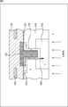
- ⁇ Potential gradient in charge transfer direction> In the image sensor 100 having the pixels configured as described above, for example, as shown in FIG. 2, the charge transfer direction in the charge transfer channel 121 (opposite to the direction of the arrow 161 in FIG. 2) is directed toward the charge transfer destination.
- a potential gradient may be formed so as to be deeper.
- the transfer transistor 120 is a vertical transistor, as shown in FIG. 2, for example, in the portion corresponding to the side wall portion of the gate electrode 123 of the charge transfer channel 121, the charge transfer direction is the same as that of the semiconductor substrate.
- the depth direction is 111 (the direction from the bottom to the top in the figure).
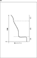
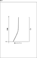
- FIG. 3 shows an example of the potential distribution in the direction indicated by the arrow 161 directed from the floating diffusion layer 124 of FIG. 2 to the photoelectric conversion unit 112 via the charge transfer channel 121.
- the horizontal axis indicates each position indicated by the arrow 161
- the vertical axis indicates the potential depth.
- the potential of the charge transfer channel 121 becomes deeper toward the floating diffusion layer 124 along the arrow 161. That is, the potential has a gradient in at least a part of the charge transfer channel 121.
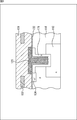
- the gate insulating film may be formed so that its thickness gradually decreases toward the charge transfer destination.
- the gate insulating film 122 may be formed so that the film thickness gradually decreases toward the charge transfer destination (floating diffusion layer 124).
- the gate electrode 123 is formed so as to gradually become thicker toward the charge transfer destination (formed so as to become gradually thinner toward the back surface side in the depth direction of the semiconductor substrate 111. Accordingly, the thickness of the gate insulating film 122 is gradually reduced toward the charge transfer destination.
- the electric field applied to the charge transfer channel 121 can be strengthened as it is closer to the floating diffusion layer 124. Therefore, in the charge transfer channel 121 (particularly, the portion corresponding to the side wall portion of the gate electrode 123 of the charge transfer channel 121), the potential becomes deeper as it approaches the floating diffusion layer 124 as in the example of FIG. can do. In this way, charge transfer from the photoelectric conversion unit 112 to the floating diffusion layer 124 can be facilitated.
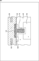
- the gate insulating film may be formed so as to be thin in a stepped manner toward the charge transfer destination.
- the gate insulating film 122 may be formed so that the thickness thereof decreases in a stepped manner toward the charge transfer destination (floating diffusion layer 124).
- the gate electrode 123 is formed so as to increase in a staircase pattern toward the charge transfer destination (in a depth direction of the semiconductor substrate 111, it decreases in a staircase pattern toward the back surface side. Accordingly, the thickness of the gate insulating film 122 is reduced stepwise toward the charge transfer destination.
- the electric field applied to the charge transfer channel 121 can be strengthened as it is closer to the floating diffusion layer 124. Therefore, in the charge transfer channel 121 (particularly, the portion corresponding to the side wall portion of the gate electrode 123 of the charge transfer channel 121), the potential becomes deeper as it approaches the floating diffusion layer 124 as in the example of FIG. can do. In this way, charge transfer from the photoelectric conversion unit 112 to the floating diffusion layer 124 can be facilitated.
- the charge transfer channel of the transfer transistor may be formed of the second conductivity type (for example, n-type).
- the charge transfer channel 171 of the transfer transistor 120 may be formed of the second conductivity type (for example, n-type).
- a charge transfer channel 171 is formed instead of the charge transfer channel 121.
- the charge transfer channel 171 has a configuration of a gate portion of the transfer transistor 120 and is formed, for example, in the second conductivity type (for example, n-type).
- the charge transfer channel 171 is connected to both the photoelectric conversion unit 112 and the floating diffusion layer 124. By applying an electric field to the charge transfer channel 171 (according to the potential of the gate electrode 123), the charge of the photoelectric conversion unit 112 is transmitted to the floating diffusion layer 124 via the charge transfer channel 171.
- the gate insulating film may be formed so that its thickness gradually increases toward the charge transfer destination.
- the gate insulating film 122 may be formed so that the film thickness gradually increases toward the charge transfer destination (floating diffusion layer 124).
- the gate electrode 123 is formed so as to become gradually thinner toward the charge transfer destination (formed so as to become gradually thicker toward the back surface side in the depth direction of the semiconductor substrate 111). Accordingly, the thickness of the gate insulating film 122 gradually increases toward the charge transfer destination.
- the electric field applied to the charge transfer channel 171 can be strengthened as it is closer to the floating diffusion layer 124. Therefore, in the charge transfer channel 171 (particularly, the portion corresponding to the side wall portion of the gate electrode 123 of the charge transfer channel 171), the potential becomes deeper as it approaches the floating diffusion layer 124 as in the example of FIG. can do. In this way, charge transfer from the photoelectric conversion unit 112 to the floating diffusion layer 124 can be facilitated.
- the gate insulating film may be formed so as to increase in a stepped manner toward the charge transfer destination.
- the gate insulating film 122 may be formed so that the thickness thereof increases stepwise toward the charge transfer destination (floating diffusion layer 124).
- the gate electrode 123 is formed to be thin in a staircase pattern toward the charge transfer destination (in a depth direction of the semiconductor substrate 111, it is thickened in a staircase pattern toward the back surface side. Accordingly, the thickness of the gate insulating film 122 is increased stepwise toward the charge transfer destination.
- the electric field applied to the charge transfer channel 171 can be strengthened as it is closer to the floating diffusion layer 124. Therefore, in the charge transfer channel 171 (particularly, the portion corresponding to the side wall portion of the gate electrode 123 of the charge transfer channel 171), the potential becomes deeper as it approaches the floating diffusion layer 124 as in the example of FIG. can do. In this way, charge transfer from the photoelectric conversion unit 112 to the floating diffusion layer 124 can be facilitated.
- the charge transfer channel of the transfer transistor is formed of the first conductivity type (for example, p-type)
- the charge transfer channel is formed so that the impurity concentration decreases toward the charge transfer destination. It may be.
- the concentration of the impurity injected into the charge transfer channel 121 may be reduced toward the charge transfer destination (floating diffusion layer 124).
- the concentration of the impurity implanted into the charge transfer channel 121 decreases in a staircase pattern toward the charge transfer destination (floating diffusion layer 124). That is, the impurity concentration is charge transfer channel 121-1 (p + )> charge transfer channel 121-2 (p)> charge transfer channel 121-3 (p ⁇ ).
- the potential of the charge transfer channel 121 can be made deeper as it approaches the floating diffusion layer 124 as in the example of FIG. In this way, charge transfer from the photoelectric conversion unit 112 to the floating diffusion layer 124 can be facilitated.
- the concentration of the impurity injected into the charge transfer channel 121 may be gradually reduced toward the charge transfer destination (floating diffusion layer 124).
- the impurity concentration may be controlled similarly when the charge transfer channel is of the second conductivity type (for example, n-type).
- the concentration of impurities injected into the second conductivity type (for example, n-type) charge transfer channel 171 may be increased toward the charge transfer destination (floating diffusion layer 124).
- the impurity concentration may be increased stepwise toward the charge transfer destination (floating diffusion layer 124) or gradually increased toward the charge transfer destination (floating diffusion layer 124). It may be.
- a potential gradient may be formed in the rotation direction along the gate electrode in the charge transfer channel.
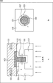
- FIG. 9B shows a horizontal sectional view taken along the dotted line 181 of the gate portion of the transfer transistor 120 shown in FIG. 9A.
- An arrow 182 shown in FIG. 9B indicates the direction of rotation around the gate electrode 123 along the gate electrode 123 in the charge transfer channel 121 of the gate portion.
- FIG. 10 An example of the potential distribution in the direction indicated by the arrow 182 is shown in FIG.
- the horizontal axis indicates each position of the arrow 182, and the vertical axis indicates the potential depth.
- the potential of the charge transfer channel 121 changes along this arrow 182. That is, the potential of the charge transfer channel 121 has a gradient in the direction of the arrow 182 in at least a part of the direction of the arrow 182.
- the thickness of the gate insulating film may be changed in the rotation direction along the gate electrode. That is, the thickness of the gate insulating film 122 may change (have a bias) in the rotation direction indicated by the arrow 182 described above.
- the gate insulating film 122 may have a different film thickness (thicker or thinner than the other portions) in a part of the rotation direction indicated by the arrow 182 described above.
- the thickness of the gate insulating film 122 is increased in the rotation direction indicated by the arrow 182. You may make it produce bias.
- the gate electrode 123 has a cross-sectional shape different from the cross-sectional shape of the gate insulating film 122, whereby the gate insulating film 122 is rotated in the rotation direction indicated by the arrow 182. You may make it produce the nonuniformity of a film thickness.
- the change (bias) of the film thickness in the rotation direction may be gradual or may be stepped.
- the charge transfer channel of the transfer transistor may be formed so that the impurity concentration changes in the rotation direction along the gate electrode in the charge transfer channel.
- the concentration of the impurity injected into the charge transfer channel 121 may change in the rotation direction (arrow 182) along the gate electrode.
- the concentration of the impurity injected into the charge transfer channel 121 is reduced stepwise toward the charge transfer destination (floating diffusion layer 124). That is, the impurity concentration is charge transfer channel 121-1 (p +)> charge transfer channel 121-2 (p)> charge transfer channel 121-3 (p-).
- the charges are concentrated on the low potential portion of the charge transfer channel 121 and transferred from the photoelectric conversion unit 112 to the floating diffusion layer 124. This makes it easier to transfer charges from the photoelectric conversion unit 112 to the floating diffusion layer 124.
- concentration of the impurity injected into the charge transfer channel 121 may be gradually decreased along the arrow 182.
- the thickness of the gate insulating film 122 and the concentration of impurities may be changed in the rotation direction along the gate electrode.
- the charge transfer channel 171 may be provided instead of the charge transfer channel 121.
- the thickness of the gate insulating film 122 and the impurities The concentration may be changed in the direction of rotation along the gate electrode.
- the charges are concentrated on the low potential portion of the charge transfer channel 121 and transferred from the photoelectric conversion unit 112 to the floating diffusion layer 124. . This makes it easier to transfer charges from the photoelectric conversion unit 112 to the floating diffusion layer 124.
- Second Embodiment> ⁇ Manufacturing equipment> Next, the manufacture of the image sensor 100 as described above will be described.
- FIG. 12 is a main configuration example of a manufacturing apparatus that manufactures an image sensor 100 that is an embodiment of an imaging device to which the present technology is applied (a manufacturing apparatus that is an embodiment of a manufacturing apparatus to which the present technology is applied).
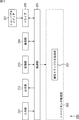
- FIG. A manufacturing apparatus 200 illustrated in FIG. 12 includes a control unit 201 and an image sensor manufacturing unit 202.
- the control unit 201 includes, for example, a CPU (Central Processing Unit), a ROM (Read Only Memory), a RAM (Random Access Memory), and the like, and controls each unit of the image sensor manufacturing unit 202 and relates to the manufacture of the image sensor 100. Perform control processing.
- the CPU of the control unit 201 executes various processes according to programs stored in the ROM. Further, the CPU executes various processes according to programs loaded from the storage unit 213 to the RAM.
- the RAM also appropriately stores data necessary for the CPU to execute various processes.
- the image sensor manufacturing unit 202 is controlled by the control unit 201 to perform processing related to manufacturing of the image sensor 100. That is, in practice, the image sensor manufacturing unit 202 performs processing relating to all processes for manufacturing the image sensor 100. For example, the image sensor manufacturing unit 202 forms each configuration of the semiconductor substrate layer 110 and the wiring layer 130 or forms a configuration on the back side of the semiconductor substrate layer 110 (such as the insulating film 141 to the on-chip lens 152). . However, in the following, for convenience of explanation, only the part relating to the manufacture of the gate part of the transfer transistor 120 will be described.
- the image sensor manufacturing unit 202 includes, for example, a vertical transistor manufacturing unit 231.
- the vertical transistor manufacturing unit 231 performs processing related to the manufacture of the transfer transistor 120 which is a vertical transistor.
- the manufacturing apparatus 200 includes an input unit 211, an output unit 212, a storage unit 213, a communication unit 214, and a drive 215.
- the input unit 211 includes a keyboard, a mouse, a touch panel, an external input terminal, and the like, and receives user instructions and input of information from the outside, and supplies them to the control unit 201.
- the output unit 212 includes a display such as a CRT (Cathode Ray Tube) display or an LCD (Liquid Crystal Display), a speaker, an external output terminal, and the like.
- Various types of information supplied from the control unit 201 can be displayed as images, sounds, or analog. Output as a signal or digital data.
- the storage unit 213 includes an arbitrary storage medium such as a flash memory, an SSD (Solid State Drive), and a hard disk, for example, stores information supplied from the control unit 201, or stores information according to a request from the control unit 201. Read and supply information.
- an arbitrary storage medium such as a flash memory, an SSD (Solid State Drive), and a hard disk, for example, stores information supplied from the control unit 201, or stores information according to a request from the control unit 201. Read and supply information.
- the communication unit 214 includes, for example, a wired LAN (Local Area Network), a wireless LAN interface, a modem, and the like, and performs communication processing with an external device via a network including the Internet. For example, the communication unit 214 transmits information supplied from the control unit 201 to the communication partner, or supplies information received from the communication partner to the control unit 201.
- a wired LAN Local Area Network
- a wireless LAN interface Wireless Local Area Network
- modem Wireless Local Area Network
- the communication unit 214 transmits information supplied from the control unit 201 to the communication partner, or supplies information received from the communication partner to the control unit 201.
- the drive 215 is connected to the control unit 201 as necessary. Then, for example, a removable medium 221 such as a magnetic disk, an optical disk, a magneto-optical disk, or a semiconductor memory is appropriately attached to the drive 215. Then, the computer program read from the removable medium 221 via the drive 215 is installed in the storage unit 213 as necessary.
- a removable medium 221 such as a magnetic disk, an optical disk, a magneto-optical disk, or a semiconductor memory is appropriately attached to the drive 215. Then, the computer program read from the removable medium 221 via the drive 215 is installed in the storage unit 213 as necessary.
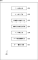
- FIG. 13 is a block diagram illustrating a configuration example of a main processing unit that performs processing related to manufacturing of the gate portion of the transfer transistor 120 included in the vertical transistor manufacturing unit 231.
- the vertical transistor manufacturing unit 231 includes a mask forming unit 241, an etching unit 242, a conductive impurity implantation unit 243, a mask removing unit 244, a gate insulating film deposition unit 245, and a gate insulating film processing unit. 246 and a gate electrode formation portion 247.
- the mask forming unit 241 performs processing related to mask formation.
- the etching unit 242 performs processing related to etching of the semiconductor substrate 111 and the like.
- the conductive impurity implantation unit 243 performs processing related to the implantation of conductive impurities.
- the mask removal unit 244 performs processing related to mask removal.
- the gate insulating film deposition part 245 performs processing related to the formation of the gate insulating film 122.
- the gate insulating film processing unit 246 performs processing related to processing of the gate insulating film 122.
- the gate electrode formation portion 247 performs processing related to formation of the gate electrode.
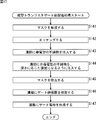
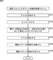
- the vertical transistor manufacturing unit 231 can manufacture the gate units of the examples described with reference to FIGS. 4 to 7, for example. That is, the image sensor manufacturing unit 202 can manufacture the image sensor 100 including the transfer transistor 120 as in each example described with reference to FIGS.
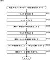
- the mask forming part 241 forms the position (for example, the surface of the photoelectric conversion part 112) where the gate part of the transfer transistor 120 is formed from the surface side of the semiconductor substrate 111 in step S101.
- a mask for forming a groove is formed on the side.
- step S102 the etching unit 242 etches the semiconductor substrate 111 according to the mask formed in step S101 to form a groove.
- step S103 the conductive impurity implantation portion 243 implants a conductive impurity into the groove formed in step S102 of the semiconductor substrate 111.
- step S104 the mask removing unit 244 removes the mask formed in step S101.
- the gate insulating film deposition part 245 and the gate insulating film processing part 246 divide the groove formed in step S102 into a plurality of layers in the depth direction, and perform processing for each layer in order from the deepest layer to the shallowest layer. Do.
- the gate insulating film deposition portion 245 applies the gate insulating film 122 to the layer to be processed in the groove formed in step S102 (that is, the depth range of the groove to be processed). Deposit with a film thickness according to the layer.
- the gate insulating film deposition portion 245 has the gate insulating film 122 corresponding to the deepest layer (that is, the range from the bottom of the trench to a predetermined depth) according to the layer. The film is deposited to have a predetermined film thickness.
- the gate insulating film deposition portion 245 deposits the gate insulating film 122 on the next layer (the next depth range).
- step S106 the gate insulating film deposition part 245 determines whether or not the gate insulating films 122 of all the layers have been formed. If it is determined that there is a hierarchy in which the gate insulating film 122 is not formed, the process proceeds to step S107.
- step S107 the gate insulating film processing unit 246 removes the gate insulating film 122 deposited in step S106 to a predetermined depth corresponding to the layer to be processed. That is, in step S106, the gate insulating film processing unit 246 removes the gate insulating film 122 deposited on a portion of the trench that is shallower than the lower limit (the shallowest portion) of the depth of the layer to be processed. This completes the deposition of the gate insulating film 122 from the deepest part (bottom side) of the trench to the shallowest part of the layer to be processed.
- step S107 When the process in step S107 is completed, the process returns to step S105. That is, each process of step S105 to step S107 is repeatedly executed for each hierarchy. Then, the process is performed for all the layers, and if it is determined in step S106 that the gate insulating film 122 of all the layers has been formed, the process proceeds to step S108.
- the gate insulating film 122 is formed so that the film thickness changes stepwise in the depth direction of the groove, that is, in the charge transfer direction, as in the examples of FIGS. .
- step S108 the gate electrode formation portion 247 forms the gate electrode 123 in the groove portion of the gate insulating film 122 formed as described above.
- step S108 When the processing in step S108 is completed, the vertical transistor gate manufacturing process is completed.
- the vertical transistor manufacturing unit 231 can manufacture the gate portion of the transfer transistor 120 as in the example described with reference to FIGS. 5 and 7, for example. That is, the image sensor manufacturing unit 202 can manufacture the image sensor 100 including the transfer transistor 120 as in the example described with reference to FIGS. 5 and 7.
- the mask forming part 241 forms a mask in the same manner as in FIG. 14 in step S121.
- step S122 the etching unit 242 etches the semiconductor substrate 111 to form a groove as in the case of FIG.
- step S123 the conductivity type impurity implantation section 243 implants conductivity type impurities into the groove portion as in the case of FIG.
- step S124 the mask removing unit 244 removes the mask as in the case of FIG.
- the gate insulating film deposition portion 245 deposits the gate insulating film 122 with a predetermined film thickness on the trench formed in step S122.
- the gate insulating film 122 may be deposited so as to fill the trench.
- step S126 the gate insulating film processing unit 246 processes the gate insulating film 122 deposited in step S125 to form a mesa groove.
- step S127 the gate electrode forming portion 247 forms the gate electrode 123 in the mesa-type groove portion of the gate insulating film 122 formed as described above.
- step S127 When the processing in step S127 is completed, the vertical transistor gate manufacturing process is completed.
- the vertical transistor manufacturing unit 231 gradually changes the film thickness of the gate insulating film 122 in the charge transfer direction as in the example described with reference to FIGS.
- the gate portion of the transfer transistor 120 can be manufactured. That is, the image sensor manufacturing unit 202 can manufacture the image sensor 100 including the transfer transistor 120 as in the example described with reference to FIGS. 4 and 6.
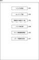
- FIG. 16 is a block diagram illustrating another configuration example of a main processing unit that performs processing related to the manufacture of the gate portion of the transfer transistor 120 included in the vertical transistor manufacturing unit 231.
- the vertical transistor manufacturing unit 231 includes a mask forming unit 241, an etching unit 242, a conductive impurity implantation unit 243, a non-conductive impurity implantation unit 251, a mask removal unit 244, and a gate insulation.
- a film deposition portion 245 and a gate electrode formation portion 247 are included.
- the non-conductive type impurity implantation unit 251 performs a process related to the implantation of non-conductive type impurities.
- the film thickness of the oxide film that is, the gate insulating film 122
- the non-conductive impurity implantation portion 251 can control the thickness of the gate insulating film 122 by controlling the injection amount (concentration) of the non-conductive impurity implanted into the trench.
- the non-conductive impurity implantation portion 251 controls the film thickness of the gate insulating film 122 (that is, the charge transfer channel) by controlling the implantation amount (concentration) of the non-conductive impurity in accordance with the depth direction of the groove. (Potential depth) can be controlled in the depth direction of the groove (that is, in the charge transfer direction).
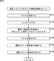
- the vertical transistor manufacturing unit 231 can manufacture, for example, the gate portions of the examples described with reference to FIGS. That is, the image sensor manufacturing unit 202 can manufacture the image sensor 100 including the transfer transistor 120 as in each example described with reference to FIGS.
- the mask formation part 241 to the conductive impurity implantation part 243 perform the processes in steps S141 to S143 and the processes in steps S101 to S103 in FIG. Run in the same way as
- step S144 the non-conductive impurity implantation portion 251 implants a non-conductive impurity at a concentration corresponding to the depth of the bottom surface or side surface of the groove formed in step S142.
- step S145 the mask removing unit 244 removes the mask as in the case of FIG.
- step S146 the gate insulating film depositing portion 245 deposits the gate insulating film 122 with a predetermined film thickness in the trench formed in step S142.
- the gate insulating film 122 has a thickness corresponding to the concentration of the non-conductive impurities by accelerated oxidation. That is, the gate insulating film 122 has a thickness corresponding to the depth of the groove.
- step S147 the gate electrode formation portion 247 forms the gate electrode 123 in the groove portion of the gate insulating film 122 formed as described above.
- step S147 the vertical transistor gate manufacturing process is completed.
- the vertical transistor manufacturing unit 231 can manufacture, for example, the gate portion of the transfer transistor 120 in each example described with reference to FIGS.
- the non-conductive impurity implantation part 251 is formed by the process of step S146 by injecting the non-conductive impurity while changing its concentration stepwise in the depth direction of the groove. Since the film thickness of the gate insulating film 122 changes stepwise in the depth direction, the vertical transistor manufacturing unit 231 has, for example, the transfer transistor 120 of each example described with reference to FIGS. A gate part can be manufactured.
- the non-conductive impurity implantation part 251 is formed by the process of step S146 by injecting non-conductive impurities by gradually changing the concentration thereof in the depth direction of the groove. Since the thickness of the gate insulating film 122 gradually changes in the depth direction, the vertical transistor manufacturing unit 231 includes, for example, the gate portion of the transfer transistor 120 in each example described with reference to FIGS. 4 and 6. Can be manufactured.
- the image sensor manufacturing unit 202 can manufacture the image sensor 100 including the transfer transistor 120 as in the example described with reference to FIGS.
- FIG. 18 is a block diagram showing still another configuration example of a main processing unit that performs processing related to manufacturing of the gate portion of the transfer transistor 120 included in the vertical transistor manufacturing unit 231.
- the vertical transistor manufacturing unit 231 includes a mask forming unit 241, an etching unit 242, a conductive impurity implantation unit 243, a mask removing unit 244, a gate insulating film deposition unit 245, and a gate.
- An electrode formation portion 247 is included.
- the conductivity type impurity implantation part 243 implants the conductivity type impurity at a concentration according to the depth of the position where the groove is implanted.
- the conductive impurity implanted portion 243 allows the potential depth of the charge transfer channel 121 to be in the depth direction of the groove (that is, in the charge transfer direction). ) Can be controlled. That is, the conductivity type impurity implantation part 243 can form a potential gradient in the charge transfer direction in the charge transfer channel 121.
- the vertical transistor manufacturing unit 231 has the concentration of the conductive impurity injected into the charge transfer channel 121 as in the example described with reference to FIG. A gate portion that changes in the transfer direction can be manufactured. That is, the image sensor manufacturing unit 202 includes the transfer transistor 120 in which the concentration of the conductive impurity injected into the charge transfer channel 121 changes in the charge transfer direction, such as the example described with reference to FIG. 100 can be manufactured.
- the mask forming unit 241 and the etching unit 242 perform the processes in steps S161 and S162 in the same manner as the processes in steps S101 and S102 in FIG. Execute.
- step S163 the conductivity type impurity implantation part 243 implants the conductivity type impurity into the groove formed in step S162 at a concentration according to the depth of the position where the impurity is implanted.
- step S164 the mask removing unit 244 removes the mask as in the case of FIG.
- step S165 the gate insulating film deposited portion 245 deposits the gate insulating film 122 with a predetermined film thickness on the groove formed in step S162.
- step S166 the gate electrode forming portion 247 forms the gate electrode 123 in the groove portion of the gate insulating film 122 formed as described above.
- step S166 When the process in step S166 is completed, the vertical transistor gate manufacturing process is completed.
- the vertical transistor manufacturing unit 231 has the concentration of the conductive impurity injected into the charge transfer channel 121 as in the example described with reference to FIG.
- the gate portion of the transfer transistor 120 that changes to can be manufactured. That is, the image sensor manufacturing unit 202 includes the transfer transistor 120 in which the concentration of the conductive impurity injected into the charge transfer channel 121 changes in the charge transfer direction, such as the example described with reference to FIG. 100 can be manufactured.
- the vertical transistor manufacturing unit 231 may have the same configuration as the example described with reference to FIG. That is, the vertical transistor manufacturing unit 231 may include the mask formation unit 241 to the gate electrode formation unit 247.
- the mask forming part 241 to the gate insulating film deposition part 245 perform the processes in steps S201 to S205 and the processes in steps S121 to S125 in FIG. Execute in the same way as the processing.
- step S206 the gate insulating film processing unit 246 processes the gate insulating film 122 deposited in step S205 so that the gate insulating film 122 has a thickness corresponding to the position in the rotation direction.
- a groove is formed in 122.
- the gate insulating film processing portion 246 forms the groove portion in the gate insulating film 122 as in the example of FIG. 11A or FIG. It can be changed accordingly.
- step S207 the gate electrode formation portion 247 forms the gate electrode 123 in the groove portion of the gate insulating film 122 formed in step S206.
- step S207 When the process in step S207 is completed, the vertical transistor gate manufacturing process is completed.
- the vertical transistor manufacturing unit 231 causes the film thickness of the gate insulating film 122 to gradually or stepwise in the rotation direction as in the example described with reference to FIGS.
- a gate portion of the transfer transistor 120 that changes in a shape can be manufactured. That is, the image sensor manufacturing unit 202 can manufacture the image sensor 100 including the transfer transistor 120 as in the example described with reference to FIGS. 10 and 11.
- the vertical transistor manufacturing unit 231 may have the same configuration as the example described with reference to FIG. That is, the vertical transistor manufacturing unit 231 may include the mask formation unit 241 to the gate insulating film deposition unit 245 and the gate electrode formation unit 247.
- the mask forming unit 241 and the etching unit 242 perform the processes in steps S221 and S222 in the same manner as the processes in steps S161 and S162 in FIG. Execute.
- step S223 the conductivity type impurity implantation unit 243 implants the conductivity type impurity into the groove formed in step S222 at a concentration according to the position in the rotational direction of the implantation.
- the mask removal unit 244, the gate insulating film deposition unit 245, and the gate electrode formation unit 247 execute the processes in steps S224 to S226 in the same manner as the processes in steps S164 to S166 in FIG.
- step S226 When the processing in step S226 is completed, the vertical transistor gate manufacturing process is completed.
- the vertical transistor manufacturing unit 231 can remove the conductive impurities injected into the charge transfer channel 121 such as the example described with reference to FIG.
- the gate portion of the transfer transistor 120 whose concentration changes in the rotation direction can be manufactured. That is, the image sensor manufacturing unit 202 transfers the transfer transistor 120 in which the concentration of the conductive impurity injected into the charge transfer channel 121 changes in the rotation direction, such as the example described with reference to FIGS. 10 and 11C. Can be manufactured.
- the image sensor 100 (image pickup device) manufactured by applying the present technology described above can be applied to a device such as an image pickup apparatus, for example. That is, the present technology can be implemented not only as an image sensor, but also as a device (for example, an image pickup apparatus) using the image sensor.
- FIG. 22 is a block diagram illustrating a main configuration example of an imaging apparatus as an example of an electronic apparatus to which the present technology is applied.
- An imaging apparatus 600 shown in FIG. 22 is an apparatus that images a subject and outputs an image of the subject as an electrical signal.
- the imaging apparatus 600 includes an optical unit 611, a CMOS sensor 612, an A / D converter 613, an operation unit 614, a control unit 615, an image processing unit 616, a display unit 617, a codec processing unit 618, and A recording unit 619 is included.
- the optical unit 611 includes a lens that adjusts the focal point to the subject and collects light from the focused position, an aperture that adjusts exposure, a shutter that controls the timing of imaging, and the like.
- the optical unit 611 transmits light (incident light) from the subject and supplies the light to the CMOS sensor 612.
- the CMOS sensor 612 photoelectrically converts incident light and supplies a signal (pixel signal) for each pixel to the A / D converter 613.
- the A / D converter 613 converts the pixel signal supplied from the CMOS sensor 612 at a predetermined timing into digital data (image data), and sequentially supplies it to the image processing unit 616 at the predetermined timing.
- the operation unit 614 includes, for example, an arbitrary input device such as a jog dial (trademark), a key, a button, or a touch panel.
- the operation unit 614 receives an operation input by a user and supplies a signal corresponding to the operation input to the control unit 615. .
- the control unit 615 is based on a signal corresponding to the user's operation input input by the operation unit 614, the optical unit 611, the CMOS sensor 612, the A / D converter 613, the image processing unit 616, the display unit 617, and codec processing.
- the driving of the unit 618 and the recording unit 619 is controlled to cause each unit to perform processing related to imaging.
- the image processing unit 616 performs, for example, color mixture correction, black level correction, white balance adjustment, demosaic processing, matrix processing, gamma correction, and YC conversion on the image data supplied from the A / D converter 613. Various image processing is performed.
- the image processing unit 616 supplies the image data subjected to the image processing to the display unit 617 and the codec processing unit 618.
- the display unit 617 is configured as a liquid crystal display, for example, and displays an image of the subject based on the image data supplied from the image processing unit 616.
- the codec processing unit 618 performs a predetermined encoding process on the image data supplied from the image processing unit 616, and supplies the obtained encoded data to the recording unit 619.
- the recording unit 619 records the encoded data from the codec processing unit 618.
- the encoded data recorded in the recording unit 619 is read out and decoded by the image processing unit 616 as necessary.
- the image data obtained by the decoding process is supplied to the display unit 617, and a corresponding image is displayed.
- the present technology described above is applied to the CMOS sensor 612 of the imaging apparatus 600 as described above. That is, the image sensor 100 to which the present technology is applied is used for the CMOS sensor 612. Therefore, the CMOS sensor 612 includes a vertical transistor having a potential gradient in at least a part of the charge transfer channel that transfers the charge of the photoelectric conversion unit. Therefore, the CMOS sensor 612 can make it easier to transfer charges. Therefore, the imaging apparatus 600 can obtain a higher quality image by imaging the subject (a reduction in the quality of the captured image can be suppressed).
- the imaging apparatus to which the present technology is applied is not limited to the configuration described above, and may have another configuration.
- an information processing apparatus having an imaging function such as a mobile phone, a smart phone, a tablet device, and a personal computer.
- it may be a camera module used by being mounted on another information processing apparatus (or mounted as an embedded device).
- this recording medium includes a removable medium 221 on which a program is recorded, which is distributed to distribute the program to the user, separately from the apparatus main body.
- the removable medium 221 includes a magnetic disk (including a flexible disk) and an optical disk (including a CD-ROM and a DVD). Further, magneto-optical disks (including MD (Mini-Disc)) and semiconductor memories are also included.
- MD Mini-Disc
- This program can also be provided via a wired or wireless transmission medium such as a local area network, the Internet, or digital satellite broadcasting.
- the program can be received by the communication unit 214 and installed in the storage unit 213.
- this program can also be installed in advance in a storage unit or ROM.
- the program can be installed in advance in a ROM or the like built in the storage unit 213 or the control unit 201.
- the program executed by the computer may be a program that is processed in time series in the order described in this specification, or in parallel or at a necessary timing such as when a call is made. It may be a program for processing.
- the step of describing the program recorded on the recording medium is not limited to the processing performed in chronological order according to the described order, but may be performed in parallel or It also includes processes that are executed individually.
- each step described above can be executed in each device described above or any device other than each device described above.
- the device that executes the process may have the functions (functional blocks and the like) necessary for executing the process described above.
- Information necessary for processing may be transmitted to the apparatus as appropriate.
- the system means a set of a plurality of components (devices, modules (parts), etc.), and it does not matter whether all the components are in the same housing. Accordingly, a plurality of devices housed in separate housings and connected via a network and a single device housing a plurality of modules in one housing are all systems. .
- the configuration described as one device (or processing unit) may be divided and configured as a plurality of devices (or processing units).
- the configurations described above as a plurality of devices (or processing units) may be combined into a single device (or processing unit).
- a configuration other than that described above may be added to the configuration of each device (or each processing unit).
- a part of the configuration of a certain device (or processing unit) may be included in the configuration of another device (or other processing unit). .
- the present technology can take a configuration of cloud computing in which one function is shared by a plurality of devices via a network and is jointly processed.
- each step described in the above flowchart can be executed by one device or can be shared by a plurality of devices.
- the plurality of processes included in the one step can be executed by being shared by a plurality of apparatuses in addition to being executed by one apparatus.
- the present technology is not limited to this, and any configuration mounted on such a device or a device constituting the system, for example, a processor as a system LSI (Large Scale Integration), a module using a plurality of processors, a plurality of It is also possible to implement as a unit using other modules, a set obtained by further adding other functions to the unit (that is, a partial configuration of the apparatus), and the like.
- a processor as a system LSI (Large Scale Integration)
- a module using a plurality of processors a plurality of It is also possible to implement as a unit using other modules, a set obtained by further adding other functions to the unit (that is, a partial configuration of the apparatus), and the like.
- this technique can also take the following structures.
- An imaging device including a vertical transistor having a potential gradient in at least a part of a charge transfer channel that transfers charges of a photoelectric conversion unit.
- the imaging device according to (1) wherein the potential has a gradient that becomes deeper toward a transfer destination of the charge in a charge transfer direction in the charge transfer channel.
- the charge transfer channel is a first conductivity type charge transfer channel that transfers charges of the photoelectric conversion unit of the second conductivity type formed in the first conductivity type semiconductor,
- the imaging element according to (2) wherein a gate insulating film formed between the charge transfer channel and the gate electrode is formed so that the film thickness gradually decreases toward the charge transfer destination.
- the charge transfer channel is a first conductivity type charge transfer channel that transfers charges of the photoelectric conversion unit of the second conductivity type formed in the first conductivity type semiconductor,
- the imaging element according to (2) wherein a gate insulating film formed between the charge transfer channel and the gate electrode is formed so that the film thickness decreases stepwise toward the charge transfer destination.
- the charge transfer channel is a first conductivity type charge transfer channel that transfers charges of the photoelectric conversion unit of the second conductivity type formed in the first conductivity type semiconductor, The imaging device according to any one of (2) to (4), wherein the charge transfer channel is formed so that an impurity concentration decreases toward a transfer destination of the charge.
- the charge transfer channel is a second conductivity type charge transfer channel that transfers charges of the photoelectric conversion unit of the second conductivity type formed in the first conductivity type semiconductor, The imaging element according to (2), wherein a gate insulating film formed between the charge transfer channel and the gate electrode is formed so that the film thickness gradually increases toward the charge transfer destination.
- the charge transfer channel is a second conductivity type charge transfer channel that transfers a charge of the photoelectric conversion unit of the second conductivity type formed in the first conductivity type semiconductor, The imaging element according to (2), wherein a gate insulating film formed between the charge transfer channel and the gate electrode is formed so that a film thickness increases stepwise toward the charge transfer destination.
- the charge transfer channel is a second conductivity type charge transfer channel that transfers charges of the photoelectric conversion unit of the second conductivity type formed in the first conductivity type semiconductor,
- An imaging device including a vertical transistor having a potential gradient in at least a part of a charge transfer channel that transfers a charge of the photoelectric conversion unit;
- An image processing apparatus comprising: an image processing unit that performs image processing on captured image data obtained by the image sensor.
- a manufacturing apparatus for manufacturing an image sensor A manufacturing apparatus comprising: a vertical transistor manufacturing unit that manufactures a vertical transistor having a potential gradient in at least a part of a charge transfer channel that transfers charges of a photoelectric conversion unit.
- the vertical transistor manufacturing department An etching portion for etching the semiconductor substrate to form a groove; A conductive impurity implantation portion for implanting a conductive impurity into the groove formed by the etching portion; A gate insulating film forming portion for forming a gate insulating film in a film thickness according to a hierarchy in the groove portion; A gate insulating film removing unit that removes the gate insulating film formed by the gate insulating film forming unit to a depth corresponding to the hierarchy; A gate electrode forming portion for forming a gate electrode in a groove formed in the gate insulating film, By repeating the formation of the gate insulating film by the gate insulating film forming portion and the removal of the gate insulating film by the gate insulating film removing portion, the thickness of the gate insulating film is increased toward the charge transfer destination.
- the vertical transistor manufacturing department An etching portion for etching the semiconductor substrate to form a groove; A conductive impurity implantation portion for implanting a conductive impurity into the groove formed by the etching portion; A gate insulating film forming portion for forming a gate insulating film in the groove; A gate insulating film processing portion for forming a mesa-shaped groove in the gate insulating film formed by the gate insulating film forming portion;
- the vertical transistor manufacturing department An etching portion for etching the semiconductor substrate to form a groove; A conductive impurity implantation portion for implanting a conductive impurity into the groove formed by the etching portion; A non-conductive impurity implanted portion for injecting a non-conductive impurity into the groove formed by the etched portion at a concentration according to the depth; A gate insulating film forming portion for forming a gate insulating film in the groove;
- the vertical transistor manufacturing department An etching portion for etching the semiconductor substrate to form a groove; A conductivity type impurity implantation part for implanting a conductivity type impurity in the groove formed by the etching part at a concentration according to the depth; A gate insulating film forming portion for forming a gate insulating film in the groove; The manufacturing apparatus according to any one of (13) to (16), further including: a gate electrode forming portion that forms a gate electrode in a groove portion formed in the gate insulating film.
- the vertical transistor manufacturing department An etching portion for etching the semiconductor substrate to form a groove; A conductive impurity implantation portion for implanting a conductive impurity into the groove formed by the etching portion; A gate insulating film forming portion for forming a gate insulating film in the groove; A gate insulating film processing unit that forms a groove in the gate insulating film formed by the gate insulating film forming unit so that a film thickness of the gate insulating film changes in a rotation direction along a gate electrode; (13) The manufacturing apparatus according to any one of (13) to (17), further including: a gate electrode forming portion that forms the gate electrode in the groove portion formed by the gate insulating film processing portion.
- the vertical transistor manufacturing department An etching portion for etching the semiconductor substrate to form a groove; A conductive impurity implantation part for injecting a conductive impurity into the groove formed by the etching part at a concentration according to the position in the rotational direction along the gate electrode; A gate insulating film forming portion for forming a gate insulating film in the groove; The manufacturing apparatus according to any one of (13) to (18), further comprising: a gate electrode forming portion that forms a gate electrode in a groove portion formed in the gate insulating film. (20) A manufacturing method of a manufacturing apparatus for manufacturing an imaging device, A manufacturing method for manufacturing a vertical transistor having a potential gradient in at least a part of a charge transfer channel for transferring a charge of a photoelectric conversion unit.
- 100 image sensor 110 semiconductor substrate layer, 111 semiconductor substrate, 112 photoelectric conversion unit, 114 floating diffusion layer, 115 insulating film, 120 transfer transistor, 121 charge transfer channel, 122 gate insulating film, 123 gate electrode, 124 floating diffusion layer, 130 wiring layer, 131 wiring interlayer film, 132 and 133 wiring, 141 insulating film, 142 organic photoelectric conversion film, 143 lower transparent electrode, 144 upper transparent electrode, 145 through electrode, 146 contact, 151 passivation layer, 152 on-chip lens, 171 charge transfer channel, 200 manufacturing device, 201 control unit, 202 image sensor manufacturing unit, 211 input unit, 212 output unit, 213 storage , 214 communication unit, 215 drive, 221 removable media, 231 vertical transistor manufacturing unit, 241 mask formation unit, 242 etching unit, 243 conductivity type impurity implantation unit, 244 mask removal unit, 245 gate insulating film deposition unit, 246 gate Insulating film processing part, 247 gate electrode forming part, 251 non-conductive type im
Landscapes
- Solid State Image Pick-Up Elements (AREA)
- Transforming Light Signals Into Electric Signals (AREA)
- Metal-Oxide And Bipolar Metal-Oxide Semiconductor Integrated Circuits (AREA)
- Insulated Gate Type Field-Effect Transistor (AREA)
Abstract
La présente technologie se rapporte à un élément de capture d'image, à un dispositif de capture d'image et un dispositif et à un procédé de fabrication qui facilitent le transfert de charge. Un élément de capture d'image selon la présente technologie est pourvu d'un transistor vertical ayant un gradient de potentiel dans au moins une partie d'un canal de transfert de charge pour transférer la charge dans une unité de conversion photoélectrique. Un dispositif de capture d'image selon la présente technologie est pourvu d'un élément de capture d'image pourvu d'un transistor vertical ayant un gradient de potentiel dans au moins une partie d'un canal de transfert de charge pour transférer la charge dans une unité de conversion photoélectrique, et d'une unité de traitement d'image qui effectue un traitement d'image sur des données d'image capturée obtenues par l'élément de capture d'image. En outre, un dispositif de fabrication selon la présente technologie est pourvu d'une unité de fabrication de transistor vertical pour fabriquer un transistor vertical ayant un gradient de potentiel dans au moins une partie d'un canal de transfert de charge pour transférer la charge dans une unité de conversion photoélectrique. La présente technologie peut être appliquée, par exemple, à un élément de capture d'image, un dispositif de capture d'image et des dispositif et procédés de fabrication.
Priority Applications (4)
| Application Number | Priority Date | Filing Date | Title |
|---|---|---|---|
| CN201680011140.6A CN107251228B (zh) | 2015-02-27 | 2016-02-12 | 图像捕获元件、图像捕获装置以及制造设备和方法 |
| US15/549,315 US10825850B2 (en) | 2015-02-27 | 2016-02-12 | Imaging element, imaging device, and manufacturing apparatus and method |
| US17/027,486 US11211413B2 (en) | 2015-02-27 | 2020-09-21 | Imaging element, imaging device, and manufacturing apparatus and method |
| US17/538,230 US11961857B2 (en) | 2015-02-27 | 2021-11-30 | Imaging element, imaging device, and manufacturing apparatus and method |
Applications Claiming Priority (2)
| Application Number | Priority Date | Filing Date | Title |
|---|---|---|---|
| JP2015-037564 | 2015-02-27 | ||
| JP2015037564A JP2016162788A (ja) | 2015-02-27 | 2015-02-27 | 撮像素子、撮像装置、並びに、製造装置および方法 |
Related Child Applications (2)
| Application Number | Title | Priority Date | Filing Date |
|---|---|---|---|
| US15/549,315 A-371-Of-International US10825850B2 (en) | 2015-02-27 | 2016-02-12 | Imaging element, imaging device, and manufacturing apparatus and method |
| US17/027,486 Continuation US11211413B2 (en) | 2015-02-27 | 2020-09-21 | Imaging element, imaging device, and manufacturing apparatus and method |
Publications (1)
| Publication Number | Publication Date |
|---|---|
| WO2016136487A1 true WO2016136487A1 (fr) | 2016-09-01 |
Family
ID=56788440
Family Applications (1)
| Application Number | Title | Priority Date | Filing Date |
|---|---|---|---|
| PCT/JP2016/054068 Ceased WO2016136487A1 (fr) | 2015-02-27 | 2016-02-12 | Élément de capture d'image, dispositif de capture d'image et dispositif et procédé de fabrication |
Country Status (4)
| Country | Link |
|---|---|
| US (3) | US10825850B2 (fr) |
| JP (1) | JP2016162788A (fr) |
| CN (1) | CN107251228B (fr) |
| WO (1) | WO2016136487A1 (fr) |
Cited By (5)
| Publication number | Priority date | Publication date | Assignee | Title |
|---|---|---|---|---|
| WO2021015011A1 (fr) * | 2019-07-19 | 2021-01-28 | ソニーセミコンダクタソリューションズ株式会社 | Dispositif de capture d'image |
| WO2022124131A1 (fr) * | 2020-12-11 | 2022-06-16 | ソニーセミコンダクタソリューションズ株式会社 | Élément de réception de lumière, dispositif de réception de lumière et appareil électronique |
| WO2022259855A1 (fr) * | 2021-06-11 | 2022-12-15 | ソニーセミコンダクタソリューションズ株式会社 | Dispositif à semi-conducteur, son procédé de fabrication et appareil électronique |
| WO2023199642A1 (fr) * | 2022-04-15 | 2023-10-19 | ソニーセミコンダクタソリューションズ株式会社 | Dispositif de détection de lumière et appareil électronique |
| WO2024096095A1 (fr) * | 2022-11-02 | 2024-05-10 | ソニーセミコンダクタソリューションズ株式会社 | Élément d'imagerie et dispositif électronique |
Families Citing this family (11)
| Publication number | Priority date | Publication date | Assignee | Title |
|---|---|---|---|---|
| JP2016162788A (ja) | 2015-02-27 | 2016-09-05 | ソニー株式会社 | 撮像素子、撮像装置、並びに、製造装置および方法 |
| JP2018190797A (ja) * | 2017-04-28 | 2018-11-29 | ソニーセミコンダクタソリューションズ株式会社 | 固体撮像素子および電子機器 |
| US11843020B2 (en) * | 2017-10-30 | 2023-12-12 | Samsung Electronics Co., Ltd. | Image sensor |
| KR102542614B1 (ko) * | 2017-10-30 | 2023-06-15 | 삼성전자주식회사 | 이미지 센서 |
| JP2021019171A (ja) * | 2019-07-24 | 2021-02-15 | ソニーセミコンダクタソリューションズ株式会社 | 固体撮像素子および電子機器 |
| US11302727B2 (en) * | 2019-11-20 | 2022-04-12 | Omnivision Technologies, Inc. | Pixel, associated image sensor, and method |
| CN114631187B (zh) * | 2019-12-16 | 2026-03-24 | 索尼半导体解决方案公司 | 固态成像装置和电子设备 |
| CN111146224A (zh) * | 2019-12-23 | 2020-05-12 | 上海华力微电子有限公司 | 图像传感器及电荷转移方法 |
| CN116670815A (zh) * | 2020-12-21 | 2023-08-29 | 索尼半导体解决方案公司 | 成像设备和电子设备 |
| KR20250136348A (ko) * | 2023-01-17 | 2025-09-16 | 소니 세미컨덕터 솔루션즈 가부시키가이샤 | 반도체 장치 |
| WO2025121221A1 (fr) * | 2023-12-08 | 2025-06-12 | ソニーセミコンダクタソリューションズ株式会社 | Dispositif de détection de lumière |
Citations (5)
| Publication number | Priority date | Publication date | Assignee | Title |
|---|---|---|---|---|
| JPH0258340A (ja) * | 1988-07-07 | 1990-02-27 | Tektronix Inc | 電荷結合装置のセル |
| JP2009088186A (ja) * | 2007-09-28 | 2009-04-23 | Sanyo Electric Co Ltd | トレンチゲート型トランジスタ及びその製造方法 |
| JP2011096829A (ja) * | 2009-10-29 | 2011-05-12 | Elpida Memory Inc | 半導体装置の製造方法 |
| JP2012049499A (ja) * | 2010-07-27 | 2012-03-08 | Denso Corp | 半導体装置およびその制御方法 |
| JP2015012241A (ja) * | 2013-07-01 | 2015-01-19 | ソニー株式会社 | 撮像素子およびその製造方法、ならびに電子機器 |
Family Cites Families (15)
| Publication number | Priority date | Publication date | Assignee | Title |
|---|---|---|---|---|
| US5065203A (en) | 1988-07-07 | 1991-11-12 | Tektronix, Inc. | Trench structured charge-coupled device |
| JPH02181863A (ja) | 1989-01-06 | 1990-07-16 | Matsushita Electric Ind Co Ltd | 学習機械 |
| US7382019B2 (en) * | 2005-04-26 | 2008-06-03 | Fairchild Semiconductor Corporation | Trench gate FETs with reduced gate to drain charge |
| US8076720B2 (en) | 2007-09-28 | 2011-12-13 | Semiconductor Components Industries, Llc | Trench gate type transistor |
| EP2133918B1 (fr) * | 2008-06-09 | 2015-01-28 | Sony Corporation | Dispositif d'imagerie à l'état solide, son procédé de commande, et appareil électronique |
| JP5407282B2 (ja) | 2008-11-07 | 2014-02-05 | ソニー株式会社 | 固体撮像装置とその製造方法、及び電子機器 |
| JP2010287743A (ja) * | 2009-06-11 | 2010-12-24 | Sony Corp | 半導体装置及びその製造方法、固体撮像素子 |
| DE102011079747A1 (de) | 2010-07-27 | 2012-02-02 | Denso Corporation | Halbleitervorrichtung mit Schaltelement und Freilaufdiode, sowie Steuerverfahren hierfür |
| CN104157685B (zh) | 2010-07-27 | 2018-01-16 | 株式会社电装 | 具有开关元件和续流二极管的半导体装置及其控制方法 |
| US9570489B2 (en) * | 2011-07-12 | 2017-02-14 | Sony Corporation | Solid state imaging device having impurity concentration on light receiving surface being greater or equal to that on opposing surface |
| CN103782390B (zh) * | 2011-08-11 | 2016-11-16 | 沃特拉半导体公司 | 垂直栅极射频横向扩散金氧半场效晶体管(ldmos)装置 |
| US9634134B2 (en) * | 2011-10-13 | 2017-04-25 | Taiwan Semiconductor Manufacturing Company, Ltd. | Embedded transistor |
| JP6131689B2 (ja) * | 2013-04-16 | 2017-05-24 | 住友電気工業株式会社 | 炭化珪素半導体装置の製造方法 |
| US9306058B2 (en) * | 2013-10-02 | 2016-04-05 | Infineon Technologies Ag | Integrated circuit and method of manufacturing an integrated circuit |
| JP2016162788A (ja) * | 2015-02-27 | 2016-09-05 | ソニー株式会社 | 撮像素子、撮像装置、並びに、製造装置および方法 |
-
2015
- 2015-02-27 JP JP2015037564A patent/JP2016162788A/ja active Pending
-
2016
- 2016-02-12 US US15/549,315 patent/US10825850B2/en active Active
- 2016-02-12 CN CN201680011140.6A patent/CN107251228B/zh active Active
- 2016-02-12 WO PCT/JP2016/054068 patent/WO2016136487A1/fr not_active Ceased
-
2020
- 2020-09-21 US US17/027,486 patent/US11211413B2/en not_active Expired - Fee Related
-
2021
- 2021-11-30 US US17/538,230 patent/US11961857B2/en active Active
Patent Citations (5)
| Publication number | Priority date | Publication date | Assignee | Title |
|---|---|---|---|---|
| JPH0258340A (ja) * | 1988-07-07 | 1990-02-27 | Tektronix Inc | 電荷結合装置のセル |
| JP2009088186A (ja) * | 2007-09-28 | 2009-04-23 | Sanyo Electric Co Ltd | トレンチゲート型トランジスタ及びその製造方法 |
| JP2011096829A (ja) * | 2009-10-29 | 2011-05-12 | Elpida Memory Inc | 半導体装置の製造方法 |
| JP2012049499A (ja) * | 2010-07-27 | 2012-03-08 | Denso Corp | 半導体装置およびその制御方法 |
| JP2015012241A (ja) * | 2013-07-01 | 2015-01-19 | ソニー株式会社 | 撮像素子およびその製造方法、ならびに電子機器 |
Cited By (9)
| Publication number | Priority date | Publication date | Assignee | Title |
|---|---|---|---|---|
| WO2021015011A1 (fr) * | 2019-07-19 | 2021-01-28 | ソニーセミコンダクタソリューションズ株式会社 | Dispositif de capture d'image |
| JPWO2021015011A1 (fr) * | 2019-07-19 | 2021-01-28 | ||
| JP7615028B2 (ja) | 2019-07-19 | 2025-01-16 | ソニーセミコンダクタソリューションズ株式会社 | 撮像装置 |
| WO2022124131A1 (fr) * | 2020-12-11 | 2022-06-16 | ソニーセミコンダクタソリューションズ株式会社 | Élément de réception de lumière, dispositif de réception de lumière et appareil électronique |
| JPWO2022124131A1 (fr) * | 2020-12-11 | 2022-06-16 | ||
| JP7826226B2 (ja) | 2020-12-11 | 2026-03-09 | ソニーセミコンダクタソリューションズ株式会社 | 受光素子、受光装置及び電子機器 |
| WO2022259855A1 (fr) * | 2021-06-11 | 2022-12-15 | ソニーセミコンダクタソリューションズ株式会社 | Dispositif à semi-conducteur, son procédé de fabrication et appareil électronique |
| WO2023199642A1 (fr) * | 2022-04-15 | 2023-10-19 | ソニーセミコンダクタソリューションズ株式会社 | Dispositif de détection de lumière et appareil électronique |
| WO2024096095A1 (fr) * | 2022-11-02 | 2024-05-10 | ソニーセミコンダクタソリューションズ株式会社 | Élément d'imagerie et dispositif électronique |
Also Published As
| Publication number | Publication date |
|---|---|
| US20180033816A1 (en) | 2018-02-01 |
| JP2016162788A (ja) | 2016-09-05 |
| CN107251228B (zh) | 2021-03-16 |
| US11961857B2 (en) | 2024-04-16 |
| US20210005654A1 (en) | 2021-01-07 |
| US20220093663A1 (en) | 2022-03-24 |
| US11211413B2 (en) | 2021-12-28 |
| CN107251228A (zh) | 2017-10-13 |
| US10825850B2 (en) | 2020-11-03 |
Similar Documents
| Publication | Publication Date | Title |
|---|---|---|
| US11961857B2 (en) | Imaging element, imaging device, and manufacturing apparatus and method | |
| CN103022065B (zh) | 成像元件、图像拾取装置、制造装置和制造方法 | |
| CN107615487B (zh) | 成像元件、电子器件、制造设备以及制造方法 | |
| TWI479648B (zh) | 固態成像裝置及其製造方法及電子設備 | |
| US7579638B2 (en) | Solid-state image pickup device and manufacturing method thereof | |
| CN105826336A (zh) | 固态摄像装置及固态摄像装置的制造方法 | |
| CN205582940U (zh) | 图像传感器 | |
| CN116802811A (zh) | 摄像元件和摄像装置 | |
| CN103579270B (zh) | 图像传感器、成像装置及制造图像传感器的装置及方法 | |
| CN109411490B (zh) | 用于减少暗电流的凸起电极 | |
| CN1819252A (zh) | 固态图像拾取装置及其制造方法 | |
| CN1523879A (zh) | 固体摄像装置及其制造方法 | |
| CN1819242A (zh) | Cmos图像传感器及其制造方法 | |
| KR101543098B1 (ko) | 고체 촬상 장치 및 고체 촬상 장치의 제조 방법 | |
| WO2022044797A1 (fr) | Dispositif à semi-conducteur, dispositif d'imagerie et appareil électronique | |
| CN102906876B (zh) | 具有经掺杂的传输栅极的图像传感器 | |
| US10128299B1 (en) | Manufacturing method of image sensor including source follower contact to floating diffusion | |
| JP2007095791A (ja) | 撮像装置の製造方法 | |
| CN1790670A (zh) | 制造cmos图像传感器的方法 | |
| CN103715213A (zh) | 固态成像装置和电子装置 | |
| CN1819244A (zh) | Cmos图像传感器及其制造方法 | |
| JP5539426B2 (ja) | 撮像装置の製造方法 | |
| JP2014127514A (ja) | 固体撮像素子、固体撮像素子の製造方法および電子機器 | |
| CN108400141A (zh) | 具有反向倒置型源极跟随器的图像传感器 | |
| CN108470743A (zh) | 图像传感器的形成方法 |
Legal Events
| Date | Code | Title | Description |
|---|---|---|---|
| 121 | Ep: the epo has been informed by wipo that ep was designated in this application |
Ref document number: 16755234 Country of ref document: EP Kind code of ref document: A1 |
|
| NENP | Non-entry into the national phase |
Ref country code: DE |
|
| 122 | Ep: pct application non-entry in european phase |
Ref document number: 16755234 Country of ref document: EP Kind code of ref document: A1 |