WO2016139934A1 - Électrode transparente, et élément organique à électroluminescence - Google Patents
Électrode transparente, et élément organique à électroluminescence Download PDFInfo
- Publication number
- WO2016139934A1 WO2016139934A1 PCT/JP2016/001103 JP2016001103W WO2016139934A1 WO 2016139934 A1 WO2016139934 A1 WO 2016139934A1 JP 2016001103 W JP2016001103 W JP 2016001103W WO 2016139934 A1 WO2016139934 A1 WO 2016139934A1
- Authority
- WO
- WIPO (PCT)
- Prior art keywords
- layer
- transparent electrode
- derivative
- metal layer
- transparent
- Prior art date
- Legal status (The legal status is an assumption and is not a legal conclusion. Google has not performed a legal analysis and makes no representation as to the accuracy of the status listed.)
- Ceased
Links
Images
Classifications
-
- H—ELECTRICITY
- H10—SEMICONDUCTOR DEVICES; ELECTRIC SOLID-STATE DEVICES NOT OTHERWISE PROVIDED FOR
- H10K—ORGANIC ELECTRIC SOLID-STATE DEVICES
- H10K50/00—Organic light-emitting devices
- H10K50/80—Constructional details
- H10K50/805—Electrodes
- H10K50/82—Cathodes
- H10K50/828—Transparent cathodes, e.g. comprising thin metal layers
-
- B—PERFORMING OPERATIONS; TRANSPORTING
- B32—LAYERED PRODUCTS
- B32B—LAYERED PRODUCTS, i.e. PRODUCTS BUILT-UP OF STRATA OF FLAT OR NON-FLAT, e.g. CELLULAR OR HONEYCOMB, FORM
- B32B15/00—Layered products comprising a layer of metal
- B32B15/04—Layered products comprising a layer of metal comprising metal as the main or only constituent of a layer, which is next to another layer of the same or of a different material
- B32B15/08—Layered products comprising a layer of metal comprising metal as the main or only constituent of a layer, which is next to another layer of the same or of a different material of synthetic resin
-
- H—ELECTRICITY
- H05—ELECTRIC TECHNIQUES NOT OTHERWISE PROVIDED FOR
- H05B—ELECTRIC HEATING; ELECTRIC LIGHT SOURCES NOT OTHERWISE PROVIDED FOR; CIRCUIT ARRANGEMENTS FOR ELECTRIC LIGHT SOURCES, IN GENERAL
- H05B33/00—Electroluminescent light sources
- H05B33/02—Details
-
- H—ELECTRICITY
- H05—ELECTRIC TECHNIQUES NOT OTHERWISE PROVIDED FOR
- H05B—ELECTRIC HEATING; ELECTRIC LIGHT SOURCES NOT OTHERWISE PROVIDED FOR; CIRCUIT ARRANGEMENTS FOR ELECTRIC LIGHT SOURCES, IN GENERAL
- H05B33/00—Electroluminescent light sources
- H05B33/12—Light sources with substantially two-dimensional [2D] radiating surfaces
- H05B33/26—Light sources with substantially two-dimensional [2D] radiating surfaces characterised by the composition or arrangement of the conductive material used as an electrode
- H05B33/28—Light sources with substantially two-dimensional [2D] radiating surfaces characterised by the composition or arrangement of the conductive material used as an electrode of translucent electrodes
Definitions
- the present invention relates to a transparent electrode and an organic electroluminescence element provided with the transparent electrode.
- organic EL elements organic electroluminescence elements
- the organic EL element includes an anode, a cathode, and an organic EL layer (light emitting functional layer) formed between the pair of electrodes.
- This organic EL layer has, for example, an organic light emitting layer, a hole injection layer, and the like.
- the organic EL element emits light by energy generated by recombination of holes and electrons in the organic light emitting layer in the organic EL layer.
- the transparent electrode on the light extraction side of such an organic EL element is generally formed using tin-doped indium oxide (Indium Thin Oxide: ITO), zinc-doped indium oxide (Indium Zinc Oxide: IZO), or the like.
- ITO Indium Thin Oxide
- IZO Indium Zinc Oxide
- this transparent electrode must form a thick and uniform film. For this reason, a decrease in light transmittance, an increase in price, a labor for high-temperature treatment in the formation process, and the like occur, and there is a limit to reducing the resistance on the film in particular (see, for example, Patent Document 1). .
- transparent electrode technology that does not use ITO has been disclosed.
- a conductive surface in which at least one fine wire structure portion of a uniform mesh shape, comb shape, or grid type metal and alloy is arranged is prepared, and a conductive polymer material is appropriately formed thereon, for example.
- a method of forming a transparent electrode having a low resistance by forming a transparent conductive layer using an ink dissolved or dispersed in an appropriate solvent using a coating method or a printing method has been proposed (for example, Patent Document 2 and Patent Document 2). 3).
- the organic EL element which employs the transparent electrode formed by combining the metal layer having the thin wire structure and the transparent conductive layer described above may easily see the metal thin wire depending on the size and shape of the metal layer, and may impair the appearance.
- the present invention is intended to solve such problems, and an object thereof is to provide a transparent electrode capable of solving the appearance that is hindered by a metal layer, and an organic EL device including the transparent electrode.
- a transparent electrode which is one embodiment of the present invention is composed of a transparent base material and a plurality of islands arranged at intervals on the transparent base material, and the width of each island is It has a 1 to 100 micrometer metal layer, and the transparent conductive layer formed on the said transparent base material so that the said metal layer may be covered, It is characterized by the above-mentioned.
- An organic electroluminescent element which is one embodiment of the present invention includes a transparent electrode which is one embodiment of the present invention.
- the appearance of the metal layer can be improved by making the metal layer into an island-like arrangement structure and further selecting the size of each island within a range that takes into consideration the human visual limit.
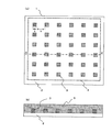
- FIG. 1A is a plan view
- FIG. 1B is a cross-sectional view taken along line A-A ′ in FIG.
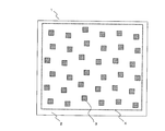
- the top view of the structure of the other transparent electrode which concerns on 1st embodiment of this invention is shown.
- the transparent electrode 1 of this embodiment is provided with the transparent base material 2, the metal layer 3, and the transparent conductive layer 5 which were arrange
- the surface resistivity of the conductive surface of the transparent electrode 1 is 0.01 ⁇ / ⁇ or more and 100 ⁇ / ⁇ or less. Preferably, it is 0.1 ⁇ / ⁇ or more and 10 ⁇ / ⁇ or less.
- the transparent electrode 1 of the present embodiment can be used for a transparent electrode 1 such as an LCD, an electroluminescence element, a plasma display, an electrochromic display, a solar battery, a touch panel, electronic paper, an electromagnetic wave shielding material, etc. It is preferable to use it for an organic EL element because of its excellent properties and high smoothness.
- the transparent base material 2 is comprised from a plastic film, a plastic plate, glass etc., for example.
- raw materials for plastic films and plastic plates include polyesters such as polyethylene terephthalate (PET) and polyethylene naphthalate, polyethylene (PE), polypropylene (PP), polystyrene, and ethylene-vinyl acetate copolymer resin (EVA).
- PET polyethylene terephthalate
- PE polyethylene
- PP polypropylene
- EVA ethylene-vinyl acetate copolymer resin
- Polyolefins polyvinyl resins such as polyvinyl chloride and polyvinylidene chloride, polyether ether ketone (PEEK), polysulfone (PSF), polyether sulfone (PES), polycarbonate (PC), polyamide, polyimide, acrylic resin, Triacetyl cellulose (TAC) or the like can be used.
- PEEK polyether ether ketone
- PSF polysulfone
- PES polyether sulfone
- PC polycarbonate
- polyamide polyimide
- acrylic resin Triacetyl cellulose (TAC) or the like
- TAC Triacetyl cellulose
- the transparent substrate 2 is preferably excellent in surface smoothness.
- the smoothness of the surface is preferably such that the arithmetic average roughness Ra is 5 nm or less and the maximum height Ry is 50 nm or less, more preferably the arithmetic average roughness Ra is 1 nm or less and Ry is 20 nm or less.
- the smoothness of the surface can be calculated from measurement using an atomic force microscope (AFM) or the like.
- the smoothness of the surface of the transparent substrate 2 may be smoothed by applying an undercoat layer such as a thermosetting resin, an ultraviolet curable resin, an electron beam curable resin, a radiation curable resin, or a machine such as polishing. It can be smoothed by processing.
- an undercoat layer such as a thermosetting resin, an ultraviolet curable resin, an electron beam curable resin, a radiation curable resin, or a machine such as polishing. It can be smoothed by processing.
- a gas barrier layer for the purpose of blocking oxygen and moisture in the atmosphere.
- metal oxide such as silicon oxide, silicon nitride, silicon oxynitride, aluminum nitride, aluminum oxide, or metal nitride can be used. These materials have an oxygen barrier function in addition to a water vapor barrier function.
- silicon nitride and silicon oxynitride having favorable barrier properties, solvent resistance, and transparency are preferable.
- the gas barrier layer can have a multi-layer structure as necessary. In that case, you may comprise only an inorganic layer and may comprise an inorganic layer and an organic layer.
- the gas barrier layer for example, a resistance heating vapor deposition method, an electron beam vapor deposition method, a reactive vapor deposition method, an ion plating method, or a sputtering method can be used depending on the material.
- the thickness of the gas barrier layer is not particularly limited, but typically it is preferably in the range of 5 nm to 500 nm per layer, more preferably 10 nm to 200 nm per layer.
- the gas barrier layer is provided on at least one surface of the transparent substrate 2 and is preferably provided on both surfaces.
- the metal layer 3 preferably has a low electric resistance, and a material having a conductivity of, for example, 10 7 S / cm or more is used.
- a material having a conductivity of, for example, 10 7 S / cm or more is used.
- a conductive material include metals such as aluminum, silver, chromium, gold, copper, tantalum, and molybdenum and / or alloys thereof.
- aluminum, chromium, copper, silver, and alloys thereof are preferable from the viewpoint of high conductivity and ease of material handling.
- the conductivity of the metal layer 3 may be equal to or higher than the conductivity of the transparent conductive layer 5 described later.
- the metal layer 3 of the present embodiment is configured by disposing the above-described conductive material at predetermined intervals in an island shape with respect to the surface of the transparent substrate 2.
- the arrangement condition is determined in consideration of the human visual limit. That is, from the relationship between spatial frequency and visual characteristics, when the viewing distance is 30 cm, the human eye cannot basically distinguish resolutions of 300 (84.7 ⁇ m) to 400 (63.5 ⁇ m) dpi or more. . For this reason, it is preferable that the size a of the island constituting the metal layer 3 is 100 ⁇ m or less as a condition that the metal layer 3 is not visually recognized.
- a size (size a) slightly larger than the visual limit range is selected.
- the plane figure of each island of the metal layer 3 is a polygon or a circle, any figure may be selected. However, it is preferable to select only one plane figure. This is because if two or more types of shapes exist adjacent to each other, the metal layer 3 may be easily visible.
- the plane figure of each island is preferably a symmetric figure shape with small anisotropy such as a regular polygon.
- the size a of the island is, for example, the length of the long side when the planar figure (planar shape) is a rectangular shape.
- the planar figure of the island is a polygonal shape, the longest length passing through the center of gravity is defined as the size a.
- the diameter is defined as a.
- the length in the direction perpendicular to the island arrangement direction on the side where the distance b between the islands is short may be defined as the island size a.
- the distance b between the islands that become the transmission region may be visually recognized.
- the visual distance since the visual distance may be closer than 30 cm, the interval slightly smaller than the visual limit is selected.
- the lower limit value of the island size a of the metal layer 3 is preferably 1 ⁇ m in consideration of technical accuracy in the process described later.
- each island of the metal layer 3 is set to 1 ⁇ m to 100 ⁇ m, and the arrangement interval b between the islands is selected within a range of 50 ⁇ m or more.
- interval b of islands is limited from the performance requested
- the height (thickness) of the metal layer 3 may be determined according to the desired conductivity, but is preferably 0.01 ⁇ m or more and 10 ⁇ m or less, and more preferably 0.1 ⁇ m or more and 1 ⁇ m or less.
- the metal layer 3 can also be made into a multilayer structure as needed. In that case, you may comprise only with the same electrically-conductive material, and you may comprise with a different electrically-conductive material.
- the light transmittance is reduced by arranging the metal layer 3, it is important that the reduction is as small as possible.
- the distance b between the islands is made too narrow or the size a of the island is set large. It is preferable that the light transmittance is 50% or more, more preferably 80% or more without being too much.
- the arrangement of the metal layer 3 may be freely arranged as long as the above conditions are included. However, as shown in FIG. 1, when arranged in an orderly manner, the metal layer 3 may be visually recognized in a linear shape depending on the size (size a) of islands, the arrangement interval b, and the viewing distance. For this reason, as shown in FIG. 2, a layout in which the metal layer 3 is more difficult to visually recognize may be selected by randomly arranging the metal layers 3.
- the transparent conductive layer 5 is formed by a coating method.
- the solution for forming the transparent conductive layer 5 includes a material that becomes the transparent conductive layer 5 and a solvent.
- the material of the transparent conductive layer 5 preferably contains a polymer compound exhibiting conductivity.
- the polymer compound may contain a dopant.
- the conductivity of the polymer compound is 10 ⁇ 5 or more and 10 5 S / cm or less, preferably 10 ⁇ 3 or more and 10 5 S / cm or less in terms of conductivity.
- the transparent conductive layer 5 consists of a high molecular compound which shows electroconductivity substantially.
- the transparent conductive layer 5 As a material constituting the transparent conductive layer 5, for example, polyaniline and derivatives thereof, polythiophene and derivatives thereof, and the like can be used.
- a known dopant can be used as the dopant, and examples thereof include organic sulfonic acids such as polystyrene sulfonic acid and dodecylbenzene sulfonic acid, and Lewis acids such as PF 5 , AsF 5 , and SbF 5 .
- the polymer compound exhibiting conductivity may be a self-doped polymer compound in which a dopant is directly bonded to the polymer compound.
- the transparent conductive layer 5 is preferably composed of polythiophene and derivatives thereof, and is substantially preferably composed of polythiophene and derivatives thereof.
- Polythiophene and its derivatives may contain a dopant. Since polythiophene, a polythiophene derivative, or a mixture of polythiophene and a polythiophene derivative is easily dissolved or dispersed in an aqueous solvent such as water and alcohol, it is preferably used as a solute of a coating solution used in a coating method. Moreover, these have high electroconductivity and are used suitably as an electrode material.
- these have a HOMO energy of about 5.0 eV, and the difference from the HOMO energy of an organic light emitting layer used in a normal organic EL element is as low as about 1 eV. Therefore, since holes can be efficiently injected into the organic light emitting layer, it can be suitably used particularly as a material for the anode. Moreover, these have high transparency and are suitably used as an electrode on the light emission extraction side of the organic EL element.
- the transparent conductive layer 5 is preferably composed of polyaniline and a derivative thereof, and is preferably substantially composed of polyaniline and a derivative thereof.
- Polyaniline and its derivatives may contain a dopant.
- Polyaniline and its derivatives are suitably used as electrode materials because they are excellent in conductivity and stability. Further, it has high transparency and is suitably used as an electrode on the light emission extraction side of the organic EL element.
- the film thickness may be determined according to the desired conductivity, but is preferably selected so that the transparent electrode 1 can obtain high smoothness.
- the transparent conductive layer 5 is preferably equal to or greater than the film thickness of the metal layer 3 as shown in FIG.
- the transparent electrode 1 is manufactured by forming a metal layer 3 and a transparent conductive layer 5 in this order on a transparent substrate 2. That is, the method for manufacturing the transparent electrode 1 includes a metal layer forming step for forming the metal layer 3 and a transparent conductive layer forming step for forming the transparent conductive layer 5.
- the method for forming the metal layer 3 is not particularly limited.
- the metal layer 3 may be formed from a constituent material of the metal layer 3 by a resistance heating vapor deposition method, an electron beam vapor deposition method, a sputtering method, or a laminating method in which a metal thin film is thermally compressed. After forming the film, it is possible to use a method of forming the aforementioned pattern by an etching method using a photoresist. Further, as a method for forming the metal layer 3, for example, film formation from a solution containing a material that becomes the metal layer 3 can be used.
- the solvent used for film formation from a solution is not particularly limited as long as it dissolves the material to be the metal layer 3.
- a film forming method from a solution for example, spin coating method, casting method, micro gravure coating method, gravure coating method, bar coating method, roll coating method, wire bar coating method, dip coating method, spray coating method, Application methods such as screen printing, flexographic printing, offset printing, slit coating, ink jet printing, and nozzle printing can be used.
- a film forming method capable of directly forming the pattern described above is preferable, and can be selected as appropriate.
- a printing method such as a screen printing method, a flexographic printing method, an offset printing method, an ink jet printing method, a nozzle printing method.
- a coating method by discharge such as a method is suitable. Thereafter, the metal layer 3 is formed by drying and solidifying.
- Transparent conductive layer forming process In the transparent conductive layer forming step, a solution containing the material of the transparent conductive layer 5 is applied to the transparent substrate 2 including the metal layer 3 over the entire surface of the transparent conductive layer forming region 4. Further, a solution containing a conductive material is applied to the transparent conductive layer forming region 4 to form a transparent conductive layer 5 (see FIG. 1A).
- the method for forming the transparent conductive layer 5 include spin coating, casting, micro gravure coating, gravure coating, bar coating, roll coating, wire bar coating, dip coating, spray coating, Application methods such as screen printing, flexographic printing, offset printing, slit coating, ink jet printing, and nozzle printing can be used.
- a uniform coating method is preferable and can be selected as appropriate.
- a spin coating method, a bar coating method, a wire bar coating method can be used.
- a coating method such as a dip coating method, a spray coating method, a slit coating method, a casting method, a micro gravure coating method, a gravure coating method, or a roll coating method is preferable.
- the transparent base material 2 in which a solution containing a conductive material is applied to the entire surface of the transparent conductive layer forming region 4 is heat-treated in a drying treatment chamber under a temperature condition of, for example, 100 ° C. Thereby, the solvent contained in the solution containing the conductive material is vaporized, and the conductive material is fixed on the transparent substrate 2 and the metal layer 3 to form the transparent conductive layer 5.
- the organic EL element in the present embodiment includes the transparent electrode 1 having the above-described configuration.
- the organic EL element can use the transparent electrode 1 as an anode, and the organic light emitting layer and the cathode can be made of any material and configuration generally used for the organic EL element.
- the element structure of the organic EL element for example, elements having various structures such as the following (A) to (E) can be used.
- A Anode / organic light emitting layer / cathode
- B anode / hole transport layer / organic light emitting layer / electron transport layer / cathode
- C anode / hole injection layer / hole transport layer / organic light emitting layer / electron transport Layer / cathode
- D anode / hole injection layer / organic light emitting layer / electron transport layer / electron injection layer / cathode
- E anode / hole injection layer / organic light emitting layer / electron injection layer / cathode
- the symbol “/” shown in A) to (E) indicates that the layers sandwiching the symbol “/” are stacked adjacent to each other. The same applies to the following description.
- the organic EL element may have a configuration having two or more organic light emitting layers.
- an organic EL element having two or more organic light emitting layers for example, the layer configuration shown in the following (F) can be used.
- an organic EL device having three or more organic light emitting layers specifically, (charge generation layer / charge injection layer / hole transport layer / organic light emission layer / electron transport layer / charge injection layer)
- a layer structure including two or more repeating units shown in (G) below can be used.
- the charge generation layer is a layer that generates holes and electrons by applying an electric field.
- a thin film made of vanadium oxide, ITO, molybdenum oxide, or the like can be used as the charge generation layer.
- a layer provided between the anode and the organic light emitting layer a hole injection layer, a hole transport layer, an organic light emitting layer, a layer provided between the cathode and the light emitting layer, an electron transport layer, an electron injection layer, and a cathode
- a layer provided between the cathode and the light emitting layer a layer provided between the cathode and the light emitting layer, an electron transport layer, an electron injection layer, and a cathode
- Examples of the layer provided between the cathode and the organic light emitting layer as needed include an electron injection layer, an electron transport layer, a hole blocking layer, and the like.
- the layer in contact with the cathode is called an electron injection layer, and the layers other than the electron injection layer are the electron transport layer. That's it.
- the electron injection layer is a layer having a function of improving electron injection efficiency from the cathode.
- the electron transport layer is a layer having a function of improving electron injection from the cathode, the electron injection layer, or a layer closer to the cathode.
- the hole blocking layer is a layer having a function of blocking hole transport. In the case where at least one of the electron injection layer and the electron transport layer has a function of blocking hole transport, these layers may also serve as the hole blocking layer.
- the hole injection layer can be provided between the anode and the hole transport layer, or between the anode and the organic light emitting layer.
- the material constituting the hole injection layer (hole injection material)
- a known material can be used as appropriate, and there is no particular limitation. Therefore, examples of the hole injection material include phenylamine, starburst amine, phthalocyanine, hydrazone derivative, carbazole derivative, triazole derivative, imidazole derivative, oxadiazole derivative having amino group, vanadium oxide, tantalum oxide. Further, oxides such as molybdenum oxide, amorphous carbon, polyaniline, polythiophene derivatives, and the like can be used.
- a film formation method of the hole injection layer for example, film formation from a solution containing a hole injection material can be used.
- the solvent used for film formation from a solution is not particularly limited as long as it dissolves the hole injection material, for example, a chlorine-based solvent such as chloroform, methylene chloride, dichloroethane, an ether-based solvent such as tetrahydrofuran, Aromatic hydrocarbon solvents such as toluene and xylene, ketone solvents such as acetone and methyl ethyl ketone, ester solvents such as ethyl acetate, butyl acetate and ethyl cellosolve acetate, and water can be used.
- a chlorine-based solvent such as chloroform, methylene chloride, dichloroethane
- an ether-based solvent such as tetrahydrofuran
- Aromatic hydrocarbon solvents such as toluene and xylene
- Examples of film forming methods from solutions include spin coating, casting, micro gravure coating, gravure coating, bar coating, roll coating, wire bar coating, dip coating, spray coating, and screen printing. It is possible to use coating methods such as a printing method, a flexographic printing method, an offset printing method, a slit coating method, an ink jet printing method, and a nozzle printing method.
- the thickness of the hole injection layer is preferably in the range of 5 nm to 300 nm. This is because manufacturing tends to be difficult when the thickness of the hole injection layer is less than 5 nm. On the other hand, if the thickness of the hole injection layer exceeds 300 nm, the driving voltage and the voltage applied to the hole injection layer tend to increase.
- the material constituting the hole transport layer is not particularly limited.
- N, N′-diphenyl-N, N′-di (3-methylphenyl) 4,4′-diamino Aromatic amine derivatives such as biphenyl (TPD), 4,4′-bis [N- (1-naphthyl) -N-phenylamino] biphenyl (NPB), polyvinylcarbazole or derivatives thereof, polysilane or derivatives thereof, side chain or Polysiloxane derivative having aromatic amine in the main chain, pyrazoline derivative, arylamine derivative, stilbene derivative, triphenyldiamine derivative, polyaniline or derivative thereof, polythiophene or derivative thereof, polyarylamine or derivative thereof, polypyrrole or derivative thereof, poly (P-phenylene vinylene) or derivatives thereof, poly (2, 5-thienylene vinylene) or a derivative thereof can be used.
- hole transport material among the materials described above, polyvinyl carbazole or a derivative thereof, polysilane or a derivative thereof, a polysiloxane derivative having an aromatic amine in a side chain or a main chain, a polyaniline, or a derivative thereof, polythiophene or a derivative thereof
- Polymer hole transport materials such as polyarylamine or derivatives thereof, poly (p-phenylene vinylene) or derivatives thereof, poly (2,5-thienylene vinylene) or derivatives thereof are preferred.
- a low-molecular hole transport material it is preferably used by being dispersed in a polymer binder.
- the method for forming the hole transport layer is not particularly limited, but in the case of a low-molecular hole transport material, it is possible to use film formation from a mixed liquid containing a polymer binder and a hole transport material. .
- film formation from a solution containing a hole transport material can be used.
- the solvent used for film formation from a solution is not particularly limited as long as it can dissolve a hole transport material, and the solvent exemplified in the section of the hole injection layer can be used as an example. It is.
- a film formation method from a solution a coating method similar to the above-described film formation method of the hole injection layer can be used.
- the thickness of the hole transport layer is not particularly limited, but can be appropriately changed according to the intended design, and is preferably in the range of 1 nm to 1000 nm, for example. This is because when the thickness of the hole transport layer is less than 1 nm, production tends to be difficult and the effect of hole transport cannot be obtained sufficiently. On the other hand, when the thickness of the hole transport layer exceeds 1000 nm, the driving voltage and the voltage applied to the hole transport layer tend to increase. Therefore, the thickness of the hole transport layer is preferably in the range of 1 nm to 1000 nm, more preferably in the range of 2 nm to 500 nm, and still more preferably in the range of 5 nm to 200 nm. It is.
- the organic light emitting layer has an organic substance (a low molecular compound and a high molecular compound) that mainly emits fluorescence or phosphorescence.
- the organic light emitting layer may further contain a dopant material.
- a material for forming the organic light emitting layer for example, the following materials can be used.
- the dye-based materials include cyclopentamine derivatives, quinacudrine derivatives, coumarin derivatives, tetraphenylbutadiene derivative compounds, triphenylamine derivatives, oxadiazole derivatives, pyrazoloquinoline derivatives, distyrylbenzene derivatives, diesters.
- a styrylarylene derivative, pyrrole derivative, thiophene ring compound, pyridine ring compound, perinone derivative, perylene derivative, oligothiophene derivative, oxadiazole dimer, pyrazoline dimer, or the like can be used.
- Metal complex materials examples include metal complexes that emit light from triplet excited states such as iridium complexes and platinum complexes, aluminum quinolinol complexes, benzoquinolinol beryllium complexes, benzoxazolyl zinc complexes, and benzo Thiazole zinc complex, azomethyl zinc complex, porphyrin zinc complex, europium complex, etc., the central metal having a rare earth metal such as Al, Zn, Be, or Tb, Eu, Dy, etc., and oxadiazole as the ligand, A metal complex having thiadiazole, phenylpyridine, phenylbenzimidazole, quinoline structure, or the like can be used.
- metal complexes that emit light from triplet excited states such as iridium complexes and platinum complexes, aluminum quinolinol complexes, benzoquinolinol beryllium complexes, benzoxazolyl zinc complexes, and benzo Thiazole zinc complex,
- polymeric materials include polyparaphenylene vinylene derivatives, polythiophene derivatives, polyparaphenylene derivatives, polysilane derivatives, polyacetylene derivatives, polyfluorene derivatives, polyvinyl carbazole derivatives, the above-mentioned dye bodies and metal complex luminescence. It is possible to use a polymerized material.
- a distyrylarylene derivative, an oxadiazole derivative and a polymer thereof a polyvinylcarbazole derivative, a polyparaphenylene derivative, a polyfluorene derivative, or the like can be used as a material that emits blue light.
- a distyrylarylene derivative, an oxadiazole derivative and a polymer thereof a polyvinylcarbazole derivative, a polyparaphenylene derivative, a polyfluorene derivative, or the like can be used. Is possible.
- a material that emits green light for example, a quinacrine derivative, a coumarin derivative and a polymer thereof
- a polyparaphenylene vinylene derivative, a polyfluorene derivative, or the like can be used as a material that emits green light.
- a material that emits red light for example, a coumarin derivative, a thiophene ring compound and a polymer thereof
- a polyparaphenylene vinylene derivative, a polythiophene derivative, a polyfluorene derivative, or the like can be used. It is.
- a dopant in an organic light emitting layer for the purpose of improving luminous efficiency or changing the emission wavelength.
- a dopant for example, a perylene derivative, a coumarin derivative, a rubrene derivative, a quinacdrine derivative, a squalium derivative, a porphyrin derivative, a styryl dye, a tetracene derivative, a pyrazolone derivative, decacyclene, phenoxazone, and the like can be used.
- the thickness of the organic light emitting layer is usually in the range of about 2 nm to 200 nm.
- the organic light emitting layer As a method for forming the organic light emitting layer, it is possible to use film formation from a solution containing a material constituting the organic light emitting layer (organic light emitting material). Further, the solvent used for film formation from a solution is not particularly limited as long as it dissolves an organic light emitting material, and the solvent exemplified in the section of the hole injection layer can be used as an example. is there. In addition, as a film formation method from a solution, a coating method similar to the above-described film formation method of the hole injection layer can be used.
- Examples of the layer provided between the cathode and the organic light emitting layer as needed include an electron injection layer, an electron transport layer, a hole blocking layer, and the like.
- an electron injection layer is a layer in contact with the cathode
- a layer excluding this electron injection layer is referred to as an electron transport layer.
- the electron injection layer is a layer having a function of improving electron injection efficiency from the cathode.
- the electron transport layer is a layer having a function of improving electron injection from the cathode, the electron injection layer, or a layer closer to the cathode.
- the hole blocking layer is a layer having a function of blocking hole transport. When at least one of the electron injection layer and the electron transport layer has a function of blocking hole transport, these layers may also serve as a hole blocking layer.
- Electrode transport layer As a material constituting the electron transport layer (electron transport material), a known material can be used, for example, an oxadiazole derivative, anthraquinodimethane or a derivative thereof, benzoquinone or a derivative thereof, naphthoquinone or a derivative thereof.
- Anthraquinone or derivatives thereof, tetracyanoanthraquinodimethane or derivatives thereof, fluorenone or derivatives thereof, diphenyldicyanoethylene or derivatives thereof, diphenoquinone derivatives, metal complexes of 8-hydroxyquinoline or derivatives thereof, polyquinoline or derivatives thereof, polyquinoxaline or A derivative thereof, polyfluorene, a derivative thereof, or the like can be used.
- examples of the electron transport material include oxadiazole derivatives, benzoquinone or derivatives thereof, anthraquinones or derivatives thereof, metal complexes of 8-hydroxyquinoline or derivatives thereof, polyquinoline or derivatives thereof, polyquinoxaline or derivatives thereof, poly Fluorene or its derivatives are preferred, and 2- (4-biphenylyl) -5- (4-tert-butylphenyl) -1,3,4-oxadiazole, benzoquinone, anthraquinone, tris (8-quinolinol) aluminum, polyquinoline are preferred. Further preferred.
- the method for forming the electron transport layer is not particularly limited, but for a low-molecular electron transport material, it is possible to use a film formed from a mixed solution containing a polymer binder and an electron transport material.
- a polymer electron transport material film formation from a solution containing an electron transport material can be used.
- the solvent used for film formation from a solution is not particularly limited as long as it dissolves an electron transport material, and the solvent exemplified in the section of the hole injection layer can be used as an example.
- a film formation method from a solution a coating method similar to the above-described film formation method of the hole injection layer can be used.
- the film thickness of the electron transport layer varies depending on the material used and can be changed as appropriate according to the intended design. However, at least a film thickness that does not cause pinholes is required. Therefore, the thickness of the electron transport layer is preferably, for example, in the range of 1 nm to 1000 nm, more preferably in the range of 2 nm to 500 nm, and still more preferably in the range of 5 nm to 200 nm. Within range.
- an optimal material is appropriately selected according to the type of the organic light emitting layer, and includes, for example, at least one of alkali metal, alkaline earth metal, alkali metal, and alkaline earth metal.
- An alloy, an alkali metal or alkaline earth metal oxide, halide, carbonate, or a mixture of these substances can be used.
- alkali metal, alkali metal oxide, halide and carbonate examples include lithium, sodium, potassium, rubidium, cesium, lithium oxide, lithium fluoride, sodium oxide, sodium fluoride, potassium oxide, potassium fluoride, Rubidium oxide, rubudium fluoride, cesium oxide, cesium fluoride, lithium carbonate, or the like can be used.
- the alkaline earth metal, alkaline earth metal oxide, halide and carbonate include, for example, magnesium, calcium, barium, strontium, magnesium oxide, magnesium fluoride, calcium oxide, calcium fluoride, barium oxide, Barium fluoride, strontium oxide, strontium fluoride, magnesium carbonate, or the like can be used.
- the electron injection layer may be formed of a stacked body in which two or more layers are stacked. In this case, as a material constituting the electron injection layer, for example, lithium fluoride / calcium can be used.
- the electron injection layer is formed by various vapor deposition methods, sputtering methods, various coating methods, and the like.
- the thickness of the electron injection layer is preferably in the range of 1 nm to 1000 nm.
- cathode As a material for the cathode, it is preferable to use at least one material among a material having a small work function and easy electron injection into the organic light emitting layer, a material having a high conductivity, and a material having a high visible light reflectance.
- a material for the cathode for example, a metal, a metal oxide, an alloy, graphite, a graphite intercalation compound, an inorganic semiconductor such as zinc oxide, or the like can be used.
- the metal used as the cathode material for example, alkali metals, alkaline earth metals, transition metals, III-b group metals, and the like can be used.
- these metals include lithium, sodium, potassium, rubidium, cesium, beryllium, magnesium, calcium, strontium, barium, gold, silver, platinum, copper, manganese, titanium, cobalt, nickel, tungsten, tin , Aluminum, scandium, vanadium, zinc, yttrium, indium, cerium, samarium, europium, terbium, ytterbium, and the like.
- an alloy used as a material for the cathode an alloy containing at least one of the above metals can be used.
- magnesium-silver alloy, magnesium-indium alloy, magnesium-aluminum alloy, indium-silver alloy, lithium-aluminum alloy, lithium-magnesium alloy, lithium-indium alloy, calcium-aluminum alloy, etc. can be used. It is.
- the cathode is used as the transparent electrode 1 as necessary.
- the material include conductive oxides such as indium oxide, zinc oxide, tin oxide, ITO, and IZO, polyaniline or a derivative thereof, polythiophene or a component thereof. It is possible to use a conductive organic material such as a derivative.
- the cathode may have a laminated structure of two or more layers. Moreover, you may use an electron injection layer as a cathode.
- the film thickness of the cathode can be appropriately selected in consideration of conductivity and durability, but is, for example, in the range of 10 nm to 10000 nm, preferably in the range of 20 nm to 1000 nm, More preferably, it exists in the range of 50 nm or more and 500 nm or less.
- the organic EL element of this embodiment can be used for, for example, a self-luminous display, a liquid crystal backlight, illumination, and the like.
- the transparent electrode 1 has a size a of each island a in the metal layer 3 in consideration of human visual limitations when the metal layer 3 is arranged in an island shape. Is selected from the range of 1 ⁇ m or more and 100 ⁇ m or less and the disposition interval b between the islands is 50 ⁇ m or more. According to this configuration, the size “a” and the interval “b” of the islands forming the metal layer 3 are selected in a range that takes into account the human visual limit. Furthermore, the transparent conductive layer 5 is formed on the transparent base material 2 so as to cover the metal layer 3, and visibility is improved.
- the transparent electrode 1 in which the metal layer 3 is not visually recognized and has a low resistance For example, when combined with an organic EL element, the appearance of light emission is not hindered by the metal layer 3 and defects such as light emission unevenness. No light emitting element is obtained.
- each island of the metal layer 3 may be in the range of 10 nm to 1 ⁇ m.
- the plane figure of each island of the metal layer 3 may be limited to any one of a polygon and a circle.
- the arrangement of the islands of the metal layer 3 may be random.
- the conductivity of the metal layer 3 may be set to be equal to or lower than the conductivity of the transparent conductive layer 5. With this configuration, it becomes possible to efficiently apply a voltage to the organic light emitting layer sandwiched between the transparent electrode 1 (anode) and the counter electrode (cathode), and the efficiency of light emission from the organic light emitting layer can be improved. Can be increased.
- the transparent electrode 1 may have a light transmittance of 50% or more. With this configuration, the amount of light required when using the transparent electrode 1 can be reliably obtained. As mentioned above, although embodiment of this invention was explained in full detail, actually, it is not restricted to the said embodiment, Even if there is a change of the range which does not deviate from the summary of this invention, it is included in this invention.
Landscapes
- Physics & Mathematics (AREA)
- Optics & Photonics (AREA)
- Electroluminescent Light Sources (AREA)
- Laminated Bodies (AREA)
Abstract
L'invention concerne une électrode transparente avec laquelle il est possible de résoudre le problème selon lequel l'aspect extérieur est perturbé par une couche métallique, et un élément organique EL pourvu de l'électrode transparente. Une électrode transparente (1) selon le présent mode de réalisation comporte : un substrat transparent (2) ; une couche métallique (3) disposée sur le substrat transparent (2) de sorte que des espaces (b) sont ouverts pour former des îlots, la couche métallique (3) étant formée de sorte que la taille de chacun des îlots est dans une plage de 1 à 100 μm ; et une couche conductrice transparente (5) formée sur le substrat transparent (2) de façon à recouvrir la couche métallique (3). L'invention concerne un élément organique à électroluminescence, pourvu de l'électrode transparente (1).
Applications Claiming Priority (2)
| Application Number | Priority Date | Filing Date | Title |
|---|---|---|---|
| JP2015041457A JP2016162633A (ja) | 2015-03-03 | 2015-03-03 | 透明電極、及び有機エレクトロルミネッセンス素子 |
| JP2015-041457 | 2015-03-03 |
Publications (1)
| Publication Number | Publication Date |
|---|---|
| WO2016139934A1 true WO2016139934A1 (fr) | 2016-09-09 |
Family
ID=56845289
Family Applications (1)
| Application Number | Title | Priority Date | Filing Date |
|---|---|---|---|
| PCT/JP2016/001103 Ceased WO2016139934A1 (fr) | 2015-03-03 | 2016-03-01 | Électrode transparente, et élément organique à électroluminescence |
Country Status (2)
| Country | Link |
|---|---|
| JP (1) | JP2016162633A (fr) |
| WO (1) | WO2016139934A1 (fr) |
Citations (6)
| Publication number | Priority date | Publication date | Assignee | Title |
|---|---|---|---|---|
| JP2005302508A (ja) * | 2004-04-12 | 2005-10-27 | Fuji Photo Film Co Ltd | 透明導電性シートおよびそれを用いたエレクトロルミネッセンス素子 |
| JP2006093123A (ja) * | 2004-09-21 | 2006-04-06 | Samsung Sdi Co Ltd | 発光素子用の基板、その製造方法、発光素子用の電極、及びこれを備えた発光素子 |
| JP2012181815A (ja) * | 2011-02-07 | 2012-09-20 | Sony Corp | 透明導電性素子、入力装置、電子機器および透明導電性素子作製用原盤 |
| JP2013152578A (ja) * | 2012-01-24 | 2013-08-08 | Sony Corp | 透明導電性素子、入力装置、電子機器および透明導電性素子作製用原盤 |
| JP2014130383A (ja) * | 2011-04-19 | 2014-07-10 | Sony Corp | 透明導電性素子、入力装置、電子機器、透明導電性素子の製造方法 |
| JP2016028335A (ja) * | 2015-09-28 | 2016-02-25 | デクセリアルズ株式会社 | 透明電極素子、情報入力装置、および電子機器 |
-
2015
- 2015-03-03 JP JP2015041457A patent/JP2016162633A/ja active Pending
-
2016
- 2016-03-01 WO PCT/JP2016/001103 patent/WO2016139934A1/fr not_active Ceased
Patent Citations (6)
| Publication number | Priority date | Publication date | Assignee | Title |
|---|---|---|---|---|
| JP2005302508A (ja) * | 2004-04-12 | 2005-10-27 | Fuji Photo Film Co Ltd | 透明導電性シートおよびそれを用いたエレクトロルミネッセンス素子 |
| JP2006093123A (ja) * | 2004-09-21 | 2006-04-06 | Samsung Sdi Co Ltd | 発光素子用の基板、その製造方法、発光素子用の電極、及びこれを備えた発光素子 |
| JP2012181815A (ja) * | 2011-02-07 | 2012-09-20 | Sony Corp | 透明導電性素子、入力装置、電子機器および透明導電性素子作製用原盤 |
| JP2014130383A (ja) * | 2011-04-19 | 2014-07-10 | Sony Corp | 透明導電性素子、入力装置、電子機器、透明導電性素子の製造方法 |
| JP2013152578A (ja) * | 2012-01-24 | 2013-08-08 | Sony Corp | 透明導電性素子、入力装置、電子機器および透明導電性素子作製用原盤 |
| JP2016028335A (ja) * | 2015-09-28 | 2016-02-25 | デクセリアルズ株式会社 | 透明電極素子、情報入力装置、および電子機器 |
Also Published As
| Publication number | Publication date |
|---|---|
| JP2016162633A (ja) | 2016-09-05 |
Similar Documents
| Publication | Publication Date | Title |
|---|---|---|
| JP5572942B2 (ja) | 発光装置およびその製造方法 | |
| CN102440074A (zh) | 发光装置 | |
| JP2009181856A (ja) | 透明導電膜付き透明板および有機エレクトロルミネッセンス素子 | |
| JP2010067543A (ja) | 印刷用のインキ | |
| US20110121282A1 (en) | Manufacturing method of organic electroluminescence element, light-emitting device, and display device | |
| WO2009119558A1 (fr) | Dispositif électroluminescent organique et procédé de fabrication associé | |
| JP6331407B2 (ja) | 発光装置、及び発光装置の製造方法 | |
| JP5249075B2 (ja) | 有機エレクトロルミネッセンス素子 | |
| CN105474754B (zh) | 透明电极的制造方法、透明电极及具备该透明电极的有机场致发光元件 | |
| JP2010146894A (ja) | 有機エレクトロルミネッセンス素子 | |
| JP6387602B2 (ja) | 透明電極、透明電極の製造方法、透明電極を備えた有機エレクトロルミネッセンス素子 | |
| JP2017130408A (ja) | 発光装置 | |
| JP5184938B2 (ja) | 有機エレクトロルミネッセンス素子及びその製造方法 | |
| JP6582896B2 (ja) | 発光パネルモジュール、発光装置、及びその製造方法 | |
| JP6781606B2 (ja) | 有機el素子の製造方法 | |
| WO2016139934A1 (fr) | Électrode transparente, et élément organique à électroluminescence | |
| JP2017204403A (ja) | 透明電極及び有機エレクトロルミネッセンス素子 | |
| JP2018045816A (ja) | 透明電極及び有機エレクトロルミネッセンス素子 | |
| JP2015064958A (ja) | 透明電極、及びそれを備えた有機エレクトロルミネッセンス素子 | |
| JP2017174598A (ja) | 有機el素子 | |
| JP2017098185A (ja) | 透明電極、透明電極を備えた有機エレクトロルミネッセンス素子、透明電極の製造方法及び有機エレクトロルミネッセンス素子の製造方法 | |
| JP2016162537A (ja) | 発光装置、及び発光装置の製造方法 | |
| JP2010276829A (ja) | 表示装置 | |
| JP2016081803A (ja) | 発光装置 | |
| JP2015207454A (ja) | 発光装置、及び発光装置の製造方法 |
Legal Events
| Date | Code | Title | Description |
|---|---|---|---|
| 121 | Ep: the epo has been informed by wipo that ep was designated in this application |
Ref document number: 16758632 Country of ref document: EP Kind code of ref document: A1 |
|
| NENP | Non-entry into the national phase |
Ref country code: DE |
|
| 122 | Ep: pct application non-entry in european phase |
Ref document number: 16758632 Country of ref document: EP Kind code of ref document: A1 |