WO2016140282A1 - Dispositif d'affichage équipé de capteur tactile - Google Patents
Dispositif d'affichage équipé de capteur tactile Download PDFInfo
- Publication number
- WO2016140282A1 WO2016140282A1 PCT/JP2016/056487 JP2016056487W WO2016140282A1 WO 2016140282 A1 WO2016140282 A1 WO 2016140282A1 JP 2016056487 W JP2016056487 W JP 2016056487W WO 2016140282 A1 WO2016140282 A1 WO 2016140282A1
- Authority
- WO
- WIPO (PCT)
- Prior art keywords
- electrode
- liquid crystal
- touch sensor
- display device
- substrate
- Prior art date
- Legal status (The legal status is an assumption and is not a legal conclusion. Google has not performed a legal analysis and makes no representation as to the accuracy of the status listed.)
- Ceased
Links
Images




Classifications
-
- G—PHYSICS
- G02—OPTICS
- G02F—OPTICAL DEVICES OR ARRANGEMENTS FOR THE CONTROL OF LIGHT BY MODIFICATION OF THE OPTICAL PROPERTIES OF THE MEDIA OF THE ELEMENTS INVOLVED THEREIN; NON-LINEAR OPTICS; FREQUENCY-CHANGING OF LIGHT; OPTICAL LOGIC ELEMENTS; OPTICAL ANALOGUE/DIGITAL CONVERTERS
- G02F1/00—Devices or arrangements for the control of the intensity, colour, phase, polarisation or direction of light arriving from an independent light source, e.g. switching, gating or modulating; Non-linear optics
- G02F1/01—Devices or arrangements for the control of the intensity, colour, phase, polarisation or direction of light arriving from an independent light source, e.g. switching, gating or modulating; Non-linear optics for the control of the intensity, phase, polarisation or colour
- G02F1/13—Devices or arrangements for the control of the intensity, colour, phase, polarisation or direction of light arriving from an independent light source, e.g. switching, gating or modulating; Non-linear optics for the control of the intensity, phase, polarisation or colour based on liquid crystals, e.g. single liquid crystal display cells
-
- G—PHYSICS
- G06—COMPUTING OR CALCULATING; COUNTING
- G06F—ELECTRIC DIGITAL DATA PROCESSING
- G06F3/00—Input arrangements for transferring data to be processed into a form capable of being handled by the computer; Output arrangements for transferring data from processing unit to output unit, e.g. interface arrangements
- G06F3/01—Input arrangements or combined input and output arrangements for interaction between user and computer
- G06F3/03—Arrangements for converting the position or the displacement of a member into a coded form
- G06F3/041—Digitisers, e.g. for touch screens or touch pads, characterised by the transducing means
- G06F3/044—Digitisers, e.g. for touch screens or touch pads, characterised by the transducing means by capacitive means
- G06F3/0443—Digitisers, e.g. for touch screens or touch pads, characterised by the transducing means by capacitive means using a single layer of sensing electrodes
-
- G—PHYSICS
- G02—OPTICS
- G02F—OPTICAL DEVICES OR ARRANGEMENTS FOR THE CONTROL OF LIGHT BY MODIFICATION OF THE OPTICAL PROPERTIES OF THE MEDIA OF THE ELEMENTS INVOLVED THEREIN; NON-LINEAR OPTICS; FREQUENCY-CHANGING OF LIGHT; OPTICAL LOGIC ELEMENTS; OPTICAL ANALOGUE/DIGITAL CONVERTERS
- G02F1/00—Devices or arrangements for the control of the intensity, colour, phase, polarisation or direction of light arriving from an independent light source, e.g. switching, gating or modulating; Non-linear optics
- G02F1/01—Devices or arrangements for the control of the intensity, colour, phase, polarisation or direction of light arriving from an independent light source, e.g. switching, gating or modulating; Non-linear optics for the control of the intensity, phase, polarisation or colour
- G02F1/13—Devices or arrangements for the control of the intensity, colour, phase, polarisation or direction of light arriving from an independent light source, e.g. switching, gating or modulating; Non-linear optics for the control of the intensity, phase, polarisation or colour based on liquid crystals, e.g. single liquid crystal display cells
- G02F1/133—Constructional arrangements; Operation of liquid crystal cells; Circuit arrangements
- G02F1/1333—Constructional arrangements; Manufacturing methods
-
- G—PHYSICS
- G02—OPTICS
- G02F—OPTICAL DEVICES OR ARRANGEMENTS FOR THE CONTROL OF LIGHT BY MODIFICATION OF THE OPTICAL PROPERTIES OF THE MEDIA OF THE ELEMENTS INVOLVED THEREIN; NON-LINEAR OPTICS; FREQUENCY-CHANGING OF LIGHT; OPTICAL LOGIC ELEMENTS; OPTICAL ANALOGUE/DIGITAL CONVERTERS
- G02F1/00—Devices or arrangements for the control of the intensity, colour, phase, polarisation or direction of light arriving from an independent light source, e.g. switching, gating or modulating; Non-linear optics
- G02F1/01—Devices or arrangements for the control of the intensity, colour, phase, polarisation or direction of light arriving from an independent light source, e.g. switching, gating or modulating; Non-linear optics for the control of the intensity, phase, polarisation or colour
- G02F1/13—Devices or arrangements for the control of the intensity, colour, phase, polarisation or direction of light arriving from an independent light source, e.g. switching, gating or modulating; Non-linear optics for the control of the intensity, phase, polarisation or colour based on liquid crystals, e.g. single liquid crystal display cells
- G02F1/133—Constructional arrangements; Operation of liquid crystal cells; Circuit arrangements
- G02F1/1333—Constructional arrangements; Manufacturing methods
- G02F1/1343—Electrodes
-
- G—PHYSICS
- G02—OPTICS
- G02F—OPTICAL DEVICES OR ARRANGEMENTS FOR THE CONTROL OF LIGHT BY MODIFICATION OF THE OPTICAL PROPERTIES OF THE MEDIA OF THE ELEMENTS INVOLVED THEREIN; NON-LINEAR OPTICS; FREQUENCY-CHANGING OF LIGHT; OPTICAL LOGIC ELEMENTS; OPTICAL ANALOGUE/DIGITAL CONVERTERS
- G02F1/00—Devices or arrangements for the control of the intensity, colour, phase, polarisation or direction of light arriving from an independent light source, e.g. switching, gating or modulating; Non-linear optics
- G02F1/01—Devices or arrangements for the control of the intensity, colour, phase, polarisation or direction of light arriving from an independent light source, e.g. switching, gating or modulating; Non-linear optics for the control of the intensity, phase, polarisation or colour
- G02F1/13—Devices or arrangements for the control of the intensity, colour, phase, polarisation or direction of light arriving from an independent light source, e.g. switching, gating or modulating; Non-linear optics for the control of the intensity, phase, polarisation or colour based on liquid crystals, e.g. single liquid crystal display cells
- G02F1/133—Constructional arrangements; Operation of liquid crystal cells; Circuit arrangements
- G02F1/136—Liquid crystal cells structurally associated with a semi-conducting layer or substrate, e.g. cells forming part of an integrated circuit
- G02F1/1362—Active matrix addressed cells
- G02F1/1368—Active matrix addressed cells in which the switching element is a three-electrode device
-
- G—PHYSICS
- G06—COMPUTING OR CALCULATING; COUNTING
- G06F—ELECTRIC DIGITAL DATA PROCESSING
- G06F3/00—Input arrangements for transferring data to be processed into a form capable of being handled by the computer; Output arrangements for transferring data from processing unit to output unit, e.g. interface arrangements
- G06F3/01—Input arrangements or combined input and output arrangements for interaction between user and computer
- G06F3/03—Arrangements for converting the position or the displacement of a member into a coded form
- G06F3/041—Digitisers, e.g. for touch screens or touch pads, characterised by the transducing means
Definitions
- the present invention relates to a display device with a touch sensor.
- Patent Document 1 discloses a technique in which a grounded shield conductive layer is provided between a counter substrate and a touch panel in a liquid crystal panel in a liquid crystal display device in which a touch panel is arranged on the observation direction side of a horizontal electric field type liquid crystal panel. Has been.
- a grounded shield conductive layer is provided between the touch panel and the counter substrate, thereby preventing display defects caused by external electromagnetic noise entering the liquid crystal.
- a display device with a touch sensor there is one in which a sensor pattern of a touch sensor is formed on a counter substrate in a horizontal electric field type liquid crystal panel.
- an electrically floating dummy electrode may be formed in a region where the sensor pattern on the counter substrate is not formed.
- the dummy electrode is provided to adjust the transmittance between the region where the sensor pattern is formed and the region where the sensor pattern is not formed.
- the present invention relates to a display device with a touch sensor in which a touch sensor is formed on a horizontal electric field type liquid crystal display panel, and a technique for reducing display defects caused by an electric field in the vertical direction with respect to the liquid crystal display panel without impairing the design of the device.
- the purpose is to provide.
- a display device with a touch sensor includes an active matrix substrate having a common electrode and a pixel electrode, a counter substrate disposed to face the active matrix substrate, and a space between the active matrix substrate and the counter substrate.
- a liquid crystal layer including liquid crystal molecules that are driven according to a lateral electric field generated between the common electrode and the pixel electrode, and a surface opposite to the active matrix substrate in the counter substrate in a horizontal direction.
- a touch sensor having a drive electrode and a detection electrode arranged apart from each other, a dummy electrode placed between the drive electrode and the detection electrode and electrically floating, and the dummy electrode and the liquid crystal layer In the meantime, the dummy electrode is disposed, and a shield electrode is disposed in a grounded region.
- a display defect caused by an electric field in a vertical direction with respect to the liquid crystal display panel without impairing the design of the device. Can be reduced.
- FIG. 1 is a cross-sectional view illustrating a schematic configuration of a display device with a touch sensor according to an embodiment.
- FIG. 2 is a schematic view of the display device with a touch sensor shown in FIG. 1 as viewed from above.
- FIG. 3 is a schematic view of the display panel with a touch sensor shown in FIG. 1 as viewed from above.
- FIG. 4 is an enlarged schematic view of a part of the display panel with a touch sensor shown in FIG.
- FIG. 5 is a cross-sectional view taken along line AA in FIG.
- FIG. 6A is a diagram illustrating an alignment state of negative liquid crystal molecules.
- FIG. 6B is a diagram for explaining the alignment state of the liquid crystal molecules in Modification (2).
- FIG. 7 is a cross-sectional view showing a schematic configuration of a display panel with a touch sensor in Modification (3).
- a display device with a touch sensor includes an active matrix substrate having a common electrode and a pixel electrode, a counter substrate disposed to face the active matrix substrate, and the active matrix substrate and the counter A liquid crystal layer including liquid crystal molecules provided between the substrate and driven in response to a lateral electric field generated between the common electrode and the pixel electrode; and on a surface of the counter substrate opposite to the active matrix substrate.
- a touch sensor having a drive electrode and a detection electrode that are spaced apart in the horizontal direction, a dummy electrode that is disposed between the drive electrode and the detection electrode, and is in an electrically floating state, and the dummy electrode A shield electrode that is disposed in a region where the dummy electrode is disposed and is grounded between the liquid crystal layer and the liquid crystal layer.
- the display device with a touch sensor includes a liquid crystal layer between an active matrix substrate having a common electrode and a pixel electrode and a counter substrate.
- the liquid crystal layer includes liquid crystal molecules that are driven in accordance with a lateral electric field generated between the common electrode and the pixel electrode.
- a touch sensor having a drive electrode and a detection electrode spaced apart in the horizontal direction is formed on a surface of the counter substrate opposite to the active matrix substrate.
- the dummy electrode is disposed between the drive electrode and the detection electrode and is electrically floating.
- a grounded shield electrode is disposed between the counter substrate and the liquid crystal layer in a region where the dummy electrode is disposed.
- the electric field in the direction perpendicular to the substrate surface generated in the area where the dummy electrode is disposed is shielded by the shield electrode, and the liquid crystal layer Are less susceptible to this vertical electric field.
- the thickness of the device can be reduced as compared with the case where the shield electrode is provided on the counter substrate and the touch sensor is formed on the shield electrode through the insulating film, it is difficult to impair the design of the device.
- the counter substrate includes a color filter corresponding to a plurality of colors, and the shield electrode is provided between the color filter and the liquid crystal layer. Also good.
- the shield electrode may include a transparent conductive film in the first or second configuration.
- the third configuration it is possible to shield the electric field in the direction perpendicular to the substrate surface while reducing the decrease in the visibility of the display surface.
- the shield electrode in the first or second configuration, may include a mesh-like metal film.
- the fourth configuration it is possible to shield the electric field in the direction perpendicular to the substrate surface while reducing the decrease in the visibility of the display surface.
- the liquid crystal molecules may have negative dielectric anisotropy.
- the liquid crystal molecules are less likely to be affected by an electric field in the direction perpendicular to the substrate surface, so that abnormal alignment of liquid crystal molecules is less likely to occur.
- the liquid crystal molecules may have a positive dielectric anisotropy.
- the response speed is faster than in the case of using liquid crystal molecules having negative dielectric anisotropy, display quality can be improved.
- ⁇ dielectric anisotropy
- the liquid crystal molecules can be driven at a low voltage.
- FIG. 1 is a cross-sectional view showing a schematic configuration of a display device with a touch sensor according to the present embodiment.
- FIG. 2 is a schematic view of the display device with a touch sensor shown in FIG. 1 as viewed from above.
- the display device with a touch sensor 1 includes a display panel with a touch sensor 10, a backlight 20, a cover panel 30, a housing 40, and a bezel 50.
- the backlight 20 is disposed on the back side of the display panel 10 with a touch sensor, and irradiates the display panel 10 with a touch sensor with light.
- the cover panel 30 is disposed on the surface side of the display panel 10 with a touch sensor, and is made of a material excellent in impact resistance such as tempered glass.
- the display panel 10 with a touch sensor and the cover panel 30 are fixed and integrated with each other by a permeable adhesive.
- the housing 40 accommodates the backlight 20.
- the bezel 50 is attached to the housing 40 while supporting the display panel 10 with a touch sensor and the cover panel 30.
- FIG. 3 is a schematic view of the display panel 10 with a touch sensor as viewed from above.
- 4 is an enlarged schematic view of the broken-line frame portion shown in FIG. 3
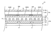
- FIG. 5 is a cross-sectional view of the display panel with a touch sensor 10 taken along line AA shown in FIG.
- the display panel with a touch sensor 10 includes a color filter substrate (counter substrate) 10a, an active matrix substrate 10b, and a liquid crystal layer sandwiched between the color filter substrate 10a and the active matrix substrate 10b. 10c, a shield electrode 10d disposed between the liquid crystal layer 10c and the color filter substrate 10a, and a sensor unit 10e formed on the surface of the color filter substrate 10a.
- the active matrix substrate 10 b includes a plurality of thin film transistors (TFTs) 17 and a plurality of TFTs 17 on a surface of a substrate 101 having transparency such as glass (a surface on the liquid crystal layer 10 c side). And a plurality of pixel electrodes 18 connected to each other. A comb-like common electrode 19 having a plurality of openings is disposed on the TFT 17 and the pixel electrode 18 with an insulating film 102 interposed therebetween.
- alignment films for horizontally aligning liquid crystal molecules are provided on the surface of the active matrix substrate 10b on the liquid crystal layer 10c side and the surface of the color filter substrate 10a on the liquid crystal layer 10c side. That is, the alignment film is disposed between the common electrode 19 and the liquid crystal layer 10c and between the shield electrode 10d and the liquid crystal layer 10c.
- a transparent conductive film excellent in transparency and conductivity such as ITO (IndiumInTin Oxide) or ZnO (Zinc Oxide) is used.
- ITO IndiumInTin Oxide
- ZnO Zinc Oxide
- a voltage of ⁇ 1 v to 0 v is applied to the common electrode 19
- a voltage of 0 v to 5 v is applied to the pixel electrode 18, for example.
- the liquid crystal layer 10c includes, for example, liquid crystal molecules having negative dielectric anisotropy (negative type).
- a lateral electric field (fringe field) is generated between the pixel electrode 18 and the common electrode 19 in the opening of the common electrode 19.
- the negative liquid crystal molecules are driven in the horizontal direction with respect to the substrate 101 in accordance with the lateral electric field.
- the negative liquid crystal molecules rotate so that the minor axis direction thereof is in the direction of the generated transverse electric field, that is, the major axis direction of the liquid crystal molecules is oriented in the direction perpendicular to the electric field.
- the color filter substrate 10a has R (red), G (green), and B (blue) at positions corresponding to the pixel electrodes 18 on the back surface (surface on the liquid crystal layer 10c side) of the transparent substrate 201 such as glass.
- Color filters 202R, 202G, and 202B corresponding to the respective colors are provided.
- the color filter substrate 10 a is provided with a black matrix 203 between adjacent color filters 202.
- the region where the R, G, B color filters 202R, 202G, 202B are arranged constitutes one sub-pixel, and one pixel is constituted by these three sub-pixels.
- a grounded shield electrode 10d is provided between the color filter 202 and the black matrix 203 and the liquid crystal layer 10c. More specifically, the shield electrode 10d is provided between the color filter 202 and the black matrix 203 and an alignment film (not shown) provided on the side of the color filter substrate 10a sandwiching the liquid crystal layer 10c. In this example, the distance between the shield electrode 10d and the common electrode 19 below the shield electrode 10d is about 3 ⁇ m.
- the material of the shield electrode 10d for example, a transparent conductive film such as ITO is used, and the film thickness is preferably about 10 nm, for example.
- the sheet resistance of the shield electrode 10d is preferably 1 k ⁇ / ⁇ or less. The lower the resistance between the shield electrode 10d and the ground (GND), the more the electric field perpendicular to the substrate surface is shielded by the shield electrode 10d. If the resistance between the shield electrode 10d and the ground (GND) is 1 k ⁇ / ⁇ or less, a vertical electric field due to the approach of a charged body up to about 10 kV can be shielded by the shield electrode 10d.
- the shield electrode 10d includes the dummy electrode 13, the liquid crystal layer 10c, and the like. It suffices to be provided so as to overlap at least the dummy electrode 13.
- the sensor unit 10 e includes a drive electrode 11, a detection electrode 12, and a dummy electrode 13. As shown in FIG. 3, drive electrodes 11 are arranged along the Y-axis direction on the surface of the color filter substrate 10a of the display panel 10 with a touch sensor.
- the drive electrode 11 includes a plurality of drive electrode pads 11a to 11m arranged in the Y-axis direction.
- a plurality of drive electrodes 11 are provided in the X-axis direction at a predetermined interval.
- the detection electrode 12 is a continuous electrode extended in the Y-axis direction.
- a plurality of detection electrodes 12 are provided in the X-axis direction at a predetermined interval.
- a transparent conductive film having excellent transparency and conductivity such as ITO or ZnO, is used.
- the drive electrode 11 is connected via a wiring 14 to a touch detection circuit (not shown) for controlling the detection of the touch position.
- the drive electrode 11 is supplied with a drive signal for detecting a touch position via a wiring 14 from a touch detection circuit (not shown).
- the detection electrode 12 is connected to a touch detection circuit (not shown), and outputs a signal corresponding to the capacitance between the detection electrode 12 and the drive electrode 11 to the touch detection circuit (not shown).
- the touch position is detected as follows.
- a drive signal is supplied from the touch detection circuit (not shown) to the drive electrode 11 to scan the drive electrode 11, and a signal indicating the capacitance between the drive electrode 11 and the detection electrode 12 is output from the detection electrode 12 to the touch detection circuit. (Not shown).
- the capacitance between the drive electrode 11 and the detection electrode 12 at the contact position changes.
- the touch detection circuit detects a touch position based on a capacitance in a state where the charged body is not approaching the display surface and a signal indicating the capacitance output from the detection electrode 12.
- dummy electrodes 13 are provided in regions other than the region where the drive electrode 11, the detection electrode 12, and the wiring 14 are provided.
- the dummy electrode 13 is provided in order to prevent occurrence of luminance unevenness due to a difference in transmittance between a region where the drive electrode 11, the detection electrode 12, and the wiring 14 are provided and a region other than this region.
- a transparent conductive film such as ITO or ZnO is used as in the drive electrode 11 and the detection electrode 12.
- the dummy electrode 13 is not connected to any of the drive electrode 11, the detection electrode 12, and the wiring 14, and is disposed in an electrically floating state.
- the shield electrode 10d is provided between the liquid crystal layer 10c and the color filter substrate 10a, the charged body approaches the region where the dummy electrode 13 is disposed. Even so, the vertical electric field is shielded by the shield electrode 10d. As a result, a vertical electric field is not generated between the dummy electrode 13 and the common electrode 19, and the alignment of the liquid crystal molecules in the liquid crystal layer 10c is not disturbed, so that display defects can be prevented.
- the shield electrode 10d is formed between the color filter substrate 10a and the liquid crystal layer 10c, and the touch sensor (the drive electrode 11 and the detection electrode 12) is formed on the surface of the color filter substrate 10a. .
- the thickness of the display panel 10 with a touch sensor can be reduced compared to the case where a shield electrode is provided on the color filter substrate 10a and the touch sensor is formed via an insulating film. .
- the shield electrode 10d is configured using a transparent conductive film.
- the shield electrode 10d is configured using, for example, a metal film formed in a mesh shape. Also good. For example, Cu, Al, Ta, or the like may be used as the material of the metal film.
- the liquid crystal layer 10c includes liquid crystal molecules (positive type) having positive dielectric anisotropy. May be.
- the shield electrode 10d is not provided, when a vertical electric field is generated in the region where the dummy electrode 13 is arranged, the liquid crystal molecules are aligned so that the major axis direction of the liquid crystal molecule is directed to the direction of the vertical electric field. .
- the pixel in which the liquid crystal molecules are arranged has a display defect.
- the shield electrode 10d is provided.
- FIGS. 6A and 6B are schematic diagrams illustrating the alignment state of negative liquid crystal molecules and positive liquid crystal molecules in a region where the shield electrode 10d is provided.
- the color filter substrate 10a and the sensor unit 10e are not shown, but the color filter substrate 10a and the sensor unit 10e are arranged on the shield electrode 10d as in FIG.
- a fringe electric field (broken line) is generated between the shield electrode 10 d and the pixel electrode 18.
- the liquid crystal molecules 101c are aligned in a substantially horizontal direction with respect to the substrate surface because the short axes are aligned along the fringe electric field.
- the liquid crystal molecules 102c are aligned so that the major axis direction thereof is oriented along the fringe electric field between the shield electrode 10d and the pixel electrode 18. That is, since the positive liquid crystal molecule 102c is more susceptible to the electric field in the direction perpendicular to the substrate surface than the negative liquid crystal molecule 101c, the liquid crystal molecule 102c is provided even if the shield electrode 10d is provided. The orientation of fluctuates in the vertical direction.
- FIG. 7 is an enlarged cross-sectional view of one sub-pixel portion of the display panel with a touch sensor 10 shown in FIG.
- a comb-like pixel electrode 181 and a common electrode 191 are provided on a substrate 101.
- the pixel electrodes 181 and the common electrodes 191 are alternately arranged with a horizontal separation with respect to the substrate surface.
- the liquid crystal molecules in the liquid crystal layer 10c are driven according to the lateral electric field generated between the adjacent pixel electrode 181 and the common electrode 191.
- the shield electrode 10d when a vertical electric field is generated between the dummy electrode 13 and the pixel electrode 181 or the common electrode 191 in the region where the dummy electrode 13 (see FIG. 5) is disposed, the shield electrode 10d The electric field in the vertical direction is shielded, and abnormal alignment of the liquid crystal layer 10c can be suppressed.
- the liquid crystal molecules in the liquid crystal layer 10c may be a positive type or a negative type.
- SYMBOLS 1 Display apparatus with a touch sensor, 10 ... Display panel with a touch sensor, 10a ... Color filter substrate, 10b ... Active matrix substrate, 10c ... Liquid crystal layer, 10e ... Sensor part, 10d ... Shield electrode, 11 ... Drive electrode, 11a- 11 m: drive electrode pad, 12: detection electrode, 13: dummy electrode, 14: wiring, 17: TFT, 18, 181: pixel electrode 18, 191 ... common electrode, 101, 201 ... substrate, 202 ... color filter, 203 ... Black matrix
Landscapes
- Physics & Mathematics (AREA)
- Engineering & Computer Science (AREA)
- Nonlinear Science (AREA)
- General Physics & Mathematics (AREA)
- General Engineering & Computer Science (AREA)
- Theoretical Computer Science (AREA)
- Chemical & Material Sciences (AREA)
- Crystallography & Structural Chemistry (AREA)
- Optics & Photonics (AREA)
- Human Computer Interaction (AREA)
- Mathematical Physics (AREA)
- Liquid Crystal (AREA)
- Microelectronics & Electronic Packaging (AREA)
Abstract
L'invention concerne une technique de réduction des défauts d'affichage causés par un champ électrique dans une direction perpendiculaire à un panneau d'affichage à cristaux liquides à commutation dans le plan sans compromettre des propriétés de conception d'un dispositif d'affichage équipé d'un capteur tactile, dans lequel un capteur tactile est formé dans le panneau d'affichage. L'invention concerne un dispositif d'affichage équipé d'un capteur tactile et comprenant un substrat de matrice active (10b) comportant des électrodes de pixels (18) et des électrodes partagées (19), un substrat de filtre de couleur (10a), et une couche de cristaux liquides (10c) excitée par des champs électriques transverses générés entre les électrodes de pixels (18) et les électrodes partagées (19). Un capteur tactile comportant des électrodes d'excitation (11) et des électrodes de détection (12) agencées de manière à être séparées l'une de l'autre dans la direction horizontale est installé du côté opposé du substrat de filtre de couleur (10a) depuis le substrat de matrice active (10b), et des électrodes factices (13) dans un état électriquement flottant sont installées entre les électrodes d'excitation (11) et les électrodes de détection (12). Une électrode de blindage (10d) connectée à la masse est installée entre les électrodes factices (13) et la couche de cristaux liquides (10c).
Applications Claiming Priority (2)
| Application Number | Priority Date | Filing Date | Title |
|---|---|---|---|
| JP2015040959 | 2015-03-03 | ||
| JP2015-040959 | 2015-03-03 |
Publications (1)
| Publication Number | Publication Date |
|---|---|
| WO2016140282A1 true WO2016140282A1 (fr) | 2016-09-09 |
Family
ID=56848942
Family Applications (1)
| Application Number | Title | Priority Date | Filing Date |
|---|---|---|---|
| PCT/JP2016/056487 Ceased WO2016140282A1 (fr) | 2015-03-03 | 2016-03-02 | Dispositif d'affichage équipé de capteur tactile |
Country Status (1)
| Country | Link |
|---|---|
| WO (1) | WO2016140282A1 (fr) |
Cited By (3)
| Publication number | Priority date | Publication date | Assignee | Title |
|---|---|---|---|---|
| JP2018060494A (ja) * | 2016-09-30 | 2018-04-12 | エルジー ディスプレイ カンパニー リミテッド | 有機発光表示装置及びそのタッチ感知方法 |
| CN108873436A (zh) * | 2018-07-23 | 2018-11-23 | 京东方科技集团股份有限公司 | 一种显示装置 |
| WO2022185368A1 (fr) * | 2021-03-01 | 2022-09-09 | シャープ株式会社 | Dispositif d'affichage |
Citations (5)
| Publication number | Priority date | Publication date | Assignee | Title |
|---|---|---|---|---|
| JP2008185785A (ja) * | 2007-01-30 | 2008-08-14 | Seiko Epson Corp | 入力機能付表示装置 |
| JP2008186714A (ja) * | 2007-01-30 | 2008-08-14 | Seiko Epson Corp | 入力機能付表示装置 |
| JP2010002958A (ja) * | 2008-06-18 | 2010-01-07 | Epson Imaging Devices Corp | 静電容量型入力装置および入力機能付き表示装置 |
| US20110169783A1 (en) * | 2010-01-08 | 2011-07-14 | Wintek Corporation | Touch Display Device |
| JP2014149387A (ja) * | 2013-01-31 | 2014-08-21 | Toppan Printing Co Ltd | 液晶表示装置及びカラーフィルタ基板 |
-
2016
- 2016-03-02 WO PCT/JP2016/056487 patent/WO2016140282A1/fr not_active Ceased
Patent Citations (5)
| Publication number | Priority date | Publication date | Assignee | Title |
|---|---|---|---|---|
| JP2008185785A (ja) * | 2007-01-30 | 2008-08-14 | Seiko Epson Corp | 入力機能付表示装置 |
| JP2008186714A (ja) * | 2007-01-30 | 2008-08-14 | Seiko Epson Corp | 入力機能付表示装置 |
| JP2010002958A (ja) * | 2008-06-18 | 2010-01-07 | Epson Imaging Devices Corp | 静電容量型入力装置および入力機能付き表示装置 |
| US20110169783A1 (en) * | 2010-01-08 | 2011-07-14 | Wintek Corporation | Touch Display Device |
| JP2014149387A (ja) * | 2013-01-31 | 2014-08-21 | Toppan Printing Co Ltd | 液晶表示装置及びカラーフィルタ基板 |
Cited By (6)
| Publication number | Priority date | Publication date | Assignee | Title |
|---|---|---|---|---|
| JP2018060494A (ja) * | 2016-09-30 | 2018-04-12 | エルジー ディスプレイ カンパニー リミテッド | 有機発光表示装置及びそのタッチ感知方法 |
| US10312297B2 (en) | 2016-09-30 | 2019-06-04 | Lg Display Co., Ltd. | Organic light emitting display device and touch sensing method for the same |
| CN108873436A (zh) * | 2018-07-23 | 2018-11-23 | 京东方科技集团股份有限公司 | 一种显示装置 |
| CN108873436B (zh) * | 2018-07-23 | 2021-04-06 | 京东方科技集团股份有限公司 | 一种显示装置 |
| WO2022185368A1 (fr) * | 2021-03-01 | 2022-09-09 | シャープ株式会社 | Dispositif d'affichage |
| US12524102B2 (en) | 2021-03-01 | 2026-01-13 | Sharp Kabushiki Kaisha | Display device |
Similar Documents
| Publication | Publication Date | Title |
|---|---|---|
| US10795514B2 (en) | Display device having touch detection function | |
| US10620730B2 (en) | Display device | |
| EP3296809B1 (fr) | Dispositif d'affichage à cristaux liquides | |
| US8582060B2 (en) | Liquid crystal display panel | |
| US20170017329A1 (en) | Liquid crystal display device | |
| US10152931B2 (en) | Display device | |
| JP2016167083A (ja) | 液晶表示装置 | |
| JP4946135B2 (ja) | 液晶表示素子 | |
| US10551682B2 (en) | Display device | |
| US10073311B2 (en) | Display device and electronic apparatus | |
| CN109991769B (zh) | 显示装置、显示装置的制造方法、及显示装置的检查方法 | |
| JP2009186869A (ja) | 液晶表示装置 | |
| JP5429776B2 (ja) | 液晶表示パネル | |
| JP4342696B2 (ja) | 液晶パネルの欠陥修正方法 | |
| JP5681269B2 (ja) | 液晶表示パネル | |
| US20150205170A1 (en) | Liquid crystal display | |
| WO2016140282A1 (fr) | Dispositif d'affichage équipé de capteur tactile | |
| WO2016163303A1 (fr) | Dispositif d'affichage à cristaux liquides doté d'un capteur tactile | |
| JP6045224B2 (ja) | 液晶表示装置 | |
| US11106316B2 (en) | Display panel having overlapping position detection lead-out lines disposed in different layers | |
| CN101435967B (zh) | 有源矩阵液晶显示装置 | |
| US11119614B2 (en) | Display panel | |
| WO2016136664A1 (fr) | Dispositif d'affichage à cristaux liquides à capteur tactile | |
| TWM464687U (zh) | 液晶顯示面板觸控結構 | |
| WO2018038038A1 (fr) | Dispositif d'affichage doté d'un panneau tactile |
Legal Events
| Date | Code | Title | Description |
|---|---|---|---|
| 121 | Ep: the epo has been informed by wipo that ep was designated in this application |
Ref document number: 16758975 Country of ref document: EP Kind code of ref document: A1 |
|
| NENP | Non-entry into the national phase |
Ref country code: DE |
|
| NENP | Non-entry into the national phase |
Ref country code: JP |
|
| 122 | Ep: pct application non-entry in european phase |
Ref document number: 16758975 Country of ref document: EP Kind code of ref document: A1 |