WO2016143241A1 - Dispositif d'entrée et appareil électrique - Google Patents
Dispositif d'entrée et appareil électrique Download PDFInfo
- Publication number
- WO2016143241A1 WO2016143241A1 PCT/JP2016/000377 JP2016000377W WO2016143241A1 WO 2016143241 A1 WO2016143241 A1 WO 2016143241A1 JP 2016000377 W JP2016000377 W JP 2016000377W WO 2016143241 A1 WO2016143241 A1 WO 2016143241A1
- Authority
- WO
- WIPO (PCT)
- Prior art keywords
- sensor
- recess
- pressure
- input device
- layer
- Prior art date
- Legal status (The legal status is an assumption and is not a legal conclusion. Google has not performed a legal analysis and makes no representation as to the accuracy of the status listed.)
- Ceased
Links
Images










Classifications
-
- G—PHYSICS
- G06—COMPUTING OR CALCULATING; COUNTING
- G06F—ELECTRIC DIGITAL DATA PROCESSING
- G06F1/00—Details not covered by groups G06F3/00 - G06F13/00 and G06F21/00
- G06F1/16—Constructional details or arrangements
- G06F1/1613—Constructional details or arrangements for portable computers
- G06F1/1633—Constructional details or arrangements of portable computers not specific to the type of enclosures covered by groups G06F1/1615 - G06F1/1626
- G06F1/1662—Details related to the integrated keyboard
- G06F1/1671—Special purpose buttons or auxiliary keyboards, e.g. retractable mini keypads, keypads or buttons that remain accessible at closed laptop
-
- G—PHYSICS
- G06—COMPUTING OR CALCULATING; COUNTING
- G06F—ELECTRIC DIGITAL DATA PROCESSING
- G06F3/00—Input arrangements for transferring data to be processed into a form capable of being handled by the computer; Output arrangements for transferring data from processing unit to output unit, e.g. interface arrangements
- G06F3/01—Input arrangements or combined input and output arrangements for interaction between user and computer
- G06F3/03—Arrangements for converting the position or the displacement of a member into a coded form
- G06F3/033—Pointing devices displaced or positioned by the user, e.g. mice, trackballs, pens or joysticks; Accessories therefor
- G06F3/0354—Pointing devices displaced or positioned by the user, e.g. mice, trackballs, pens or joysticks; Accessories therefor with detection of two-dimensional [2D] relative movements between the device, or an operating part thereof, and a plane or surface, e.g. 2D mice, trackballs, pens or pucks
- G06F3/03547—Touch pads, in which fingers can move on a surface
-
- G—PHYSICS
- G01—MEASURING; TESTING
- G01L—MEASURING FORCE, STRESS, TORQUE, WORK, MECHANICAL POWER, MECHANICAL EFFICIENCY, OR FLUID PRESSURE
- G01L1/00—Measuring force or stress, in general
-
- G—PHYSICS
- G06—COMPUTING OR CALCULATING; COUNTING
- G06F—ELECTRIC DIGITAL DATA PROCESSING
- G06F1/00—Details not covered by groups G06F3/00 - G06F13/00 and G06F21/00
- G06F1/16—Constructional details or arrangements
- G06F1/1613—Constructional details or arrangements for portable computers
- G06F1/1633—Constructional details or arrangements of portable computers not specific to the type of enclosures covered by groups G06F1/1615 - G06F1/1626
- G06F1/1684—Constructional details or arrangements related to integrated I/O peripherals not covered by groups G06F1/1635 - G06F1/1675
- G06F1/169—Constructional details or arrangements related to integrated I/O peripherals not covered by groups G06F1/1635 - G06F1/1675 the I/O peripheral being an integrated pointing device, e.g. trackball in the palm rest area, mini-joystick integrated between keyboard keys, touch pads or touch stripes
-
- G—PHYSICS
- G06—COMPUTING OR CALCULATING; COUNTING
- G06F—ELECTRIC DIGITAL DATA PROCESSING
- G06F3/00—Input arrangements for transferring data to be processed into a form capable of being handled by the computer; Output arrangements for transferring data from processing unit to output unit, e.g. interface arrangements
- G06F3/01—Input arrangements or combined input and output arrangements for interaction between user and computer
- G06F3/03—Arrangements for converting the position or the displacement of a member into a coded form
- G06F3/033—Pointing devices displaced or positioned by the user, e.g. mice, trackballs, pens or joysticks; Accessories therefor
- G06F3/038—Control and interface arrangements therefor, e.g. drivers or device-embedded control circuitry
-
- G—PHYSICS
- G06—COMPUTING OR CALCULATING; COUNTING
- G06F—ELECTRIC DIGITAL DATA PROCESSING
- G06F3/00—Input arrangements for transferring data to be processed into a form capable of being handled by the computer; Output arrangements for transferring data from processing unit to output unit, e.g. interface arrangements
- G06F3/01—Input arrangements or combined input and output arrangements for interaction between user and computer
- G06F3/03—Arrangements for converting the position or the displacement of a member into a coded form
- G06F3/041—Digitisers, e.g. for touch screens or touch pads, characterised by the transducing means
- G06F3/044—Digitisers, e.g. for touch screens or touch pads, characterised by the transducing means by capacitive means
- G06F3/0445—Digitisers, e.g. for touch screens or touch pads, characterised by the transducing means by capacitive means using two or more layers of sensing electrodes, e.g. using two layers of electrodes separated by a dielectric layer
-
- G—PHYSICS
- G06—COMPUTING OR CALCULATING; COUNTING
- G06F—ELECTRIC DIGITAL DATA PROCESSING
- G06F3/00—Input arrangements for transferring data to be processed into a form capable of being handled by the computer; Output arrangements for transferring data from processing unit to output unit, e.g. interface arrangements
- G06F3/01—Input arrangements or combined input and output arrangements for interaction between user and computer
- G06F3/03—Arrangements for converting the position or the displacement of a member into a coded form
- G06F3/041—Digitisers, e.g. for touch screens or touch pads, characterised by the transducing means
- G06F3/044—Digitisers, e.g. for touch screens or touch pads, characterised by the transducing means by capacitive means
- G06F3/0447—Position sensing using the local deformation of sensor cells
Definitions
- This technology relates to an input device and an electric device including a pressure sensor.
- pressure-sensitive sensors capable of electrostatically detecting input operations have been widely used in various electrical devices such as mobile PCs (Personal Computers) and tablet PCs.
- a pressure-sensitive sensor for electrical equipment a sensor that includes a capacitive element and has a configuration capable of detecting an operation position and a pressing force of an operator with respect to an input operation surface is known (for example, see Patent Document 1). ).
- An object of the present technology is to provide an input device and an electric device that can detect the pressing of the surface of the housing or the exterior body.
- the first technique is: A housing having a recess on the inner surface; A pressure-sensitive sensor provided in the recess, The pressure sensor is an input device that is fixed in the recess so that the sensing surface of the pressure sensor and the bottom surface of the recess are in contact with each other.
- the second technology is A housing having a recess on the inner surface; A plurality of pressure-sensitive sensors having a long shape provided in the recess, The plurality of pressure sensors are arranged spaced apart in the longitudinal direction of the pressure sensors, The plurality of pressure-sensitive sensors are input devices fixed in the recess so that the sensing surface of the pressure sensor and the bottom surface of the recess are in contact with each other.
- the third technology is A housing having a plurality of recesses extending in one direction on the inner surface; A plurality of long pressure-sensitive pressure sensors provided in a plurality of recesses, The plurality of recesses constitutes a plurality of rows, Each of the plurality of pressure sensors is an input device fixed in the plurality of recesses such that the sensing surface of the pressure sensor and the bottom surface of the recess are in contact with each other.
- the fourth technology is An exterior body having a recess on the inner surface and having rigidity; A pressure-sensitive sensor provided in the recess, The pressure sensor is an input device that is fixed in the recess so that the sensing surface of the pressure sensor and the bottom surface of the recess are in contact with each other.
- the fifth technology is A housing having a recess on the inner surface; A pressure-sensitive sensor provided in the recess, The pressure sensor is an electric device fixed in the recess so that the sensing surface of the pressure sensor and the bottom surface of the recess are in contact with each other.
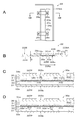
- FIG. 1A is a surface view illustrating an example of an appearance of an electric device according to the first embodiment of the present technology.
- FIG. 1B is a side view showing an example of the appearance of the electric device according to the first embodiment of the present technology.
- FIG. 1C is a back view illustrating an example of an appearance of the electric apparatus according to the first embodiment of the present technology.
- FIG. 2 is a block diagram illustrating an example of the configuration of the electrical device according to the first embodiment of the present technology.
- FIG. 3A is a plan view illustrating an example of a configuration of a sensing area.
- 3B is a cross-sectional view taken along line IIIB-IIIB in FIG. 3A.
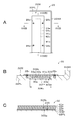
- FIG. 4A is a plan view illustrating an example of a sensing surface of the sensor.
- FIG. 1A is a surface view illustrating an example of an appearance of an electric device according to the first embodiment of the present technology.
- FIG. 1B is a side view showing an example of the appearance of the electric device
- FIG. 4B is a side view illustrating an example of a side surface of the sensor.
- FIG. 5A is a plan view showing an example of the configuration of the sensor.
- FIG. 5B is a cross-sectional view taken along the line VB-VB in FIG. 5A.
- FIG. 5C is a cross-sectional view taken along the line VC-VC in FIG. 5A.
- FIG. 6 is a cross-sectional view showing an example of the configuration of the sensor.
- FIG. 7A is a plan view showing an example of the configuration of the first and second electrodes.
- FIG. 7B is an enlarged plan view showing a part of FIG. 7A.
- FIG. 8 is a cross-sectional view showing an example of the operation of the sensor during an input operation.
- FIG. 8 is a cross-sectional view showing an example of the operation of the sensor during an input operation.
- FIG. 10A is a surface view illustrating an example of an appearance of an electric device according to a modification of the first embodiment of the present technology.
- FIG. 10B is a cross-sectional view illustrating an example of the configuration of the sensing area.
- FIG. 10C is a surface view illustrating an example of an appearance of an electric device according to a modification of the first embodiment of the present technology.
- FIG. 11A is a plan view illustrating an example of a configuration of a sensing area.
- FIG. 11B is a sectional view taken along line XIB-XIB in FIG. 11A.
- FIG. 11C and 11D are cross-sectional views illustrating a configuration example of the sensor.
- 12A to 12D are cross-sectional views illustrating configuration examples of the sensor.
- 13A to 13C are plan views showing a configuration example of the sensing area.
- FIG. 14A is a rear view illustrating an example of an appearance of an electric device according to the second embodiment of the present technology.
- FIG. 14B is a plan view illustrating an example of a configuration of a sensing area.
- FIG. 15 is a flowchart illustrating an example of the operation of the electrical device according to the second embodiment of the present technology.
- FIG. 16A and FIG. 16B are schematic diagrams for explaining an example of the operation of the electrical device according to the second embodiment of the present technology.
- FIG. 17A is a plan view illustrating an example of a configuration of a sensing area according to the third embodiment of the present technology.
- FIG. 17B is a cross-sectional view taken along line XVIIB-XVIIB in FIG. 17A.
- FIG. 17C is a cross-sectional view taken along line XVIIC-XVIIC in FIG. 17A.
- FIG. 18 is a cross-sectional view for explaining an example of the action of each member constituting the sensing area.
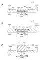
- 19A to 19C are cross-sectional views illustrating configuration examples of the sensing area in a modification example of the third embodiment of the present technology.
- FIG. 20A is a cross-sectional view illustrating an example of a configuration of a sensing area according to the fourth embodiment of the present technology.
- FIG. 20A is a cross-sectional view illustrating an example of a configuration of a sensing area according to the fourth embodiment of the present technology.
- 20B is a plan view showing an example of the configuration of the sensor.
- 20C is a cross-sectional view taken along line XXC-XXC in FIG. 20B.
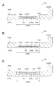
- 21A to 21D are plan views illustrating an example of a configuration of a sensing surface in a modification of the fourth embodiment of the present technology.
- FIG. 22A is a cross-sectional view illustrating an example of a configuration of a sensing area in a modification of the fourth embodiment of the present technology.
- FIG. 22B is a cross-sectional view illustrating an example of a configuration of a sensor according to a modified example of the fourth embodiment of the present technology.
- FIG. 23A is a cross-sectional view illustrating an example of a configuration of a sensing area according to the fifth embodiment of the present technology.
- FIG. 23B is a cross-sectional view showing an example of the configuration of the sensor.
- FIG. 24A is a cross-sectional view illustrating an example of a configuration of a sensing area according to the sixth embodiment of the present technology.
- FIG. 24B is a cross-sectional view illustrating a configuration example of a sensing area in a modified example of the sixth embodiment of the present technology.
- FIG. 25A is a cross-sectional view illustrating an example of a configuration of a sensing area according to the seventh embodiment of the present technology.
- FIG. 25B and 25C are cross-sectional views illustrating a configuration example of a sensing area in a modified example of the seventh embodiment of the present technology.
- FIG. 26A is a cross-sectional view illustrating a configuration example of a sensing area in a modification of the seventh embodiment of the present technology.
- FIG. 26B is a cross-sectional view illustrating a part of FIG. 26A in an enlarged manner.
- the electrical apparatus 10 is a so-called tablet computer, and includes a rigid casing 20, and the casing 20 includes a display device 11PL and the like.
- a camera module 11CM and the like are accommodated.
- the display device 11PL is provided on the surface 10Sa side of the electric device, and the camera module 11CM is provided on the back surface 10Sb side opposite to the display device 11PL.
- the front surface 10Sa and the rear surface 10Sb of the electrical device 10 have a rectangular shape having long and short sides when the surfaces are viewed from a vertical direction.
- Sensing areas 30Ra and 30Rb are provided at both ends in the longitudinal direction of the back surface 10Sb of the electric device 10, respectively.
- the sensing areas 30Ra and 30Rb are provided along the periphery of the back surface 10Sb, specifically, the short side of the back surface 10Sb.
- the sensing areas 30Ra and 30Rb have, for example, an elongated rectangular shape when viewed from a direction perpendicular to the back surface 10Sb.
- the user can operate the electric device 10 by pressing the sensing area 30Ra with an operator such as a finger.
- the housing 20 is made of a material having rigidity.
- a material having rigidity examples include metal, wood, polymer resin, and the like.
- the metal include simple substances such as aluminum, titanium, zinc, nickel, magnesium, copper, and iron, or alloys containing two or more of these.
- Specific examples of the alloy include stainless steel (Stainless Used Steel: SUS), aluminum alloy, magnesium alloy, titanium alloy, and the like.
- the housing 20 includes a first housing 21 that constitutes the front surface 10Sa side of the electric device, and a second housing 22 that constitutes the rear surface 10Sb side of the electric device.
- the first housing 21 has a large opening 21a, and the display portion of the display device 11PL is exposed from the opening 21a.
- a touch panel is provided on display device 11PL.
- the second housing 22 has a small opening 21a in the vicinity of the corner, and the lens portion of the camera module 11CM is exposed from the opening 22a.
- Examples of the display device 11PL include a liquid crystal display and an electroluminescence (EL) display, but are not limited thereto.
- Examples of the touch panel include a capacitive touch panel, but are not limited thereto.
- the electrical device 10 includes a host 11 that is a main body of the electrical device 10, sensors 30a and 30b, and controller ICs (Integrated Circuits) 12a and 12b. Prepare.
- Sensors 30a and 30b are electrostatic pressure sensors.
- the controller ICs 12a and 12b detect a change in capacitance according to the pressing (operation) of the sensing areas 30Ra and 30Rb, and output a capacitance distribution corresponding to the change, that is, a pressure-sensitive distribution, to the host 11.
- the host 11 includes the above-described display device 11PL, camera module 11CM, and the like, and executes various processes according to the operation of a touch panel provided on the display device 11PL. For example, the host 11 executes processing such as displaying images and character information on the display device 11PL and moving a cursor displayed on the display device 11PL. Further, the host 11 executes shooting of still images and moving images by the camera module 11CM.
- the host 11 controls the operation of the electrical equipment based on the detection results of the sensors 30a and 30b. Specifically, a predetermined process is performed based on the pressure distribution supplied from each of the sensors 30a and 30b. For example, when a predetermined pressure or higher is applied to the sensing areas 30Ra and 30Rb, or when a predetermined pressure or higher is applied to the sensing areas 30Ra and 30Rb for a predetermined time or longer, the sleep mode (energy saving mode) of the electric device 10 is released. Note that the processing of the host 11 described above is specifically executed by a control unit included in the host 11.
- the second housing 22 constituting the back surface 10Sb side of the electric device 10 includes a plate-like main surface portion 22PL and a peripheral wall portion 22WA provided on the periphery thereof.
- the inner side surface 22SI of the second housing 22 has a rectangular shape having a long side and a short side.
- the second housing 22 has recesses 23a and 23b at positions on the back side of the sensing areas 30Ra and 30Rb. Specifically, the recesses 23a and 23b are respectively provided at both ends in the longitudinal direction of the inner side surface 22SI. The recesses 23a and 23b extend in the short direction of the inner side surface 22SI. Specifically, the recesses 23a and 23b are extended along the short side of the inner surface 22SI. The recesses 23a and 23b have substantially the same size and shape as the sensing areas 30Ra and 30Rb, respectively.
- the bottom surface 23S of the recesses 23a and 23b has a planar shape.
- the sensor 23a and a back plate 24a as a fixing member are accommodated in the recess 23a.
- the sensor 30a is electrically connected to a PCBA (Printed Circuit Board Assembly) 13a via an FPC (Flexible printed circuit) 14a.
- the above-described controller IC 12a is mounted on the PCBA 13a.
- a sensor 30b and a back plate 24b as a fixing member are accommodated in the recess 23b.
- the sensor 30b is electrically connected to the PCBA 13b via the FPC 14b.
- the above-described controller IC 12b is mounted on the PCBA 13b.
- the inner surface 22SI of the second housing 22 may further be provided with a recess for accommodating the FPC 14a, and this recess may be connected to the recess 23a and integrated.
- a recess for accommodating the FPC 14b may be further provided on the inner side surface 22SI of the second housing 22, and the recess may be integrated with the recess 23b.
- the sensor 30a is a pressure-sensitive sensor that can electrostatically detect the pressing (input operation) of the sensing surface 30Sa.
- the sensor 30a is a long sheet having a sensing surface 30Sa as a first surface and a back surface 30Sb as a second surface.
- the sensing surface 30Sa and the back surface 30Sb have a rectangular shape when viewed from the direction perpendicular to the respective surfaces.
- the sensor 30 is preferably easier to deform than the back plate 24a.
- the Young's modulus Ea of the sensor 30a is preferably smaller than the Young's modulus Eb of the back plate 24a (Ea ⁇ Eb). This is because the detection sensitivity of the sensing area 30Ra can be improved.
- the sensor 30a preferably has a plurality of convex portions 30TP on at least one of the sensing surface 30Sa and the back surface 30Sb, and both the sensing surface 30Sa and the back surface 30Sb. It is more preferable to have a plurality of convex portions 30TP.
- the sensor 30a is provided with a plurality of convex portions 30TP on one of the sensing surface 30Sa and the back surface 30Sb, from the viewpoint of improving the detection sensitivity of the sensing area 30Ra, a plurality of sensing surfaces 30Sa facing the bottom surface 23S of the concave portion 23a are provided. It is preferable to provide the convex portion 30TP.
- 4A and 4B show the configuration of a sensor 30a having a plurality of convex portions 30TP on both the sensing surface 30Sa and the back surface 30Sb.
- the sensor 30a includes a plurality of sensor units 30D, and the plurality of sensor units 30D are one-dimensionally arranged at predetermined intervals in the longitudinal direction of the sensor 30a.
- the plurality of convex portions 30TP disposed on the sensing surface 30Sa are respectively disposed on the center positions of the plurality of sensor portions 30D.
- the plurality of convex portions 30TP disposed on the back surface 30Sb are also disposed on the center positions of the plurality of sensor portions 30D.
- the convex portion 30TP When the sensor 30a is viewed from a direction perpendicular to the sensing surface 30Sa, the convex portion 30TP has an elongated shape extending in the longitudinal direction of the sensing surface 30Sa, for example, as shown in FIG. 4A.
- the shape of the convex portion 30TP is not limited to this, but a cone shape, a column shape (for example, a columnar shape, a polygonal column shape), a needle shape, a shape of a part of a sphere (for example, a hemispherical shape), an ellipsoidal shape, etc.
- Some shapes for example, semi-ellipsoidal shape), polygonal shapes, and the like may be used.
- the sensor 30a is accommodated in the recess 23a so that the sensing surface 30Sa of the sensor 30a and the bottom surface 23S of the recess 23a are opposed to and in contact with each other. Therefore, the sensing surface 30Sa becomes a sensing surface that detects a pressure on the sensing area 30Ra.
- the back plate 24a has a U-shaped cross section.
- the back plate 24a is fitted in the recess 23a of the second casing 22 so as to accommodate the sensor 30a in the recess and to cover the back surface 30Sb of the sensor 30a.
- the back plate 24a fixes the sensor 30a in the recess 23a so that the contact between the sensing surface 30Sa of the sensor 30a and the bottom surface 23S of the recess 23a is maintained.
- the back plate 24a is a pressing member that fixes the sensor 30a in the recess 23a by pressing the sensing surface 30Sa of the sensor 30a against the bottom surface 23S of the recess 23a. It is preferable.
- the back plate 24a is made of, for example, a polymer resin or a metal.
- the spring plate 27a may have a laminated structure of a polymer resin layer and a metal layer.
- Examples of the polymer resin include those similar to the base materials 31a and 35a.
- the polymer resin of the base materials 31a and 35a will be described later.
- As a metal the thing similar to the housing
- the thickness D of the second housing 22 at the bottom surface 23S of the recess 23a is preferably thin from the viewpoint of improving the detection sensitivity of the sensing area 30Ra.
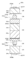
- the ratio (W / D) of the width W of the recess 23a to the thickness D of the second housing 22 on the bottom surface 23S of the recess 23a is preferably 20 or more, more preferably 23 or more. When the ratio (W / D) is 20 or more, the detection sensitivity of the sensing area 30Ra can be improved.
- the sensor 30a includes a reference electrode layer (hereinafter referred to as “REF electrode layer”) 31, a space layer 32, a sensor layer 33, a space layer 34, and a conductive layer as a conductive layer. And a REF electrode layer 35 as a layer.
- REF electrode layer a reference electrode layer
- the main surface which becomes the sensing surface side among both main surfaces of the sensor 30a and its component (component member) may be referred to as the front surface, and the main surface on the opposite side may be referred to as the back surface.
- the REF electrode layer 31 is provided on the back side of the sensor layer 33, and the REF electrode layer 35 is provided on the front side of the sensor layer 33.
- the REF electrode layers 31 and 35 are provided on both sides of the sensor layer 33 in this manner, it is possible to prevent external noise (external electric field) from entering the sensor 30a.
- a space layer 32 is provided between the front surface of the REF electrode layer 31 and the back surface of the sensor layer 33.
- a space layer 34 is provided between the front surface of the sensor layer 33 and the back surface of the REF electrode layer 35.
- the REF electrode layer 31 constitutes the back surface of the sensor 30a.
- the REF electrode layer 35 constitutes the sensing surface 30Sa of the sensor 30a.
- the REF electrode layers 31 and 35 are connected to a ground potential, for example.
- the REF electrode layer 31 is a conductive base material having rigidity or flexibility, and includes a base material 31a and a conductive layer 31b provided on the back surface of the base material 31a as shown in FIG.
- the REF electrode layer 31 is provided so that the base 31 a side faces the back surface of the sensor layer 33.
- the REF electrode layer 31 may have higher bending rigidity than the sensor layer 33, the REF electrode layer 35, and the like, for example, and may function as a support plate for the sensor 30a.
- the REF electrode layer 35 is a conductive base material having flexibility, and includes a base material 35a and a conductive layer 35b provided on the back surface of the base material 35a, as shown in FIG.
- the REF electrode layer 35 can be deformed according to the pressing of the sensing surface 30Sa of the sensor 30a.
- the REF electrode layer 35 is provided so that the conductive layer 35 b side faces the surface of the sensor layer 33.
- the base materials 31a and 35a have, for example, a film shape or a plate shape.
- the film includes a sheet.
- a material of the base materials 31a and 35a for example, a polymer resin or glass can be used.
- polymer resin examples include polyethylene terephthalate (PET), polyethylene naphthalate (PEN), polycarbonate (PC), acrylic resin (PMMA) polyimide (PI), triacetyl cellulose (TAC), polyester, polyamide (PA), Aramid, polyethylene (PE), polyacrylate, polyether sulfone, polysulfone, polypropylene (PP), diacetyl cellulose, polyvinyl chloride, epoxy resin, urea resin, urethane resin, melamine resin, cyclic olefin polymer (COP), norbornene A thermoplastic resin etc. are mentioned.
- the conductive layers 31b and 35b only have to have electrical conductivity.
- an inorganic conductive layer containing an inorganic conductive material an organic conductive layer containing an organic conductive material, an inorganic conductive material, and an organic conductive material
- An organic-inorganic conductive layer containing both of them can be used.
- the inorganic conductive material examples include metals and metal oxides.
- the metal is defined to include a semi-metal.
- the metal include aluminum, copper, silver, gold, platinum, palladium, nickel, tin, cobalt, rhodium, iridium, iron, ruthenium, osmium, manganese, molybdenum, tungsten, niobium, tantel, titanium, bismuth, antimony,
- a metal such as lead, or an alloy thereof may be used, but is not limited thereto.
- the metal oxide examples include indium tin oxide (ITO), zinc oxide, indium oxide, antimony-added tin oxide, fluorine-added tin oxide, aluminum-added zinc oxide, gallium-added zinc oxide, silicon-added zinc oxide, and zinc oxide- Examples thereof include, but are not limited to, a tin oxide system, an indium oxide-tin oxide system, and a zinc oxide-indium oxide-magnesium oxide system.
- ITO indium tin oxide
- zinc oxide indium oxide
- indium oxide antimony-added tin oxide
- fluorine-added tin oxide aluminum-added zinc oxide
- gallium-added zinc oxide gallium-added zinc oxide
- silicon-added zinc oxide silicon-added zinc oxide
- zinc oxide- Examples thereof include, but are not limited to, a tin oxide system, an indium oxide-tin oxide system, and a zinc oxide-indium oxide-magnesium oxide system.
- organic conductive materials include carbon materials and conductive polymers.
- the carbon material include, but are not limited to, carbon black, carbon fiber, fullerene, graphene, carbon nanotube, carbon microcoil, and nanohorn.
- the conductive polymer for example, substituted or unsubstituted polyaniline, polypyrrole, polythiophene, and one or two (co) polymers selected from these can be used, but are not limited thereto. is not.
- the sensor layer 33 is provided between the REF electrode layer 31 and the REF electrode layer 35, changes in the distance from the REF electrode layer 35 on the sensing surface (operation surface) 30Sa side, and the REF electrode layer on the back surface 30Sb side. It is possible to electrostatically detect a change in the distance to 31.
- the sensor layer 33 includes a plurality of sensor units 22D, and the plurality of sensor units 22D are arranged at a distance between the sensor layer 33 and the REF electrode layer 31 and a distance between the sensor layer 33 and the REF electrode layer 35. The capacitance that changes in response is detected.
- the plurality of sensor units 22D are arranged at equal intervals in the longitudinal direction of the sensor 30a.
- the sensor layer 33 is an electrostatic capacitance type sensor layer, and as shown in FIG. 6, the base material 33a and one or a plurality of first electrodes (Y electrodes) 33EY provided on the back surface of the base material 33a. And the insulating layer 33b covering the one or more first electrodes 33EY, the adhesive layer 33c provided on the surface side of the base material 33a, and the surface of the base material 33a via the adhesive layer 33c.
- the substrate 33d includes one or a plurality of second electrodes (X electrodes) 33EX provided on the back surface side of the substrate 33d.
- the plurality of sensor units 30D are configured by intersections of one or more first electrodes 33EY and one or more second electrodes 33EX.
- first and second electrodes 33EY and 33EX will be described with reference to FIGS. 7A and 7B.
- the plurality of sensor units 30D are configured by intersections of four first electrodes 33EY and five second electrodes 33EX.
- the first electrode 33EY includes an electrode line portion 33EYa extending in the longitudinal direction of the sensor 30a and a lead line portion 33EYb drawn from one end of the electrode line portion 33EYa.
- the electrode line portion 33EYa has, for example, a linear shape.
- the second electrode 33EX includes two unit electrode bodies 33EXa and a connection line portion 33EXb that connects these two unit electrode bodies 33EXa.
- the unit electrode body 33EXa has, for example, a comb shape, a ladder shape, or a mesh shape.
- a plurality of unit electrode bodies 33EXa are provided on the electrode wire portion 33EYa extending in the longitudinal direction of the sensor 30a.
- a sensor unit 30D is configured by an overlapping portion of the electrode line portion 33EYa and the unit electrode body 33EXa.
- the plurality of unit electrode bodies 33EXa form one row extending in the longitudinal direction of the sensor 30a.
- the four electrode wire portions 33EYa are extended in the direction of the row so as to overlap the plurality of unit electrode bodies 33EXa in the thickness direction of the sensor 30a.
- the two electrode wire portions 33EYa provided in parallel extend from one end of the row to almost the center with a predetermined interval.
- the remaining two electrode wire portions 33EYa provided in parallel are extended from the other end of the row to almost the center, separated by a predetermined distance.
- the unit electrode bodies 33EXa located symmetrically with respect to the center of the row are electrically connected to each other by the connection line portion 33EXb.
- the first and second electrodes 33EY and 33EX are wired as described above, the first and second electrodes 33EY and 33EX can be efficiently wired. Further, the FPC 14 a can be easily provided at any position on the long side of the long sensor layer 33.
- FIG. 7 shows an example in which the FPC 14 a is provided at the center of the long side of the long sensor layer 33.
- the electrode line portions 33EYa adjacent in the short direction of the sensor 30a are electrically connected by a plurality of connecting portions 33EYc. Thereby, even if one of the two electrode wire portions 33EYa provided in parallel is disconnected, the function as the sensor 30a is maintained. Therefore, the durability of the sensor 30a is improved.
- the connecting portion 33EYc is preferably provided between the unit electrode bodies 33EXa adjacent in the longitudinal direction of the sensor 30a.
- the base materials 33a and 33d are the same as the base materials 31a and 35a described above.
- an ultraviolet curable resin for example, an ultraviolet curable resin, a thermosetting resin, an insulating resist, a metal compound, or the like can be used.
- polyacrylates PVA (polyvinyl alcohol), PS (polystyrene), polyimide, polyester, epoxy, polyvinyl phenol, polyvinyl resin material such as an alcohol, SiO 2, SiNx, SiON, Al 2 O 3, Ta 2 Metal compounds such as O 5 , Y 2 O 3, HfO 2 , HfAlO, ZrO 2 , and TiO 2 can be used.
- the adhesive layer 33c is made of, for example, an insulating adhesive or a double-sided adhesive tape.
- the adhesive for example, one or more selected from the group consisting of an acrylic adhesive, a silicone adhesive, a urethane adhesive, and the like can be used.
- adhesion pressure sensitivehesadhesion
- the adhesive layer is regarded as a kind of adhesive layer.
- the space layer 32 includes a frame 32a as a peripheral structure and a plurality of structures 32b.
- the frame 32 a and the plurality of structures 32 b are provided between the REF electrode layer 31 and the sensor layer 33, and are separated from the REF electrode layer 31 and the sensor layer 33.
- the plurality of structures 32b are one-dimensionally arranged at predetermined intervals in the longitudinal direction of the sensor 30a.
- the structure 32b is provided at a position between adjacent sensor units 30D or at a position of the sensor unit 30D.
- 5A to 5C show examples of the latter arrangement.
- the structure 32b is provided with the structure part 32c and the junction part 32d, as shown in FIG.
- the structure portion 32c is, for example, a cone shape, a column shape (for example, a columnar shape or a polygonal column shape), a needle shape, a partial shape of a spherical body (for example, a hemispherical shape), or a partial shape of an ellipsoid (for example, a semi-elliptical shape). ), Polygonal shapes, and the like, but are not limited to these shapes, and other shapes may be adopted.
- the joint part 32d is provided on the structure part 32c, and the structure part 32c and the REF electrode layer 31 are bonded via the joint part 32d.
- a material of the structural part 32c for example, a resin material having an insulating property is used.
- a photocurable resin such as an ultraviolet curable resin can be used.
- an adhesive resin material or the like is used as the material of the joint portion 32d.
- the structure 32b is not limited to the structure in which the structure 32c and the joint 32d are separated as described above, and the structure 32c and the joint 32d are integrally formed in advance. You may make it employ
- a material of the structure 32b for example, a material capable of realizing both functions of the structure portion 32c and the joint portion 32d is selected.
- the frame 32a is provided between the REF electrode layer 31 and the sensor layer 33 continuously or discontinuously along the peripheral edge thereof.
- a material of the frame 32a for example, a resin material having adhesiveness and insulating properties is used.
- the frame body 32 a has a function of a joining part for joining the REF electrode layer 31 and the sensor layer 33 in addition to a function as a separating part for separating the REF electrode layer 31 and the sensor layer 33. .
- the space layer 34 includes a frame 34a as a peripheral structure and a plurality of structures 34b.
- the frame 34 a and the plurality of structures 34 b are provided between the REF electrode layer 35 and the sensor layer 33, and are separated from the REF electrode layer 35 and the sensor layer 33.
- the plurality of structures 34b are one-dimensionally arranged at predetermined intervals in the longitudinal direction of the sensor 30a. When the sensor 30a is viewed from a direction perpendicular to the sensing surface 30Sa, the structure 34b is provided at a position between adjacent sensor units 30D or at a position of the sensor unit 30D. 5A to 5C show an example of the former arrangement.
- the positions of the structures 32b and 34b are provided so as not to overlap in the thickness direction of the sensor 30a. That is, when the structure 32b is provided at a position between the adjacent sensor units 30D, the structure 34b is provided at the position of the sensor unit 30D. On the other hand, when the structure 32b is provided at the position of the sensor unit 30D, the structure 34b is provided at a position between the adjacent sensor units 30D.
- the structure 34 b includes a structure 34 c and a joint 34 d.
- the structure 34c is, for example, a cone shape, a column shape (for example, a columnar shape or a polygonal column shape), a needle shape, a partial shape of a sphere (for example, a hemispherical shape), or a partial shape of an ellipsoid (for example, a semi-elliptical shape). ), Polygonal shapes, and the like, but are not limited to these shapes, and other shapes may be adopted.
- the joint 34d is provided on the structure 34c, and the structure 34c and the REF electrode layer 35 are bonded to each other through the joint 34d.
- a material of the structure portion 34c for example, a resin material having insulating properties is used.
- a photocurable resin such as an ultraviolet curable resin can be used.
- an adhesive resin material or the like is used as the material of the bonding portion 34d.
- the structure 34b is not limited to the structure in which the structure 34c and the joint 34d are separated as described above, and the structure 34c and the joint 34d are integrally formed in advance. You may make it employ
- the material of the structure 34b for example, a material capable of realizing both functions of the structure 34c and the joint 34d is selected.
- the frame 34a is provided between the REF electrode layer 35 and the sensor layer 33 continuously or discontinuously along the peripheral edge thereof.
- a material of the frame 34a for example, a resin material having adhesiveness and insulating properties is used.
- the frame body 34 a has a function of a joining part that joins between the REF electrode layer 35 and the sensor layer 33 in addition to a function as a separating part that separates the REF electrode layer 35 and the sensor layer 33. .
- the sensing area 30Ra When the sensing area 30Ra is pressed (input operation) by an operator such as a finger, the casing 20 of the sensing area 30Ra is slightly deformed, and the sensing surface 30Sa of the sensor 30a is pressed by this deformation. Thereby, the distance between the REF electrode layer 31 and the sensor layer 33 and the distance between the REF electrode layer 35 and the sensor layer 33 change. The plurality of sensor units 30D included in the sensor layer 33 detect this change electrostatically. This detection result is output to the host 11 as a capacitance distribution, that is, a pressure distribution, via the controller IC 12a.
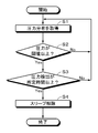
- step S1 the host 11 which is the main body of the electric device 10 acquires the pressure distribution of the sensors 30a and 30b via the controller ICs 12a and 12b.
- step S2 based on the acquired pressure distribution, the host 11 determines whether or not pressure equal to or higher than the threshold is applied to the sensors 30a and 30b via the sensing areas 30Ra and 30Rb.
- step S3 the host 11 determines whether pressure detection equal to or higher than the threshold continues for a predetermined time or more. On the other hand, if it is determined in step S2 that no pressure equal to or higher than the threshold is applied to the sensors 30a and 30b, the host 11 returns the process to step S1.
- step S3 If it is determined in step S3 that the pressure detection above the threshold has continued for a predetermined time or longer, the host 11 cancels the sleep process of the electrical device 10 in step S4. On the other hand, if it is determined in step S3 that the pressure detection is not longer than the predetermined time, the host 11 returns the process to step S1.
- the electrical device 10 includes a second housing 22 having recesses 23a and 23b on the inner surface 22SI, and a press applied to the outer surface of the second housing 22 provided in the recesses 23a and 23b.
- Pressure-sensitive sensors 30a and 30b are fixed in the recesses 23a and 23b so that the sensing surfaces 30Sa of the sensors 30a and 30b are in contact with the bottom surfaces 23S of the recesses 23a and 23b.
- the sensing areas 30Ra and 30Rb on the back side of the bottom surface 23S of the recesses 23a and 23b are pressed by an operator such as a finger, the bottom surfaces 23S of the recesses 23a and 23b are slightly bent, and the bottom surfaces 23S of the recesses 23a and 23b. As a result, the sensing surfaces 30Sa of the sensors 30a and 30b are pressed. Therefore, the sensors 30a and 30b can detect pressure applied to the sensing areas 30Ra and 30Rb on the back side of the bottom surface 23S of the recesses 23a and 23b.
- the entire housing 20 is made of a rigid material
- the sensing areas 30Ra and 30Rb of the housing 20 or the sensing areas 30Ra and 30Rb are not included.
- the part to include may be made of a material having rigidity.
- the pressure-sensitive sensor is not limited to the sensors 30a and 30b in the first embodiment described above, and a general sheet-shaped pressure-sensitive sensor or the like can also be used. However, from the viewpoint of improving the detection sensitivity of the sensing areas 30Ra and 30Rb, it is preferable to use the sensors 30a and 30b in the first embodiment described above.
- the REF electrode layers 31 and 35 may be constituted only by the conductive layers 31b and 35b, respectively. In this case, an insulating layer may be provided on the surfaces of the conductive layers 31b and 35b.
- sensing areas 30Ra and 30Rb may be provided at both ends in the longitudinal direction of the surface 10Sa of the electric device 10, respectively.
- the sensing areas 30Ra and 30Rb may be provided at both ends in the longitudinal direction of the back surface 10Sb of the electrical device 10, or may not be provided on the back surface 10Sb.
- the sensing surface 30Sa of the sensor 30a and the bottom surface 23S of the recess 23a of the second housing 22 may be bonded together with an adhesive layer 25a.
- the back plate 24a is preferably provided as shown in FIG. 11B, but the back plate 24a may be omitted.
- the adhesive layer 25a is the same as the adhesive layer 33c in the first embodiment, for example.
- the adhesive layer 25a is made of, for example, an insulating adhesive or a double-sided adhesive tape.
- the sensing areas 30Ra and 30Rb are provided on the back surface 10Sb of the electric device 10.
- the position of the sensing areas 30Ra and 30Rb can be easily achieved by touching one or a plurality of convex portions 26a and 26b with a finger or the like. Can grasp.
- One or a plurality of convex portions 26a, 26b are preferably provided on the sensor portion 30D included in the sensors 30a, 30b. This is because the detection sensitivity of the sensing areas 30Ra and 30Rb can be improved.
- one or a plurality of spring plates 27a as fixing members for fixing the back plate 24a may be provided.
- the spring plate 27a is fixed to the inner side surface 22SI of the second housing 22 by, for example, one or a plurality of screw members 28a.
- the spring plate 27a is preferably fixed by pressing the back plate 24a against the back surface 30Sb of the sensor 30a. This is because the detection sensitivity of the sensing area 30Ra can be improved.
- the spring plate 27a is made of, for example, polymer resin or metal.
- the spring plate 27a may have a laminated structure of a polymer resin layer and a metal layer.
- Examples of the polymer resin include those similar to the base materials 31a and 35a in the first embodiment.
- As a metal the thing similar to the housing
- the space layer 32 may not be provided with a structure, and the structure 34b may be provided only in the space layer 34.
- the structure 34b is provided at a position between the adjacent sensor units 30D or the position of the sensor unit 30D.
- FIG. 12A shows an example of the former arrangement.
- the space layer 34 may not be provided with a structure, and only the space layer 32 may be provided with a structure 32b.
- the structure 32b is provided at a position between the adjacent sensor units 30D or a position of the sensor unit 30D.
- FIG. 12B an example of the latter arrangement is shown.
- the spatial layer may not be provided between the REF electrode layer 31 and the sensor layer 33, and the REF electrode layer 31 and the sensor layer 33 may be in contact with each other.
- the structure 34b is provided at a position between the adjacent sensor units 30D when the sensor 30a is viewed from a direction perpendicular to the sensing surface 30Sa.
- the structure 34b is not provided between the REF electrode layer 35 and the sensor layer 33, and the REF electrode layer 35 and the sensor layer 33 are separated only by the frame 34a. You may do it.
- the space layer may not be provided between the REF electrode layer 35 and the sensor layer 33, and the REF electrode layer 35 and the sensor layer 33 may be in contact with each other.
- the structure 34b is provided at a position between the adjacent sensor units 30D when the sensor 30a is viewed from a direction perpendicular to the sensing surface 30Sa.
- the structural body 32b is not provided between the REF electrode layer 31 and the sensor layer 33, and the REF electrode layer 31 and the sensor layer 33 are separated only by the frame body 32a. You may do it.
- a plurality of long pressure-sensitive sensors 30a may be provided in the recess 23a.
- the plurality of pressure sensitive sensors 30a are arranged in the concave portion 23a apart from each other in the longitudinal direction of the pressure sensitive sensor 30a. This is because even when the pressure sensor 30a expands and contracts due to a temperature change in the electrical device 10, it is possible to suppress the occurrence of positional displacement or peeling of the pressure sensor 30a.
- the plurality of pressure-sensitive sensors 30b having a long shape have the same configuration as that of the pressure-sensitive sensor 30a.
- a plurality of recesses 23a extending in the short direction of the inner side surface 22SI are provided at one end in the longitudinal direction of the inner side surface 22SI, and the plurality of recesses 23a constitute a plurality of rows. You may do it.
- a plurality of pressure-sensitive sensors having a long shape may be provided in each of the plurality of recesses 23a. In this case, it is possible to suppress displacement and peeling of the pressure-sensitive sensor 30a due to expansion and contraction. Further, by arranging a plurality of columns of sensors 30a and assigning a function for each column, it may be a matrix node and a gesture operation may be realized.
- the plurality of recesses 23a form a plurality of rows, as shown in FIG. 13C, the plurality of rows are in a direction orthogonal to the extending direction of the recesses 23a (longitudinal direction of the inner surface 22SI).
- the adjacent recesses 23a may be arranged so as to be shifted stepwise in the extending direction of the recesses 23a. 13A to 13C, the back plate 24a is not shown.
- the example in which the plurality of convex portions 30TP are provided on at least one of the sensing surface 30Sa and the back surface 30Sb of the sensor 30a has been described.
- the sensing surface 30Sa of the sensor 30a and the bottom surface 23S of the concave portion 23a A plurality of convex portions may be provided on at least one of them.
- a plurality of convex portions may be provided on at least one of the sensing surface 30Sa of the sensor 30b and the bottom surface 23S of the concave portion 23b.
- the example in which the plurality of convex portions 30TP are provided on at least one of the sensing surface 30Sa and the back surface 30Sb of the sensor 30a has been described. However, at least one of the sensing surface 30Sa and the back surface 30Sb of the sensor 30a.
- One convex portion may be provided. In this case, the convex portion 30TP is provided at the center position in the short side direction (width direction) of the sensor 30a and extends in the longitudinal direction of the sensor 30a.
- the example in which the sleep mode is canceled by pressing the sensing areas 30Ra and 30Rb has been described.
- the operation of other electrical devices is performed by pressing the sensing areas 30Ra and 30Rb.
- the output sound level may be adjusted, the screen brightness may be adjusted, the sleep operation may be performed, and the like.
- the host 11 determines whether or not the pressure detection exceeding the threshold value continues for a predetermined time or more, and based on the result of this determination, the operation of the predetermined electric device (sleep release) is executed.
- the detection operation of the electric device 10 is not limited to this example.
- the host 11 determines whether or not a pressure equal to or greater than a threshold value has been detected a predetermined number of times, and when a pressure equal to or greater than the threshold value is detected a predetermined number of times or more, the operation of a predetermined electric device is executed. Also good.
- the host 11 determines whether or not a pressure equal to or higher than the threshold is detected within a predetermined width, and when a pressure equal to or higher than the threshold is detected within a predetermined width, the operation of a predetermined electric device is executed. It may be.
- the electrical device is a tablet computer
- various electrical devices having an exterior body such as a housing
- Applicable for example, mobile phones such as personal computers and smartphones, televisions, cameras, game machines, navigation systems, e-books, electronic dictionaries, portable music players, wearable terminals such as smart watches and head-mound displays, radios, electric tools, refrigerators, air conditioners, It can also be applied to wearable devices, stereos, water heaters, microwave ovens, dishwashers, washing machines, dryers, lighting devices, toys, medical devices, robots, and the like.
- electric devices include so-called electronic devices.
- the housing is an example of a rigid exterior body.
- the present technology is not limited to electrical devices, and can be applied to various devices other than electrical devices.
- the present invention can be applied to buildings such as houses, building members, vehicles, furniture such as tables and desks, manufacturing apparatuses, and analytical instruments.
- building members include paving stones, wall materials, floor tiles, floor boards, and the like.
- the vehicle include a vehicle (for example, an automobile, a motorcycle, etc.), a ship, a submarine, a railway vehicle, an aircraft, a spacecraft, an elevator, a play equipment, and the like.
- sensing areas 30Rc and 30Rd are provided at both ends in the short direction of the back surface 10Sb of the electric device 10M.
- the sensing areas 30Rc and 30Rd are provided along the long side of the back surface 10Sb. Therefore, the sensing areas 30Ra, 30Rb, 30Rc, and 30Rd are provided on each of the four sides of the back surface 10Sb of the electric device 10M.
- the second housing 22 has recesses 23c and 23d at positions on the back side of the sensing areas 30Rc and 30Rd.
- the recesses 23c and 23d are provided at both ends of the inner side surface 22SI in the short direction.
- the recesses 23c and 23d are extended in the longitudinal direction of the inner side surface 22SI.
- the recesses 23c and 23d extend along the long side of the inner side surface 22SI.
- the recesses 23c and 23d have substantially the same size and shape as the sensing areas 30Rc and 30Rd, respectively.
- the bottom surfaces of the recesses 23c and 23d have a planar shape.
- a sensor 30c and a back plate 24c as a fixing member are accommodated in the recess 23c.
- the sensor 30c is electrically connected to the PCBA 13c via the FPC 14c.
- a sensor 30d and a back plate 24d as a fixing member are accommodated in the recess 23d.
- the sensor 30d is electrically connected to the PCBA 13d through the FPC 14d.
- a recess for accommodating the FPC 14c may be further provided on the inner side surface 22SI of the second housing 22, and this recess may be connected to the recess 23c and integrated therewith.
- a recess for accommodating the FPC 14d may be further provided on the inner side surface 22SI of the second housing 22, and this recess may be connected to the recess 23d and integrated.
- the sensors 30a to 30d and the recesses 23a to 23d are provided along the respective sides of the inner side surface 22SI of the second housing 22.
- the recesses 23c and 23d, the sensors 30c and 30d, and the back plates 24c and 24d have the same configuration as the recess 23a, the sensor 30a, and the back plate 24a described in the first embodiment, respectively.
- the host 11 includes a storage unit that stores image display direction information.
- the image may be either a still image or a moving image.
- the processing of the host 11 described below is specifically executed by a control unit included in the host 11.
- step S11 the host 11 that is the main body of the electric device 10M acquires the pressure distribution of the sensors 30a, 30b, 30c, and 30d via the controller ICs 12a and 12b.
- step S12 the host 11 uses the sensor 30a via the sensing areas 30Ra and 30Rb provided at both ends in the longitudinal direction of the back surface 10Sb, as shown in FIG. 16A, based on the pressure distribution acquired in step S11. 30b, it is determined whether or not a pressure equal to or higher than the threshold is applied.
- step S13 the host 11 determines whether or not pressure detection equal to or higher than the threshold is continued for a predetermined time or longer in the sensors 30a and 30b. Determine whether. On the other hand, if it is determined in step S12 that no pressure higher than the threshold is applied to the sensors 30a and 30b, the host 11 moves the process to step S17.
- step S14 the host 11 acquires image display direction information from the storage unit. On the other hand, if it is determined in step S13 that pressure detection equal to or greater than the threshold has not continued for a predetermined time or longer, the host 11 moves the process to step S17.
- step S15 the host 11 determines whether or not there is a current image display direction based on the acquired image display direction information. If it is determined in step S15 that the current image display direction is correct, the process ends. On the other hand, if it is determined in step S15 that the current image display direction is not present, in step S16, the host 11 rotates the image, for example, by ⁇ 90 degrees so that the image display direction matches.
- step S17 based on the pressure distribution acquired in step S11, the host 11 performs sensors 30c, 30d via sensing areas 30Rc, 30Rd provided at both ends of the rear surface 10Sb in the short direction as shown in FIG. 16B. It is determined whether or not a pressure equal to or greater than a threshold is applied to the.
- step S18 the host 11 determines whether or not the pressure detection higher than the threshold is continued for a predetermined time or longer in the sensors 30c and 30d. Determine whether. On the other hand, if it is determined in step S18 that no pressure equal to or greater than the threshold is applied to the sensors 30c and 30d, the host 11 returns the process to step S11.
- step S19 the host 11 acquires image display direction information from the storage unit. On the other hand, if it is determined in step S18 that pressure detection over a predetermined time has not continued for a predetermined time, the host 11 returns the process to step S11.
- step S20 the host 11 determines whether or not the current image display direction is present based on the acquired image display direction information. If it is determined in step S20 that the current image display direction is correct, the process ends. On the other hand, if it is determined in step S20 that the current image display direction is not present, in step S21 the host 11 rotates the image, for example, 90 degrees so that the image display direction matches.
- the electrical apparatus 10M according to the second embodiment can determine which of the four sides of the back surface 10Sb the user has and can correct the image display direction. Therefore, even when lying down and using the electric device 10M, the screen direction can be controlled in accordance with the orientation of the user. In addition, a specific function may be exhibited only when the user has the side portion of the back surface 10Sb.
- the recess 23a accommodates the sensor 30a, the back plate 24a, and the elastic body 42a, and the entire recess 23a in which these members are accommodated is covered by the spring plate 41a.
- the back plate 24a is provided on the back surface 30Sb side of the sensor 30a, and the elastic body 42a is provided between the back plate 24a and the spring plate 41a.
- the spring plate 41a is fixed to the inner side surface 22SI of the second housing 22 by a plurality of screw members 28a.
- FIG. 17A an example is shown in which the back plate 24a is fixed by one spring plate 41a.
- the back plate 24a may be fixed by a plurality of spring plates 41a.
- the back plate 24a includes a main surface portion 24PL and wall portions 24WA and 24WA provided at both ends of the main surface portion PL.
- the sensor 30a is accommodated between the wall portions 24WA and 24WA, and the back surface 30Sb of the sensor 30a is covered with the main surface portion 24PL.
- the spring plate 41a is a fixing member that fixes the back plate 24a in the recess 23a by pressing the main surface portion 24PL of the back plate 24a against the back surface 30Sb of the sensor 30 via the elastic body 42a. Further, the spring plate 41a may fix the back plate 24a in the recess 23a by pressing the tips of the wall portions 24WA and 24WA of the back plate 24a against the bottom surface 23S of the recess 23a via the elastic body 42a. Good.
- the spring plate 41a can be made of, for example, polymer resin or metal.
- the polymer resin include those similar to the base materials 31a and 35a in the first embodiment.
- a metal the thing similar to the housing
- the elastic body 42a is made of rubber such as urethane foam.
- An adhesive layer may be provided on one side or both sides of the elastic body 42a.
- the elastic body 42a has, for example, a sheet shape, but is not limited thereto.
- sensing areas 30Rb, 30Rc, and 30Rd may also have the same configuration as the sensing area 30Ra described above.
- the back plate 24a presses the sensing surface 30Sa of the sensor 30a against the bottom surface 23S of the recess 23a with a force F3. Therefore, the sensor 30a is prevented from escaping downward in FIG. 18 (in a direction perpendicular to the bottom surface 23S and away from the bottom surface 23S), and the sensing surface 30Sa (that is, the REF electrode layer 35 (see FIG. 8)) is formed in the concave portion 23a. It is possible to follow the deformation of the bottom surface 23S. Since the sensing surface 30Sa of the sensor 30a has flexibility, it can be suppressed that the sensor 30a hinders deformation of the bottom surface 23S of the recess 23a. Since the back plate 24a fixes the back surface 30Sb of the sensor 30a, deformation of the back surface 30Sb (that is, the REF electrode layer 31 (see FIG. 8)) of the sensor 30a is suppressed.
- the spring plate 41a presses and fixes the back surface of the main surface portion 24PL of the back plate 24a with the force F2 through the elastic body 42a. For this reason, when the sensing surface 30Sa of the sensor 30a is pressed through the bottom surface 23S of the recess 23a, deformation and / or movement of the back plate 24a can be suppressed. Therefore, the force F5 can be prevented from escaping downward in FIG. 18 from the back surface 30Sb side of the sensor 30a.
- An elastic body 42a is provided between the back surface of the main surface portion 24PL of the back plate 24a and the surface of the spring plate 41a. For this reason, the sensing surface 30Sa of the sensor 30a is pressed against the bottom surface 23S of the recess 23a with the force F3 through the back plate 24a to the extent that it does not hinder the deformation of the bottom surface 23S of the recess 23a, and the wall 23Wa of the back plate 24a, 23Wa can be pressed against the bottom surface 23S of the recess 23a with a force F4.
- each member constituting the sensing area 30Ra has the above-described action, excellent sensitivity can be obtained.
- the spring plate 41a is fixed so as to press the back plate 24a toward the bottom surface 23S of the recess 23a via the elastic body 42a. For this reason, the sensing surface 30Sa of the sensor 30a can be pressed against the bottom surface 23S of the recess 23a while the sensor 30a is held in a movable state to the extent that the back plate 24a does not hinder the deformation of the bottom surface 23S. Thereby, characteristics such as sensitivity of the sensing area 30Ra are further improved.
- the spring plate 41a may be bonded to the inner side surface 22SI of the second housing 22 by the adhesive layer 43a.
- the adhesive layer 43a is the same as the adhesive layer 33c in the first embodiment, for example.
- the shape of the back plate 24a may be a plate shape.
- grooves 23GV may be provided on both side surfaces of the recess 23a, and both ends of the plate-like spring plate 41a may be fitted in the groove 23GV.
- at least one of the back plate 24a and the elastic body 42a may be provided between the sensor 30a and the back plate 24a as necessary.
- the back plate 24a may be fixed to the support 43b.
- the support body 43b include a member housed in the housing 20, a member such as a substrate, the first housing 21 constituting the housing 20, and the like.
- a plurality of convex portions 30TP and one convex portion 44TP are provided on at least one of the sensing surface 30Sa of the sensor 30a and the bottom surface 23S of the concave portion 23a.
- the tops of the plurality of convex portions 30TP and one convex portion 44TP are the bottom surfaces 23S of the concave portions 23a. Pressed and touched.
- the tops of the plurality of convex portions 30TP and one convex portion 44TP are sensed by the sensor 30a. The surface 30Sa is pressed against and in contact with the surface 30Sa.
- the plurality of convex portions 30TP provided on the sensing surface 30Sa is an example of a plurality of structures, and the long sensing surface 30Sa has a long sensing position at the center in the short direction (width direction).
- One convex portion 44TP provided on the sensing surface 30Sa is an example of one peripheral structure, and is continuously provided along the periphery of the sensing surface 30Sa of the sensor 30a.
- the convex portion 30 ⁇ / b> T provided at the central portion in the short direction of the sensing surface 30 ⁇ / b> Sa has higher rigidity than the REF electrode layer 35.
- the Young's modulus of the convex portion 30 ⁇ / b> T provided at the central portion in the short direction of the sensing surface 30 ⁇ / b> Sa is higher than the Young's modulus of the REF electrode layer 35. This is because deformation of the sensing surface 30Sa in the longitudinal direction is promoted, and characteristics such as sensitivity of the sensing area 30Ra are further improved.
- sensing areas 30Rb, 30Rc, and 30Rd may also have the same configuration as the sensing area 30Ra described above.
- a plurality of convex portions 30TP and one convex portion 44TP are provided on at least one of the sensing surface 30Sa of the sensor 30a and the bottom surface 23S of the concave portion 23a.
- the elongate sensing surface 30Sa can be supported in the recess 23a of the housing 22 at three locations, that is, both ends in the short direction and the center. Therefore, the sensing surface 30Sa (that is, the REF electrode layer 35) can stably follow the deformation of the bottom surface 23S of the recess 23a. Thereby, characteristics such as sensitivity of the sensing area 30Ra are further improved.
- the sensing surface 30Sa of the sensor 30a includes the convex portions 30TP and the convex portions 44TP, it is easier to form the sensing area 30Ra than when the bottom surface 23S of the concave portion 23a includes the convex portions 30TP and the convex portions 44TP. .
- one convex portion 30TP may be provided at the center position in the short side direction (width direction) of the sensing surface 30Sa and may be extended toward the longitudinal direction of the sensing surface 30Sa. .
- two convex portions 44TP and 44TP may be extended along each of the two long sides of the long sensing surface 30Sa.
- both ends of the projecting portions 44TP and 44TP in the extending direction are extended to the vicinity of the central portion of the short side of the long sensing surface 30Sa as shown in FIG. 21B. Also good.
- a plurality of convex portions 44TP may be arranged at predetermined intervals along the periphery of the sensing surface 30Sa.
- FIG. 21C shows an example in which a plurality of convex portions 30TP are one-dimensionally arranged at a predetermined interval in the longitudinal direction of the elongated sensing surface 30Sa, but one convex portion 30TP is a sensing surface 30Sa. It may be extended toward the longitudinal direction.
- the convex portion 30TP and the convex portion 44TP may be connected to form a single convex portion.
- the convex portion 44TP is not provided on the periphery of at least one of the sensing surface 30Sa of the sensor 30a and the bottom surface 23S of the concave portion 23a. Also good.
- the detection operation in the sensing area 30Ra is more stable in the configuration in which the convex portion 44TP is provided and the periphery of the sensor 30a is fixed.
- the sensor 30a may have the following configuration. That is, as shown in FIG. 22B, the sensor 30a is provided on the adhesive layer 45a provided on the convex portion 30TP, the adhesive layer 46a provided on the convex portion 44TP, and the adhesive layers 45a and 46a. A release layer 47 such as a release sheet may be further provided. Since the sensor 30a has such a configuration, the sensor 30a can be easily fixed to a predetermined position of the bottom surface 23S of the recess 23a simply by peeling the release layer 47 and placing the sensor 30a in the recess 23a. Can do.
- the convex portion 30TP as the structure and the convex portion 44TP as the peripheral structure are provided on at least one of the sensing surface 30Sa of the sensor 30a and the bottom surface 23S of the concave portion 23a
- the structural layer including the structure and the peripheral structure may be provided as a separate body from the sensing surface 30Sa and the bottom surface 23S between the sensing surface 30Sa and the bottom surface 23S.
- a sensor 50a according to the fifth embodiment of the present technology is different from the sensor 30a according to the fourth embodiment in that it has the following configuration. That is, the sensor 50a according to the fifth embodiment does not include the REF electrode layer 35 (see FIG. 20C) as a conductive layer, and the tops of the frame body 34a and the plurality of structures 34b are on the bottom surface 23S of the recess 23a. It has the structure fixed in the recessed part 23a so that it may contact
- the portion of the bottom surface 23S of the recess 23a functions as the REF electrode layer (conductive layer) 35.
- the REF electrode layer (conductive layer) 35 at least a portion of the bottom surface 23S of the recess 23a in the second housing 22 has conductivity.
- the entire second housing 22 or the inner side surface 22SI of the second housing 22 may have conductivity, and the inner side surface or the concave portion 23a of the concave portion 23a of the second housing 22 may be used. Only the bottom surface 23S may have conductivity.
- a conductive layer is provided on the inner side surface 22SI.
- a conductive layer is provided on the inner surface of the recess 23a or the bottom surface 23S of the recess 23a.
- the conductive layer is, for example, a conductive layer obtained by drying and curing a plating layer, a vapor deposition layer, a sputtering layer, a metal foil, a conductive paste, or the like.
- the sensor 50a may have the following configuration. That is, as shown in FIG. 23B, the sensor 50a is provided on the adhesive layer 51a provided on the structure 34b, the adhesive layer 52a provided on the structure 34b, and the adhesive layers 51a and 52a. A release layer 53 such as a release sheet may be further provided. Since the sensor 50a has such a configuration, the sensor 50a can be easily fixed to a predetermined position on the bottom surface 23S of the recess 23a simply by peeling the release layer 53 and placing the sensor 50a in the recess 23a. Can do.
- the senor 50a includes an adhesive layer 54 provided on the back surface of the REF electrode layer 31, and a release layer 55 such as a release sheet provided on the adhesive layer 54 as necessary. May be further provided.
- a sensor 50a according to the sixth embodiment of the present technology is different from the sensor 30a according to the fourth embodiment in that it has the following configuration. That is, the sensor 50a according to the sixth embodiment does not include the REF electrode layer 31 (see FIG. 20C) as a conductive layer, and has a configuration in which the back surface of the sensor layer 33 and the surface of the spring plate 41a are in contact with each other. ing.
- the spring plate 41 a functions as the REF electrode layer (conductive layer) 31. For this reason, at least the surface in contact with the sensor layer 33 of the spring plate 41a has conductivity. Specifically, for example, the entire spring plate 41a may have conductivity, or only the surface of the spring plate 41a that contacts the sensor layer 33 may have conductivity.
- the spring plate 41a When the whole spring plate 41a has a conductive configuration, the spring plate 41a contains a conductive material. In the case where only the surface in contact with the sensor layer 33 of the spring plate 41 a has conductivity, the conductive layer is provided on the surface in contact with the sensor layer 33.
- the conductive layer is, for example, a conductive layer obtained by drying and curing a plating layer, a vapor deposition layer, a sputtering layer, a metal foil, a conductive paste, or the like.
- the sensor 50a does not include the REF electrode layer 35 as a conductive layer, and the recesses 23a and the tops of the frames 32a and the plurality of structures 32b are in contact with the bottom surfaces 23S of the recesses 23a. It may be fixed inside.
- an adhesive layer 56 is provided between the sensing surface 30Sa of the sensor 30a and the bottom surface 23S of the recess 23a, and the sensing surface 30Sa and the bottom surface 23S are bonded together via the adhesive layer 56.
- the adhesive layer 56 is the same as the adhesive layer 33c in the first embodiment.
- One or a plurality of convex portions 30TP are provided at a central position in the short direction of the long sensing surface 30Sa.
- the top of the convex portion 30TP is bonded to the adhesive layer 56.
- both ends in the short direction of the sensing surface 30Sa may be bonded to the adhesive layer 33 as necessary.
- one or a plurality of convex portions 44TP may be further provided on the periphery of the sensing surface 30Sa of the sensor 30a.
- the top portions of one or a plurality of convex portions 30TP and 44TP provided on the sensing surface 30Sa are bonded to the adhesive layer 56.
- the cured resin composition may be filled in the recess 23a, and the sensor 30a may be covered with the cured resin composition so that the sensor 30a is fixed in the recess 23a.
- an energy ray curable resin composition such as an ultraviolet curable resin, a thermosetting resin, a hot melt resin, or the like can be used.
- the configuration in which one or a plurality of convex portions 30TP are provided on the sensing surface 30Sa has been described as an example.
- the configuration of the sensing area 30Ra is not limited thereto, and the sensing surface 30Sa is not limited thereto. It is only necessary to provide one or more structures between the adhesive layer 56 and the adhesive layer 56. Therefore, one or a plurality of convex portions may be provided on the surface of the adhesive layer 56.
- At least one of the constituent members such as the back plate 24a, the spring plates 27a and 41a, and the elastic body 42a in the first to sixth embodiments and their modifications is further provided. Also good.
- a spring plate 41a may be further provided on the back surface 30Sb side of the sensor 30a.
- the spring plate 41a pushes the back surface 30Sb of the sensor 30a toward the bottom surface 23S of the recess 23a.
- Both ends of the spring plate 41a in the short direction (width direction) of the long sensor 30a are fixed to both ends of the recess 23a by, for example, a screw member, an adhesive layer, or both.
- the thickness D of the spring plate 41a is preferably 25 ⁇ m or more and 80 ⁇ m or less as shown in FIG. 26B.
- a space L (hereinafter simply referred to as “space L”) between the end of the sensor 30a and the side wall of the recess 23a in the short direction of the sensor 30a is about 1.5 mm as shown in FIG. 26B.
- the height H of the back surface 30Sb of the sensor 30a is preferably 0.2 mm or more and 0.55 mm or less as shown in FIG. 26B.
- the height H of the back surface 30Sb of the sensor 30a means the height of the back surface 30Sb of the sensor 30a with respect to the fixing portion 22SP of the inner surface SI that fixes the spring plate 41a.
- the height of the convex portion 30TP is preferably 0.57 mm or more and 1.02 mm or less.
- the sensing area 30Ra preferably has the following configurations (a) to (c).
- A) The ratio (L / D) of the space L to the thickness D of the spring plate 41a is 18 or more and 60 or less, for example 30 (see FIG. 26B).
- B) The Young's modulus of the spring plate 41a is 4 GPa or more and 5 GPa or less. Examples of the spring plate 41a satisfying such Young's modulus include a PET film.
- the ratio (L / H) of the space L to the height H of the back surface 30Sb of the sensor 30a is not less than 2.7 and not more than 7.5 (see FIG. 26B). Since the sensing area 30Ra has the above-described configurations (a) to (c), an appropriate tension is exerted on the spring plate 41a in the direction indicated by the arrow T in FIG.
- the present technology can also employ the following configurations.
- the pressure sensor is an input device fixed in the recess so that a sensing surface of the pressure sensor and a bottom surface of the recess are in contact with each other.
- the input device according to (1) further including a pressing member that presses the pressure sensor against the bottom surface of the recess.
- the input device according to (2) wherein the Young's modulus of the pressure-sensitive sensor is smaller than the Young's modulus of the pressing member.
- a convex portion is provided on at least one of the sensing surface and the bottom surface of the concave portion.
- the casing has rigidity.
- the pressure sensor is A conductive layer; A sensor layer including a plurality of sensor portions; The input device according to any one of (1) to (8), further comprising: a space layer provided between the conductive layer and the sensor layer.
- the input device according to any one of (1) to (9), wherein the pressure-sensitive sensor and the recess are provided along a peripheral edge of the casing.
- the housing has a rectangular surface; The input device according to any one of (1) to (9), wherein the pressure-sensitive sensor and the concave portion are provided along each side of the surface.
- the input device according to any one of (1) to (11), wherein the pressure-sensitive sensor has a sheet shape.
- the pressure sensor includes a plurality of sensor units, The input device according to (13), wherein the plurality of sensor units are arranged in a longitudinal direction of the pressure-sensitive sensor.
- a housing having a recess on the inner surface; A plurality of pressure-sensitive sensors having a long shape provided in the recess, The plurality of pressure sensors are arranged spaced apart in the longitudinal direction of the pressure sensors, The input device, wherein the plurality of pressure sensors are fixed in the recess so that a sensing surface of the pressure sensor and a bottom surface of the recess are in contact with each other.
- a housing having a plurality of recesses extending in one direction on the inner surface; A plurality of pressure sensors provided in the plurality of recesses, each having a long shape, and The plurality of recesses constitutes a plurality of rows, Each of the plurality of pressure sensors is fixed in the plurality of recesses such that a sensing surface of the pressure sensor and a bottom surface of the recess are in contact with each other.
- An exterior body having a recess on the inner surface and having rigidity; A pressure-sensitive sensor provided in the recess, The pressure sensor is an input device fixed in the recess so that a sensing surface of the pressure sensor and a bottom surface of the recess are in contact with each other.
- An electric device comprising the input device according to any one of (1) to (18).
- the input device according to (5) further comprising an elastic body provided between the pressing member and the fixing member.
- the pressure sensor is A sensor layer including a plurality of sensor portions;
- the input device according to (1) further comprising: a space layer provided between the sensor layer and the bottom surface of the recess.
- the input device according to (1) wherein a structure is provided between the sensing surface and the bottom surface of the recess.
- the input device according to (24), wherein the structure is provided in a center of the sensing surface.
- the input device according to (24), wherein the structure is provided at a center and a periphery of the sensing surface.
- the present technology may employ the following configurations.
- a housing having a recess on the inner surface; A pressure-sensitive sensor provided in the recess, An input device in which a sensing surface of the pressure-sensitive sensor and a bottom surface of the concave portion are bonded together.
- a conductive layer having a surface provided with convex portions; A long sensor layer including a plurality of sensor parts; A space layer provided between the conductive layer and the sensor layer, The plurality of sensor units are pressure sensors arranged in a longitudinal direction of the sensor layer.
- the said convex part is a pressure-sensitive sensor as described in (29) provided in the center and periphery of the said surface.
- the sensor layer is A plurality of unit electrode bodies constituting one row; One or more electrode wires extending in the direction of the row so as to overlap the plurality of unit electrode bodies in the thickness direction of the sensor layer, (29) to (33) Pressure sensitive sensor.
- the electrode wire is A first electrode line extending from one end of the row to substantially the center; A second electrode line extending from the other end of the row to substantially the center,
- a long sensor layer having a first surface and a second surface and including a plurality of sensor portions; A structure provided on the periphery of the first surface of the sensor layer, and a conductive layer provided on the second surface of the sensor layer,
- the plurality of sensor units are pressure sensors arranged in a longitudinal direction of the sensor layer.
Landscapes
- Engineering & Computer Science (AREA)
- Theoretical Computer Science (AREA)
- General Engineering & Computer Science (AREA)
- Physics & Mathematics (AREA)
- General Physics & Mathematics (AREA)
- Human Computer Interaction (AREA)
- Computer Hardware Design (AREA)
- Force Measurement Appropriate To Specific Purposes (AREA)
Abstract
Priority Applications (4)
| Application Number | Priority Date | Filing Date | Title |
|---|---|---|---|
| US15/554,854 US10620757B2 (en) | 2015-03-09 | 2016-01-26 | Input device and electrical apparatus |
| KR1020177024012A KR20170125028A (ko) | 2015-03-09 | 2016-01-26 | 입력 장치 및 전기 기기 |
| CN201680013419.8A CN107407972B (zh) | 2015-03-09 | 2016-01-26 | 输入装置和电气设备 |
| JP2017504588A JP6777068B2 (ja) | 2015-03-09 | 2016-01-26 | 入力装置および電気機器 |
Applications Claiming Priority (4)
| Application Number | Priority Date | Filing Date | Title |
|---|---|---|---|
| JP2015046526 | 2015-03-09 | ||
| JP2015-046526 | 2015-03-09 | ||
| JP2015-096826 | 2015-05-11 | ||
| JP2015096826 | 2015-05-11 |
Publications (1)
| Publication Number | Publication Date |
|---|---|
| WO2016143241A1 true WO2016143241A1 (fr) | 2016-09-15 |
Family
ID=56879343
Family Applications (1)
| Application Number | Title | Priority Date | Filing Date |
|---|---|---|---|
| PCT/JP2016/000377 Ceased WO2016143241A1 (fr) | 2015-03-09 | 2016-01-26 | Dispositif d'entrée et appareil électrique |
Country Status (6)
| Country | Link |
|---|---|
| US (1) | US10620757B2 (fr) |
| JP (1) | JP6777068B2 (fr) |
| KR (1) | KR20170125028A (fr) |
| CN (1) | CN107407972B (fr) |
| TW (1) | TWI708168B (fr) |
| WO (1) | WO2016143241A1 (fr) |
Cited By (7)
| Publication number | Priority date | Publication date | Assignee | Title |
|---|---|---|---|---|
| KR20200014468A (ko) * | 2018-07-31 | 2020-02-11 | 삼성디스플레이 주식회사 | 표시 장치 |
| US11009986B2 (en) | 2017-07-21 | 2021-05-18 | Sony Corporation | Sensor and electronic device |
| JPWO2020213477A1 (ja) * | 2019-04-19 | 2021-09-13 | 株式会社村田製作所 | 振動装置 |
| JP2022058466A (ja) * | 2017-02-17 | 2022-04-12 | ソニーグループ株式会社 | センサ、入力装置、ロボットおよび電子機器 |
| US11481080B2 (en) | 2019-01-11 | 2022-10-25 | Sony Group Corporation | Sensor device, input device, and electronic apparatus |
| US11592941B2 (en) | 2018-03-30 | 2023-02-28 | Sony Corporation | Input apparatus and electronic equipment |
| US11725992B2 (en) | 2018-01-05 | 2023-08-15 | Sony Corporation | Sensor, inputting device, and electronic apparatus |
Families Citing this family (3)
| Publication number | Priority date | Publication date | Assignee | Title |
|---|---|---|---|---|
| CN107145253B (zh) * | 2016-02-19 | 2020-06-09 | 苹果公司 | 力感测架构 |
| CN108447890B (zh) | 2018-04-24 | 2021-10-12 | 京东方科技集团股份有限公司 | 柔性基板及其柔性显示面板、柔性显示装置以及使用柔性显示装置的方法 |
| CN214748552U (zh) * | 2018-06-20 | 2021-11-16 | 株式会社村田制作所 | 按压传感器和按压检测装置 |
Citations (6)
| Publication number | Priority date | Publication date | Assignee | Title |
|---|---|---|---|---|
| JP2005339298A (ja) * | 2004-05-28 | 2005-12-08 | Sony Corp | 入力装置および電子機器 |
| JP2014029372A (ja) * | 2012-07-31 | 2014-02-13 | Toshiba Corp | 電子機器 |
| JP2014153956A (ja) * | 2013-02-08 | 2014-08-25 | Sharp Corp | 電子機器 |
| JP2014160448A (ja) * | 2013-01-23 | 2014-09-04 | Sony Corp | 入力装置、電子機器及びセンサシート |
| WO2014147943A1 (fr) * | 2013-03-18 | 2014-09-25 | ソニー株式会社 | Dispositif capteur, dispositif d'entrée, et dispositif électronique |
| JP5658838B1 (ja) * | 2014-04-09 | 2015-01-28 | パナソニック インテレクチュアル プロパティ コーポレーション オブアメリカPanasonic Intellectual Property Corporation of America | 電子機器および座標検出方法 |
Family Cites Families (22)
| Publication number | Priority date | Publication date | Assignee | Title |
|---|---|---|---|---|
| US6205861B1 (en) * | 1999-01-22 | 2001-03-27 | Setra Systems, Inc. | Transducer having temperature compensation |
| US7343223B2 (en) * | 2003-03-13 | 2008-03-11 | Alps Electric Co., Ltd. | Robot apparatus and load sensor |
| US20120098767A1 (en) * | 2009-03-31 | 2012-04-26 | Nissha Printing Co., Ltd. | Information input apparatus and pressure detection unit used in the information input apparatus |
| US8310457B2 (en) * | 2009-06-30 | 2012-11-13 | Research In Motion Limited | Portable electronic device including tactile touch-sensitive input device and method of protecting same |
| JP2011047893A (ja) * | 2009-08-28 | 2011-03-10 | Nissha Printing Co Ltd | 圧力検出ユニット |
| JP5026486B2 (ja) * | 2009-09-29 | 2012-09-12 | 日本写真印刷株式会社 | 感圧センサを備えたタッチ入力デバイスの実装構造 |
| JP5347913B2 (ja) * | 2009-11-06 | 2013-11-20 | ソニー株式会社 | センサ装置、電子機器、及びセンサ装置の製造方法 |
| JP5413235B2 (ja) | 2010-02-19 | 2014-02-12 | ソニー株式会社 | センサ装置及び情報処理装置 |
| JP5202578B2 (ja) * | 2010-06-03 | 2013-06-05 | 日本写真印刷株式会社 | 圧力検出部及び圧力検出部を備えた情報入力装置 |
| JP5625669B2 (ja) * | 2010-09-17 | 2014-11-19 | ソニー株式会社 | センサ装置および情報処理装置 |
| WO2013107474A1 (fr) * | 2012-01-20 | 2013-07-25 | Sony Ericsson Mobile Communications Ab | Écran tactile, dispositif électronique portatif et procédé de fonctionnement d'un écran tactile |
| JP2013156066A (ja) * | 2012-01-27 | 2013-08-15 | Wacom Co Ltd | 静電容量方式圧力センシング半導体デバイス |
| JP6020261B2 (ja) * | 2012-03-09 | 2016-11-02 | ミツミ電機株式会社 | 半導体センサ装置及びこれを用いた電子装置 |
| WO2013157508A1 (fr) * | 2012-04-17 | 2013-10-24 | 株式会社村田製作所 | Capteur de force de poussée |
| US20140036458A1 (en) | 2012-07-31 | 2014-02-06 | Kabushiki Kaisha Toshiba | Electronic apparatus |
| JP5567734B1 (ja) * | 2013-11-29 | 2014-08-06 | 株式会社フジクラ | 入力装置 |
| CN203720823U (zh) * | 2014-01-20 | 2014-07-16 | 南昌欧菲光科技有限公司 | 触摸显示屏及含有该触摸显示屏的电子装置 |
| US9851827B2 (en) * | 2014-05-28 | 2017-12-26 | Corning Incorporated | Touch-screen assembly with rigid interface between cover sheet and frame |
| DE102014118769B4 (de) * | 2014-12-16 | 2017-11-23 | Infineon Technologies Ag | Drucksensor-Modul mit einem Sensor-Chip und passiven Bauelementen innerhalb eines gemeinsamen Gehäuses |
| WO2016098652A1 (fr) * | 2014-12-17 | 2016-06-23 | 株式会社村田製作所 | Dispositif de détection de force de pression |
| JP2016131733A (ja) * | 2015-01-20 | 2016-07-25 | セイコーエプソン株式会社 | 生体情報測定装置 |
| KR102403228B1 (ko) * | 2015-12-15 | 2022-05-30 | 삼성디스플레이 주식회사 | 표시장치 |
-
2016
- 2016-01-14 TW TW105101111A patent/TWI708168B/zh not_active IP Right Cessation
- 2016-01-26 KR KR1020177024012A patent/KR20170125028A/ko not_active Ceased
- 2016-01-26 CN CN201680013419.8A patent/CN107407972B/zh not_active Expired - Fee Related
- 2016-01-26 JP JP2017504588A patent/JP6777068B2/ja not_active Expired - Fee Related
- 2016-01-26 US US15/554,854 patent/US10620757B2/en not_active Expired - Fee Related
- 2016-01-26 WO PCT/JP2016/000377 patent/WO2016143241A1/fr not_active Ceased
Patent Citations (6)
| Publication number | Priority date | Publication date | Assignee | Title |
|---|---|---|---|---|
| JP2005339298A (ja) * | 2004-05-28 | 2005-12-08 | Sony Corp | 入力装置および電子機器 |
| JP2014029372A (ja) * | 2012-07-31 | 2014-02-13 | Toshiba Corp | 電子機器 |
| JP2014160448A (ja) * | 2013-01-23 | 2014-09-04 | Sony Corp | 入力装置、電子機器及びセンサシート |
| JP2014153956A (ja) * | 2013-02-08 | 2014-08-25 | Sharp Corp | 電子機器 |
| WO2014147943A1 (fr) * | 2013-03-18 | 2014-09-25 | ソニー株式会社 | Dispositif capteur, dispositif d'entrée, et dispositif électronique |
| JP5658838B1 (ja) * | 2014-04-09 | 2015-01-28 | パナソニック インテレクチュアル プロパティ コーポレーション オブアメリカPanasonic Intellectual Property Corporation of America | 電子機器および座標検出方法 |
Cited By (10)
| Publication number | Priority date | Publication date | Assignee | Title |
|---|---|---|---|---|
| JP2022058466A (ja) * | 2017-02-17 | 2022-04-12 | ソニーグループ株式会社 | センサ、入力装置、ロボットおよび電子機器 |
| JP7322944B2 (ja) | 2017-02-17 | 2023-08-08 | ソニーグループ株式会社 | センサ、入力装置、ロボットおよび電子機器 |
| US11009986B2 (en) | 2017-07-21 | 2021-05-18 | Sony Corporation | Sensor and electronic device |
| US11725992B2 (en) | 2018-01-05 | 2023-08-15 | Sony Corporation | Sensor, inputting device, and electronic apparatus |
| US11592941B2 (en) | 2018-03-30 | 2023-02-28 | Sony Corporation | Input apparatus and electronic equipment |
| KR20200014468A (ko) * | 2018-07-31 | 2020-02-11 | 삼성디스플레이 주식회사 | 표시 장치 |
| KR102555824B1 (ko) * | 2018-07-31 | 2023-07-14 | 삼성디스플레이 주식회사 | 표시 장치 |
| US11481080B2 (en) | 2019-01-11 | 2022-10-25 | Sony Group Corporation | Sensor device, input device, and electronic apparatus |
| JPWO2020213477A1 (ja) * | 2019-04-19 | 2021-09-13 | 株式会社村田製作所 | 振動装置 |
| JP7143941B2 (ja) | 2019-04-19 | 2022-09-29 | 株式会社村田製作所 | 振動装置 |
Also Published As
| Publication number | Publication date |
|---|---|
| CN107407972B (zh) | 2020-12-04 |
| JP6777068B2 (ja) | 2020-10-28 |
| CN107407972A (zh) | 2017-11-28 |
| US20180039353A1 (en) | 2018-02-08 |
| JPWO2016143241A1 (ja) | 2017-12-21 |
| TW201636799A (zh) | 2016-10-16 |
| US10620757B2 (en) | 2020-04-14 |
| KR20170125028A (ko) | 2017-11-13 |
| TWI708168B (zh) | 2020-10-21 |
Similar Documents
| Publication | Publication Date | Title |
|---|---|---|
| JP6777068B2 (ja) | 入力装置および電気機器 | |
| JP7322944B2 (ja) | センサ、入力装置、ロボットおよび電子機器 | |
| US11042057B2 (en) | Pressure detection module and touch input device including the same | |
| TWI689845B (zh) | 感測器、輸入裝置、鍵盤及電子機器 | |
| CN109690269B (zh) | 传感器、输入装置和电子设备 | |
| US20220034728A1 (en) | Sensor, stack-type sensor, and electronic device | |
| JPWO2016075901A1 (ja) | 入力装置、キーボードおよび電子機器 | |
| JP6787323B2 (ja) | 入力装置、センサおよび電気機器 | |
| KR20160076033A (ko) | 터치 패널 및 이를 포함하는 표시 장치 | |
| JP6950700B2 (ja) | センシング装置および電子機器 | |
| WO2017164130A1 (fr) | Dispositif d'entrée, dispositif d'actionnement et dispositif électronique | |
| JP7298843B2 (ja) | センサ、入力装置および電子機器 | |
| JPWO2018159769A1 (ja) | センサ、入力装置および電子機器 |
Legal Events
| Date | Code | Title | Description |
|---|---|---|---|
| 121 | Ep: the epo has been informed by wipo that ep was designated in this application |
Ref document number: 16761220 Country of ref document: EP Kind code of ref document: A1 |
|
| ENP | Entry into the national phase |
Ref document number: 2017504588 Country of ref document: JP Kind code of ref document: A |
|
| ENP | Entry into the national phase |
Ref document number: 20177024012 Country of ref document: KR Kind code of ref document: A |
|
| WWE | Wipo information: entry into national phase |
Ref document number: 15554854 Country of ref document: US |
|
| NENP | Non-entry into the national phase |
Ref country code: DE |
|
| 122 | Ep: pct application non-entry in european phase |
Ref document number: 16761220 Country of ref document: EP Kind code of ref document: A1 |