WO2016143263A1 - Procédé de formation et procédé de moulage d'un film d'oxyde d'aluminium, et appareil de pulvérisation - Google Patents
Procédé de formation et procédé de moulage d'un film d'oxyde d'aluminium, et appareil de pulvérisation Download PDFInfo
- Publication number
- WO2016143263A1 WO2016143263A1 PCT/JP2016/000786 JP2016000786W WO2016143263A1 WO 2016143263 A1 WO2016143263 A1 WO 2016143263A1 JP 2016000786 W JP2016000786 W JP 2016000786W WO 2016143263 A1 WO2016143263 A1 WO 2016143263A1
- Authority
- WO
- WIPO (PCT)
- Prior art keywords
- aluminum oxide
- oxide film
- vacuum chamber
- target
- forming
- Prior art date
- Legal status (The legal status is an assumption and is not a legal conclusion. Google has not performed a legal analysis and makes no representation as to the accuracy of the status listed.)
- Ceased
Links
Images
Classifications
-
- C—CHEMISTRY; METALLURGY
- C23—COATING METALLIC MATERIAL; COATING MATERIAL WITH METALLIC MATERIAL; CHEMICAL SURFACE TREATMENT; DIFFUSION TREATMENT OF METALLIC MATERIAL; COATING BY VACUUM EVAPORATION, BY SPUTTERING, BY ION IMPLANTATION OR BY CHEMICAL VAPOUR DEPOSITION, IN GENERAL; INHIBITING CORROSION OF METALLIC MATERIAL OR INCRUSTATION IN GENERAL
- C23C—COATING METALLIC MATERIAL; COATING MATERIAL WITH METALLIC MATERIAL; SURFACE TREATMENT OF METALLIC MATERIAL BY DIFFUSION INTO THE SURFACE, BY CHEMICAL CONVERSION OR SUBSTITUTION; COATING BY VACUUM EVAPORATION, BY SPUTTERING, BY ION IMPLANTATION OR BY CHEMICAL VAPOUR DEPOSITION, IN GENERAL
- C23C14/00—Coating by vacuum evaporation, by sputtering or by ion implantation of the coating forming material
- C23C14/06—Coating by vacuum evaporation, by sputtering or by ion implantation of the coating forming material characterised by the coating material
- C23C14/08—Oxides
- C23C14/081—Oxides of aluminium, magnesium or beryllium
-
- C—CHEMISTRY; METALLURGY
- C23—COATING METALLIC MATERIAL; COATING MATERIAL WITH METALLIC MATERIAL; CHEMICAL SURFACE TREATMENT; DIFFUSION TREATMENT OF METALLIC MATERIAL; COATING BY VACUUM EVAPORATION, BY SPUTTERING, BY ION IMPLANTATION OR BY CHEMICAL VAPOUR DEPOSITION, IN GENERAL; INHIBITING CORROSION OF METALLIC MATERIAL OR INCRUSTATION IN GENERAL
- C23C—COATING METALLIC MATERIAL; COATING MATERIAL WITH METALLIC MATERIAL; SURFACE TREATMENT OF METALLIC MATERIAL BY DIFFUSION INTO THE SURFACE, BY CHEMICAL CONVERSION OR SUBSTITUTION; COATING BY VACUUM EVAPORATION, BY SPUTTERING, BY ION IMPLANTATION OR BY CHEMICAL VAPOUR DEPOSITION, IN GENERAL
- C23C14/00—Coating by vacuum evaporation, by sputtering or by ion implantation of the coating forming material
- C23C14/06—Coating by vacuum evaporation, by sputtering or by ion implantation of the coating forming material characterised by the coating material
- C23C14/08—Oxides
-
- C—CHEMISTRY; METALLURGY
- C23—COATING METALLIC MATERIAL; COATING MATERIAL WITH METALLIC MATERIAL; CHEMICAL SURFACE TREATMENT; DIFFUSION TREATMENT OF METALLIC MATERIAL; COATING BY VACUUM EVAPORATION, BY SPUTTERING, BY ION IMPLANTATION OR BY CHEMICAL VAPOUR DEPOSITION, IN GENERAL; INHIBITING CORROSION OF METALLIC MATERIAL OR INCRUSTATION IN GENERAL
- C23C—COATING METALLIC MATERIAL; COATING MATERIAL WITH METALLIC MATERIAL; SURFACE TREATMENT OF METALLIC MATERIAL BY DIFFUSION INTO THE SURFACE, BY CHEMICAL CONVERSION OR SUBSTITUTION; COATING BY VACUUM EVAPORATION, BY SPUTTERING, BY ION IMPLANTATION OR BY CHEMICAL VAPOUR DEPOSITION, IN GENERAL
- C23C14/00—Coating by vacuum evaporation, by sputtering or by ion implantation of the coating forming material
- C23C14/22—Coating by vacuum evaporation, by sputtering or by ion implantation of the coating forming material characterised by the process of coating
- C23C14/34—Sputtering
-
- C—CHEMISTRY; METALLURGY
- C23—COATING METALLIC MATERIAL; COATING MATERIAL WITH METALLIC MATERIAL; CHEMICAL SURFACE TREATMENT; DIFFUSION TREATMENT OF METALLIC MATERIAL; COATING BY VACUUM EVAPORATION, BY SPUTTERING, BY ION IMPLANTATION OR BY CHEMICAL VAPOUR DEPOSITION, IN GENERAL; INHIBITING CORROSION OF METALLIC MATERIAL OR INCRUSTATION IN GENERAL
- C23C—COATING METALLIC MATERIAL; COATING MATERIAL WITH METALLIC MATERIAL; SURFACE TREATMENT OF METALLIC MATERIAL BY DIFFUSION INTO THE SURFACE, BY CHEMICAL CONVERSION OR SUBSTITUTION; COATING BY VACUUM EVAPORATION, BY SPUTTERING, BY ION IMPLANTATION OR BY CHEMICAL VAPOUR DEPOSITION, IN GENERAL
- C23C14/00—Coating by vacuum evaporation, by sputtering or by ion implantation of the coating forming material
- C23C14/22—Coating by vacuum evaporation, by sputtering or by ion implantation of the coating forming material characterised by the process of coating
- C23C14/34—Sputtering
- C23C14/3407—Cathode assembly for sputtering apparatus, e.g. Target
- C23C14/3414—Metallurgical or chemical aspects of target preparation, e.g. casting, powder metallurgy
-
- C—CHEMISTRY; METALLURGY
- C23—COATING METALLIC MATERIAL; COATING MATERIAL WITH METALLIC MATERIAL; CHEMICAL SURFACE TREATMENT; DIFFUSION TREATMENT OF METALLIC MATERIAL; COATING BY VACUUM EVAPORATION, BY SPUTTERING, BY ION IMPLANTATION OR BY CHEMICAL VAPOUR DEPOSITION, IN GENERAL; INHIBITING CORROSION OF METALLIC MATERIAL OR INCRUSTATION IN GENERAL
- C23C—COATING METALLIC MATERIAL; COATING MATERIAL WITH METALLIC MATERIAL; SURFACE TREATMENT OF METALLIC MATERIAL BY DIFFUSION INTO THE SURFACE, BY CHEMICAL CONVERSION OR SUBSTITUTION; COATING BY VACUUM EVAPORATION, BY SPUTTERING, BY ION IMPLANTATION OR BY CHEMICAL VAPOUR DEPOSITION, IN GENERAL
- C23C14/00—Coating by vacuum evaporation, by sputtering or by ion implantation of the coating forming material
- C23C14/22—Coating by vacuum evaporation, by sputtering or by ion implantation of the coating forming material characterised by the process of coating
- C23C14/34—Sputtering
- C23C14/35—Sputtering by application of a magnetic field, e.g. magnetron sputtering
-
- C—CHEMISTRY; METALLURGY
- C23—COATING METALLIC MATERIAL; COATING MATERIAL WITH METALLIC MATERIAL; CHEMICAL SURFACE TREATMENT; DIFFUSION TREATMENT OF METALLIC MATERIAL; COATING BY VACUUM EVAPORATION, BY SPUTTERING, BY ION IMPLANTATION OR BY CHEMICAL VAPOUR DEPOSITION, IN GENERAL; INHIBITING CORROSION OF METALLIC MATERIAL OR INCRUSTATION IN GENERAL
- C23C—COATING METALLIC MATERIAL; COATING MATERIAL WITH METALLIC MATERIAL; SURFACE TREATMENT OF METALLIC MATERIAL BY DIFFUSION INTO THE SURFACE, BY CHEMICAL CONVERSION OR SUBSTITUTION; COATING BY VACUUM EVAPORATION, BY SPUTTERING, BY ION IMPLANTATION OR BY CHEMICAL VAPOUR DEPOSITION, IN GENERAL
- C23C14/00—Coating by vacuum evaporation, by sputtering or by ion implantation of the coating forming material
- C23C14/22—Coating by vacuum evaporation, by sputtering or by ion implantation of the coating forming material characterised by the process of coating
- C23C14/54—Controlling or regulating the coating process
- C23C14/541—Heating or cooling of the substrates
-
- C—CHEMISTRY; METALLURGY
- C23—COATING METALLIC MATERIAL; COATING MATERIAL WITH METALLIC MATERIAL; CHEMICAL SURFACE TREATMENT; DIFFUSION TREATMENT OF METALLIC MATERIAL; COATING BY VACUUM EVAPORATION, BY SPUTTERING, BY ION IMPLANTATION OR BY CHEMICAL VAPOUR DEPOSITION, IN GENERAL; INHIBITING CORROSION OF METALLIC MATERIAL OR INCRUSTATION IN GENERAL
- C23C—COATING METALLIC MATERIAL; COATING MATERIAL WITH METALLIC MATERIAL; SURFACE TREATMENT OF METALLIC MATERIAL BY DIFFUSION INTO THE SURFACE, BY CHEMICAL CONVERSION OR SUBSTITUTION; COATING BY VACUUM EVAPORATION, BY SPUTTERING, BY ION IMPLANTATION OR BY CHEMICAL VAPOUR DEPOSITION, IN GENERAL
- C23C14/00—Coating by vacuum evaporation, by sputtering or by ion implantation of the coating forming material
- C23C14/58—After-treatment
- C23C14/5806—Thermal treatment
-
- H—ELECTRICITY
- H01—ELECTRIC ELEMENTS
- H01J—ELECTRIC DISCHARGE TUBES OR DISCHARGE LAMPS
- H01J37/00—Discharge tubes with provision for introducing objects or material to be exposed to the discharge, e.g. for the purpose of examination or processing thereof
- H01J37/32—Gas-filled discharge tubes
- H01J37/34—Gas-filled discharge tubes operating with cathodic sputtering
- H01J37/3402—Gas-filled discharge tubes operating with cathodic sputtering using supplementary magnetic fields
- H01J37/3405—Magnetron sputtering
-
- H—ELECTRICITY
- H10—SEMICONDUCTOR DEVICES; ELECTRIC SOLID-STATE DEVICES NOT OTHERWISE PROVIDED FOR
- H10P—GENERIC PROCESSES OR APPARATUS FOR THE MANUFACTURE OR TREATMENT OF DEVICES COVERED BY CLASS H10
- H10P14/00—Formation of materials, e.g. in the shape of layers or pillars
- H10P14/60—Formation of materials, e.g. in the shape of layers or pillars of insulating materials
- H10P14/63—Formation of materials, e.g. in the shape of layers or pillars of insulating materials characterised by the formation processes
- H10P14/6326—Deposition processes
- H10P14/6328—Deposition from the gas or vapour phase
- H10P14/6329—Deposition from the gas or vapour phase using physical ablation of a target, e.g. physical vapour deposition or pulsed laser deposition
-
- H—ELECTRICITY
- H10—SEMICONDUCTOR DEVICES; ELECTRIC SOLID-STATE DEVICES NOT OTHERWISE PROVIDED FOR
- H10P—GENERIC PROCESSES OR APPARATUS FOR THE MANUFACTURE OR TREATMENT OF DEVICES COVERED BY CLASS H10
- H10P14/00—Formation of materials, e.g. in the shape of layers or pillars
- H10P14/60—Formation of materials, e.g. in the shape of layers or pillars of insulating materials
- H10P14/65—Formation of materials, e.g. in the shape of layers or pillars of insulating materials characterised by treatments performed before or after the formation of the materials
- H10P14/6516—Formation of materials, e.g. in the shape of layers or pillars of insulating materials characterised by treatments performed before or after the formation of the materials of treatments performed after formation of the materials
- H10P14/6544—Formation of materials, e.g. in the shape of layers or pillars of insulating materials characterised by treatments performed before or after the formation of the materials of treatments performed after formation of the materials to change the morphology of the insulating materials, e.g. transformation of an amorphous layer into a crystalline layer
-
- H—ELECTRICITY
- H10—SEMICONDUCTOR DEVICES; ELECTRIC SOLID-STATE DEVICES NOT OTHERWISE PROVIDED FOR
- H10P—GENERIC PROCESSES OR APPARATUS FOR THE MANUFACTURE OR TREATMENT OF DEVICES COVERED BY CLASS H10
- H10P14/00—Formation of materials, e.g. in the shape of layers or pillars
- H10P14/60—Formation of materials, e.g. in the shape of layers or pillars of insulating materials
- H10P14/69—Inorganic materials
- H10P14/692—Inorganic materials composed of oxides, glassy oxides or oxide-based glasses
- H10P14/6938—Inorganic materials composed of oxides, glassy oxides or oxide-based glasses the material containing at least one metal element, e.g. metal oxides, metal oxynitrides or metal oxycarbides
- H10P14/6939—Inorganic materials composed of oxides, glassy oxides or oxide-based glasses the material containing at least one metal element, e.g. metal oxides, metal oxynitrides or metal oxycarbides characterised by the metal
- H10P14/69391—Inorganic materials composed of oxides, glassy oxides or oxide-based glasses the material containing at least one metal element, e.g. metal oxides, metal oxynitrides or metal oxycarbides characterised by the metal the material containing aluminium, e.g. Al2O3
-
- H—ELECTRICITY
- H10—SEMICONDUCTOR DEVICES; ELECTRIC SOLID-STATE DEVICES NOT OTHERWISE PROVIDED FOR
- H10B—ELECTRONIC MEMORY DEVICES
- H10B69/00—Erasable-and-programmable ROM [EPROM] devices not provided for in groups H10B41/00 - H10B63/00, e.g. ultraviolet erasable-and-programmable ROM [UVEPROM] devices
-
- H—ELECTRICITY
- H10—SEMICONDUCTOR DEVICES; ELECTRIC SOLID-STATE DEVICES NOT OTHERWISE PROVIDED FOR
- H10P—GENERIC PROCESSES OR APPARATUS FOR THE MANUFACTURE OR TREATMENT OF DEVICES COVERED BY CLASS H10
- H10P14/00—Formation of materials, e.g. in the shape of layers or pillars
- H10P14/60—Formation of materials, e.g. in the shape of layers or pillars of insulating materials
- H10P14/61—Formation of materials, e.g. in the shape of layers or pillars of insulating materials using masks
Definitions
- the present invention relates to an aluminum oxide film forming method, a forming method, and a sputtering apparatus.
- 3D (three-dimensional) -NAND flash memory which is a large-capacity semiconductor memory
- the 3D-NAND flash memory is manufactured by stacking multilayer memory cells, and the manufacturing process includes a process of forming an aluminum oxide film and an etching process using the formed aluminum oxide film as a hard mask.
- An ALD method is known as a method for forming an aluminum oxide film for such applications (for example, see Non-Patent Document 1), but has a problem that the film formation rate is slow. For this reason, it has been studied to form an aluminum oxide film using a sputtering method with good productivity.
- the film becomes amorphous.
- the amorphous aluminum oxide film has low etching resistance and does not serve as a hard mask as it is. . Therefore, before the etching step, the amorphous aluminum oxide film is annealed to crystallize the aluminum oxide film, thereby improving the etching resistance (see, for example, Patent Document 1).
- the crystallization temperature (annealing temperature) of the aluminum oxide film is 850 ° C. from the viewpoint of reducing the thermal history.
- An object of the present invention is to provide an aluminum oxide film forming method, a forming method, and a sputtering apparatus capable of forming an aluminum oxide film that can be crystallized even by a low-temperature annealing treatment.
- an aluminum oxide target and a substrate to be processed are placed in a vacuum chamber, a rare gas is introduced into the vacuum chamber, high frequency power is applied to the target, and sputtering is performed on the substrate surface.
- the method for forming an aluminum oxide film of the present invention for forming an aluminum oxide film is characterized in that the pressure in the vacuum chamber during film formation is set in the range of 1.6 to 2.1 Pa.
- an amorphous aluminum oxide film is formed using the film forming method of the present invention by setting the pressure in the vacuum chamber to a range of 1.6 to 2.1 Pa during film formation by sputtering.
- the aluminum oxide film can be crystallized even if the annealing temperature applied after the film formation is lowered. In an experiment described later, it was confirmed that the aluminum oxide film can be crystallized even if the annealing temperature is set to 800 to 850 ° C.
- the pressure in the vacuum chamber is less than 1.6 Pa, the etching resistance may be lowered.
- the productivity exceeds 2.1 Pa, the productivity may be lowered and the distribution of the film thickness in the substrate may be deteriorated. is there.
- the substrate is preferably heated to 450 to 550 ° C. during film formation by sputtering.
- the atoms constituting the formed amorphous aluminum oxide film are easier to move when annealing is performed than the constituent atoms of the aluminum oxide film formed at room temperature. Therefore, the aluminum oxide film can be crystallized even if the temperature of the annealing treatment performed after the amorphous aluminum oxide film is formed using the film forming method of the present invention is lowered. In an experiment described later, it was confirmed that the aluminum oxide film can be crystallized even when the annealing temperature is set to 800 ° C.
- the high frequency power input to the target is set in the range of 1 kW to 4 kW. If it is out of this range, productivity and etching resistance may decrease.
- an aluminum oxide film is formed using the above-described method for forming an aluminum oxide film, and the formed aluminum oxide film is annealed at 800 to 850 ° C.
- the aluminum film can be crystallized.
- the substrate temperature during the formation of the aluminum oxide film is set in the range of 450 to 550 ° C., it is advantageous that the aluminum oxide film can be crystallized by annealing at 800 ° C.
- a sputtering apparatus of the present invention suitable for carrying out the above-described method for forming an aluminum oxide film holds a vacuum chamber in which an aluminum oxide target is provided, and a substrate to be processed facing the target in the vacuum chamber.
- a heating means comprising a stage, a sputtering power source for supplying high-frequency power to the target, and a gas introducing means for introducing a rare gas into the vacuum chamber, and heating the temperature of the substrate during film formation to a range of 450 to 550 ° C. It is characterized by providing.
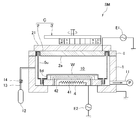
- the sputtering apparatus SM of this embodiment includes a vacuum chamber 1 that defines a processing chamber 10.
- a vacuum pump P is connected to the side wall of the vacuum chamber 1 through an exhaust pipe 11 so that the vacuum chamber 1 can be evacuated to a predetermined pressure (for example, 1 ⁇ 10 ⁇ 5 Pa).
- a gas introduction pipe 13 from a gas source 12 is connected to the side wall of the vacuum chamber 1 so that a rare gas such as argon whose flow rate is controlled by the mass flow controller 14 can be introduced into the vacuum chamber 1.
- the gas source 12, the gas introduction pipe 13 and the mass flow controller 14 constitute the “gas introduction means” of the present invention.
- the cathode unit C is provided at the upper part of the vacuum chamber 1.
- the cathode unit C includes a target 2 and a magnet unit 3 disposed above the target 2.
- the target 2 is made of aluminum oxide and is formed in a circular shape or a rectangular shape in plan view by a known method according to the outline of the substrate W.
- the target 2 is bonded to a copper backing plate 21 that cools the target 2 during film formation via a bonding material (not shown) such as indium or tin.
- a bonding material such as indium or tin.
- the insulating plate I is placed with the sputtering surface 2a of the target 2 facing downward. It is attached to the upper part of the vacuum chamber 1 via.
- the target 2 is connected to the output of a high-frequency power source as the sputtering power source E1, and a high-frequency power of 13.56 MHz, for example, is input to the target 2 during the sputtering from 1 kW to 4 kW.
- the magnet unit 3 has a known structure that generates a magnetic field in the space below the sputter surface 2a, captures electrons etc. ionized below the sputter surface 2a during sputtering, and efficiently ionizes the sputtered particles scattered from the target 2. The detailed description is omitted here.
- a stage 4 that holds the substrate W at a position facing the target 2 is provided at the lower part of the vacuum chamber 1.
- the stage 4 is provided with an electrode for electrostatic chuck (not shown), and the substrate W can be positioned and held by applying a chuck voltage to the electrode.
- the stage 4 incorporates a heating means 41 such as a resistance heater, so that the temperature of the substrate W during film formation can be heated and held within the range of 450 ° C. to 550 ° C.
- a passage 42 for circulating a coolant such as cooling water is formed in the stage 4 so that the substrate W held on the stage 4 can be cooled.
- the vacuum chamber 1 is provided with a pair of upper and lower protective plates 5u, 5d made of metal such as stainless steel, and prevents sputter particles from adhering to the inner wall surface of the vacuum chamber 1 during film formation by sputtering. is doing.
- the sputtering apparatus SM has control means (not shown) provided with a known microcomputer, sequencer, etc., and operates the heating means 41, the sputtering power source E1, the mass flow controller 14, the vacuum pump P, and the like. It is designed to control the whole area.
- control means not shown
- the sputtering apparatus SM has control means (not shown) provided with a known microcomputer, sequencer, etc., and operates the heating means 41, the sputtering power source E1, the mass flow controller 14, the vacuum pump P, and the like. It is designed to control the whole area.
- a film forming method using the sputtering apparatus SM will be described.
- the inside of the vacuum chamber 1 (processing chamber 1a) is evacuated to a predetermined degree of vacuum, the substrate W is transported into the vacuum chamber 1 by a transport robot (not shown), and the substrate W is positioned and held on the stage 4.
- the heating means 41 is operated to heat the substrate W to 450 ° C. to 550 ° C.
- argon gas as a sputtering gas is introduced into the vacuum chamber 1 at a flow rate of 175 to 250 sccm (at this time, the pressure is 1.6 to 2.1 Pa), A plasma atmosphere is formed in the processing chamber 10 by applying high-frequency power to the target 2 from the sputtering power supply E1.
- the target 2 is sputtered, and the sputtered particles generated thereby scatter and adhere to and deposit on the surface of the substrate W to form an amorphous aluminum oxide film.
- the high frequency power input to the target 2 is set in a range of, for example, 13.56 MHz and 1 kW to 4 kW. If it is out of this range, productivity and etching resistance may decrease. In addition, when the pressure in the vacuum chamber during film formation is less than 1.6 Pa, the etching resistance may be reduced. On the other hand, when the pressure exceeds 2.1 Pa, the productivity is deteriorated and the distribution of the film thickness in the substrate is deteriorated. You may be invited.
- the substrate W is heated to 450 ° C. to 550 ° C. during film formation by sputtering, the atoms constituting the formed amorphous aluminum oxide film are aluminum oxide formed at room temperature. Compared to the constituent atoms of the film, it becomes easier to move when annealing is performed. For this reason, the aluminum oxide film can be crystallized even if the temperature of the annealing treatment performed after the film formation using the film formation method of this embodiment is lowered to about 800 ° C.
- the temperature of annealing treatment performed after film formation using the film formation method of this embodiment is set to 800. Even when the temperature is lowered to ⁇ 850 ° C., the aluminum oxide film can be crystallized.
- the substrate W is a silicon wafer having a diameter of 300 mm
- the substrate W is set on the stage 4 in the vacuum chamber 1 on which the aluminum oxide target 2 is assembled, and then the heating means 41 is operated to set the temperature of the substrate W. Heated to 450 ° C.
- argon gas is introduced into the vacuum chamber 1 at a flow rate of 200 sccm (at this time, the pressure in the vacuum chamber 1 is 1.8 Pa).
- a plasma atmosphere was formed in the processing chamber 10 by applying high frequency power of 56 MHz and 4 kW, and an amorphous aluminum oxide film was formed on the surface of the substrate W.
- the substrate W on which the amorphous aluminum oxide film is formed is taken out from the sputtering SM, and is heated to 800 ° C. with respect to the amorphous aluminum oxide film by using a lamp annealing apparatus (“RTA-12000” manufactured by ULVAC-RIKO).
- RTA-12000 lamp annealing apparatus manufactured by ULVAC-RIKO
- An annealing treatment was performed at a temperature, and the aluminum oxide film after the annealing treatment was designated as “Invention 1”.
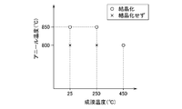
- an amorphous aluminum oxide film was formed by the same method as that of Invention 1 except that the substrate W temperature during film formation was set to 250 ° C. As shown in FIG. 2, it was confirmed that the aluminum oxide film having a film forming temperature of 250 ° C. was not crystallized even when annealed at 800 ° C., and crystallized when annealed at 850 ° C. . Similarly, in the case where the film forming temperature is set to 25 ° C. (room temperature) without operating the heating means 41 during film formation, the film is not crystallized even if the annealing process is performed at 800 ° C. It was confirmed that crystallization occurred when annealing at °C.
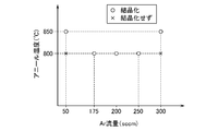
- the argon flow rate was set to 50 sccm, 175 sccm, 200 sccm (the invention 1), 250 sccm, 300 sccm (at this time, the pressure in the vacuum chamber 1 was 0.2 Pa, 1.6 Pa, 1.8 Pa, 2.1 Pa) Except for 2.3 Pa), an amorphous aluminum oxide film was formed by the same method as that of the above-described product 1. As shown in FIG. 3, when the film was formed with the argon flow rate set to 175 sccm, 200 sccm, and 250 sccm, it was confirmed that the film was crystallized by the annealing process at 800 ° C. as in the case of the invention product 1 described above.
- the film was formed with the argon flow rate set to 50 sccm and 300 sccm, it was confirmed that the film was not crystallized by the annealing process at 800 ° C. and crystallized by the annealing process at 850 ° C. From this, it was found that if the argon flow rate is set to 175 to 250 sccm, that is, the pressure in the vacuum chamber 1 during film formation is set to 1.6 to 2.1 Pa, the annealing process can be performed at a low temperature.
- an amorphous aluminum oxide film is formed by the same method as that of the product 1 of the invention, and crystallized by annealing at 800 ° C.
- the crystallized product was designated as Invention Product 2.
- the output of another high-frequency power source E2 is connected to the stage 4, and a predetermined bias power is applied to the stage 4 during film formation, thereby further moving the constituent atoms of the aluminum oxide film during the annealing process. Can be made easier.
Landscapes
- Chemical & Material Sciences (AREA)
- Engineering & Computer Science (AREA)
- Organic Chemistry (AREA)
- Materials Engineering (AREA)
- Mechanical Engineering (AREA)
- Metallurgy (AREA)
- Chemical Kinetics & Catalysis (AREA)
- Physics & Mathematics (AREA)
- Thermal Sciences (AREA)
- Plasma & Fusion (AREA)
- Analytical Chemistry (AREA)
- Physical Vapour Deposition (AREA)
- Optics & Photonics (AREA)
Abstract
Priority Applications (5)
| Application Number | Priority Date | Filing Date | Title |
|---|---|---|---|
| CN201680014796.3A CN107406967B (zh) | 2015-03-10 | 2016-02-16 | 氧化铝膜的成膜方法和形成方法以及溅射装置 |
| SG11201707199PA SG11201707199PA (en) | 2015-03-10 | 2016-02-16 | Method of depositing aluminum oxide film, method of forming the same, and sputtering apparatus |
| US15/555,316 US20180057929A1 (en) | 2015-03-10 | 2016-02-16 | Method of Depositing Aluminum Oxide Film, Method of Forming the Same, and Sputtering Apparatus |
| JP2016524622A JP5978417B1 (ja) | 2015-03-10 | 2016-02-16 | 酸化アルミニウム膜の成膜方法及び形成方法並びにスパッタリング装置 |
| KR1020177027509A KR101871899B1 (ko) | 2015-03-10 | 2016-02-16 | 산화 알루미늄막의 성막 방법 및 형성 방법 및 스퍼터링 장치 |
Applications Claiming Priority (2)
| Application Number | Priority Date | Filing Date | Title |
|---|---|---|---|
| JP2015-046947 | 2015-03-10 | ||
| JP2015046947 | 2015-03-10 |
Publications (1)
| Publication Number | Publication Date |
|---|---|
| WO2016143263A1 true WO2016143263A1 (fr) | 2016-09-15 |
Family
ID=56879422
Family Applications (1)
| Application Number | Title | Priority Date | Filing Date |
|---|---|---|---|
| PCT/JP2016/000786 Ceased WO2016143263A1 (fr) | 2015-03-10 | 2016-02-16 | Procédé de formation et procédé de moulage d'un film d'oxyde d'aluminium, et appareil de pulvérisation |
Country Status (5)
| Country | Link |
|---|---|
| US (1) | US20180057929A1 (fr) |
| KR (1) | KR101871899B1 (fr) |
| CN (1) | CN107406967B (fr) |
| SG (1) | SG11201707199PA (fr) |
| WO (1) | WO2016143263A1 (fr) |
Families Citing this family (2)
| Publication number | Priority date | Publication date | Assignee | Title |
|---|---|---|---|---|
| CN110042365B (zh) * | 2019-03-04 | 2020-09-22 | 中国科学院物理研究所 | 一种在二维材料表面生长氧化铝的原子层沉积方法 |
| KR102697480B1 (ko) * | 2020-09-16 | 2024-08-20 | 가부시키가이샤 알박 | 적층 구조체 및 적층 구조체의 제조 방법 |
Citations (3)
| Publication number | Priority date | Publication date | Assignee | Title |
|---|---|---|---|---|
| JP2000319778A (ja) * | 1999-05-07 | 2000-11-21 | Canon Inc | スパッター装置及びスパッターターゲット |
| JP2013149669A (ja) * | 2012-01-17 | 2013-08-01 | Ulvac Japan Ltd | バリア膜の形成方法、及び強誘電体デバイスの製造方法 |
| JP2014084483A (ja) * | 2012-10-22 | 2014-05-12 | Ulvac Japan Ltd | スパッタリング装置 |
Family Cites Families (4)
| Publication number | Priority date | Publication date | Assignee | Title |
|---|---|---|---|---|
| JP2003168679A (ja) | 2001-12-03 | 2003-06-13 | Nec Kyushu Ltd | 半導体製造装置およびその清掃方法 |
| CN101496117B (zh) * | 2006-07-28 | 2012-04-18 | 株式会社爱发科 | 透明导电膜的成膜方法 |
| JP4965479B2 (ja) * | 2008-02-15 | 2012-07-04 | 株式会社アルバック | スパッタリングターゲットの製造方法及びスパッタリングターゲットの洗浄方法 |
| JP6101533B2 (ja) * | 2013-03-27 | 2017-03-22 | 株式会社Screenホールディングス | 酸化アルミニウムの成膜方法 |
-
2016
- 2016-02-16 SG SG11201707199PA patent/SG11201707199PA/en unknown
- 2016-02-16 US US15/555,316 patent/US20180057929A1/en not_active Abandoned
- 2016-02-16 WO PCT/JP2016/000786 patent/WO2016143263A1/fr not_active Ceased
- 2016-02-16 CN CN201680014796.3A patent/CN107406967B/zh active Active
- 2016-02-16 KR KR1020177027509A patent/KR101871899B1/ko active Active
Patent Citations (3)
| Publication number | Priority date | Publication date | Assignee | Title |
|---|---|---|---|---|
| JP2000319778A (ja) * | 1999-05-07 | 2000-11-21 | Canon Inc | スパッター装置及びスパッターターゲット |
| JP2013149669A (ja) * | 2012-01-17 | 2013-08-01 | Ulvac Japan Ltd | バリア膜の形成方法、及び強誘電体デバイスの製造方法 |
| JP2014084483A (ja) * | 2012-10-22 | 2014-05-12 | Ulvac Japan Ltd | スパッタリング装置 |
Also Published As
| Publication number | Publication date |
|---|---|
| CN107406967A (zh) | 2017-11-28 |
| KR101871899B1 (ko) | 2018-06-27 |
| US20180057929A1 (en) | 2018-03-01 |
| KR20170120175A (ko) | 2017-10-30 |
| SG11201707199PA (en) | 2017-10-30 |
| CN107406967B (zh) | 2019-03-05 |
Similar Documents
| Publication | Publication Date | Title |
|---|---|---|
| TWI723132B (zh) | 利用低溫晶圓溫度之離子束蝕刻 | |
| TWI633579B (zh) | Hard mask forming method and hard mask forming device | |
| EP2942806A1 (fr) | Procédé de gravure | |
| JP4914902B2 (ja) | シリサイド形成方法とその装置 | |
| CN104347521A (zh) | 半导体器件的制造方法 | |
| US9716014B2 (en) | Method of processing workpiece | |
| TWI575327B (zh) | Hard mask manufacturing method | |
| JP5461690B2 (ja) | スパッタリング装置及びスパッタリング方法 | |
| CN102931056B (zh) | 表面处理方法、由碳化硅形成的部件和等离子体处理装置 | |
| JP6140539B2 (ja) | 真空処理装置 | |
| WO2016143263A1 (fr) | Procédé de formation et procédé de moulage d'un film d'oxyde d'aluminium, et appareil de pulvérisation | |
| CN114369804B (zh) | 薄膜沉积方法 | |
| KR102228330B1 (ko) | 에칭 스톱층 및 반도체 디바이스의 제조 방법 | |
| JP5978417B1 (ja) | 酸化アルミニウム膜の成膜方法及び形成方法並びにスパッタリング装置 | |
| KR102361775B1 (ko) | 플라즈마 처리 방법 | |
| TW201409737A (zh) | 太陽電池之製造方法及電漿處理裝置 | |
| JP2017033982A (ja) | 多層膜をエッチングする方法 | |
| TWI571521B (zh) | 於物理蒸汽沉積期間支持工作件的方法 | |
| JP2021066895A (ja) | 成膜方法 | |
| JP4397329B2 (ja) | 薄膜作製装置及び薄膜作製方法 | |
| JP6310678B2 (ja) | スパッタリング方法 | |
| JP6030418B2 (ja) | Pzt膜の形成方法 | |
| JP2016084508A (ja) | 金属膜成膜方法 |
Legal Events
| Date | Code | Title | Description |
|---|---|---|---|
| ENP | Entry into the national phase |
Ref document number: 2016524622 Country of ref document: JP Kind code of ref document: A |
|
| 121 | Ep: the epo has been informed by wipo that ep was designated in this application |
Ref document number: 16761242 Country of ref document: EP Kind code of ref document: A1 |
|
| WWE | Wipo information: entry into national phase |
Ref document number: 15555316 Country of ref document: US |
|
| WWE | Wipo information: entry into national phase |
Ref document number: 11201707199P Country of ref document: SG |
|
| NENP | Non-entry into the national phase |
Ref country code: DE |
|
| ENP | Entry into the national phase |
Ref document number: 20177027509 Country of ref document: KR Kind code of ref document: A |
|
| 122 | Ep: pct application non-entry in european phase |
Ref document number: 16761242 Country of ref document: EP Kind code of ref document: A1 |