WO2016143265A1 - Dispositif à semi-conducteur au nitrure - Google Patents
Dispositif à semi-conducteur au nitrure Download PDFInfo
- Publication number
- WO2016143265A1 WO2016143265A1 PCT/JP2016/000802 JP2016000802W WO2016143265A1 WO 2016143265 A1 WO2016143265 A1 WO 2016143265A1 JP 2016000802 W JP2016000802 W JP 2016000802W WO 2016143265 A1 WO2016143265 A1 WO 2016143265A1
- Authority
- WO
- WIPO (PCT)
- Prior art keywords
- nitride semiconductor
- semiconductor layer
- semiconductor device
- electrode
- disposed
- Prior art date
- Legal status (The legal status is an assumption and is not a legal conclusion. Google has not performed a legal analysis and makes no representation as to the accuracy of the status listed.)
- Ceased
Links
Images


Classifications
-
- H—ELECTRICITY
- H10—SEMICONDUCTOR DEVICES; ELECTRIC SOLID-STATE DEVICES NOT OTHERWISE PROVIDED FOR
- H10D—INORGANIC ELECTRIC SEMICONDUCTOR DEVICES
- H10D30/00—Field-effect transistors [FET]
- H10D30/40—FETs having zero-dimensional [0D], one-dimensional [1D] or two-dimensional [2D] charge carrier gas channels
- H10D30/47—FETs having zero-dimensional [0D], one-dimensional [1D] or two-dimensional [2D] charge carrier gas channels having two-dimensional [2D] charge carrier gas channels, e.g. nanoribbon FETs or high electron mobility transistors [HEMT]
-
- H—ELECTRICITY
- H10—SEMICONDUCTOR DEVICES; ELECTRIC SOLID-STATE DEVICES NOT OTHERWISE PROVIDED FOR
- H10D—INORGANIC ELECTRIC SEMICONDUCTOR DEVICES
- H10D30/00—Field-effect transistors [FET]
- H10D30/80—FETs having rectifying junction gate electrodes
- H10D30/83—FETs having PN junction gate electrodes
-
- H—ELECTRICITY
- H10—SEMICONDUCTOR DEVICES; ELECTRIC SOLID-STATE DEVICES NOT OTHERWISE PROVIDED FOR
- H10D—INORGANIC ELECTRIC SEMICONDUCTOR DEVICES
- H10D30/00—Field-effect transistors [FET]
- H10D30/80—FETs having rectifying junction gate electrodes
- H10D30/87—FETs having Schottky gate electrodes, e.g. metal-semiconductor FETs [MESFET]
-
- H—ELECTRICITY
- H10—SEMICONDUCTOR DEVICES; ELECTRIC SOLID-STATE DEVICES NOT OTHERWISE PROVIDED FOR
- H10H—INORGANIC LIGHT-EMITTING SEMICONDUCTOR DEVICES HAVING POTENTIAL BARRIERS
- H10H20/00—Individual inorganic light-emitting semiconductor devices having potential barriers, e.g. light-emitting diodes [LED]
- H10H20/062—Light-emitting semiconductor devices having field effect type light-emitting regions, e.g. light-emitting High-Electron Mobility Transistors
-
- H—ELECTRICITY
- H10—SEMICONDUCTOR DEVICES; ELECTRIC SOLID-STATE DEVICES NOT OTHERWISE PROVIDED FOR
- H10H—INORGANIC LIGHT-EMITTING SEMICONDUCTOR DEVICES HAVING POTENTIAL BARRIERS
- H10H20/00—Individual inorganic light-emitting semiconductor devices having potential barriers, e.g. light-emitting diodes [LED]
- H10H20/80—Constructional details
- H10H20/81—Bodies
- H10H20/822—Materials of the light-emitting regions
- H10H20/824—Materials of the light-emitting regions comprising only Group III-V materials, e.g. GaP
- H10H20/825—Materials of the light-emitting regions comprising only Group III-V materials, e.g. GaP containing nitrogen, e.g. GaN
-
- H—ELECTRICITY
- H10—SEMICONDUCTOR DEVICES; ELECTRIC SOLID-STATE DEVICES NOT OTHERWISE PROVIDED FOR
- H10D—INORGANIC ELECTRIC SEMICONDUCTOR DEVICES
- H10D48/00—Individual devices not covered by groups H10D1/00 - H10D44/00
- H10D48/30—Devices controlled by electric currents or voltages
- H10D48/32—Devices controlled by only the electric current supplied, or only the electric potential applied, to an electrode which does not carry the current to be rectified, amplified or switched
- H10D48/34—Bipolar devices
- H10D48/345—Bipolar transistors having ohmic electrodes on emitter-like, base-like, and collector-like regions
-
- H—ELECTRICITY
- H10—SEMICONDUCTOR DEVICES; ELECTRIC SOLID-STATE DEVICES NOT OTHERWISE PROVIDED FOR
- H10D—INORGANIC ELECTRIC SEMICONDUCTOR DEVICES
- H10D62/00—Semiconductor bodies, or regions thereof, of devices having potential barriers
- H10D62/10—Shapes, relative sizes or dispositions of the regions of the semiconductor bodies; Shapes of the semiconductor bodies
- H10D62/13—Semiconductor regions connected to electrodes carrying current to be rectified, amplified or switched, e.g. source or drain regions
-
- H—ELECTRICITY
- H10—SEMICONDUCTOR DEVICES; ELECTRIC SOLID-STATE DEVICES NOT OTHERWISE PROVIDED FOR
- H10D—INORGANIC ELECTRIC SEMICONDUCTOR DEVICES
- H10D62/00—Semiconductor bodies, or regions thereof, of devices having potential barriers
- H10D62/10—Shapes, relative sizes or dispositions of the regions of the semiconductor bodies; Shapes of the semiconductor bodies
- H10D62/17—Semiconductor regions connected to electrodes not carrying current to be rectified, amplified or switched, e.g. channel regions
-
- H—ELECTRICITY
- H10—SEMICONDUCTOR DEVICES; ELECTRIC SOLID-STATE DEVICES NOT OTHERWISE PROVIDED FOR
- H10D—INORGANIC ELECTRIC SEMICONDUCTOR DEVICES
- H10D62/00—Semiconductor bodies, or regions thereof, of devices having potential barriers
- H10D62/80—Semiconductor bodies, or regions thereof, of devices having potential barriers characterised by the materials
- H10D62/85—Semiconductor bodies, or regions thereof, of devices having potential barriers characterised by the materials being Group III-V materials, e.g. GaAs
- H10D62/8503—Nitride Group III-V materials, e.g. AlN or GaN
-
- H—ELECTRICITY
- H10—SEMICONDUCTOR DEVICES; ELECTRIC SOLID-STATE DEVICES NOT OTHERWISE PROVIDED FOR
- H10H—INORGANIC LIGHT-EMITTING SEMICONDUCTOR DEVICES HAVING POTENTIAL BARRIERS
- H10H20/00—Individual inorganic light-emitting semiconductor devices having potential barriers, e.g. light-emitting diodes [LED]
- H10H20/80—Constructional details
- H10H20/81—Bodies
- H10H20/819—Bodies characterised by their shape, e.g. curved or truncated substrates
-
- H—ELECTRICITY
- H10—SEMICONDUCTOR DEVICES; ELECTRIC SOLID-STATE DEVICES NOT OTHERWISE PROVIDED FOR
- H10H—INORGANIC LIGHT-EMITTING SEMICONDUCTOR DEVICES HAVING POTENTIAL BARRIERS
- H10H20/00—Individual inorganic light-emitting semiconductor devices having potential barriers, e.g. light-emitting diodes [LED]
- H10H20/80—Constructional details
- H10H20/83—Electrodes
- H10H20/831—Electrodes characterised by their shape
Definitions
- the present disclosure relates to a semiconductor device, particularly a nitride semiconductor device.
- Group III nitride semiconductors are promising as materials for high voltage transistors because they have a larger band gap and dielectric breakdown field than conventional semiconductors such as silicon (Si).
- a group III nitride semiconductor transistor a lateral transistor using a two-dimensional electron gas generated at a heterojunction interface of a group III nitride semiconductor as a channel is generally used.
- the lateral transistor since the lateral transistor has a structure in which the respective electrodes are arranged in a plane on the surface, electric field concentration occurs on the end surface of the drain electrode, and the breakdown voltage tends to decrease.
- the group III nitride semiconductor vertical transistor is required to have a high breakdown voltage and a low on-resistance, and to be normally off from the viewpoint of safety during device operation.
- an n-type GaN layer doped with Si is generally used as a donor.
- the Si doping concentration is increased too much in order to reduce the on-resistance, a large amount of crystal defects are formed, and the breakdown voltage is significantly reduced.
- the vertical transistor is normally on.
- the Si doping concentration is lowered for normally-off or high breakdown voltage, the on-resistance increases. Therefore, it has been very difficult to achieve both normally-off, low on-resistance and high breakdown voltage in the conventional group III nitride semiconductor vertical transistor.
- an object of the present invention is to provide a nitride semiconductor device capable of realizing a group III nitride semiconductor vertical transistor having normally-off, high breakdown voltage, and low on-resistance.
- a nitride semiconductor device is a first conductivity type substrate, which has a first surface and a second surface opposite to the first surface.
- a first nitride semiconductor layer of the first conductivity type disposed on the first surface of the substrate and containing an acceptor impurity; and disposed on the first nitride semiconductor layer; and
- Two electrodes, and a gate electrode disposed on the second nitride semiconductor layer.
- a group III nitride semiconductor vertical transistor having normally-off, high breakdown voltage, and low on-resistance can be realized.
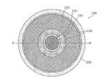
- FIG. 1 is a plan view of the semiconductor device according to the first embodiment.
- FIG. 2 is a cross-sectional view of the semiconductor device according to the first embodiment taken along line A-A ′ of FIG.
- FIG. 3 is a plan view of the semiconductor device according to the first modification of the first embodiment.
- FIG. 4 is a cross-sectional view of the semiconductor device according to Modification 1 of Embodiment 1 taken along line B-B ′ shown in FIG. 3.
- FIG. 5 is a plan view of the semiconductor device according to the second modification of the first embodiment.
- FIG. 6 is a cross-sectional view of the semiconductor device according to Modification 2 of Embodiment 1 taken along the line C-C ′ shown in FIG. 5.
- FIG. 5 is a plan view of the semiconductor device according to the second modification of the first embodiment.
- FIG. 6 is a cross-sectional view of the semiconductor device according to Modification 2 of Embodiment 1 taken along the line C-C ′ shown in FIG. 5.
- FIG. 5 is
- FIG. 7 is a plan view of the semiconductor device according to the third modification of the first embodiment.
- FIG. 8 is a cross-sectional view of the semiconductor device according to the third modification of the first embodiment taken along the line D-D ′ shown in FIG. 7.
- FIG. 9 is a plan view of the semiconductor device according to the fourth modification of the first embodiment.
- FIG. 10 is a cross-sectional view of the semiconductor device according to Modification 4 of Embodiment 1 taken along the line E-E ′ shown in FIG. 9.
- FIG. 11 is a plan view of the semiconductor device according to the second embodiment.
- FIG. 12 is a sectional view of the semiconductor device according to the second embodiment taken along the line F-F ′ of FIG. 11.
- FIG. 13 is a plan view of the semiconductor device according to the third embodiment.
- FIG. 14 is a cross-sectional view of the semiconductor device according to the third embodiment taken along the line G-G ′ of FIG. 13.
- FIG. 15 is a cross-sectional view of a semiconductor device according to a modification of the third embodiment.
- FIG. 16 is a plan view of the semiconductor device according to the fourth embodiment.
- FIG. 17 is a cross-sectional view of the semiconductor device according to the fourth embodiment taken along line H-H ′ of FIG.
- FIG. 18 is a plan view of the semiconductor device according to the first modification of the fourth embodiment.
- FIG. 19 is a cross-sectional view of the semiconductor device according to Modification 1 of Embodiment 4 taken along the line I-I ′ of FIG.
- FIG. 20 is a plan view of a semiconductor device according to the second modification of the fourth embodiment.
- FIG. 20 is a plan view of a semiconductor device according to the second modification of the fourth embodiment.
- FIG. 21 is a cross-sectional view of the semiconductor device according to Modification 2 of Embodiment 4 taken along the line J-J ′ of FIG.
- FIG. 22 is a plan view of a semiconductor device according to the third modification of the fourth embodiment.
- 23 is a cross-sectional view of the semiconductor device according to Modification 3 of Embodiment 4 taken along the line K-K ′ of FIG.
- the first conductivity type is N-type and the second conductivity type is P-type.
- the plan view is hatched corresponding to the cross-sectional view.
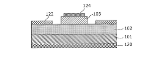
- FIG. 1 is a plan view of a semiconductor device 100 according to the first embodiment.
- FIG. 2 is a sectional view of the semiconductor device 100 according to the first embodiment taken along the line AA ′ in FIG.
- “plan view” means viewing from the normal direction of the main surface of the substrate 101. In order to facilitate understanding of the configuration of the semiconductor device according to the present embodiment, the plan view is given the same pattern as the cross-sectional view.
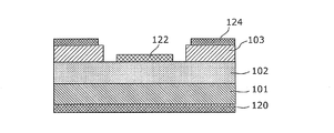
- the semiconductor device 100 includes a substrate 101 having a first surface S1 and a second surface S2 facing the first surface S1, and a first nitridation disposed on the first surface S1 of the substrate 101. And a second nitride semiconductor layer disposed on the first nitride semiconductor layer.
- the substrate 101 and the first nitride semiconductor layer 102 are of the first conductivity type.
- the second nitride semiconductor layer 103 is of the second conductivity type.
- the semiconductor device 100 corresponds to the nitride semiconductor device of the present invention.
- the semiconductor device 100 includes a first electrode 120 disposed on the second surface S2 of the substrate 101, a second electrode 122 disposed on the first nitride semiconductor layer 102, a second And a gate electrode 124 disposed on the nitride semiconductor layer 103.
- the substrate 101 is of the first conductivity type and is made of, for example, GaN.
- the first nitride semiconductor layer 102 is of the first conductivity type, and is made of, for example, In x Al y Ga 1-xy N (0 ⁇ x ⁇ 1, 0 ⁇ y ⁇ 1, 0 ⁇ x + y ⁇ 1). Composed.
- the second nitride semiconductor layer 103 is of the second conductivity type, and is made of, for example, In x Al y Ga 1-xy N (0 ⁇ x ⁇ 1, 0 ⁇ y ⁇ 1, 0 ⁇ x + y ⁇ 1). Composed.
- the first nitride semiconductor layer 102 includes an acceptor impurity.
- An acceptor refers to an atom that supplies holes.
- acceptor atoms implanted into the semiconductor layer are called acceptor impurities.
- carbon or a transition metal can be used as the acceptor impurity.
- the carbon concentration is preferably 1 ⁇ 10 16 / cm 2 to 1 ⁇ 10 19 / cm 2 .
- nitride semiconductor layer 102 when a nitride semiconductor layer is crystal-grown, it becomes n-type naturally due to crystal defects and residual impurities acting as donors.
- the acceptor impurity contained in the first nitride semiconductor layer 102 partially compensates for these donors, whereby the first nitride semiconductor layer 102 becomes highly insulating.
- the Al composition of the first nitride semiconductor layer 102 and the second nitride semiconductor layer 103 (that is, the value of y in In x Al y Ga 1-xy N) is adversely affected by lattice mismatch strain with the substrate 101. It is preferable to increase the height within a range that does not appear. With this configuration, since the band gap of each layer is increased, the breakdown voltage of the semiconductor device is improved.
- the second nitride semiconductor layer 103 includes, for example, magnesium.
- the magnesium concentration of the second nitride semiconductor layer 103 is preferably 5 ⁇ 10 17 / cm 2 to 5 ⁇ 10 20 / cm 2 .
- the substrate 101 is a first conductivity type GaN substrate
- the first nitride semiconductor layer 102 is a first conductivity type GaN layer
- the second nitride semiconductor layer 103 is a second conductivity type. It is assumed that it is a conductive GaN layer.
- the source electrode is an ohmic electrode.
- the drain electrode may be an ohmic electrode or a Schottky electrode.
- the first electrode 120 is referred to as a source electrode 120 and the second electrode 122 is referred to as a drain electrode 122.
- the gate electrode 124 and the drain electrode 122 are arranged side by side (in a direction parallel to the main surface of the substrate), the gate electrode 124 and the drain electrode 122 are arranged so as not to be broken due to electric field concentration on the end surface of the drain electrode 122.
- the distance between the drain electrode 122 is about 20 ⁇ m. Since the highly insulating first nitride semiconductor layer 102 is formed between the source electrode 120 and the drain electrode 122, high breakdown voltage and normally-off are realized.
- the source electrode is an ohmic electrode.
- the drain electrode may be an ohmic electrode or a Schottky electrode.
- the first electrode 120 is referred to as the drain electrode 120 and the second electrode 122 is referred to as the source electrode 122.
- a voltage of 0 V is applied to the gate electrode 124
- a voltage of 0 V is applied to the source electrode 122
- a voltage of +1000 V is applied to the drain electrode 120. Since the highly insulating first nitride semiconductor layer 102 is formed between the source electrode 122 and the drain electrode 120, high breakdown voltage and normally-off are realized.
- a voltage of +3.4 V or higher is applied to the gate electrode 124. Then, holes flow from the second nitride semiconductor layer 103 into the first nitride semiconductor layer 102.
- the first nitride semiconductor layer 102 is highly insulating, there are residual donors that are not completely compensated for by acceptor impurities. Light emission is generated by recombination of electrons and holes generated by the residual donor.
- the current flows through the first insulating semiconductor layer 102 with high insulation and high withstand voltage, which should be essentially free of current by the above process, by light injection accompanying application of the gate voltage.
- a first nitride having a carbon concentration of 3 ⁇ 10 16 / cm 2 and a film thickness of 12 ⁇ m is formed by MOCVD (Metal Organic Chemical Deposition), for example.
- MOCVD Metal Organic Chemical Deposition
- a second nitride semiconductor layer 103 made of, for example, p-type GaN having a magnesium concentration of 1 ⁇ 10 19 / cm 2 and having a thickness of 500 nm is grown on the first nitride semiconductor layer 102 by MOCVD. To do.
- a resist is applied over the second nitride semiconductor layer 103 and patterned. After patterning the resist, the second nitride semiconductor layer 103 is dry etched.
- boron ions are implanted into the first nitride semiconductor layer 102 to form the element isolation portion 202.
- an Al layer having a thickness of 200 nm is disposed on a Ti layer having a thickness of 20 nm.
- Two electrodes 122 are formed.
- the first electrode 120 in which an Al layer having a thickness of 200 nm is disposed on a Ti layer having a thickness of 20 nm is formed.
- a gate electrode 124 is formed in which an Au layer having a thickness of 500 nm is disposed on a Ni layer having a thickness of 100 nm.
- a current flows through the high-insulation and high-breakdown-voltage first nitride semiconductor layer 102 where the current should not substantially flow by light injection accompanying the gate voltage application.
- a group III nitride semiconductor vertical transistor having normally-off, high breakdown voltage, and low on-resistance can be realized.
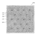
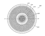
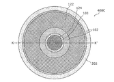
- FIG. 3 is a plan view of the semiconductor device 100a according to the first modification of the first embodiment.
- 4 is a cross-sectional view of the semiconductor device 100a taken along line B-B 'shown in FIG.
- the semiconductor device 100 a has a plurality of circular second nitride semiconductor layers 103 arranged on the first nitride semiconductor layer 102 in plan view.
- a gate electrode 124 is disposed on each of the plurality of second nitride semiconductor layers 103 as shown in FIG.
- a second electrode 122 is disposed between the plurality of second nitride semiconductor layers 103.
- the plurality of gate electrodes 124 may be electrically connected to each other.
- each second nitride semiconductor layer 103 in plan view is not limited to a circular shape, and may be a polygonal shape such as a quadrangle. Further, the arrangement of the plurality of second nitride semiconductor layers 103 is not particularly limited as long as the apparatus operates normally.
- the area occupied by the second electrode 122 in plan view is made larger than the area occupied by the gate electrode 124, that is, between the first electrode 120 and the second electrode 122, that is, Since the channel region between the source electrode and the drain electrode can be widened, the on-resistance can be further suppressed.
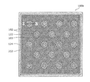
- FIG. 5 is a plan view of the semiconductor device 100b according to the second modification of the first embodiment.
- 6 is a cross-sectional view of the semiconductor device 100b according to the second modification of the first embodiment taken along the line C-C 'shown in FIG.
- the semiconductor device 100 b has a plurality of circular second electrodes 122 arranged on the first nitride semiconductor layer 102 in plan view.
- a second nitride semiconductor layer 103 is disposed between the plurality of second electrodes 122.
- a gate electrode 124 is disposed on each of the plurality of second nitride semiconductor layers 103 as shown in FIG.
- the plurality of second electrodes 122 may be electrically connected to each other.
- each second electrode 122 in plan view is not limited to a circular shape, and may be a polygonal shape such as a quadrangle.
- the arrangement of the plurality of second electrodes 122 is not particularly limited as long as the apparatus operates normally.
- the area occupied by the gate electrode 124 can be made larger than the area occupied by the second electrode 122 in plan view. Therefore, since the concentration of injected holes becomes high, it becomes possible to recombine electrons and holes with higher probability.
- FIG. 7 is a plan view of the semiconductor device 100c according to the third modification of the first embodiment.
- FIG. 8 is a cross-sectional view of the semiconductor device 100c according to the third modification of the first embodiment taken along the line D-D ′ shown in FIG.
- the semiconductor device 100 c includes a plurality of linear second nitride semiconductor layers 103 arranged on the first nitride semiconductor layer 102 in plan view.
- a gate electrode 124 is disposed on each of the plurality of second nitride semiconductor layers 103 as shown in FIG.
- a second electrode 122 is disposed between the plurality of second nitride semiconductor layers 103.
- the plurality of gate electrodes 124 may be electrically connected to each other.
- the area occupied by the second electrode 122 in plan view is made larger than the area occupied by the gate electrode 124, that is, between the first electrode 120 and the second electrode 122, that is, Since the channel region between the source electrode and the drain electrode can be widened, the on-resistance can be further suppressed.
- FIG. 9 is a plan view of the semiconductor device 100d according to the fourth modification of the first embodiment.
- FIG. 10 is a cross-sectional view of the semiconductor device 100d according to the fourth modification of the first embodiment taken along the line E-E 'shown in FIG.
- a plurality of linear second electrodes 122 are arranged on the first nitride semiconductor layer 102 in plan view.
- a second nitride semiconductor layer 103 is disposed between the plurality of second electrodes 122.
- a gate electrode 124 is disposed on each of the plurality of second nitride semiconductor layers 103 as shown in FIG.
- the plurality of second electrodes 122 may be electrically connected to each other.
- the semiconductor device 100d even when the emission intensity under the gate electrode 124 is weakened by making the area occupied by the gate electrode 124 larger than the area occupied by the second electrode 122 in plan view, The light emitting area can be widened. Therefore, in the semiconductor device 100d, since the concentration of injected holes is high, it is possible to flow current more effectively by recombining electrons and holes with higher probability. Note that the case where the emission intensity becomes weak is assumed, for example, when the Al composition of the first nitride semiconductor layer 102 or the second nitride semiconductor layer 103 is increased in order to increase the breakdown voltage.
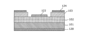
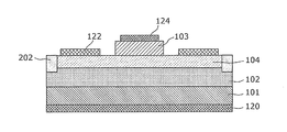
- FIG. 11 is a plan view of the semiconductor device 200 according to the second embodiment.
- FIG. 12 is a cross-sectional view of the semiconductor device 200 according to the second embodiment taken along the line F-F ′ of FIG. 11.
- the semiconductor device 200 according to the second embodiment is arranged between the first nitride semiconductor layer 102 and the second nitride semiconductor layer 103, and as shown in FIG. A third nitride semiconductor layer 104 containing a donor impurity is further provided.
- a material of the third nitride semiconductor layer 104 for example, GaN may be used.
- the silicon concentration may be, for example, 1 ⁇ 10 17 / cm 2 or more.
- the film thickness of the third nitride semiconductor layer 104 may be 100 nm, for example.
- the first electrode 120 may be a drain electrode and the second electrode 122 may be a source electrode. Further, the first electrode 120 may be a source electrode, and the second electrode 122 may be a drain electrode.
- the third nitride semiconductor layer 104 may be formed by MOCVD, for example, after the formation of the first nitride semiconductor layer 102 and before the formation of the second nitride semiconductor layer 103. .
- the semiconductor device 200 according to the second embodiment can emit light with higher efficiency than the semiconductor device 100 according to the first embodiment, the on-resistance is lower than that of the semiconductor device 100 according to the first embodiment. be able to.
- FIG. 13 is a plan view of the semiconductor device 300 according to the third embodiment
- FIG. 14 is a cross-sectional view of the semiconductor device 300 according to the third embodiment taken along the line G-G ′ of FIG.
- the semiconductor device 300 is disposed between the first nitride semiconductor layer 102 and the second nitride semiconductor layer 103 and has a band gap larger than that of the first nitride semiconductor layer 102.
- the fourth nitride semiconductor layer 105 having a large thickness is provided.
- the first nitride semiconductor layer 102 is made of GaN
- Al 0.3 Ga 0.7 N may be used as the material of the fourth nitride semiconductor layer 105.
- the film thickness of Al 0.3 Ga 0.7 N may be about 20 nm, for example.
- the first electrode 120 may be a drain electrode and the second electrode 122 may be a source electrode. Further, the first electrode 120 may be a source electrode, and the second electrode 122 may be a drain electrode.
- the fourth nitride semiconductor layer 105 may be formed by MOCVD.
- a high-density two-dimensional electron gas 126 is formed between the first nitride semiconductor layer 102 and the fourth nitride semiconductor layer 105 by spontaneous polarization and piezoelectric polarization. Therefore, when a voltage is applied to the gate electrode 124, holes are injected into the two-dimensional electron gas 126, whereby high-density electrons and holes can be recombined.
- the semiconductor device 300 according to the third embodiment can emit light with higher efficiency than the semiconductor device 100 according to the first embodiment, the on-resistance can be lowered as compared with the first embodiment.
- the third nitride semiconductor layer 104 described in Embodiment 2 is used between the second nitride semiconductor layer 103 and the fourth nitride semiconductor layer 105 or between the first nitride semiconductor layer 102 and the fourth nitride. It may be disposed anywhere between the physical semiconductor layer 105.
- FIG. 15 is a sectional view of a semiconductor device 300a according to a modification of the third embodiment. Although a plan view of the semiconductor device 300a is omitted, the configuration is substantially the same as that of the semiconductor device 300 shown in FIG.
- the semiconductor device 300 a is provided with a first recess 128 that penetrates the fourth nitride semiconductor layer 105 and reaches at least the first nitride semiconductor layer 102.
- a second electrode 122 is disposed in the first recess 128.
- the second electrode 122 is preferably in contact with the two-dimensional electron gas 126.
- a resist is applied to the fourth nitride semiconductor layer 105 and patterned. After patterning the resist, the fourth recess semiconductor layer 105 and the first nitride semiconductor layer 102 may be dry-etched to form the first recess 128.
- FIG. 16 is a plan view of the semiconductor device 400 according to the fourth embodiment.
- FIG. 17 is a cross-sectional view of the semiconductor device 400 according to the fourth embodiment taken along the line H-H ′ of FIG. 16.
- the semiconductor device 400 is located between the first nitride semiconductor layer 102 and the second nitride semiconductor layer 103 from the first nitride semiconductor layer 102 side.
- a fifth nitride semiconductor layer 106, a sixth nitride semiconductor layer 107, and a seventh nitride semiconductor layer 108 are stacked in this order.
- the band gap of the fifth nitride semiconductor layer 106 is greater than or equal to the band gap of the first nitride semiconductor layer 102.
- the band gap of the sixth nitride semiconductor layer 107 is smaller than the band gap of the fifth nitride semiconductor layer 106.
- the band gap of the seventh nitride semiconductor layer 108 is greater than or equal to the band gap of the first nitride semiconductor layer 102 and larger than the band gap of the sixth nitride semiconductor layer 106. Note that the fifth nitride semiconductor layer 106 and the seventh nitride semiconductor layer 108 may be made of the same material.
- the first electrode 120 may be a drain electrode and the second electrode 122 may be a source electrode. Further, the first electrode 120 may be a source electrode, and the second electrode 122 may be a drain electrode.
- quantum levels are formed in the sixth nitride semiconductor layer 107 by the electron and hole confinement effect of the fifth nitride semiconductor layer 106 and the seventh nitride semiconductor layer 108.
- the probability of recombination of electrons and holes is improved.
- the semiconductor device 400 according to the fourth embodiment can emit light with higher efficiency than the semiconductor device 100 according to the first embodiment, the on-resistance is lower than that of the semiconductor device 100 according to the first embodiment. be able to.
- the fifth nitride semiconductor layer 106, the sixth nitride semiconductor layer 107, and the seventh nitride semiconductor layer 108 may have a multiple quantum well (MQW) structure formed sequentially and repeatedly. It is desirable that there are three layers of the sixth nitride semiconductor layer 107 in which a period, that is, a quantum level is formed.
- MQW multiple quantum well
- the fifth nitride semiconductor layer 106 and the seventh nitride semiconductor layer 108 are made of, for example, Al 0.1 Ga 0.9 N having a thickness of 10 nm.
- the sixth nitride semiconductor layer 107 is made of, for example, GaN having a thickness of 3 nm.
- the fifth nitride semiconductor layer 106 and the sixth nitride semiconductor are formed by MOCVD.
- the layer 107 and the seventh nitride semiconductor layer 108 may be formed sequentially.
- a resist is applied over the second nitride semiconductor layer 103 and patterned.
- the second nitride semiconductor layer 103, the fifth nitride semiconductor layer 106, the sixth nitride semiconductor layer 107, and the seventh nitride semiconductor layer 108 are dry-etched to thereby form the first nitride semiconductor layer 102. To expose.
- the semiconductor device 400 according to the fourth embodiment can emit light with high efficiency, the on-resistance can be lowered as compared with the semiconductor device 100 according to the first embodiment.
- FIG. 18 is a plan view of a semiconductor device 400a according to the first modification of the fourth embodiment.
- FIG. 19 is a cross-sectional view of the semiconductor device 400 according to Modification 1 of Embodiment 4 taken along the line I-I ′ of FIG.
- the second electrode 122 is formed in the second recess 129 formed in the first nitride semiconductor layer 102, and the fifth The nitride semiconductor layer 106, the sixth nitride semiconductor layer 107, and the seventh nitride semiconductor layer 108 are in contact with the side surfaces.
- a two-dimensional electron gas (not shown) formed at the interface between the fifth nitride semiconductor layer 106 and the first nitride semiconductor layer 102 and the second electrode 122 come into contact with each other, whereby the first nitride semiconductor layer 102 is contacted.
- the contact resistance between the first electrode 122 and the second electrode 122 can be reduced. Thereby, the on-resistance of the semiconductor device 400a can be further reduced.
- FIG. 20 is a plan view of the semiconductor device 400b according to the second modification of the fourth embodiment.
- FIG. 21 is a cross-sectional view of the semiconductor device 400b according to Modification 2 of Embodiment 4 taken along the line J-J 'of FIG.
- third nitridation including a donor impurity such as silicon is provided between the first nitride semiconductor layer 102 and the fifth nitride semiconductor layer 106.
- a physical semiconductor layer 104 may be formed.
- FIG. 22 is a plan view of a semiconductor device 400c according to the third modification of the fourth embodiment.
- FIG. 23 is a cross-sectional view of the semiconductor device 400c according to Modification 3 of Embodiment 4 taken along the line K-K ′ of FIG.
- the difference between the semiconductor device 400c according to the present modification and the semiconductor device 400b according to the second modification is that, as shown in FIGS. 22 and 23, the side surface of the third nitride semiconductor layer 104 is the fifth nitride semiconductor layer 106.
- the sixth nitride semiconductor layer 107, the seventh nitride semiconductor layer 108, and the second nitride semiconductor layer 103 are formed on substantially the same plane.
- substantially the same means that a manufacturing error is included.
- the semiconductor device 400c has a shorter distance between the source electrode and the drain electrode than the semiconductor device 400b according to the second modification, and the third nitride semiconductor layer 104 to the sixth nitride semiconductor layer 107. Higher density electrons can flow. As a result, the probability that electrons and holes are recombined in the quantum level of the sixth nitride semiconductor layer 107 is further improved. Therefore, the semiconductor device 400c can further reduce the on-resistance by emitting light with higher efficiency.
- the first conductivity type is the N type and the second conductivity type is the P type, but the first conductivity type is the P type and the second conductivity type is the N type. It is good.
- each nitride semiconductor layer in plan view is not limited to a circular shape, and may be a polygonal shape such as a quadrangle.
- the arrangement of the plurality of nitride semiconductor layers is not particularly limited as long as the device operates normally.
- the nitride semiconductor device according to the present invention can be used as a high-output, high-breakdown-voltage transistor used in a power supply circuit for consumer equipment.
Landscapes
- Junction Field-Effect Transistors (AREA)
Abstract
L'invention concerne un dispositif à semi-conducteur au nitrure (100) qui est pourvu : d'un substrat (101), qui est un substrat d'un premier type de conductivité, et qui a une première surface (S1) et une seconde surface (S2) sur le côté inverse de la première surface (S1) ; d'une première couche semi-conductrice de nitrure (102) du premier type de conductivité, qui est disposée sur la première surface (S1) du substrat (101), et qui contient une impureté d'accepteur ; d'une seconde couche semi-conductrice de nitrure (103) d'un second type de conductivité, qui est disposée sur la première couche semi-conductrice de nitrure (102), et qui est d'un type de conductivité opposé au premier type de conductivité ; d'une première électrode (120) disposée sur la seconde surface (S2) du substrat (101) ; d'une seconde électrode (122) disposée sur la première couche semi-conductrice de nitrure (102) ; et d'une électrode de grille (124) disposée sur la seconde couche semi-conductrice de nitrure (103).
Priority Applications (2)
| Application Number | Priority Date | Filing Date | Title |
|---|---|---|---|
| JP2017504595A JP6685278B2 (ja) | 2015-03-11 | 2016-02-17 | 窒化物半導体装置 |
| US15/695,904 US10249748B2 (en) | 2015-03-11 | 2017-09-05 | Nitride semiconductor device |
Applications Claiming Priority (2)
| Application Number | Priority Date | Filing Date | Title |
|---|---|---|---|
| JP2015-048694 | 2015-03-11 | ||
| JP2015048694 | 2015-03-11 |
Related Child Applications (1)
| Application Number | Title | Priority Date | Filing Date |
|---|---|---|---|
| US15/695,904 Continuation US10249748B2 (en) | 2015-03-11 | 2017-09-05 | Nitride semiconductor device |
Publications (1)
| Publication Number | Publication Date |
|---|---|
| WO2016143265A1 true WO2016143265A1 (fr) | 2016-09-15 |
Family
ID=56880197
Family Applications (1)
| Application Number | Title | Priority Date | Filing Date |
|---|---|---|---|
| PCT/JP2016/000802 Ceased WO2016143265A1 (fr) | 2015-03-11 | 2016-02-17 | Dispositif à semi-conducteur au nitrure |
Country Status (3)
| Country | Link |
|---|---|
| US (1) | US10249748B2 (fr) |
| JP (1) | JP6685278B2 (fr) |
| WO (1) | WO2016143265A1 (fr) |
Families Citing this family (3)
| Publication number | Priority date | Publication date | Assignee | Title |
|---|---|---|---|---|
| DE102020001840B3 (de) | 2020-03-20 | 2021-09-23 | Azur Space Solar Power Gmbh | Stapelförmiges photonisches III-V-Halbleiterbauelement |
| DE102020001837B3 (de) | 2020-03-20 | 2021-08-26 | Azur Space Solar Power Gmbh | Stapelförmiges photonisches lll-V-Halbleiterbauelement |
| US20220376041A1 (en) * | 2021-04-12 | 2022-11-24 | Innoscience (Suzhou) Technology Co., Ltd. | Semiconductor device and method for manufacturing the same |
Citations (4)
| Publication number | Priority date | Publication date | Assignee | Title |
|---|---|---|---|---|
| JP2004006723A (ja) * | 2002-03-25 | 2004-01-08 | Toshiba Corp | 高耐圧半導体装置及びその製造方法 |
| JP2006186336A (ja) * | 2004-11-30 | 2006-07-13 | Matsushita Electric Ind Co Ltd | 電界効果トランジスタ及びその製造方法 |
| JP2010165896A (ja) * | 2009-01-16 | 2010-07-29 | Nec Corp | 半導体装置及びその製造方法 |
| JP2010267881A (ja) * | 2009-05-15 | 2010-11-25 | Panasonic Corp | 電界効果トランジスタ及びその製造方法 |
Family Cites Families (35)
| Publication number | Priority date | Publication date | Assignee | Title |
|---|---|---|---|---|
| US6855970B2 (en) | 2002-03-25 | 2005-02-15 | Kabushiki Kaisha Toshiba | High-breakdown-voltage semiconductor device |
| US7465997B2 (en) * | 2004-02-12 | 2008-12-16 | International Rectifier Corporation | III-nitride bidirectional switch |
| JP4744109B2 (ja) * | 2004-07-20 | 2011-08-10 | トヨタ自動車株式会社 | 半導体装置とその製造方法 |
| US7439595B2 (en) | 2004-11-30 | 2008-10-21 | Matsushita Electric Industrial Co., Ltd. | Field effect transistor having vertical channel structure |
| JP4792814B2 (ja) * | 2005-05-26 | 2011-10-12 | 住友電気工業株式会社 | 高電子移動度トランジスタ、電界効果トランジスタ、エピタキシャル基板、エピタキシャル基板を作製する方法およびiii族窒化物系トランジスタを作製する方法 |
| US8026568B2 (en) * | 2005-11-15 | 2011-09-27 | Velox Semiconductor Corporation | Second Schottky contact metal layer to improve GaN Schottky diode performance |
| JP2007142243A (ja) | 2005-11-21 | 2007-06-07 | Matsushita Electric Ind Co Ltd | 窒化物半導体電界効果トランジスタ及びその製造方法 |
| KR20070117238A (ko) | 2006-06-08 | 2007-12-12 | 삼성전기주식회사 | 반도체 발광 트랜지스터 |
| CN101523614B (zh) * | 2006-11-20 | 2011-04-20 | 松下电器产业株式会社 | 半导体装置及其驱动方法 |
| JP5300238B2 (ja) * | 2006-12-19 | 2013-09-25 | パナソニック株式会社 | 窒化物半導体装置 |
| US20110037101A1 (en) * | 2008-06-05 | 2011-02-17 | Kazushi Nakazawa | Semiconductor device |
| JP2010135640A (ja) * | 2008-12-05 | 2010-06-17 | Panasonic Corp | 電界効果トランジスタ |
| WO2011024367A1 (fr) * | 2009-08-27 | 2011-03-03 | パナソニック株式会社 | Dispositif semi-conducteur au nitrure |
| JP5742072B2 (ja) * | 2010-10-06 | 2015-07-01 | 住友電気工業株式会社 | 半導体装置およびその製造方法 |
| CN105977209B (zh) * | 2010-10-20 | 2019-03-19 | 富士通株式会社 | 半导体装置及其制造方法 |
| JP6132242B2 (ja) * | 2011-07-12 | 2017-05-24 | パナソニックIpマネジメント株式会社 | 窒化物半導体装置およびその製造方法 |
| JP5667588B2 (ja) | 2012-02-15 | 2015-02-12 | 日本電信電話株式会社 | 窒化物半導体発光トランジスタ |
| JP6082229B2 (ja) * | 2012-10-30 | 2017-02-15 | 住友化学株式会社 | 窒化物半導体素子およびその製造方法 |
| JP6170300B2 (ja) * | 2013-01-08 | 2017-07-26 | 住友化学株式会社 | 窒化物半導体デバイス |
| WO2014108946A1 (fr) * | 2013-01-10 | 2014-07-17 | パナソニック株式会社 | Transistor à effet de champ |
| JP6251071B2 (ja) * | 2014-02-05 | 2017-12-20 | ルネサスエレクトロニクス株式会社 | 半導体装置 |
| JP6175009B2 (ja) * | 2014-02-06 | 2017-08-02 | 住友化学株式会社 | 高耐圧窒化ガリウム系半導体デバイス及びその製造方法 |
| JP6511645B2 (ja) * | 2014-02-13 | 2019-05-15 | パナソニックIpマネジメント株式会社 | 窒化物半導体デバイス |
| WO2015125471A1 (fr) * | 2014-02-21 | 2015-08-27 | パナソニック株式会社 | Transistor à effet de champ |
| JP5983684B2 (ja) * | 2014-07-02 | 2016-09-06 | ウシオ電機株式会社 | Led素子 |
| JP6055799B2 (ja) * | 2014-07-29 | 2016-12-27 | 株式会社豊田中央研究所 | 半導体装置とその製造方法 |
| US9590087B2 (en) * | 2014-11-13 | 2017-03-07 | Infineon Technologies Austria Ag | Compound gated semiconductor device having semiconductor field plate |
| JP2016100471A (ja) * | 2014-11-21 | 2016-05-30 | 住友電気工業株式会社 | 半導体装置及び半導体装置の製造方法 |
| JP6319151B2 (ja) * | 2015-03-23 | 2018-05-09 | 豊田合成株式会社 | 半導体装置および半導体装置の製造方法 |
| JP6477396B2 (ja) * | 2015-09-30 | 2019-03-06 | 豊田合成株式会社 | 窒化物半導体装置の製造方法 |
| JP6767741B2 (ja) * | 2015-10-08 | 2020-10-14 | ローム株式会社 | 窒化物半導体装置およびその製造方法 |
| JP2017157711A (ja) * | 2016-03-02 | 2017-09-07 | 株式会社東芝 | 半導体装置 |
| US9954092B2 (en) * | 2016-07-22 | 2018-04-24 | Kabushiki Kaisha Toshiba | Semiconductor device, power circuit, and computer |
| JP6677598B2 (ja) * | 2016-07-25 | 2020-04-08 | ルネサスエレクトロニクス株式会社 | 半導体装置 |
| JP6760556B2 (ja) * | 2016-11-30 | 2020-09-23 | 住友電工デバイス・イノベーション株式会社 | 半導体基板の製造方法 |
-
2016
- 2016-02-17 WO PCT/JP2016/000802 patent/WO2016143265A1/fr not_active Ceased
- 2016-02-17 JP JP2017504595A patent/JP6685278B2/ja active Active
-
2017
- 2017-09-05 US US15/695,904 patent/US10249748B2/en active Active
Patent Citations (4)
| Publication number | Priority date | Publication date | Assignee | Title |
|---|---|---|---|---|
| JP2004006723A (ja) * | 2002-03-25 | 2004-01-08 | Toshiba Corp | 高耐圧半導体装置及びその製造方法 |
| JP2006186336A (ja) * | 2004-11-30 | 2006-07-13 | Matsushita Electric Ind Co Ltd | 電界効果トランジスタ及びその製造方法 |
| JP2010165896A (ja) * | 2009-01-16 | 2010-07-29 | Nec Corp | 半導体装置及びその製造方法 |
| JP2010267881A (ja) * | 2009-05-15 | 2010-11-25 | Panasonic Corp | 電界効果トランジスタ及びその製造方法 |
Also Published As
| Publication number | Publication date |
|---|---|
| US20170365698A1 (en) | 2017-12-21 |
| JP6685278B2 (ja) | 2020-04-22 |
| JPWO2016143265A1 (ja) | 2017-12-21 |
| US10249748B2 (en) | 2019-04-02 |
Similar Documents
| Publication | Publication Date | Title |
|---|---|---|
| JP6371986B2 (ja) | 窒化物半導体構造物 | |
| JP4775859B2 (ja) | 窒化物半導体装置とそれを含む電力変換装置 | |
| JP5654512B2 (ja) | 窒化物半導体装置 | |
| JP5841417B2 (ja) | 窒化物半導体ダイオード | |
| JP5140347B2 (ja) | バイポーラトランジスタ及びその製造方法 | |
| US8350297B2 (en) | Compound semiconductor device and production method thereof | |
| JP6834546B2 (ja) | 半導体装置及びその製造方法 | |
| JPWO2017138505A1 (ja) | 半導体装置 | |
| JP2012231019A (ja) | 炭化珪素ダイオード | |
| WO2012160875A1 (fr) | Elément de commutation | |
| JP5341345B2 (ja) | 窒化物半導体ヘテロ構造電界効果トランジスタ | |
| JP6685278B2 (ja) | 窒化物半導体装置 | |
| JP5689712B2 (ja) | 半導体装置およびその製造方法 | |
| JP4929882B2 (ja) | 半導体装置 | |
| US20080175293A1 (en) | Semiconductor laser device | |
| KR102131697B1 (ko) | 정전기 방전 특성이 향상된 반도체 소자 및 그 제조 방법 | |
| JP2015115433A (ja) | Iii族窒化物半導体素子 | |
| JP2017050511A (ja) | 半導体装置 | |
| JP2013207082A (ja) | 窒化物半導体ショットキダイオードおよびその製造方法 | |
| JP2019057589A (ja) | ダイオード | |
| JP2012094889A (ja) | 半導体装置 | |
| KR101140659B1 (ko) | 화합물 반도체 발광소자 | |
| KR101238878B1 (ko) | 고효율 무분극 질화갈륨계 발광 소자 및 그 제조 방법 | |
| WO2019003363A1 (fr) | Dispositif à semi-conducteur et son procédé de production | |
| US8916885B2 (en) | Semiconductor device with efficient carrier recombination |
Legal Events
| Date | Code | Title | Description |
|---|---|---|---|
| 121 | Ep: the epo has been informed by wipo that ep was designated in this application |
Ref document number: 16761244 Country of ref document: EP Kind code of ref document: A1 |
|
| ENP | Entry into the national phase |
Ref document number: 2017504595 Country of ref document: JP Kind code of ref document: A |
|
| NENP | Non-entry into the national phase |
Ref country code: DE |
|
| 122 | Ep: pct application non-entry in european phase |
Ref document number: 16761244 Country of ref document: EP Kind code of ref document: A1 |