WO2016147264A1 - Dispositif à semi-conducteurs et procédé de fabrication de celui-ci - Google Patents
Dispositif à semi-conducteurs et procédé de fabrication de celui-ci Download PDFInfo
- Publication number
- WO2016147264A1 WO2016147264A1 PCT/JP2015/057539 JP2015057539W WO2016147264A1 WO 2016147264 A1 WO2016147264 A1 WO 2016147264A1 JP 2015057539 W JP2015057539 W JP 2015057539W WO 2016147264 A1 WO2016147264 A1 WO 2016147264A1
- Authority
- WO
- WIPO (PCT)
- Prior art keywords
- proton
- semiconductor device
- phosphorus
- manufacturing
- type buffer
- Prior art date
- Legal status (The legal status is an assumption and is not a legal conclusion. Google has not performed a legal analysis and makes no representation as to the accuracy of the status listed.)
- Ceased
Links
Images


Classifications
-
- H—ELECTRICITY
- H10—SEMICONDUCTOR DEVICES; ELECTRIC SOLID-STATE DEVICES NOT OTHERWISE PROVIDED FOR
- H10P—GENERIC PROCESSES OR APPARATUS FOR THE MANUFACTURE OR TREATMENT OF DEVICES COVERED BY CLASS H10
- H10P30/00—Ion implantation into wafers, substrates or parts of devices
- H10P30/20—Ion implantation into wafers, substrates or parts of devices into semiconductor materials, e.g. for doping
- H10P30/21—Ion implantation into wafers, substrates or parts of devices into semiconductor materials, e.g. for doping of electrically active species
-
- H—ELECTRICITY
- H10—SEMICONDUCTOR DEVICES; ELECTRIC SOLID-STATE DEVICES NOT OTHERWISE PROVIDED FOR
- H10D—INORGANIC ELECTRIC SEMICONDUCTOR DEVICES
- H10D12/00—Bipolar devices controlled by the field effect, e.g. insulated-gate bipolar transistors [IGBT]
-
- H—ELECTRICITY
- H10—SEMICONDUCTOR DEVICES; ELECTRIC SOLID-STATE DEVICES NOT OTHERWISE PROVIDED FOR
- H10D—INORGANIC ELECTRIC SEMICONDUCTOR DEVICES
- H10D12/00—Bipolar devices controlled by the field effect, e.g. insulated-gate bipolar transistors [IGBT]
- H10D12/01—Manufacture or treatment
- H10D12/031—Manufacture or treatment of IGBTs
- H10D12/032—Manufacture or treatment of IGBTs of vertical IGBTs
- H10D12/038—Manufacture or treatment of IGBTs of vertical IGBTs having a recessed gate, e.g. trench-gate IGBTs
-
- H—ELECTRICITY
- H10—SEMICONDUCTOR DEVICES; ELECTRIC SOLID-STATE DEVICES NOT OTHERWISE PROVIDED FOR
- H10D—INORGANIC ELECTRIC SEMICONDUCTOR DEVICES
- H10D12/00—Bipolar devices controlled by the field effect, e.g. insulated-gate bipolar transistors [IGBT]
- H10D12/411—Insulated-gate bipolar transistors [IGBT]
- H10D12/441—Vertical IGBTs
- H10D12/461—Vertical IGBTs having non-planar surfaces, e.g. having trenches, recesses or pillars in the surfaces of the emitter, base or collector regions
- H10D12/481—Vertical IGBTs having non-planar surfaces, e.g. having trenches, recesses or pillars in the surfaces of the emitter, base or collector regions having gate structures on slanted surfaces, on vertical surfaces, or in grooves, e.g. trench gate IGBTs
-
- H—ELECTRICITY
- H10—SEMICONDUCTOR DEVICES; ELECTRIC SOLID-STATE DEVICES NOT OTHERWISE PROVIDED FOR
- H10D—INORGANIC ELECTRIC SEMICONDUCTOR DEVICES
- H10D30/00—Field-effect transistors [FET]
- H10D30/60—Insulated-gate field-effect transistors [IGFET]
-
- H—ELECTRICITY
- H10—SEMICONDUCTOR DEVICES; ELECTRIC SOLID-STATE DEVICES NOT OTHERWISE PROVIDED FOR
- H10D—INORGANIC ELECTRIC SEMICONDUCTOR DEVICES
- H10D62/00—Semiconductor bodies, or regions thereof, of devices having potential barriers
- H10D62/10—Shapes, relative sizes or dispositions of the regions of the semiconductor bodies; Shapes of the semiconductor bodies
- H10D62/13—Semiconductor regions connected to electrodes carrying current to be rectified, amplified or switched, e.g. source or drain regions
- H10D62/133—Emitter regions of BJTs
-
- H—ELECTRICITY
- H10—SEMICONDUCTOR DEVICES; ELECTRIC SOLID-STATE DEVICES NOT OTHERWISE PROVIDED FOR
- H10D—INORGANIC ELECTRIC SEMICONDUCTOR DEVICES
- H10D62/00—Semiconductor bodies, or regions thereof, of devices having potential barriers
- H10D62/10—Shapes, relative sizes or dispositions of the regions of the semiconductor bodies; Shapes of the semiconductor bodies
- H10D62/13—Semiconductor regions connected to electrodes carrying current to be rectified, amplified or switched, e.g. source or drain regions
- H10D62/137—Collector regions of BJTs
-
- H—ELECTRICITY
- H10—SEMICONDUCTOR DEVICES; ELECTRIC SOLID-STATE DEVICES NOT OTHERWISE PROVIDED FOR
- H10D—INORGANIC ELECTRIC SEMICONDUCTOR DEVICES
- H10D62/00—Semiconductor bodies, or regions thereof, of devices having potential barriers
- H10D62/10—Shapes, relative sizes or dispositions of the regions of the semiconductor bodies; Shapes of the semiconductor bodies
- H10D62/17—Semiconductor regions connected to electrodes not carrying current to be rectified, amplified or switched, e.g. channel regions
- H10D62/177—Base regions of bipolar transistors, e.g. BJTs or IGBTs
-
- H—ELECTRICITY
- H10—SEMICONDUCTOR DEVICES; ELECTRIC SOLID-STATE DEVICES NOT OTHERWISE PROVIDED FOR
- H10D—INORGANIC ELECTRIC SEMICONDUCTOR DEVICES
- H10D62/00—Semiconductor bodies, or regions thereof, of devices having potential barriers
- H10D62/50—Physical imperfections
- H10D62/53—Physical imperfections the imperfections being within the semiconductor body
-
- H—ELECTRICITY
- H10—SEMICONDUCTOR DEVICES; ELECTRIC SOLID-STATE DEVICES NOT OTHERWISE PROVIDED FOR
- H10D—INORGANIC ELECTRIC SEMICONDUCTOR DEVICES
- H10D62/00—Semiconductor bodies, or regions thereof, of devices having potential barriers
- H10D62/60—Impurity distributions or concentrations
-
- H—ELECTRICITY
- H10—SEMICONDUCTOR DEVICES; ELECTRIC SOLID-STATE DEVICES NOT OTHERWISE PROVIDED FOR
- H10D—INORGANIC ELECTRIC SEMICONDUCTOR DEVICES
- H10D62/00—Semiconductor bodies, or regions thereof, of devices having potential barriers
- H10D62/80—Semiconductor bodies, or regions thereof, of devices having potential barriers characterised by the materials
- H10D62/83—Semiconductor bodies, or regions thereof, of devices having potential barriers characterised by the materials being Group IV materials, e.g. B-doped Si or undoped Ge
- H10D62/834—Semiconductor bodies, or regions thereof, of devices having potential barriers characterised by the materials being Group IV materials, e.g. B-doped Si or undoped Ge further characterised by the dopants
-
- H—ELECTRICITY
- H10—SEMICONDUCTOR DEVICES; ELECTRIC SOLID-STATE DEVICES NOT OTHERWISE PROVIDED FOR
- H10D—INORGANIC ELECTRIC SEMICONDUCTOR DEVICES
- H10D64/00—Electrodes of devices having potential barriers
- H10D64/20—Electrodes characterised by their shapes, relative sizes or dispositions
- H10D64/23—Electrodes carrying the current to be rectified, amplified, oscillated or switched, e.g. sources, drains, anodes or cathodes
- H10D64/231—Emitter or collector electrodes for bipolar transistors
-
- H—ELECTRICITY
- H10—SEMICONDUCTOR DEVICES; ELECTRIC SOLID-STATE DEVICES NOT OTHERWISE PROVIDED FOR
- H10D—INORGANIC ELECTRIC SEMICONDUCTOR DEVICES
- H10D8/00—Diodes
-
- H—ELECTRICITY
- H10—SEMICONDUCTOR DEVICES; ELECTRIC SOLID-STATE DEVICES NOT OTHERWISE PROVIDED FOR
- H10D—INORGANIC ELECTRIC SEMICONDUCTOR DEVICES
- H10D8/00—Diodes
- H10D8/01—Manufacture or treatment
- H10D8/045—Manufacture or treatment of PN junction diodes
-
- H—ELECTRICITY
- H10—SEMICONDUCTOR DEVICES; ELECTRIC SOLID-STATE DEVICES NOT OTHERWISE PROVIDED FOR
- H10P—GENERIC PROCESSES OR APPARATUS FOR THE MANUFACTURE OR TREATMENT OF DEVICES COVERED BY CLASS H10
- H10P14/00—Formation of materials, e.g. in the shape of layers or pillars
- H10P14/40—Formation of materials, e.g. in the shape of layers or pillars of conductive or resistive materials
-
- H—ELECTRICITY
- H10—SEMICONDUCTOR DEVICES; ELECTRIC SOLID-STATE DEVICES NOT OTHERWISE PROVIDED FOR
- H10P—GENERIC PROCESSES OR APPARATUS FOR THE MANUFACTURE OR TREATMENT OF DEVICES COVERED BY CLASS H10
- H10P30/00—Ion implantation into wafers, substrates or parts of devices
- H10P30/20—Ion implantation into wafers, substrates or parts of devices into semiconductor materials, e.g. for doping
- H10P30/202—Ion implantation into wafers, substrates or parts of devices into semiconductor materials, e.g. for doping characterised by the semiconductor materials
- H10P30/204—Ion implantation into wafers, substrates or parts of devices into semiconductor materials, e.g. for doping characterised by the semiconductor materials into Group IV semiconductors
-
- H—ELECTRICITY
- H10—SEMICONDUCTOR DEVICES; ELECTRIC SOLID-STATE DEVICES NOT OTHERWISE PROVIDED FOR
- H10P—GENERIC PROCESSES OR APPARATUS FOR THE MANUFACTURE OR TREATMENT OF DEVICES COVERED BY CLASS H10
- H10P30/00—Ion implantation into wafers, substrates or parts of devices
- H10P30/20—Ion implantation into wafers, substrates or parts of devices into semiconductor materials, e.g. for doping
- H10P30/208—Ion implantation into wafers, substrates or parts of devices into semiconductor materials, e.g. for doping of electrically inactive species
-
- H—ELECTRICITY
- H10—SEMICONDUCTOR DEVICES; ELECTRIC SOLID-STATE DEVICES NOT OTHERWISE PROVIDED FOR
- H10P—GENERIC PROCESSES OR APPARATUS FOR THE MANUFACTURE OR TREATMENT OF DEVICES COVERED BY CLASS H10
- H10P30/00—Ion implantation into wafers, substrates or parts of devices
- H10P30/20—Ion implantation into wafers, substrates or parts of devices into semiconductor materials, e.g. for doping
- H10P30/28—Ion implantation into wafers, substrates or parts of devices into semiconductor materials, e.g. for doping characterised by an annealing step, e.g. for activation of dopants
-
- H—ELECTRICITY
- H10—SEMICONDUCTOR DEVICES; ELECTRIC SOLID-STATE DEVICES NOT OTHERWISE PROVIDED FOR
- H10P—GENERIC PROCESSES OR APPARATUS FOR THE MANUFACTURE OR TREATMENT OF DEVICES COVERED BY CLASS H10
- H10P34/00—Irradiation with electromagnetic or particle radiation of wafers, substrates or parts of devices
- H10P34/40—Irradiation with electromagnetic or particle radiation of wafers, substrates or parts of devices with high-energy radiation
- H10P34/42—Irradiation with electromagnetic or particle radiation of wafers, substrates or parts of devices with high-energy radiation with electromagnetic radiation, e.g. laser annealing
-
- H—ELECTRICITY
- H10—SEMICONDUCTOR DEVICES; ELECTRIC SOLID-STATE DEVICES NOT OTHERWISE PROVIDED FOR
- H10P—GENERIC PROCESSES OR APPARATUS FOR THE MANUFACTURE OR TREATMENT OF DEVICES COVERED BY CLASS H10
- H10P95/00—Generic processes or apparatus for manufacture or treatments not covered by the other groups of this subclass
- H10P95/90—Thermal treatments, e.g. annealing or sintering
-
- H—ELECTRICITY
- H10—SEMICONDUCTOR DEVICES; ELECTRIC SOLID-STATE DEVICES NOT OTHERWISE PROVIDED FOR
- H10D—INORGANIC ELECTRIC SEMICONDUCTOR DEVICES
- H10D62/00—Semiconductor bodies, or regions thereof, of devices having potential barriers
- H10D62/10—Shapes, relative sizes or dispositions of the regions of the semiconductor bodies; Shapes of the semiconductor bodies
- H10D62/124—Shapes, relative sizes or dispositions of the regions of semiconductor bodies or of junctions between the regions
- H10D62/126—Top-view geometrical layouts of the regions or the junctions
- H10D62/127—Top-view geometrical layouts of the regions or the junctions of cellular field-effect devices, e.g. multicellular DMOS transistors or IGBTs
-
- H—ELECTRICITY
- H10—SEMICONDUCTOR DEVICES; ELECTRIC SOLID-STATE DEVICES NOT OTHERWISE PROVIDED FOR
- H10D—INORGANIC ELECTRIC SEMICONDUCTOR DEVICES
- H10D62/00—Semiconductor bodies, or regions thereof, of devices having potential barriers
- H10D62/80—Semiconductor bodies, or regions thereof, of devices having potential barriers characterised by the materials
- H10D62/83—Semiconductor bodies, or regions thereof, of devices having potential barriers characterised by the materials being Group IV materials, e.g. B-doped Si or undoped Ge
- H10D62/8303—Diamond
-
- H—ELECTRICITY
- H10—SEMICONDUCTOR DEVICES; ELECTRIC SOLID-STATE DEVICES NOT OTHERWISE PROVIDED FOR
- H10D—INORGANIC ELECTRIC SEMICONDUCTOR DEVICES
- H10D62/00—Semiconductor bodies, or regions thereof, of devices having potential barriers
- H10D62/80—Semiconductor bodies, or regions thereof, of devices having potential barriers characterised by the materials
- H10D62/85—Semiconductor bodies, or regions thereof, of devices having potential barriers characterised by the materials being Group III-V materials, e.g. GaAs
- H10D62/8503—Nitride Group III-V materials, e.g. AlN or GaN
-
- H—ELECTRICITY
- H10—SEMICONDUCTOR DEVICES; ELECTRIC SOLID-STATE DEVICES NOT OTHERWISE PROVIDED FOR
- H10D—INORGANIC ELECTRIC SEMICONDUCTOR DEVICES
- H10D64/00—Electrodes of devices having potential barriers
- H10D64/60—Electrodes characterised by their materials
- H10D64/62—Electrodes ohmically coupled to a semiconductor
Definitions
- the present invention relates to a semiconductor device such as a diode or an insulated gate bipolar transistor (IGBT) and a method for manufacturing the same, and in particular, can reduce leakage current and suppress oscillation at turn-off or recovery, and can be easily performed in a general semiconductor factory.
- the present invention relates to a semiconductor device capable of forming an n-type buffer layer by proton implantation and a manufacturing method thereof.
- IGBTs and diodes are used in power modules for variable speed control of three-phase motors in fields such as general-purpose inverters and AC servos.
- devices having low switching loss and low on-voltage are required for IGBTs and diodes.
- n + -type buffer layer which is deeper than the substrate concentration, is formed on the back surface of the substrate by an ion implanter.
- the wafer thickness has been reduced to a thickness that can secure a withstand voltage, so that when the IGBT or the diode performs switching operation in the shallow n + type buffer layer, the power supply voltage + L * di
- a surge voltage determined by / dt is applied between the collector and the emitter or between the cathode and the anode, and the depletion layer reaches the back side, carriers are depleted and oscillation of voltage and current occurs.
- oscillation occurs, radiation noise is generated and adversely affects surrounding electronic devices.
- the depletion layer can be gently stopped even when a large voltage is applied to the collector or cathode during switching. As a result, it is possible to prevent a steep rise in voltage by preventing the carrier on the back side from being depleted and retaining the carrier.
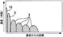
- FIG. 23 is a diagram illustrating a turn-off waveform of L load switching performed by a IGBT having a withstand voltage of 1200 V class in a device simulation.
- the waveform oscillates at a depth of 2 ⁇ m, but no oscillation occurs at 30 ⁇ m.
- n + -type buffer layer When a deep n + -type buffer layer of about 30 ⁇ m is formed by phosphorus diffusion, it takes 24 hours or more at a general heat treatment temperature such as 1100 ° C., and mass productivity is low.
- an accelerator such as a cyclotron or a bandegraph (for example, see Patent Document 1).
- the range when a silicon substrate is irradiated with protons at an acceleration voltage of 8 MeV, the range is about 480 ⁇ m and the half width is about 20 ⁇ m. In order to adjust the position of the range, it is possible not to directly shoot into the silicon substrate, but to shoot through the absorber, thereby reducing the irradiation energy and creating a broad proton peak near the silicon surface.
- a heat treatment is performed at 350 to 450 ° C. for 1 to 5 hours, whereby protons are activated and an n-type region can be formed.
- the proton activation rate is about 1% although it depends on the implantation conditions and heat treatment conditions.
- the mechanism by which protons become n-type donors is determined by the combined factors of implanted hydrogen atoms, crystal defects formed at the time of implantation, and oxygen atoms remaining on the substrate.
- the activation rate varies depending on the oxygen concentration and proton injection conditions.
- concentration of the n + -type buffer layer formed by proton implantation varies, leakage current and on-voltage variation increase, short circuit withstand capability, and the like occur.
- the present invention has been made to solve the above-described problems, and its purpose is to reduce leakage current, suppress oscillation during turn-off and recovery, and easily perform proton injection even in a general semiconductor factory.
- a semiconductor device capable of forming an n-type buffer layer and a method for manufacturing the same are obtained.
- a semiconductor device includes a semiconductor substrate, a p-type layer formed on a surface of the semiconductor substrate, and first and second n-type buffer layers formed on a back surface of the semiconductor substrate,
- the first n-type buffer layer is formed by multiple injections of protons having different acceleration voltages, has a plurality of peak concentrations with different depths from the back surface of the semiconductor substrate, and the second n-type buffer layer has Formed by implantation of phosphorus, the position of the peak concentration of phosphorus is shallower from the back surface of the semiconductor substrate than the position of the peak concentration of protons, the peak concentration of phosphorus is higher than the peak concentration of protons, It is characterized in that the proton concentration is higher than the phosphorus concentration at the position of the peak concentration.
- the first n-type buffer layer having a low concentration and a large diffusion depth formed by proton implantation can prevent oscillation during IGBT turn-off or diode recovery. Further, the depletion layer can be stopped by the high-concentration second n-type buffer layer into which phosphorus has been implanted, thereby preventing an increase in leakage current. Further, an n-type buffer layer can be easily formed by proton injection even in a general semiconductor factory without using a cyclotron.
- FIG. 7 is a cross-sectional view showing a semiconductor device according to Comparative Example 1.
- FIG. 7 is a diagram showing a back surface profile of a semiconductor device according to Comparative Example 1.
- FIG. 7 is sectional drawing which shows the semiconductor device which concerns on Embodiment 2 of this invention. It is a figure which shows the back surface profile of the semiconductor device which concerns on Embodiment 2 of this invention.
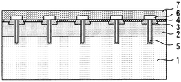
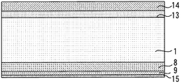
- FIG. 1 is a cross-sectional view showing a semiconductor device according to the first embodiment of the present invention.
- This semiconductor device is an IGBT.
- a p-type base layer 2 is formed on the surface of the n-type silicon substrate 1.
- An n + -type emitter layer 3 and a p + -type contact layer 4 are formed on the p-type base layer 2.
- a trench gate 5 is formed in a trench penetrating the p-type base layer 2 and the n + -type emitter layer 3 via a gate insulating film.
- An interlayer insulating film 6 is formed on the trench gate 5.
- An emitter electrode 7 is formed on the surface of the n-type silicon substrate 1 and connected to the p + -type contact layer 4.
- First and second n + -type buffer layers 8 and 9 are formed on the back surface of the n-type silicon substrate 1.
- the first n + -type buffer layer 8 is formed by a plurality of proton injections having different acceleration voltages.
- the second n + -type buffer layer 9 is formed by phosphorus implantation.
- a p-type collector layer 10 having a depth of about 1.0 ⁇ m is formed at a position shallower than the first and second n + -type buffer layers 8 and 9 from the back surface of the n-type silicon substrate 1.
- a collector electrode 11 is formed on the back surface of the n-type silicon substrate 1 and connected to the p-type collector layer 10.
- FIG. 2 is a diagram showing a back surface profile of the semiconductor device according to the first embodiment of the present invention.
- Protons in the first n + -type buffer layer 8 have a plurality of peak concentrations having different depths from the back surface of the n-type silicon substrate 1.
- the position of the peak concentration of phosphorus in the second n + -type buffer layer 9 is shallower from the back surface of the n-type silicon substrate 1 than the position of the peak concentration of proton in the first n + -type buffer layer 8.
- the peak concentration of phosphorus is higher than the peak concentration of protons.
- the proton concentration is higher than the phosphorus concentration at the position of the proton peak concentration.
- FIG. 3 to 10 are cross-sectional views showing the manufacturing steps of the semiconductor device according to the first embodiment of the present invention.
- the surface structure of the IGBT is formed by a normal surface process.
- the wafer thickness is about 700 ⁇ m, which is almost the same as the bare wafer.
- the back side of the n-type silicon substrate 1 is polished to a desired thickness by a grinder or wet etching.
- protons are implanted into the back surface of the n-type silicon substrate 1 a plurality of times at different acceleration voltages of 500 keV or more and 1.5 MeV or less using a general semiconductor manufacturing ion implantation apparatus.
- the range of protons is about 6 ⁇ m at 500 keV and about 30 ⁇ m at 1500 keV.
- proton activation is performed by furnace annealing at 350 ° C. to 450 ° C. to form the first n + -type buffer layer 8.
- phosphorus is implanted into a shallow region on the back surface of the n-type silicon substrate 1 at an acceleration voltage of 1 MeV or less.
- phosphorous activation is performed by laser annealing to form a second n + -type buffer layer 9.
- B is implanted into the back surface of the n-type silicon substrate 1.
- laser annealing is performed to form the p + -type contact layer 4.
- a collector electrode 11 such as Al / Ti / Ni / Au or AlSi / Ti / Ni / Au is formed on the back surface of the n-type silicon substrate 1 by sputtering.
- heat treatment at about 350 ° C. is performed to reduce ohmic contact between the collector electrode 11 and the n-type silicon substrate 1. At this time, by performing the heat treatment for proton activation in the same process, the heat treatment process can be reduced once, so that the processing cost can be reduced.
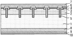
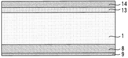
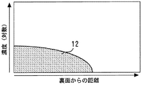
- FIG. 11 is a cross-sectional view showing a semiconductor device according to Comparative Example 1.
- FIG. 12 is a diagram showing a back surface profile of the semiconductor device according to Comparative Example 1.
- the n + -type buffer layer 12 is formed as deep as about 30 ⁇ m by proton injection using an accelerator such as a cyclotron or a bandegraph.
- the range is about 30 ⁇ m, and a deep buffer layer that can be expected to suppress the oscillation can be formed.
- the acceleration voltage can be increased up to about 1.5 MeV.
- a diffusion layer formed at a low acceleration voltage by an ion implantation apparatus for semiconductor production has a small half width, so that it is difficult to make a broad diffusion layer as produced by cycloton.
- the first n + -type buffer having a relatively broad profile as shown in FIG. 2 is obtained by performing proton injection multiple times with different acceleration voltages such as 500 keV, 1000 keV, and 1500 keV.
- Layer 8 can be formed.
- the concentration of the n-type layer may vary. Therefore, by forming the high-concentration second n + -type buffer layer 9 formed by phosphorus implantation near the back surface, it is possible to prevent the depletion layer from reaching the collector side when a voltage is applied, An increase in leakage current can be suppressed.
- Phosphorus has a larger atomic radius than protons, and many implantation damages occur due to collision of nuclei during implantation, and if the implantation profile of phosphorus overlaps with the proton implantation profile, it may affect proton donor formation. There is. Therefore, in this embodiment, the peak position is set so that the proton concentration is higher than the phosphorus concentration at the proton peak concentration position. Thereby, mutual interference can be prevented, and the first n + -type buffer layer 8 formed by proton activation can be set to a desired concentration.
- oscillation at the turn-off time of the IGBT can be prevented by the first n + -type buffer layer 8 having a low concentration and a large diffusion depth formed by proton implantation.
- the depletion layer can be stopped by the high-concentration second n + -type buffer layer 9 into which phosphorus is implanted, thereby preventing an increase in leakage current.
- the first n + -type buffer layer 8 is formed by performing proton implantation a plurality of times at different acceleration voltages using a general ion implantation apparatus for semiconductor production.
- the first n + -type buffer layer 8 can be easily formed by proton injection even in a general semiconductor factory without using a cyclotron.
- the profile of the first n + -type buffer layer 8 formed by proton injection a plurality of times can be brought close to a Gaussian distribution.
- the injection amount of the profile with the highest acceleration voltage among the proton injections of the plurality of times is the same as the injection amount of the profile with the next highest acceleration voltage.
- the injection amount of phosphorus is lower than the injection amount of protons
- activation of phosphorus is performed by laser annealing
- activation of protons is performed by furnace annealing at 350 ° C. to 450 ° C.
- the activation rate increases to about 70%.
- the activation rate of proton annealing by annealing is about 1%.
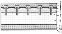
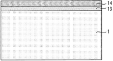
- FIG. FIG. 13 is a sectional view showing a semiconductor device according to the second embodiment of the present invention.
- This semiconductor device is a diode.
- a p-type anode layer 13 is formed on the surface of the n-type silicon substrate 1.
- An anode electrode 14 is formed on the surface of the n-type silicon substrate 1 and connected to the p-type anode layer 13.
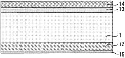
- first and second n + -type buffer layers 8 and 9 are formed on the back surface of the n-type silicon substrate 1.
- a cathode electrode 15 is formed on the back surface of the n-type silicon substrate 1 and connected to the second n + -type buffer layer 9.
- FIG. 14 is a diagram showing a back surface profile of the semiconductor device according to the second embodiment of the present invention. Similar to the first embodiment, protons in the first n + -type buffer layer 8 have a plurality of peak concentrations having different depths from the back surface of the n-type silicon substrate 1. The position of the peak concentration of phosphorus in the second n + -type buffer layer 9 is shallower from the back surface of the n-type silicon substrate 1 than the position of the peak concentration of proton in the first n + -type buffer layer 8. The peak concentration of phosphorus is higher than the peak concentration of protons. The proton concentration is higher than the phosphorus concentration at the position of the proton peak concentration.
- 15 to 20 are cross-sectional views showing the manufacturing steps of the semiconductor device according to the second embodiment of the present invention.
- the surface structure of the diode is formed by a normal surface process.
- the wafer thickness is about 700 ⁇ m, which is almost the same as the bare wafer.
- the back side of the n-type silicon substrate 1 is polished to a desired thickness by a grinder or wet etching.
- protons are implanted into the back surface of the n-type silicon substrate 1 at different acceleration voltages of 500 keV or more and 1.5 MeV or less using a general semiconductor manufacturing ion implantation apparatus.
- the range of protons is about 6 ⁇ m at 500 keV and about 30 ⁇ m at 1500 keV.
- proton activation is performed by furnace annealing at 350 ° C. to 450 ° C. to form the first n + -type buffer layer 8.
- phosphorus is implanted into a shallow region on the back surface of the n-type silicon substrate 1 at an acceleration voltage of 1 MeV or less.
- phosphorous activation is performed by laser annealing to form a second n + -type buffer layer 9.
- a cathode electrode 15 such as Al / Ti / Ni / Au or AlSi / Ti / Ni / Au is formed on the back surface of the n-type silicon substrate 1 by sputtering.
- heat treatment at about 350 ° C. is performed to reduce ohmic contact between the cathode electrode 15 and the n-type silicon substrate 1.
- the heat treatment process can be reduced once, so that the processing cost can be reduced.
- FIG. 21 is a cross-sectional view showing a semiconductor device according to Comparative Example 2.
- FIG. 22 is a diagram showing a back surface profile of the semiconductor device according to Comparative Example 2.
- the n + -type buffer layer 12 is formed as deep as about 30 ⁇ m by proton injection using an accelerator such as a cyclotron or a bandegraph.
- the depletion layer can be stopped by the high-concentration second n + -type buffer layer 9 into which phosphorus is implanted, thereby preventing an increase in leakage current.
- the first n + -type buffer layer 8 can be easily formed by proton injection even in a general semiconductor factory without using a cyclotron.
- the semiconductor substrate is not limited to being formed of silicon, but may be formed of a wide band gap semiconductor having a larger band gap than silicon.
- the wide band gap semiconductor is, for example, silicon carbide, a gallium nitride-based material, or diamond.
- a power semiconductor element formed of such a wide band gap semiconductor can be miniaturized because of its high voltage resistance and allowable current density.
- a semiconductor module incorporating this element can also be miniaturized.
- the heat resistance of the element is high, the heat dissipating fins of the heat sink can be miniaturized and the water cooling part can be air cooled, so that the semiconductor module can be further miniaturized.
- the power loss of the element is low and the efficiency is high, the efficiency of the semiconductor module can be increased.
- n-type silicon substrate semiconductor substrate
- 2 p-type base layer p-type layer
- 8 first n + -type buffer layer first n-type buffer layer
- 9 second n + -type buffer layer Second n-type buffer layer
- 11 collector electrode back electrode
- 13 p-type anode layer p-type layer
- 15 cathode electrode back electrode
Landscapes
- Electrodes Of Semiconductors (AREA)
- Physics & Mathematics (AREA)
- Electromagnetism (AREA)
- Optics & Photonics (AREA)
Abstract
Priority Applications (5)
| Application Number | Priority Date | Filing Date | Title |
|---|---|---|---|
| DE112015006307.2T DE112015006307B4 (de) | 2015-03-13 | 2015-03-13 | Verfahren einer Fertigung einer Halbleitervorrichtung |
| US15/545,732 US10176994B2 (en) | 2015-03-13 | 2015-03-13 | Semiconductor device and method of manufacturing the same |
| JP2017505779A JP6519649B2 (ja) | 2015-03-13 | 2015-03-13 | 半導体装置及びその製造方法 |
| CN201580077781.7A CN107431087B (zh) | 2015-03-13 | 2015-03-13 | 半导体装置及其制造方法 |
| PCT/JP2015/057539 WO2016147264A1 (fr) | 2015-03-13 | 2015-03-13 | Dispositif à semi-conducteurs et procédé de fabrication de celui-ci |
Applications Claiming Priority (1)
| Application Number | Priority Date | Filing Date | Title |
|---|---|---|---|
| PCT/JP2015/057539 WO2016147264A1 (fr) | 2015-03-13 | 2015-03-13 | Dispositif à semi-conducteurs et procédé de fabrication de celui-ci |
Publications (1)
| Publication Number | Publication Date |
|---|---|
| WO2016147264A1 true WO2016147264A1 (fr) | 2016-09-22 |
Family
ID=56918545
Family Applications (1)
| Application Number | Title | Priority Date | Filing Date |
|---|---|---|---|
| PCT/JP2015/057539 Ceased WO2016147264A1 (fr) | 2015-03-13 | 2015-03-13 | Dispositif à semi-conducteurs et procédé de fabrication de celui-ci |
Country Status (5)
| Country | Link |
|---|---|
| US (1) | US10176994B2 (fr) |
| JP (1) | JP6519649B2 (fr) |
| CN (1) | CN107431087B (fr) |
| DE (1) | DE112015006307B4 (fr) |
| WO (1) | WO2016147264A1 (fr) |
Cited By (8)
| Publication number | Priority date | Publication date | Assignee | Title |
|---|---|---|---|---|
| JP2018078216A (ja) * | 2016-11-10 | 2018-05-17 | 三菱電機株式会社 | 半導体装置およびその製造方法 |
| DE102018205274A1 (de) | 2017-06-20 | 2018-12-20 | Mitsubishi Electric Corporation | Halbleitervorrichtung und verfahren zu deren herstellung |
| CN109560160A (zh) * | 2017-09-25 | 2019-04-02 | 艾普凌科有限公司 | 紫外线受光元件和紫外线受光元件的制造方法 |
| US10593789B2 (en) | 2017-09-29 | 2020-03-17 | Mitsubishi Electric Corporation | Semiconductor apparatus and method of manufacturing the same |
| JP2020107917A (ja) * | 2016-12-27 | 2020-07-09 | 三菱電機株式会社 | 半導体装置の製造方法 |
| JP2022035157A (ja) * | 2020-08-20 | 2022-03-04 | 三菱電機株式会社 | 半導体装置および半導体装置の製造方法 |
| US11894426B2 (en) | 2019-10-17 | 2024-02-06 | Fuji Electric Co., Ltd. | Semiconductor device and manufacturing method for semiconductor device |
| US12191358B2 (en) | 2019-08-09 | 2025-01-07 | Fuji Electric Co., Ltd. | Semiconductor device |
Families Citing this family (9)
| Publication number | Priority date | Publication date | Assignee | Title |
|---|---|---|---|---|
| CN106991221B (zh) * | 2017-03-24 | 2020-04-24 | 清华大学 | 一种基于igbt器件瞬态物理过程的分段折线建模方法 |
| JP7070303B2 (ja) * | 2018-10-04 | 2022-05-18 | 三菱電機株式会社 | 半導体装置 |
| CN113053746B (zh) * | 2019-12-27 | 2024-07-09 | 株洲中车时代半导体有限公司 | 一种低压igbt器件的制备方法 |
| CN111933703B (zh) * | 2020-10-12 | 2021-01-29 | 中芯集成电路制造(绍兴)有限公司 | 一种绝缘栅双极型晶体管及其形成方法 |
| JP7415913B2 (ja) * | 2020-12-28 | 2024-01-17 | 三菱電機株式会社 | 半導体装置及びその製造方法 |
| CN116978937A (zh) * | 2021-02-07 | 2023-10-31 | 华为技术有限公司 | 半导体器件及相关模块、电路、制备方法 |
| CN113206013A (zh) * | 2021-04-27 | 2021-08-03 | 上海积塔半导体有限公司 | 具有背面缓冲层结构的igbt器件及其制备方法 |
| CN113644123B (zh) * | 2021-06-28 | 2024-09-06 | 华为技术有限公司 | 半导体器件及相关芯片和制备方法 |
| CN113851379A (zh) * | 2021-09-24 | 2021-12-28 | 上海积塔半导体有限公司 | Igbt器件及其制作方法 |
Citations (4)
| Publication number | Priority date | Publication date | Assignee | Title |
|---|---|---|---|---|
| JP2002507058A (ja) * | 1998-03-09 | 2002-03-05 | ハリス コーポレイション | 低温直接ボンディングにより形成可能な装置 |
| JP4128777B2 (ja) * | 2000-05-05 | 2008-07-30 | インターナショナル・レクチファイヤー・コーポレーション | 絶縁ゲートバイポーラトランジスタ(igbt)及びその製造方法 |
| JP2013138172A (ja) * | 2011-11-30 | 2013-07-11 | Denso Corp | 半導体装置 |
| WO2013147274A1 (fr) * | 2012-03-30 | 2013-10-03 | 富士電機株式会社 | Procédé de fabrication pour dispositif à semi-conducteurs |
Family Cites Families (10)
| Publication number | Priority date | Publication date | Assignee | Title |
|---|---|---|---|---|
| US6239466B1 (en) * | 1998-12-04 | 2001-05-29 | General Electric Company | Insulated gate bipolar transistor for zero-voltage switching |
| JP5365009B2 (ja) * | 2008-01-23 | 2013-12-11 | 富士電機株式会社 | 半導体装置およびその製造方法 |
| JP5374883B2 (ja) * | 2008-02-08 | 2013-12-25 | 富士電機株式会社 | 半導体装置およびその製造方法 |
| US8766413B2 (en) * | 2009-11-02 | 2014-07-01 | Fuji Electric Co., Ltd. | Semiconductor device and method for manufacturing semiconductor device |
| KR20120140411A (ko) * | 2011-06-21 | 2012-12-31 | (주) 트리노테크놀로지 | 전력 반도체 소자 및 그 제조 방법 |
| EP2782121B1 (fr) * | 2011-11-15 | 2021-01-06 | Fuji Electric Co., Ltd. | Dispositif semi-conducteur et procédé de fabrication du dispositif semi-conducteur |
| EP2793266B1 (fr) | 2011-12-15 | 2020-11-11 | Fuji Electric Co., Ltd. | Procédé de fabrication d'un dispositif semi-conducteur |
| CN103946985B (zh) | 2011-12-28 | 2017-06-23 | 富士电机株式会社 | 半导体装置及半导体装置的制造方法 |
| EP2913854B1 (fr) * | 2012-10-23 | 2020-05-27 | Fuji Electric Co., Ltd. | Dispositif à semi-conducteur et son procédé de fabrication |
| JP6311723B2 (ja) | 2013-12-16 | 2018-04-18 | 富士電機株式会社 | 半導体装置および半導体装置の製造方法 |
-
2015
- 2015-03-13 WO PCT/JP2015/057539 patent/WO2016147264A1/fr not_active Ceased
- 2015-03-13 CN CN201580077781.7A patent/CN107431087B/zh active Active
- 2015-03-13 US US15/545,732 patent/US10176994B2/en active Active
- 2015-03-13 DE DE112015006307.2T patent/DE112015006307B4/de active Active
- 2015-03-13 JP JP2017505779A patent/JP6519649B2/ja active Active
Patent Citations (4)
| Publication number | Priority date | Publication date | Assignee | Title |
|---|---|---|---|---|
| JP2002507058A (ja) * | 1998-03-09 | 2002-03-05 | ハリス コーポレイション | 低温直接ボンディングにより形成可能な装置 |
| JP4128777B2 (ja) * | 2000-05-05 | 2008-07-30 | インターナショナル・レクチファイヤー・コーポレーション | 絶縁ゲートバイポーラトランジスタ(igbt)及びその製造方法 |
| JP2013138172A (ja) * | 2011-11-30 | 2013-07-11 | Denso Corp | 半導体装置 |
| WO2013147274A1 (fr) * | 2012-03-30 | 2013-10-03 | 富士電機株式会社 | Procédé de fabrication pour dispositif à semi-conducteurs |
Cited By (15)
| Publication number | Priority date | Publication date | Assignee | Title |
|---|---|---|---|---|
| CN108074977A (zh) * | 2016-11-10 | 2018-05-25 | 三菱电机株式会社 | 半导体装置及其制造方法 |
| JP2018078216A (ja) * | 2016-11-10 | 2018-05-17 | 三菱電機株式会社 | 半導体装置およびその製造方法 |
| US10347715B2 (en) | 2016-11-10 | 2019-07-09 | Mitsubishi Electric Corporation | Semiconductor device having improved safe operating areas and manufacturing method therefor |
| JP2020107917A (ja) * | 2016-12-27 | 2020-07-09 | 三菱電機株式会社 | 半導体装置の製造方法 |
| DE102018205274A1 (de) | 2017-06-20 | 2018-12-20 | Mitsubishi Electric Corporation | Halbleitervorrichtung und verfahren zu deren herstellung |
| US10263102B2 (en) | 2017-06-20 | 2019-04-16 | Mitsubishi Electric Corporation | Semiconductor device and method of manufacturing the same |
| DE102018205274B4 (de) | 2017-06-20 | 2022-07-14 | Mitsubishi Electric Corporation | Halbleitervorrichtung und verfahren zu deren herstellung |
| CN109560160A (zh) * | 2017-09-25 | 2019-04-02 | 艾普凌科有限公司 | 紫外线受光元件和紫外线受光元件的制造方法 |
| US10593789B2 (en) | 2017-09-29 | 2020-03-17 | Mitsubishi Electric Corporation | Semiconductor apparatus and method of manufacturing the same |
| US12191358B2 (en) | 2019-08-09 | 2025-01-07 | Fuji Electric Co., Ltd. | Semiconductor device |
| US11894426B2 (en) | 2019-10-17 | 2024-02-06 | Fuji Electric Co., Ltd. | Semiconductor device and manufacturing method for semiconductor device |
| US12369370B2 (en) | 2019-10-17 | 2025-07-22 | Fuji Electric Co., Ltd. | Semiconductor device and manufacturing method for semiconductor device |
| JP2022035157A (ja) * | 2020-08-20 | 2022-03-04 | 三菱電機株式会社 | 半導体装置および半導体装置の製造方法 |
| US11695065B2 (en) | 2020-08-20 | 2023-07-04 | Mitsubishi Electric Corporation | Semiconductor device and method of manufacturing semiconductor device |
| JP7528628B2 (ja) | 2020-08-20 | 2024-08-06 | 三菱電機株式会社 | 半導体装置および半導体装置の製造方法 |
Also Published As
| Publication number | Publication date |
|---|---|
| DE112015006307T5 (de) | 2017-12-21 |
| CN107431087A (zh) | 2017-12-01 |
| JP6519649B2 (ja) | 2019-05-29 |
| JPWO2016147264A1 (ja) | 2017-09-07 |
| US20180019131A1 (en) | 2018-01-18 |
| CN107431087B (zh) | 2020-12-11 |
| DE112015006307B4 (de) | 2026-01-15 |
| US10176994B2 (en) | 2019-01-08 |
Similar Documents
| Publication | Publication Date | Title |
|---|---|---|
| JP6519649B2 (ja) | 半導体装置及びその製造方法 | |
| US11469297B2 (en) | Semiconductor device and method for producing semiconductor device | |
| CN109103247B (zh) | 半导体装置及其制造方法 | |
| CN107195677B (zh) | 半导体装置和半导体装置的制造方法 | |
| US11152224B2 (en) | Semiconductor device with field stop layer and semiconductor device manufacturing method thereof | |
| JP6078961B2 (ja) | 半導体装置の製造方法 | |
| JP5365009B2 (ja) | 半導体装置およびその製造方法 | |
| EP2320451B1 (fr) | Diode à récupération rapide | |
| CN105280485B (zh) | 制造包括场停止区的半导体器件的方法 | |
| US10497570B2 (en) | Method for manufacturing semiconductor device having buffer layer | |
| CN106463528A (zh) | 碳化硅半导体装置的制造方法 | |
| JP2018078216A (ja) | 半導体装置およびその製造方法 | |
| CN105830220B (zh) | 半导体装置的制造方法 | |
| US9991336B2 (en) | Semiconductor device, method for manufacturing the same, and power conversion system | |
| JP6702467B2 (ja) | 半導体装置及びその製造方法 | |
| JP6268117B2 (ja) | 半導体装置およびその製造方法、並びに電力変換システム | |
| CN107275395A (zh) | 半导体装置及其制造方法 |
Legal Events
| Date | Code | Title | Description |
|---|---|---|---|
| 121 | Ep: the epo has been informed by wipo that ep was designated in this application |
Ref document number: 15885362 Country of ref document: EP Kind code of ref document: A1 |
|
| ENP | Entry into the national phase |
Ref document number: 2017505779 Country of ref document: JP Kind code of ref document: A |
|
| WWE | Wipo information: entry into national phase |
Ref document number: 15545732 Country of ref document: US |
|
| WWE | Wipo information: entry into national phase |
Ref document number: 112015006307 Country of ref document: DE |
|
| 122 | Ep: pct application non-entry in european phase |
Ref document number: 15885362 Country of ref document: EP Kind code of ref document: A1 |
|
| WWG | Wipo information: grant in national office |
Ref document number: 112015006307 Country of ref document: DE |