WO2016147351A1 - Système informatique, procédé et ordinateur hôte - Google Patents
Système informatique, procédé et ordinateur hôte Download PDFInfo
- Publication number
- WO2016147351A1 WO2016147351A1 PCT/JP2015/058100 JP2015058100W WO2016147351A1 WO 2016147351 A1 WO2016147351 A1 WO 2016147351A1 JP 2015058100 W JP2015058100 W JP 2015058100W WO 2016147351 A1 WO2016147351 A1 WO 2016147351A1
- Authority
- WO
- WIPO (PCT)
- Prior art keywords
- logical
- limited
- area
- vertex
- chunk
- Prior art date
- Legal status (The legal status is an assumption and is not a legal conclusion. Google has not performed a legal analysis and makes no representation as to the accuracy of the status listed.)
- Ceased
Links
Images






Classifications
-
- G—PHYSICS
- G06—COMPUTING OR CALCULATING; COUNTING
- G06F—ELECTRIC DIGITAL DATA PROCESSING
- G06F3/00—Input arrangements for transferring data to be processed into a form capable of being handled by the computer; Output arrangements for transferring data from processing unit to output unit, e.g. interface arrangements
- G06F3/06—Digital input from, or digital output to, record carriers, e.g. RAID, emulated record carriers or networked record carriers
-
- G—PHYSICS
- G06—COMPUTING OR CALCULATING; COUNTING
- G06F—ELECTRIC DIGITAL DATA PROCESSING
- G06F12/00—Accessing, addressing or allocating within memory systems or architectures
-
- G—PHYSICS
- G06—COMPUTING OR CALCULATING; COUNTING
- G06F—ELECTRIC DIGITAL DATA PROCESSING
- G06F12/00—Accessing, addressing or allocating within memory systems or architectures
- G06F12/02—Addressing or allocation; Relocation
Definitions
- the present invention relates to a computer system using a nonvolatile semiconductor memory.
- a storage device using a nonvolatile memory as a storage medium is used instead of or in addition to an HDD (Hard Disk Drive).
- a nonvolatile memory is, for example, a NAND flash memory.
- a storage device using a non-volatile memory as a storage medium is considered to be superior in power saving, access time, and the like as compared to a storage device having a plurality of small disk drives.
- Flash memory includes a plurality of blocks in a memory chip.
- a block is a storage area in a unit for erasing data collectively, and a page is a storage area in a unit for reading and writing data.
- a plurality of pages are provided in one block.
- flash memory cannot directly rewrite stored data due to its characteristics. When the stored data is rewritten, the flash memory saves the stored valid data in another block and then erases the stored data in units of blocks. Then, the flash memory writes data to the erased block. As described above, rewriting of data in the flash memory is accompanied by erasure of data for each block. By erasing data, the memory chip is consumed. For this reason, the number of erasable times is defined for each block.
- the controller specifies a physical area assigned to a logical chunk assigned to a logical page according to the logical address of the data write destination, and writes data to the specified physical area Is known (Patent Document 1).
- graph processing is known as a technique for efficiently processing objects that dramatically increase due to the development of the Internet environment (Patent Document 2).
- the number of objects processed in graph processing is increasing year by year.
- the data processed by the storage device is increasing year by year.
- a storage device including a nonvolatile memory when enormous data processing is performed, if data is written in a disorderly manner, the data rewriting operation increases, GC occurs frequently, and the lifetime of the nonvolatile memory may be reduced.
- a computer system includes a storage device and a host computer connected to the storage device.
- the storage device includes a non-volatile memory and a controller connected to the non-volatile memory and the host computer.
- the host computer includes a storage device and a processor connected to the storage device and the storage apparatus.
- the controller stores limited information related to the size of the first limited logical area that is a part of the logical storage area of the nonvolatile memory, and based on the limited information, the first physical that is a part of the physical storage area of the nonvolatile memory.
- the storage area is associated with the first limited logical area.
- the controller transmits the limited information to the host computer.
- the processor executes the first process and generates first process data by the first process.
- the processor calculates a first logical address range indicating the first limited logical area based on the limited information.
- the processor transmits the first write command specifying the first logical address within the first logical address range and the first processing data to the storage device.
- the controller assigns the first physical address in the first physical storage area to the first logical address, and writes the first processing data in the area indicated by the first physical address.
- the processor transmits a read command designating the first logical address to the storage device.
- the controller reads the first processing data from the area indicated by the first physical address.
- the processor transmits a specific command indicating that the first logical address range is unnecessary to the storage device.
- the controller erases the first processing data after receiving the specific command.
- FIG. 1 shows a configuration of a computer system according to the present embodiment. An example of information stored in the main memory 122 is shown. It is a figure which shows the structure of the program regarding a graph process.
- 3 is a diagram showing a connection state inside the nonvolatile memory device 101.
- FIG. It is a figure which shows the relationship between a logical page and a chunk. It is a figure for demonstrating the logical-physical conversion by the controller 112.
- FIG. It is a figure explaining the relationship of a chunk, a chunk set, and a chunk group. It is a figure explaining the grouping process of the vertex 1101.
- FIG. 1 shows a configuration of a computer system according to the present embodiment. An example of information stored in the main memory 122 is shown. It is a figure which shows the structure of the program regarding a graph process.
- 3 is a diagram showing a connection state inside the nonvolatile memory device 101.
- FIG. It is a figure which shows the relationship between a logical page and
- FIG. 11 is a diagram for describing grouping processing and writing processing of a message 1102.
- FIG. 10 is a diagram for explaining a message 1102 reading process. A flowchart of the write range control process according to this embodiment will be described. It is a flowchart of an initialization process. It is a flowchart of a writing process.
- information may be described in terms of “kkk list”, “kkk table”, and “kkk information”, but the information may be expressed in any data structure.
- the “kkk list”, “kkk table”, and “kkk information” can be replaced by any name to indicate that they do not depend on the data structure.
- the expressions “ID”, “number”, and “identifier” are used, but other types of identification information may be used instead of or in addition to these.
- the process may be described using “program” as a subject.
- the program is executed by the processor, so that the determined process can be appropriately performed with storage resources (for example, memory) and / or Alternatively, since the processing is performed using a communication interface device (for example, a communication port), the subject of processing may be a processor. On the contrary, the processing whose subject is the processor can be interpreted as being executed by executing one or more programs.
- a host computer performs BSP (Bulk Synchronous Parallel) graph processing as a data operation method.
- BSP Bit Synchronous Parallel
- FIG. 1 is a diagram for explaining the concept of graph processing.
- the graph is a concept showing vertices and edges representing connections between the vertices.
- processing is performed for each vertex, and a message is sent along the edge.
- an edge connecting the vertex V1 and the vertices V2 and V3 indicates that the vertex V1 notifies the vertices V2 and V3 of a message.
- vertex V2 sends a message to vertex V4
- vertex V3 sends a message to vertex V2
- vertex V4 sends a message to vertices V1 and V3.
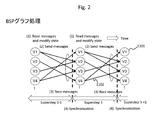
- FIG. 2 is a diagram for explaining BSP graph processing.
- the vertex 1101 includes a vertex ID for identifying the vertex 1101.
- V1 to V4 are vertex IDs.
- Data output during the processing of each vertex 1101 is a message 1102.
- the message 1102 is attached with a destination indicating one vertex 1101 that is related to the output source vertex 1101.
- the destination vertex receives the message 1102 and performs processing.
- the process from the start of the processing of the first vertex 1101 to the completion of the processing of the last vertex 1101 is called a super step. Synchronization is performed for each super step.
- the vertex inputs a message addressed to itself (read messages), and the vertex executes a process to update the state of the vertex (modify state).
- the vertex outputs a message for the next destination vertex (send message).
- the destination vertex receives the output message (Recv messages). (4)
- the super step S is completed (synchronization), and the process proceeds to the next super step S1.
- the message size is smaller than the block size of the non-volatile memory.
- data is frequently fragmented and GC is frequently performed.
- valid data in the erase block must be moved to another block. Therefore, extra fragmentation occurs when fragmentation occurs. That is, the number of block erasures increases and the lifetime of the nonvolatile storage medium is shortened.
- the computer system according to the present embodiment can reduce the number of block erasures by reducing GC by writing a plurality of messages to a specific physical storage area and erasing the plurality of messages at a time. It is possible to prevent the life of the product from being shortened. Furthermore, it is possible to prevent a decrease in the access performance of the nonvolatile memory due to the GC.
- FIG. 3 shows a configuration of a computer system according to the present embodiment.
- the computer system is a system in which a nonvolatile memory device 101 and a host computer (hereinafter referred to as a host) 102 are connected via a communication network.
- the non-volatile memory device 101 and the host 102 may communicate with the same communication protocol (for example, PCI Express (registered trademark)) as the communication protocol in the non-volatile memory device 101 and the communication protocol in the host 102 or different communication. Communication may be performed using a protocol (for example, Fiber Channel).
- the computer system may be a converged system in which the nonvolatile memory device 101 and the host 102 are housed in one housing.
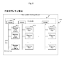
- the nonvolatile memory device 101 is, for example, a storage media drive (for example, SSD; Solid State Drive) having one or more memory chips 111. Further, the nonvolatile memory device 101 may be a large-scale memory system having a plurality of nonvolatile memory devices 101. In the present embodiment, the nonvolatile memory device 101 is described as a media drive having one or more memory chips 111, a controller 112, a chunk information register 114, and a host I / F 118. These elements may be connected to each other by, for example, a bus (for example, a PCI Express bus).
- a bus for example, a PCI Express bus
- the memory chip 111 is a NAND flash memory in this embodiment. Therefore, the memory chip 111 is composed of a plurality of blocks, and each block is composed of a plurality of physical pages. Data is read / written for each physical page and data is erased for each block. That is, a physical page is a data writing unit, and a block is a data erasing unit.
- the memory chip 111 is replaced with other types of non-volatile memories (for example, MRAM (Magnetoretic Random Access Memory), ReRAM (Resistant Random Access Memory), or FeRAM (Ferroelectric Random Memory) instead of NAND flash memory. Good.
- the controller 112 is a module including a CPU (Central Processing Unit) (for example, a CPU itself or a module including a CPU and dedicated hardware such as DMA).
- the controller 112 performs processing in response to a request from the host 102.
- the controller 112 controls data transfer within the nonvolatile memory device 101.
- a CPU Central Processing Unit
- DMA dedicated hardware
- the chunk information register 114 is a storage area provided in a memory (not shown) in the nonvolatile memory device 101.
- the memory may be a volatile memory or a non-volatile memory.
- the memory is, for example, a DRAM (Dynamic Random Access Memory). Chunk information described later is stored in the chunk information register.
- the host I / F 113 is an interface device connected to the host 102.
- the host 102 includes a CPU 121, a main memory 122, and a nonvolatile memory I / F 123.
- the CPU 121 controls the operation of the host 102.
- the main memory 122 is a memory that the host 102 has.
- the main memory 122 is, for example, a DRAM, but other types of memory may be employed instead of the DRAM 122.
- the nonvolatile memory I / F 123 is an interface device connected to the host I / F 113 of the nonvolatile memory device 101.
- the host 102 may have a non-volatile memory (hereinafter, program memory) that stores a program executed by the CPU 121.
- program memory non-volatile memory
- a program may be loaded from the program memory into the main memory 122 and the program loaded into the main memory 122 may be executed by the CPU 121. There may be no program memory, and a program executed by the CPU 121 may be loaded from the memory chip 111 of the nonvolatile memory device 101 to the main memory 122.
- the host 102 may be connected to an input device (not shown) for inputting data such as a user code (to be described later) by the user and an output device (not shown) for displaying the processing result to the user.
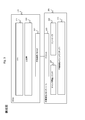
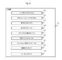
- FIG. 4 shows an example of information stored in the main memory 122 of the host 102.
- the main memory 122 includes a user code program 221, a graph framework (graph FW) program 222, a current address table 223, a previous address table 224, a chunk set allocation table 225, a free chunk set list 226, and a chunk set.
- An empty list table 227 and management middleware 228 are stored. As described above, these pieces of information may be stored in the program memory, or may be temporarily read from other places into the main memory 122 and used.
- a working area 229 for reading data necessary for graph processing is secured in the main memory 122.
- the user code program 221 is a program that specifies the contents of the graph processing by the user code input by the user.
- the graph FW program 222 is a program that executes graph processing.
- the management middleware 228 is a program that controls these programs 221 and 222, and is, for example, an OS.
- the user code program 221 specifies the size of the logical address according to the input from the user to the graph framework program 222.
- the graph framework program 222 requests the management middleware 228 for the specified logical address size.
- the management middleware 228 secures a storage area of the usable memory chip 111 based on the size of the logical address included in the request, and displays the range of usable logical addresses (start logical address and end logical address) in the graph frame.
- the work program 222 is notified. The description of each information 223 to 227 will be described later.
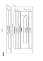
- FIG. 5 shows the configuration of a program related to graph processing.
- the user code program 221 and the graph framework program 222 are executed on the management middleware 228.
- the user code program 221 includes each vertex calculation processing unit 301.
- the graph framework program 222 includes a calculation processing order control unit 311, a calculation processing unit 312, a data communication processing unit 313, a writing processing unit 314, and a reading processing unit 315.
- the write processing unit 314 includes a grouping processing unit 321 and an address management unit 322. Each of these units is, for example, a program module.
- Each vertex calculation processing unit 301 is designated by a user code and indicates processing of each vertex.
- the calculation processing order control unit 311 controls the order of calculation processing in the calculation processing unit 312.
- the calculation processing unit 312 executes the processing of each vertex calculation processing unit 301.
- the data communication processing unit 313 controls message communication between 312 and 314.
- the writing processing unit 314 controls writing of data to the nonvolatile memory.
- the grouping processing unit 321 groups data.
- the address management unit 322 manages logical addresses.
- the read processing unit 315 controls reading of data from the nonvolatile memory.
- FIG. 6 is a diagram showing a connection state inside the nonvolatile memory device 101.
- the controller 112 has a plurality of DMA (Direct Memory Access) 115.
- the DMA 115 is a hardware circuit that controls data transfer.
- Each DMA 115 is connected to a plurality of memory chips 111 via a bus 116.
- a plurality of DMAs 115 in the controller 112 may be described with DMAID (#) attached.
- the controller 112 has 16 DMAs, DMA # 0 to DMA # 15.
- CEID (#) may be attached to a plurality of memory chips 111 connected to each DMA.
- 16 memory chips 111, CE # 0 to CE # 15 are connected to each DMA.
- the controller 112 may not have the DMA 115. In this case, the controller 112 controls data transfer in the nonvolatile memory device 101.
- FIG. 7 is a diagram showing the relationship between logical pages and chunks.
- the controller 112 sets a chunk 920 and a chunk group 960 including a plurality of chunks 920.
- the chunk group 960 is a matrix of a plurality of chunks 920.
- the controller 112 assigns each memory chip 111 to one chunk 920.
- the number of chunks (number of horizontal chunks) arranged in the horizontal (row) direction of the chunk group 960 corresponds to the number of DMAs 115 (16).
- the number of chunks arranged in the vertical (column) direction of the chunk group 960 corresponds to the number of memory chips 111 connected to one DMA 115 via the bus (the number of CEs, 16).
- the controller 112 defines each row in the chunk group 960 as a chunk set (see FIG. 9).
- the number of vertical chunks is the same as the number of chunk sets, and the number of horizontal chunks is the same as the number of chunks in each chunk set.
- the controller 112 sets a plurality of logical pages 922 in each chunk 920.
- the controller 112 associates a logical address with each logical page.
- the controller 112 manages the logical page 922 with the same size as the physical page in each memory chip 111, but may manage it with a different size.
- the controller 112 allocates a plurality of logical blocks 925 to each chunk 920.
- the logical block 925 is managed with the same size as the physical block 930 in each memory chip 111, but may be managed with a different size.
- the controller 112 allocates consecutive chunk numbers to the chunks 920 in the chunk group 960. For example, the controller 112 chunks chunks 960 in the chunk group 960 so that each chunk 920 in the first row is chunks # 00 to # 15 and each chunk 920 in the second row is chunks # 16 to # 31. Allocate 00 to # 255.
- the controller 112 assigns a logical block 925 to each chunk 920 in the chunk group 960. For example, the controller 112 assigns one logical block (B # 00) to the first column chunk (CHUNK # 00) in the first row, and then assigns it to the second column chunk (CHUNK # 01) in the first row. After allocating one logical block (B # 01) and allocating one logical block (B # 015) to the last column chunk (CHUNK # 015) of the first row, the first column chunk (second row) One logical block is allocated to CHUNK # 016).
- the controller 112 assigns logical blocks one by one to the last (16) column chunk (CHUNK # 225) of the last (16) row, and then again starts from the first chunk (CHUNK # 00) of the chunk group.
- a plurality of logical blocks are allocated to all the chunks 920 in the chunk group 960, such that the second logical block is allocated. That is, the controller 112 first assigns the first logical block in order of the chunk number to all chunks 920 in the chunk group 960, and then assigns the second logical block in order of the chunk number. Allocate logical blocks until each chunk is full.
- Controller 112 allocates logical page 922 to logical block 925.
- the number of chunk interleaved LPs is the number of logical pages 922 continuously allocated to each chunk 920.
- the number of chunk interleaved LPs is two.
- the controller 112 assigns two logical pages # 0 and # 1 to the first logical block (B # 00) in the first chunk in the chunk group in the order of logical page numbers.
- Logical pages # 2 and # 3 are allocated to the first logical block (B # 01) in the two-column chunk, and the first logical block (B # 15) in the fifteenth column of the first row is allocated.
- logical pages # 31 and 32 following the first logical block (B # 00) in the chunk of the first column in the first row are allocated.
- the controller 112 assigns all logical pages to the first logical block (B # 00 to 15) of each chunk in the first row, and then the first logical in the second row and each column. Assign logical pages to blocks in the same way.
- the controller 112 assigns a logical page to the first logical block of each column in the last row in the same manner, and then similarly assigns a logical page to the second logical block of each column in the first row. Assign.
- the controller 112 allocates logical pages 922 to each chunk 920 in the chunk group 960 up to a predetermined number of LPs in the chunk group.
- the number of LPs in the chunk group is, for example, a value (integer value) obtained by dividing the logical page number that can be arranged in the chunk group by the number of chunks in the chunk group in order to uniformly arrange the number of logical pages in each chunk. It may be a value obtained by multiplying the number of vertical chunks by the number of horizontal chunks.
- controller 112 identifies the corresponding chunk from the logical address.
- the controller 112 includes the page size of the logical page, the number of LPs in the chunk group 960, the number of LPs in the logical block 925, the number of horizontal chunks in the chunk group 960 (number of chunk sets, number of DMAs), chunk group The number of vertical chunks in 960 (number of chunks in chunk set, number of chunks connected to one DMA) and number of chunk interleaved LPs are stored.
- the controller 112 corresponds to each logical address, the logical page number (#), the chunk group number (#), the intra-chunk group logical page number (#), the intra-chunk group logical page number (#), The horizontal chunk number (#) and the vertical chunk number (#) are calculated.
- the calculation method of these values is as follows.
- Logical page number (#) logical address / page size
- chunk group number (#) logical page number (#) / number of LPs in chunk group
- LP number in chunk group (#) LP Number% Number of LPs in chunk group
- Vertical chunk number (#) (Number of LPs in chunk group / (Number of LPs in logical block * Number of horizontal chunks))% Number of vertical chunks in chunk group)
- Horizontal chunk number (#) (LP number in chunk / number of chunk interleaved LPs)% Number of horizontal chunks in chunk group
- the controller 112 is based on the vertical chunk number (#) and the horizontal chunk number (#). You may calculate the chunk number (#) which can specify each chunk uniquely within a chunk group.
- the controller 112 can specify a chunk from a logical address using the above formula.
- controller 112 transmits chunk information to the host 102.
- the host 102 can determine the range of logical addresses corresponding to each chunk set using the chunk information transmitted from the controller 112.
- FIG. 8 is a diagram for explaining logical-physical conversion by the controller 112.
- the memory chip 111 includes a plurality of physical blocks. Each physical block includes a plurality of physical pages.
- a logical page may be described as an L page and a physical page as a P page.
- the host 102 determines the logical address 911 based on the chunk information, designates the logical address 911, and transmits a command to the nonvolatile memory 101.
- the controller 112 receives a write command designating a logical address from the host 102, the controller 112 identifies a logical page and chunk corresponding to the logical address, and selects a free physical block from the memory chip 111 corresponding to the chunk. . Then, the controller 112 allocates a free physical page 933 from the top in the selected physical block 930 to the logical page 922. Thereby, the storage location of the write data is determined.
- the controller 112 identifies L page # 0 and chunk # 0 corresponding to LBA0x00, and an empty block in the memory chip # 0 corresponding to chunk # 0 # 00 is selected, P page # 00 in block # 00 is selected, P page # 00 is assigned to L page # 00, and write data according to the write command is written to P page # 0.
- the controller 112 assigns the memory chip 111 and the chunk 920 on a one-to-one basis.
- the present invention is not limited to this mode.
- the controller 112 erases data for each physical block 930 that is an erase unit. In this case, the controller 112 determines whether or not the number of free physical blocks has fallen below a preset threshold value, and when it falls, the valid page in the physical block having the highest invalid page rate is copied to another physical block. The GC is executed. The controller 112 erases data in the physical block that has become all invalid pages by GC, thereby making the physical page in the physical block an empty page in which data can be stored.
- the write data written in different chunks 920 is always stored in different physical blocks 930.
- the chunk information is notified from the controller 112 to the host 102.
- the host 102 can select the chunk set of the write data storage destination.
- the host 102 can store unnecessary data in a single chunk set based on preset conditions. Specifically, a plurality of data that becomes unnecessary and invalidated at the first timing are collectively stored in a plurality of physical blocks 930 corresponding to the first chunk set, erased collectively, and made into empty blocks. be able to. Thereby, GC can be reduced.
- the host 102 can store unnecessary data based on different conditions in another chunk set. Data that becomes unnecessary and invalidated at the first timing can be stored in the first chunk set, and data that becomes unnecessary and invalidated at the second timing can be stored in the second chunk set. Therefore, it is possible to prevent data that becomes unnecessary and invalidated at the first timing and data that becomes unnecessary and invalidated at the second timing from being stored in the same physical block.
- the controller 112 transfers the write data to each memory chip 111 allocated in the chunk set. Can be distributed and stored. As a result, it is possible to prevent the bias of deterioration between the memory chips 111.
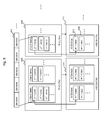
- FIG. 9 is a diagram for explaining the relationship between chunks, chunk sets, and chunk groups.
- the chunk group includes a plurality of chunk sets.
- the invalidation unit is a chunk set to which a plurality of physical blocks that are data erasure units are assigned.
- data stored in the invalidation unit is, for example, a message group in BSP graph processing.
- the size of each message is smaller than the block size.
- BSP graph processing a large number of vertices are processed at each superstep. For this reason, the number of messages output from the apex also increases.
- the non-volatile memory device 101 of this embodiment can prevent data fragmentation and reduce the number of GCs by setting an invalidation unit to which a plurality of erase units are assigned. Note that a chunk set that is an invalidation unit stores a set of messages destined for one vertex set in one super step.
- a chunk set vertical chunk
- the number of DMAs 115 buses 116
- the chunk set can be changed by the user according to the usage status.
- the user may set a part of the memory chip 111 connected to each DMA 115 (bus 116) as a chunk set, or collect a plurality of chunks 920 connected to one or a plurality of DMAs 115 (bus 116).
- a chunk set may be set.
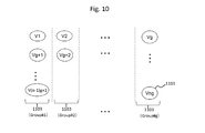
- FIG. 10 is a diagram for explaining the grouping process of the vertex 1101.
- the vertex grouping process is executed by the grouping processing unit 321.
- the grouping processing unit 321 distributes all vertices 1101 executed in each BSP graph process to the vertex group 1103.
- the vertex group 1103 is defined by the size of the working area 229 in the main memory 122 necessary for reading the vertex 1101. In other words, the total size of messages input to one vertex group in one superstep is less than or equal to the size of the working area 229.
- the host 102 determines the number of vertices belonging to the vertex group according to the vertex data read out to the working area 229 and the message size.
- a remainder value obtained by dividing the vertex ID of each vertex 1101 by the number of vertex groups (g) is set as the vertex group ID.
- the distribution method is not limited to the above method. For example, a method of assigning to vertex groups in the order of vertex IDs may be used.
- each vertex calculation processing unit 301 defines each vertex, and the calculation processing unit 312 executes processing for each vertex according to an instruction from the calculation processing order control unit 311.
- Each vertex may be processed in parallel by a plurality of CPUs 121, or may be processed in parallel by a plurality of cores in CPU 121. Further, each vertex need not be processed strictly in parallel by a plurality of CPUs 121 (or cores) as long as it is processed in batches for each super step.
- FIG. 11 is a diagram for explaining the order of processing of the vertex groups in the super step.
- the calculation processing order control unit 311 performs control so that each vertex 1101 is processed for each vertex group 1103 in the super step.
- the read size of the vertices 1101 and the message 1102 can be made smaller than the size of the working area 229 of the main memory 122. That is, the number of vertices 1101 in the vertex group 1103 can be determined so as to be equal to or smaller than the size of the working area 229.
- the calculation processing order control unit 311 stores the determined number of vertices 1101 in the working area 229 of the main memory 122.
- calculation processing order control unit 311 may determine the processing order of the vertex groups before the processing of each super step or before the execution of the graph processing. Further, the number of vertices processed in the graph processing, the number of vertices belonging to the vertex group, and the number of vertex groups may be set by the user in the user code program of the host 102.
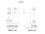
- FIG. 12 is a diagram for explaining a vertex set.
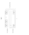
- the host 102 satisfies a preset condition, the host 102 defines a vertex set including a plurality of vertex groups 1103. For example, since one vertex group uses two chunk sets, the calculation processing order control unit 311 lacks chunk sets when the number of chunk sets is less than twice the number of vertex groups. Define. In this embodiment, a case where a vertex set is defined will be described.
- the host 102 allocates one chunk set as a storage destination of the message 1102 destined for each vertex of one vertex set.
- One vertex set may be one vertex group.
- the calculation processing order control unit 311 assigns a plurality of vertex groups to one vertex set. include.
- a read chunk set for storing a message input to one vertex set during one super step, and a message for storing a message output with each vertex of the vertex set as a destination.
- Two chunk sets can be prepared, including a built-in chunk set.
- the number of vertices included in the vertex group is set according to the size of the working area 229. For this reason, when the number of vertex groups exceeds twice the number of chunk sets, all vertex groups can be assigned to the chunk sets by defining the vertex set.
- FIG. 13 is an example of an address table.
- the host 102 has two address tables, a current address table 223 and a previous address table 224.
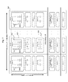
- the current address table 223 is a logical page that stores messages 1102 that are processed and output by each vertex group 401 in the super step (current super step) being executed and the vertex 1101 in each vertex group 1103 in the BSP graph processing.
- 10 is a table for associating an address list 402 that is a list of logical addresses of 922; For example, in the address list 402, a logical address indicating the logical page 922 included in the chunk set assigned to each vertex group 1103 is set.
- the previous address table 224 is processed at the vertex group 1103 that is the destination of the message that is output in the super step immediately before the current super step (previous super step), and each vertex 1101 in each vertex group 1103. 3 is a table that associates the logical address of the message 1102 to be processed.
- These address tables 222 and 223 have the same configuration. Hereinafter, a common configuration of these address tables will be described.
- the address table has an entry for each vertex group 1103. Each entry has a Group ID 401 that identifies the vertex group 1103 and an address list 402 that is a list of logical addresses of the logical page 922 in which a message 1102 destined for each vertex 1101 in the vertex group 1103 is stored.
- FIG. 14 is an example of the chunk set allocation table 225.
- the chunk set allocation table 225 is a table that associates a vertex set composed of a plurality of vertex groups with a chunk set composed of a plurality of chunks.
- the chunk set allocation table 225 has an entry for each vertex set. Each entry has a vertex set number (#) 501 that is an identifier of the vertex set and a chunk set number (#) 502 that is an identifier of the chunk set.
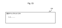
- FIG. 15 is an example of the empty chunk set list 226.
- the free chunk set list 226 is a list of chunk sets that are not assigned to the vertex set.
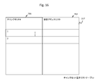
- FIG. 16 is an example of the chunk set empty list table 227.
- the chunk set empty list table 227 is a table that associates a chunk set with a logical address of a logical page 922 in the chunk set.
- the chunk set empty list table 227 has an entry for each chunk set. Each entry has a chunk set number (#) 701 that is an identifier of the chunk set, and a free address list 702 that is a list of logical addresses indicating logical pages that are not allocated to any chunk set.
- # chunk set number
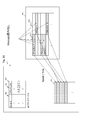
- FIG. 17 is a diagram for explaining grouping processing and writing processing of the message 1102.
- the grouping process and the writing process for the message 1102 are executed by the writing processing unit 314.
- a message 1102 input / output during the processing of the vertex 1101 includes a destination vertex ID for identifying a destination vertex (destination vertex).
- the writing processing unit 314 calculates a group ID and a local vertex ID in the group from the destination vertex ID included in the message. For example, the write processing unit 314 calculates the group ID and the local vertex ID by dividing the destination vertex ID by the number of vertex groups.
- the method for calculating the group ID and the local vertex ID from the destination vertex ID is not limited to the method described above.
- the main memory 122 has a buffer 1502 for storing the message 1102 of the vertex group 1103.
- the buffer 1502 is provided in the working area 229 of the main memory 122.
- a buffer 1502 is provided for each vertex group indicated by the group ID.
- Gr. 2 is the group ID of the vertex group.
- the write processing unit 314 stores the message 1102 in the buffer 1502 specified by the calculated group ID.
- the write processing unit 314 executes a write process.
- the writing processing unit 314 transmits the message 1102 in the buffer 1502 to the nonvolatile memory device 101.
- the write processing unit 314 refers to the current address table 223, and issues a write instruction specifying a logical address included in the address list 402 corresponding to the calculated group ID 401 to the nonvolatile memory device 101.
- the controller 112 of the nonvolatile memory device 101 refers to the chunk information and stores the message 1102 in the physical page corresponding to the logical page indicated by the designated logical address.
- the write processing unit 314 empties the contents of the buffer 1502 that has written.
- the previous address table 224 is a table for reading a message for the destination vertex.
- the message 1102 can be collected for each destination vertex group by the message grouping process.
- each address table 223 is associated with a vertex group 1103 and a logical address indicating a logical page in the corresponding chunk set. Therefore, the message 1102 destined for each vertex in the vertex group 1103 can be stored in the chunk set assigned to the vertex set including the vertex group 1103. As a result, the vertex set messages can be collectively stored in the chunk set which is the invalidation unit.
- FIG. 18 is a diagram for explaining the message 1102 reading process.
- the message reading process is executed by the reading processing unit 315.
- the read processing unit 315 reads a message necessary for executing the vertex to the working area 229 of the main memory 122. Specifically, for example, the read processing unit 315 refers to the previous address table 224 and acquires a logical address corresponding to the vertex group 1103.
- the read processing unit 315 transmits a read command specifying the acquired logical address to the nonvolatile memory device 101. For example, when reading the message 1102 necessary for executing each vertex 1101 of the vertex group # 2 to the main memory 122, the read processing unit 315 refers to the previous address table 224 and sends a read command designating the logical addresses A to E. Transmit to the non-volatile memory device 101.
- the calculation processing order control unit 311 refers to the all address table 224 and sets logical addresses corresponding to all the vertex groups 1103 included in the vertex set.
- the designated trim command is transmitted to the nonvolatile memory device 101.
- the trim command is a command for notifying a logical address in which unnecessary data is stored.
- the host 102 of this embodiment notifies the non-volatile memory device 101 of a logical address of a message that is no longer necessary for each vertex set in one super step by a trim command.
- the controller 112 that has received the read command reads out the message 1102 stored in the physical page corresponding to the designated logical address based on the chunk information and transmits it to the host 102. Then, the controller 112 that has received the trim command cancels the allocation of the designated logical address to the target physical page, and invalidates the target physical page.
- messages 1102 necessary for the processing of the vertices of the vertex group 1103 can be collectively read.
- the physical page in which the read message 1102 is stored can be invalidated for each chunk set corresponding to the vertex set.
- messages used by one vertex set are collectively stored in one chunk set. For this reason, messages in one chunk set are invalidated together. Therefore, the number of GC can be reduced.
- the writing processing unit 314 discards the contents of the previous address table 224 and copies the contents of the current address table 223 to the previous address table 224.
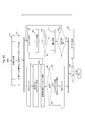
- FIG. 19 illustrates a flowchart of the write range control process according to the present embodiment.
- This process is a process executed by the host 102 when the BSP graph process starts.
- initial data including the vertex 1101 necessary for the BSP graph processing is stored in a storage device (not shown) (for example, SSD, HDD; Hard disk drive, etc.) different from the nonvolatile memory device 101.
- the calculation processing order control unit 311 executes initialization processing (S901). Details of the initialization process will be described later.
- initialization processing a logical address range used for the BSP graph process is set, and the chunk group 960 that can be used and the number of chunk sets in the chunk group 960 are calculated based on this logical address range. Then, the logical address range of the chunk set is assigned to the vertex set, and the chunk set assignment table 225 is generated.
- the calculation processing order control unit 311 stores the initial data, which is the initial value of each vertex used for the BSP graph processing, in one or more chunk sets, and updates the free chunk set list 226 (S902). For example, the calculation processing order control unit 311 calculates the logical address of the logical page corresponding to each chunk set, and transmits a read command designating the logical address to the nonvolatile memory device 101. In this case, for example, the calculation processing order control unit 311 may collect initial data for each vertex group 1103 and store them in a chunk set.
- the controller 112 of the nonvolatile memory 101 receives the initial data and stores the initial data in the physical page 933 corresponding to the chunk set.
- the calculation processing order control unit 311 repeats the vertex group processing (S903 to S906).
- the vertex group process will be described below.
- a vertex group that is a target of vertex group processing is referred to as a target vertex group.
- the calculation processing order control unit 311 refers to the previous address table 224 and executes a reading process of reading a message having each vertex of the target vertex group as a destination vertex to the main memory 122 (S903).
- the reading process is as described in FIG. Specifically, for example, the calculation processing order control unit 311 refers to the previous address table 224 and acquires a logical address included in the address list 402 corresponding to the vertex group ID 401 of the target vertex group. Then, the calculation processing order control unit 311 transmits a read command specifying the acquired logical address to the nonvolatile memory device 101.
- the calculation processing order control unit 311 adds the acquired logical address to the free address list 702 of the chunk set free list table 227.
- controller 112 of the non-volatile memory device 101 transmits the message 1102 stored in the physical page corresponding to the logical address specified by the read command based on the chunk information to the host 102 by the reading process.
- the calculation processing order control unit 311 receives the message 1102 and stores the received message 1102 in the main memory 122.
- the calculation processing order control unit 311 hands over the processing to the calculation processing unit 312.
- the calculation processing unit 312 executes processing for the vertex 1101 (S904).
- the calculation processing unit 312 delivers the message 1102 generated by executing the processing of each vertex 1101 to the data communication processing unit 313.
- the data communication processing unit 313 delivers the message 1102 to the writing processing unit 314 (to S911).
- the calculation processing order control unit 311 determines whether or not the target vertex group is the last group to execute this processing in the vertex set (S905). When it is not the last vertex group (S905; No), the calculation processing order control unit 311 returns the processing to S903.
- the calculation processing order control unit 311 refers to the previous address table 224, and for each vertex group from the address list 402 corresponding to the vertex group ID 401 of each target vertex group in S903. The logical address in which the message 1102 read out is stored is acquired. Then, the calculation processing order control unit 311 transmits a trim command specifying the acquired logical address to the nonvolatile memory device 101. The calculation processing order control unit 311 adds the acquired chunk set number (#) to the free chunk set list 226, and advances the processing to S907.
- the controller 112 invalidates the physical page corresponding to the logical address specified by the trim command.
- the write processing unit 314 receives a message from the calculation processing order control unit 311 via the data communication processing unit 313 (S911).
- the write processing unit 314 executes a message grouping process for grouping the received message 1102 for each destination vertex (S912).
- the grouping process is as described with reference to FIG.
- a message with the vertex group vertex as the destination is stored in the buffer 1502 for each vertex group.
- the write processing unit 314 determines whether or not there is a buffer area 1502 filled with the message 1102 in the working area 229 (buffer full) (S913). When there is a buffer area 1502 that is filled with the message 1102 (S913; Yes), the write processing unit 314 performs a write process (S914) and advances the process to S915.
- the outline of the writing process is as described in FIG. Details of the writing process will be described later.
- the write processing unit 314 advances the process to S915.
- the writing processing unit 314 determines whether or not the super step is completed (S915). If the super step has not ended (S915; No), the write processing unit 314 returns the process to S911. On the other hand, when the super step is finished (S915; Yes), the writing processing unit 314 notifies the calculation processing order control unit 311 that the super step is finished, and waits.
- calculation processing order control unit 311 When the calculation processing order control unit 311 receives the notification from the writing processing unit 314 and completes the vertex group processing of the plurality of vertex groups 1103 in the vertex set, the calculation processing sequence control unit 311 advances the processing to S907.
- the calculation processing order control unit 311 determines whether or not the BSP graph processing is finished (S907). When it is determined that the BSP graph processing has not ended (S907; No), the calculation processing order control unit 311 updates the chunk set allocation table 225 so as to deallocate the chunk set and the vertex group (S908), and the previous address The information in the table 224 is discarded, the data in the current address table 223 is copied to the previous address table 224, and the process returns to S903. Thereby, the next super step is started.
- a physical block in which a message group destined for each vertex set is stored by storing unnecessary messages after being used for vertex processing in a chunk set for each vertex set. Can be limited. Thereby, even when a very large number of vertex processes are executed, such as a BSP graph process, frequent occurrence of GC in the nonvolatile memory device 101 can be prevented. Accordingly, it is possible to prevent a decrease in the lifetime of the nonvolatile memory and a decrease in the access performance of the nonvolatile memory.
- the message 1102 becomes unnecessary when the processing of the vertex 1101 of the destination (input destination) of the message 1102 is completed.
- the vertex set By setting the vertex set, messages 1102 that become unnecessary at a certain timing can be collectively stored in the same chunk set.
- an invalidation instruction (trim command) is transmitted to the nonvolatile memory device 101, whereby the physical block assigned to the chunk set corresponding to the vertex set is transmitted. Can be erased together. Therefore, fragmentation of data in the physical block can be prevented, the number of GCs can be reduced, and a decrease in the lifetime of the nonvolatile memory can be prevented.
- the chunk set by configuring the chunk set with a plurality of chunks based on the hardware configuration, for example, with a plurality of chunks corresponding to the memory chips 111 respectively connected to all the buses in the nonvolatile memory device 101 one by one.
- the access performance of the host 102 to the nonvolatile memory device 101 can be improved.
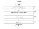
- FIG. 20 is a flowchart of the initialization process.
- the initialization process is the process of S901 in the writing range control process.
- the address range of the non-volatile memory device 101 that the user wants to use in the BSP graph processing is specified via the user code program 221, and the management middleware uses the logical address range (logical address size or start logical address-end logical address). ) Is determined, the calculation processing order control unit 311 of the framework program 222 is activated (S801).
- the calculation processing order control unit 311 determines a chunk group 960 as a range of chunks 920 that can be used for BSP graph processing based on the determined logical address range and the chunk information received from the nonvolatile memory device 101 (S802). .
- the calculation processing order control unit 311 may use the chunk group number of the chunk group 960, the chunk number (vertical chunk number and horizontal chunk number) of each chunk 920 in the chunk group 960, the number of chunks in the chunk group 960, and the like. May be calculated.
- the calculation processing order control unit 311 may generate and store logical-physical conversion information that associates the logical page in the chunk with the physical page in the memory chip based on the chunk information.
- the calculation processing order control unit 311 calculates the number of chunk sets based on the calculation result and chunk information in S802 (S803). For example, the calculation processing order control unit 311 calculates a value obtained by dividing the number of chunks in the chunk group 960 by the number of horizontal chunks (the number of DMAs in the nonvolatile memory device 101) as the number of chunk sets.
- the calculation processing order control unit 311 determines the number of vertex sets according to the number of chunk sets (S804). The method for calculating the number of vertex sets is as described with reference to FIG. The calculation processing order control unit 311 creates the determined number of vertex sets.
- the host 102 can calculate the number of chunk sets and the like based on the chunk information transmitted from the nonvolatile memory device 101, and generate a vertex set corresponding to each chunk set.
- FIG. 21 is a flowchart of the writing process.
- the writing process is the process of S914 in the writing range control process.
- the vertex group to be written is referred to as a writing vertex group.
- the write processing unit 314 calculates the vertex set ID of the vertex set (write vertex set) to which the write vertex group belongs from the vertex group ID of the write vertex group (S1002).
- the write processing unit 314 refers to the chunk set allocation table 225, (a) a chunk set (write chunk set) corresponding to the write vertex set is set, and (b) an empty address in the write chunk set It is determined whether or not exists. In the case of (a) and (b), the writing processing unit 314 advances the processing to S1007. On the other hand, if the write processing unit 314 does not satisfy at least one of the requirements (a) and (b), the process proceeds to S1004.
- the write processing unit 314 refers to the free chunk set list 226 and determines whether there is a free chunk set (S1004). If there is an empty chunk set (S1004; Yes), any empty chunk set is set in the writing vertex set, and the chunk set allocation table is updated (S1006). Then, the writing processing unit 314 advances the processing to S1007.
- the writing processing unit 314 refers to the chunk set allocation table 225 and the chunk set empty table 227, and sets a vertex set different from the vertex set of the writing vertex set.
- a chunk set that is a corresponding chunk set and has a free address is acquired (S1005).
- the writing processing unit 314 may acquire a chunk set corresponding to a vertex set having an ID close to the ID of the writing vertex set.
- the writing processing unit 314 sets the acquired chunk set as the writing vertex set (S1006), and advances the processing to S1007.
- the write processing unit 314 refers to the chunk set free list table 227, acquires a free address (logical address) corresponding to the set chunk set, and updates the free address list (S1007). Specifically, the write processing unit 314 deletes the acquired logical address from the free address list 226.
- the write processing unit 314 transmits a logical address corresponding to a message addressed to each vertex of the write vertex group to the nonvolatile memory device 101 (S1008).
- the controller 112 of the nonvolatile memory device 101 receives the logical address, and stores the message in the physical page corresponding to the received logical address based on the chunk information.
- a message can be stored in the chunk set assigned to the vertex set to which the writing vertex group belongs (writing vertex set).
- the vertex A write vertex set can be assigned to another free chunk set to which no set is assigned, and a message can be stored in that chunk set.
- the host 102 assigns one chunk set to one vertex set, and in one super step, a plurality of vertex groups in one vertex set are destined, and an input message is sent to one chunk set. Write to.
- the host 102 assigns one chunk set to one vertex set, and in one super step, a plurality of vertex groups in one vertex set are destined, and an input message is sent to one chunk set. Write to.
- it is not limited to this mode.
- the host 102 may assign one chunk to one vertex group and write a message 1102 input with one vertex group 1103 as the destination in one superstep to one chunk 920.
- the host 102 specifies a chunk number corresponding to the vertex group number using the chunk information, and writes a message in the logical address range corresponding to the chunk number.
- the write range control process can be executed in smaller units.
- the storage device corresponds to the nonvolatile memory device 101
- the processor corresponds to the CPU 121
- the storage device corresponds to the main memory 122.
- the first limited logical area and the second limited logical area correspond to different chunk sets or different chunks.
- the limited information corresponds to chunk information
- the specific command corresponds to a trim command.
- the processing data corresponds to the message.
- the limited logical area information corresponds to the chunk set allocation table 225, the empty chunk set list 226, the chunk set empty list table 227, and the like.
Landscapes
- Engineering & Computer Science (AREA)
- Theoretical Computer Science (AREA)
- Physics & Mathematics (AREA)
- General Engineering & Computer Science (AREA)
- General Physics & Mathematics (AREA)
- Human Computer Interaction (AREA)
- Techniques For Improving Reliability Of Storages (AREA)
Abstract
Selon l'invention, un dispositif de stockage stocke des informations de limitation concernant la taille d'une première zone logique limitée, qui est une partie d'une zone de stockage logique d'une mémoire non volatile, associe une première zone de stockage physique, qui est une partie d'une zone de stockage physique de la mémoire non volatile, avec la première zone logique limitée d'après les informations de limitation, et transmet les informations de limitation à un ordinateur hôte. L'ordinateur hôte exécute un premier processus, ce qui permet de générer des premières données traitées. L'ordinateur hôte calcule une plage de premières adresses logiques indiquant la première zone logique limitée, d'après les informations de limitation, et transmet, au dispositif de stockage, les premières données traitées et une première commande d'écriture spécifiant une première adresse logique particulière dans la plage de premières adresses logiques. Au terme du premier processus, l'ordinateur hôte transmet une commande de lecture spécifiant la première adresse logique particulière au dispositif de stockage, et transmet également, au dispositif de stockage, une commande spécifique indiquant que la plage de premières adresses logiques n'est plus nécessaire.
Priority Applications (1)
| Application Number | Priority Date | Filing Date | Title |
|---|---|---|---|
| PCT/JP2015/058100 WO2016147351A1 (fr) | 2015-03-18 | 2015-03-18 | Système informatique, procédé et ordinateur hôte |
Applications Claiming Priority (1)
| Application Number | Priority Date | Filing Date | Title |
|---|---|---|---|
| PCT/JP2015/058100 WO2016147351A1 (fr) | 2015-03-18 | 2015-03-18 | Système informatique, procédé et ordinateur hôte |
Publications (1)
| Publication Number | Publication Date |
|---|---|
| WO2016147351A1 true WO2016147351A1 (fr) | 2016-09-22 |
Family
ID=56918477
Family Applications (1)
| Application Number | Title | Priority Date | Filing Date |
|---|---|---|---|
| PCT/JP2015/058100 Ceased WO2016147351A1 (fr) | 2015-03-18 | 2015-03-18 | Système informatique, procédé et ordinateur hôte |
Country Status (1)
| Country | Link |
|---|---|
| WO (1) | WO2016147351A1 (fr) |
Citations (3)
| Publication number | Priority date | Publication date | Assignee | Title |
|---|---|---|---|---|
| US6763519B1 (en) * | 1999-05-05 | 2004-07-13 | Sychron Inc. | Multiprogrammed multiprocessor system with lobally controlled communication and signature controlled scheduling |
| WO2014196055A1 (fr) * | 2013-06-06 | 2014-12-11 | 株式会社日立製作所 | Système de traitement d'informations et procédé de traitement de données |
| WO2015008358A1 (fr) * | 2013-07-18 | 2015-01-22 | 株式会社日立製作所 | Dispositif de traitement d'informations |
-
2015
- 2015-03-18 WO PCT/JP2015/058100 patent/WO2016147351A1/fr not_active Ceased
Patent Citations (3)
| Publication number | Priority date | Publication date | Assignee | Title |
|---|---|---|---|---|
| US6763519B1 (en) * | 1999-05-05 | 2004-07-13 | Sychron Inc. | Multiprogrammed multiprocessor system with lobally controlled communication and signature controlled scheduling |
| WO2014196055A1 (fr) * | 2013-06-06 | 2014-12-11 | 株式会社日立製作所 | Système de traitement d'informations et procédé de traitement de données |
| WO2015008358A1 (fr) * | 2013-07-18 | 2015-01-22 | 株式会社日立製作所 | Dispositif de traitement d'informations |
Non-Patent Citations (1)
| Title |
|---|
| CHEN CHEN ET AL.: "The Application of the BSP Model on DataGrid", SERVICES COMPUTING, 2004 (SCC 2004), PROCEEDINGS OF THE 2004 IEEE INTERNATIONAL CONFERENCE ON, 15 September 2004 (2004-09-15), pages 471 - 474, XP010741563, DOI: doi:10.1109/SCC.2004.1358045 * |
Similar Documents
| Publication | Publication Date | Title |
|---|---|---|
| JP7353934B2 (ja) | メモリシステムおよび制御方法 | |
| JP7366795B2 (ja) | メモリシステムおよび制御方法 | |
| TWI682278B (zh) | 記憶體系統及控制方法 | |
| CN109240938B (zh) | 存储系统以及控制非易失性存储器的控制方法 | |
| CN114115747B (zh) | 存储器系统及控制方法 | |
| JP6524039B2 (ja) | メモリシステム及び制御方法 | |
| JP6403164B2 (ja) | メモリシステム | |
| US10102118B2 (en) | Memory system and non-transitory computer readable recording medium | |
| JP6007332B2 (ja) | ストレージシステム及びデータライト方法 | |
| TW201917580A (zh) | 計算機系統及儲存裝置之控制方法 | |
| JP6455900B2 (ja) | ストレージシステムおよびシステムガベージコレクション方法 | |
| CN111309648A (zh) | 存储装置及其操作方法 | |
| JP2022171208A (ja) | メモリシステムおよび制御方法 | |
| JP2023012773A (ja) | メモリシステムおよび制御方法 | |
| CN111198825B (zh) | 存储设备和包括存储设备的存储系统 | |
| JP4745465B1 (ja) | 半導体記憶装置及び半導体記憶装置の制御方法 | |
| CN114185480A (zh) | 存储器系统和数据处理系统 | |
| KR20180126656A (ko) | 데이터 저장 장치 및 그것의 동작 방법 | |
| TWI895988B (zh) | 記憶體系統及控制方法 | |
| JP2019212103A (ja) | メモリシステム | |
| US12072797B2 (en) | Memory system and non-transitory computer readable recording medium | |
| CN103489482A (zh) | 信息处理设备、方法和程序 | |
| US12517819B2 (en) | Fast LBA/PBA table rebuild by skipping read of metadata of LBA bin that is not mapped | |
| WO2016147351A1 (fr) | Système informatique, procédé et ordinateur hôte | |
| JP6652605B2 (ja) | メモリシステムの制御方法 |
Legal Events
| Date | Code | Title | Description |
|---|---|---|---|
| 121 | Ep: the epo has been informed by wipo that ep was designated in this application |
Ref document number: 15885447 Country of ref document: EP Kind code of ref document: A1 |
|
| NENP | Non-entry into the national phase |
Ref country code: DE |
|
| 122 | Ep: pct application non-entry in european phase |
Ref document number: 15885447 Country of ref document: EP Kind code of ref document: A1 |
|
| NENP | Non-entry into the national phase |
Ref country code: JP |