WO2016148087A1 - Dispositif d'éclairage et dispositif d'affichage - Google Patents
Dispositif d'éclairage et dispositif d'affichage Download PDFInfo
- Publication number
- WO2016148087A1 WO2016148087A1 PCT/JP2016/057858 JP2016057858W WO2016148087A1 WO 2016148087 A1 WO2016148087 A1 WO 2016148087A1 JP 2016057858 W JP2016057858 W JP 2016057858W WO 2016148087 A1 WO2016148087 A1 WO 2016148087A1
- Authority
- WO
- WIPO (PCT)
- Prior art keywords
- light source
- power supply
- connector
- bottom wall
- light
- Prior art date
- Legal status (The legal status is an assumption and is not a legal conclusion. Google has not performed a legal analysis and makes no representation as to the accuracy of the status listed.)
- Ceased
Links
Images




Classifications
-
- G—PHYSICS
- G02—OPTICS
- G02B—OPTICAL ELEMENTS, SYSTEMS OR APPARATUS
- G02B6/00—Light guides; Structural details of arrangements comprising light guides and other optical elements, e.g. couplings
- G02B6/0001—Light guides; Structural details of arrangements comprising light guides and other optical elements, e.g. couplings specially adapted for lighting devices or systems
- G02B6/0011—Light guides; Structural details of arrangements comprising light guides and other optical elements, e.g. couplings specially adapted for lighting devices or systems the light guides being planar or of plate-like form
- G02B6/0033—Means for improving the coupling-out of light from the light guide
- G02B6/005—Means for improving the coupling-out of light from the light guide provided by one optical element, or plurality thereof, placed on the light output side of the light guide
- G02B6/0055—Reflecting element, sheet or layer
-
- G—PHYSICS
- G02—OPTICS
- G02F—OPTICAL DEVICES OR ARRANGEMENTS FOR THE CONTROL OF LIGHT BY MODIFICATION OF THE OPTICAL PROPERTIES OF THE MEDIA OF THE ELEMENTS INVOLVED THEREIN; NON-LINEAR OPTICS; FREQUENCY-CHANGING OF LIGHT; OPTICAL LOGIC ELEMENTS; OPTICAL ANALOGUE/DIGITAL CONVERTERS
- G02F1/00—Devices or arrangements for the control of the intensity, colour, phase, polarisation or direction of light arriving from an independent light source, e.g. switching, gating or modulating; Non-linear optics
- G02F1/01—Devices or arrangements for the control of the intensity, colour, phase, polarisation or direction of light arriving from an independent light source, e.g. switching, gating or modulating; Non-linear optics for the control of the intensity, phase, polarisation or colour
- G02F1/13—Devices or arrangements for the control of the intensity, colour, phase, polarisation or direction of light arriving from an independent light source, e.g. switching, gating or modulating; Non-linear optics for the control of the intensity, phase, polarisation or colour based on liquid crystals, e.g. single liquid crystal display cells
- G02F1/133—Constructional arrangements; Operation of liquid crystal cells; Circuit arrangements
- G02F1/1333—Constructional arrangements; Manufacturing methods
- G02F1/1335—Structural association of cells with optical devices, e.g. polarisers or reflectors
- G02F1/1336—Illuminating devices
- G02F1/133602—Direct backlight
- G02F1/133603—Direct backlight with LEDs
-
- F—MECHANICAL ENGINEERING; LIGHTING; HEATING; WEAPONS; BLASTING
- F21—LIGHTING
- F21S—NON-PORTABLE LIGHTING DEVICES; SYSTEMS THEREOF; VEHICLE LIGHTING DEVICES SPECIALLY ADAPTED FOR VEHICLE EXTERIORS
- F21S2/00—Systems of lighting devices, not provided for in main groups F21S4/00 - F21S10/00 or F21S19/00, e.g. of modular construction
-
- F—MECHANICAL ENGINEERING; LIGHTING; HEATING; WEAPONS; BLASTING
- F21—LIGHTING
- F21V—FUNCTIONAL FEATURES OR DETAILS OF LIGHTING DEVICES OR SYSTEMS THEREOF; STRUCTURAL COMBINATIONS OF LIGHTING DEVICES WITH OTHER ARTICLES, NOT OTHERWISE PROVIDED FOR
- F21V23/00—Arrangement of electric circuit elements in or on lighting devices
-
- F—MECHANICAL ENGINEERING; LIGHTING; HEATING; WEAPONS; BLASTING
- F21—LIGHTING
- F21V—FUNCTIONAL FEATURES OR DETAILS OF LIGHTING DEVICES OR SYSTEMS THEREOF; STRUCTURAL COMBINATIONS OF LIGHTING DEVICES WITH OTHER ARTICLES, NOT OTHERWISE PROVIDED FOR
- F21V23/00—Arrangement of electric circuit elements in or on lighting devices
- F21V23/06—Arrangement of electric circuit elements in or on lighting devices the elements being coupling devices, e.g. connectors
-
- G—PHYSICS
- G02—OPTICS
- G02F—OPTICAL DEVICES OR ARRANGEMENTS FOR THE CONTROL OF LIGHT BY MODIFICATION OF THE OPTICAL PROPERTIES OF THE MEDIA OF THE ELEMENTS INVOLVED THEREIN; NON-LINEAR OPTICS; FREQUENCY-CHANGING OF LIGHT; OPTICAL LOGIC ELEMENTS; OPTICAL ANALOGUE/DIGITAL CONVERTERS
- G02F1/00—Devices or arrangements for the control of the intensity, colour, phase, polarisation or direction of light arriving from an independent light source, e.g. switching, gating or modulating; Non-linear optics
- G02F1/01—Devices or arrangements for the control of the intensity, colour, phase, polarisation or direction of light arriving from an independent light source, e.g. switching, gating or modulating; Non-linear optics for the control of the intensity, phase, polarisation or colour
- G02F1/13—Devices or arrangements for the control of the intensity, colour, phase, polarisation or direction of light arriving from an independent light source, e.g. switching, gating or modulating; Non-linear optics for the control of the intensity, phase, polarisation or colour based on liquid crystals, e.g. single liquid crystal display cells
- G02F1/133—Constructional arrangements; Operation of liquid crystal cells; Circuit arrangements
- G02F1/1333—Constructional arrangements; Manufacturing methods
-
- G—PHYSICS
- G02—OPTICS
- G02F—OPTICAL DEVICES OR ARRANGEMENTS FOR THE CONTROL OF LIGHT BY MODIFICATION OF THE OPTICAL PROPERTIES OF THE MEDIA OF THE ELEMENTS INVOLVED THEREIN; NON-LINEAR OPTICS; FREQUENCY-CHANGING OF LIGHT; OPTICAL LOGIC ELEMENTS; OPTICAL ANALOGUE/DIGITAL CONVERTERS
- G02F1/00—Devices or arrangements for the control of the intensity, colour, phase, polarisation or direction of light arriving from an independent light source, e.g. switching, gating or modulating; Non-linear optics
- G02F1/01—Devices or arrangements for the control of the intensity, colour, phase, polarisation or direction of light arriving from an independent light source, e.g. switching, gating or modulating; Non-linear optics for the control of the intensity, phase, polarisation or colour
- G02F1/13—Devices or arrangements for the control of the intensity, colour, phase, polarisation or direction of light arriving from an independent light source, e.g. switching, gating or modulating; Non-linear optics for the control of the intensity, phase, polarisation or colour based on liquid crystals, e.g. single liquid crystal display cells
- G02F1/133—Constructional arrangements; Operation of liquid crystal cells; Circuit arrangements
- G02F1/1333—Constructional arrangements; Manufacturing methods
- G02F1/1335—Structural association of cells with optical devices, e.g. polarisers or reflectors
- G02F1/1336—Illuminating devices
- G02F1/133602—Direct backlight
- G02F1/133608—Direct backlight including particular frames or supporting means
-
- H—ELECTRICITY
- H05—ELECTRIC TECHNIQUES NOT OTHERWISE PROVIDED FOR
- H05K—PRINTED CIRCUITS; CASINGS OR CONSTRUCTIONAL DETAILS OF ELECTRIC APPARATUS; MANUFACTURE OF ASSEMBLAGES OF ELECTRICAL COMPONENTS
- H05K1/00—Printed circuits
- H05K1/02—Details
- H05K1/14—Structural association of two or more printed circuits
- H05K1/142—Arrangements of planar printed circuit boards in the same plane, e.g. auxiliary printed circuit insert mounted in a main printed circuit
-
- G—PHYSICS
- G02—OPTICS
- G02F—OPTICAL DEVICES OR ARRANGEMENTS FOR THE CONTROL OF LIGHT BY MODIFICATION OF THE OPTICAL PROPERTIES OF THE MEDIA OF THE ELEMENTS INVOLVED THEREIN; NON-LINEAR OPTICS; FREQUENCY-CHANGING OF LIGHT; OPTICAL LOGIC ELEMENTS; OPTICAL ANALOGUE/DIGITAL CONVERTERS
- G02F1/00—Devices or arrangements for the control of the intensity, colour, phase, polarisation or direction of light arriving from an independent light source, e.g. switching, gating or modulating; Non-linear optics
- G02F1/01—Devices or arrangements for the control of the intensity, colour, phase, polarisation or direction of light arriving from an independent light source, e.g. switching, gating or modulating; Non-linear optics for the control of the intensity, phase, polarisation or colour
- G02F1/13—Devices or arrangements for the control of the intensity, colour, phase, polarisation or direction of light arriving from an independent light source, e.g. switching, gating or modulating; Non-linear optics for the control of the intensity, phase, polarisation or colour based on liquid crystals, e.g. single liquid crystal display cells
- G02F1/133—Constructional arrangements; Operation of liquid crystal cells; Circuit arrangements
- G02F1/1333—Constructional arrangements; Manufacturing methods
- G02F1/1335—Structural association of cells with optical devices, e.g. polarisers or reflectors
- G02F1/1336—Illuminating devices
- G02F1/133602—Direct backlight
- G02F1/133612—Electrical details
-
- H—ELECTRICITY
- H05—ELECTRIC TECHNIQUES NOT OTHERWISE PROVIDED FOR
- H05K—PRINTED CIRCUITS; CASINGS OR CONSTRUCTIONAL DETAILS OF ELECTRIC APPARATUS; MANUFACTURE OF ASSEMBLAGES OF ELECTRICAL COMPONENTS
- H05K2201/00—Indexing scheme relating to printed circuits covered by H05K1/00
- H05K2201/10—Details of components or other objects attached to or integrated in a printed circuit board
- H05K2201/10007—Types of components
- H05K2201/10106—Light emitting diode [LED]
Definitions
- the present invention relates to an illumination device and a display device in which a plurality of light source substrates are juxtaposed.
- the liquid crystal display device includes a liquid crystal display panel and an illumination device having a plurality of LEDs (light emitting diodes).
- the illumination device illuminates the liquid crystal display panel from the back side.
- an edge light type lighting device a plurality of LEDs are juxtaposed facing the end face of a light guide plate disposed facing the liquid crystal display panel (see Patent Document 1).
- a plurality of LEDs are juxtaposed facing the back surface of the liquid crystal display panel (see Patent Documents 2 to 4).
- the direct type is more advantageous than the edge light type.
- the direct type illumination device will be described.
- the LED is mounted on an LED substrate and accommodated in a dish-shaped chassis.
- the LED substrate is fixed to the bottom wall of the chassis.
- a power supply circuit for supplying power to the LEDs is disposed outside the chassis.
- a single rectangular LED substrate having a large aspect ratio and a large area is disposed, and a plurality of strip-shaped LED substrates having a small aspect ratio and a small area are juxtaposed. Compare with the case.
- the power supply circuit and one LED substrate need only be connected by a small number of power supply lines, and wiring is easy.
- the power supply circuit and each of the plurality of LED substrates must be connected by a large number of power supply lines, so that wiring is difficult.
- the present invention has been made in view of such circumstances, and a main object thereof is to provide an illumination device and a display device that can be easily wired.
- the lighting device includes a dish-shaped container, a light source mounted on one surface of each, a plurality of light source substrates juxtaposed on the inner surface of the bottom wall of the container, the one surface, and the container
- a lighting device including a reflection sheet that covers an inner surface of the body and reflects light, and a power supply unit, a connector provided on the one surface and a flexible printed circuit board are used, and the gap is formed between the bottom wall and the reflection sheet.
- a power supply member for supplying power from the power supply unit to the light source board, and a light source connection unit provided on the power supply member and electrically connected to the connector.
- the power supply member has a strip shape and is electrically connected to the power supply unit
- the light source substrate has a strip shape
- the light source substrate along the length direction of the power supply member It is characterized by being juxtaposed in the width direction.
- the power supply member has a belt shape and is electrically connected to the power supply unit, and ends of the two light source substrates are adjacent to each other in the width direction of the power supply member,
- the connector is arranged at the end portion.
- the light source includes a light emitting unit mounted on the one surface, a light incident unit that covers the light emitting unit and receives light emitted from the light emitting unit, and light incident on the light incident unit.
- the height of the part covering the one surface of the reflection sheet from the one surface is lower than the height from the one surface of the light emitting unit.
- a through hole is provided in the bottom wall, and the power supply unit is disposed on an outer surface of the bottom wall, and is electrically connected to the power feeding member through the through hole. It is characterized by.
- the illuminating device is characterized in that the light source connecting portion and a power source connecting portion for electrical connection with the power source portion are provided on one surface of the power supply member.
- the portion of the power supply member provided with the light source connection portion covers the connector, the power supply member has a tongue-shaped piece, and the tongue-shaped piece is the bottom wall. It is characterized in that it is closely fixed to.
- the power supply member includes a belt-like main body portion and a plurality of arm-shaped pieces projecting from the main body portion, and the light source connection portion is provided on the arm-shaped piece. It is characterized by being.
- the lighting device according to the present invention is characterized in that each light source substrate and the power supply unit are individually electrically connected via the power feeding member.
- the lighting device includes a dish-shaped container, a light source mounted on one surface of each, a plurality of light source substrates juxtaposed on the inner surface of the bottom wall of the container, the one surface, and the container
- a lighting device including a reflection sheet that covers an inner surface of a body and reflects light, and a power supply unit
- the light source substrate has a strip shape, and is a connector provided on the one surface at a non-end portion in the length direction of the light source substrate.
- a flexible printed circuit board or a flat cable and is arranged between the bottom wall and the reflection sheet, and is provided on the power supply member for supplying power from the power supply unit to the light source substrate.
- a light source connecting portion electrically connected to the connector.
- the illuminating device according to the present invention is characterized in that the connector is disposed in two central regions obtained by virtually dividing the light source substrate into four equal parts in the length direction.
- the illuminating device according to the present invention is characterized in that the connector is disposed at an end in a width direction of the light source substrate.
- At least one of the light source substrates is disposed on a peripheral portion of the bottom wall, and the power supply member is located on the bottom of the light source substrate disposed on the peripheral portion of the bottom wall. It is arranged on the center side of the wall.
- the illuminating device according to the present invention is characterized in that the light source substrate or the power feeding member is fastened together with the bottom wall together with the reflection sheet.
- a display device includes the illumination device according to the present invention and a display panel illuminated from the back side by the illumination device.
- a television receiver includes a display device according to the present invention and a receiving unit that receives a television broadcast, and displays video on the display device based on the television broadcast received by the receiving unit. It is characterized by being.
- wiring between the power supply unit and the light source substrate can be easily performed using a flexible printed circuit board.
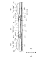
- FIG. 1 It is sectional drawing which shows schematically the structure of a television receiver provided with the display apparatus which concerns on Embodiment 1 of this invention. It is a front view which briefly shows the structure of the illuminating device with which a display apparatus is provided. It is an enlarged front view which outlines the structure of an illuminating device. It is sectional drawing which shows schematically the structure of the light source board
- FIG. 1 is a cross-sectional view schematically showing a configuration of a television receiver 1 including a display device 13 according to Embodiment 1 of the present invention.
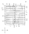
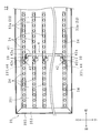
- 2 and 3 are a front view and an enlarged front view schematically showing the configuration of the illumination device 22 included in the display device 13.
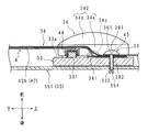
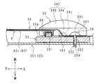
- FIG. 4 is a cross-sectional view schematically showing a configuration in the vicinity of the light source substrate 33 of the illumination device 22.
- the television receiver 1 is a stationary type or a wall-mounted type.
- the television receiver 1 includes a receiving unit 11, a signal processing unit 12, and a display device 13.
- the receiving unit 11 is a circuit board on which a not-shown receiving circuit is mounted.
- the receiving circuit receives a television broadcast from the outside via an antenna (not shown) and outputs a broadcast signal based on the received television broadcast.
- the signal processing unit 12 is a circuit board on which a signal processing circuit (not shown) is mounted.
- the signal processing circuit outputs video data by performing predetermined signal processing on the broadcast signal output from the receiving unit 11.
- the display device 13 has a rectangular shape in front view.
- the display device 13 includes a display panel 21 and a lighting device 22 and a cabinet (not shown) that houses them.
- the cabinet also houses a receiving unit 11 and a signal processing unit 12.
- the receiving unit 11 and the signal processing unit 12 may be externally attached to the display device 13.
- the display panel 21 is a rectangular plate-shaped liquid crystal display panel.
- the display panel 21 includes a rectangular display area and a rectangular frame-shaped frame area surrounding the display area.
- the display area (and the frame area) is located at the center (and peripheral edge) of the display panel 21.
- an image based on the image data output from the signal processing unit 12 is displayed.
- the illumination device 22 includes an optical sheet group 30, a diffusion plate 31, a spacer 32, a plurality of light source substrates 33, 33,..., A plurality of light sources 34, 34,.
- Two wiring members 38, 38, a plurality of co-fastening members 39, 39,..., And two power feeding members 4, 4 are provided.
- the optical sheet group 30 is formed by laminating a plurality of optical sheets each having optical transparency. Each optical sheet has a light diffusing function, a light collecting function, a polarizing function, or the like.
- the optical sheet group 30 has a rectangular shape with a larger area than the display area of the display panel 21.
- the optical sheet group 30 is disposed facing the rear surface of the display area of the display panel 21 with an appropriate distance.
- the diffusion plate 31 has light diffusibility.
- the light transmittance of the diffusion plate 31 is about 50%. A part of the light incident on the rear surface of the diffusion plate 31 is transmitted through the diffusion plate 31, diffused from the front surface of the diffusion plate 31, and emitted. Another part of the light incident on the rear surface of the diffusion plate 31 is reflected to the back side.
- the diffusion plate 31 has a rectangular shape with a larger area than the optical sheet group 30.
- the diffusing plate 31 is disposed facing the rear surface of the optical sheet group 30 with an appropriate distance.
- the spacer 32 has a frame shape and has a buffering property.
- the spacer 32 is interposed between the rear peripheral edge of the optical sheet group 30 and the front peripheral edge of the diffusion plate 31.
- the arrangement position of the spacer 32 is a position facing the frame area of the display panel 21. 2 and 3, illustration of the optical sheet group 30, the diffusion plate 31, and the spacer 32 is omitted.
- Each light source substrate 33 has a strip shape.
- a plurality of light sources 34, 34,... are mounted on the front surface 33 a of the light source substrate 33.
- 1 and 3 illustrate a case where 18 light sources 34, 34,... Are equally arranged. First, the light source 34 will be described.
- Each light source 34 includes a light emitting unit 341 and a lens 342.
- the light emitting unit 341 uses an LED and is mounted on the front surface 33 a of the light source substrate 33.
- the lens 342 includes a light entrance part 34a and a light exit part 34b.
- the light incident portion 34 a has a cylindrical shape, and is attached to the light source substrate 33 with the rear surface of the column facing the front surface 33 a of the light source substrate 33.
- An accommodation recess 34c is provided in the center of the lower surface of the light entrance 34a, and the light emitting part 341 is accommodated in the accommodation recess 34c. That is, the light emitting unit 341 is covered with the light incident unit 34 a of the lens 342.
- the light exit part 34b is a convex part provided on the front surface of the column of the light entrance part 34a, and has a spherical surface.
- the light incident on the light incident part 34a passes through the inside of the lens 342, and is diffused and emitted from the surface of the light outgoing part 34b.
- a male connector 331 is provided on one long side (that is, an end in the width direction), and a through hole 332 is provided on the other long side. More specifically, the arrangement position of each of the connector 331 and the through hole 332 is the central portion in the length direction of the light source substrate 33.
- the connector 331 and the through hole 332 are disposed to face each other in the width direction of the light source substrate 33. Since the width of the light source substrate 33 is shorter than the length of the light source substrate 33, the separation distance between the connector 331 and the through hole 332 is short. In other words, the through hole 332 is disposed in the vicinity of the connector 331.
- Each of the connector 331 and the through hole 332 is disposed at the center position between the two light sources 34 and 34.
- the arrangement position of the connector 331 in the length direction of the light source substrate 33 is not limited to the center portion in the length direction, and may be a non-end portion in the length direction, and more preferably in the center portion in the length direction. Good. Specifically, the connector 331 may be disposed in the central two regions obtained by virtually dividing the light source substrate 33 into four in the length direction. However, it is most desirable that the connector 331 is arranged at the center in the length direction as in the present embodiment.
- the connector 331 is a so-called thin connector.
- the height of the connector 331 from the front surface 33a is lower than the height from the front surface 33a of the boundary portion between the light incident portion 34a and the light outgoing portion 34b of the lens 342.
- a plurality of light source substrates 33 are juxtaposed in each of the width direction and the length direction, with the width direction in the vertical direction, the length direction in the left-right direction, and the front surface 33a facing the rear surface of the diffusion plate 31.
- a case where 20 light source substrates 33, 33,... Are juxtaposed in 10 rows and 2 columns is illustrated.
- the two light source substrates 33, 33 adjacent in the left-right direction are arranged so that the end portions in the length direction (short side portions) face each other.
- the two light source substrates 33, 33 adjacent to each other in the vertical direction are arranged so that the end portions in the width direction (long side portions) face each other.
- the direction of the light source substrate 33 arranged at the lowermost position is the same as the direction of the light source substrate 33 arranged at the uppermost position rotated by 180 ° in the direction of its own surface (upward, downward, leftward and rightward). That is, in the case of the light source substrate 33 at the uppermost position, the long side portion where the connector 331 is provided is the lower side portion, and the long side portion where the through hole 332 is provided is the upper side portion. In the case of the substrate 33, the long side portion where the connector 331 is provided is the upper side portion, and the long side portion where the through-hole 332 is provided is the lower side portion.
- the directions of the light source substrates 33, 33,... Arranged at positions other than the uppermost position and the lowermost position are the same as those of the light source substrate 33 at the uppermost position.
- the container 35 has a dish shape having a bottom wall 351, a peripheral wall 352, and a support portion 353.
- the container 35 houses the light source substrates 33, 33,..., The reflection sheet 36, and the like.
- the bottom wall 351 has a rectangular shape with a smaller area than the diffusion plate 31.
- a support portion 353 is disposed at the boundary between the bottom wall 351 and the peripheral wall 352.
- the support portion 353 has a rectangular frame shape with a right-angled triangular cross section, surfaces corresponding to two adjacent sides of the triangle abut against the bottom wall 351 and the peripheral wall 352, and a surface corresponding to the oblique side faces the diffusion plate 31 side. ing.
- the vicinity of the boundary portion between the bottom wall 351 and the support portion 353 in the bottom wall 351 is referred to as a peripheral portion (upper side portion, lower side portion, left side portion, and right side portion) of the bottom wall 351.
- light source substrates 33, 33,... are juxtaposed with their rear surfaces facing the bottom wall 351.
- the light source substrates 33, 33,... are also arranged on the periphery of the bottom wall 351.
- the upper side (or the lower side) of the light source substrate 33 arranged at the uppermost position (or the lowermost position) is disposed close to the upper side (or the lower side) of the bottom wall 351.
- the left side (or right side) of each light source substrate 33 arranged on the left side (or right side) is disposed close to the left side (or right side) of the bottom wall 351.
- a plurality of through holes 354, 354,... are provided in the bottom wall 351.
- the receiving unit 11 and the signal processing unit 12 are attached to the rear surface of the bottom wall 351.
- the center part in the front-rear direction of the peripheral wall 352 and the front end part of the support part 353 support the peripheral part of the diffusion plate 31.
- the opening of the container 35 is closed by the display panel 21. For this reason, the front end of the peripheral wall 352 supports the peripheral edge of the display panel 21.
- the reflection sheet 36 has light reflectivity.
- the reflection sheet 36 covers the front surfaces 33a of the light source substrates 33, 33,... And the inner surface of the container 35 (specifically, the inner surface of the bottom wall 351 and the support portion 353).
- the connector 331 and the through hole 332 of each light source substrate 33 are covered with the reflection sheet 36, but the light sources 34, 34,. Therefore, openings are provided in portions of the reflection sheet 36 corresponding to the light sources 34, 34,.
- a portion of the inner surface of the container 35 that is positioned in front of the diffusion plate 31 is not covered with the reflection sheet 36.
- the reflection sheet 36 in FIGS. 2 and 3 is not shown.
- the reflective sheet 36 is provided with a plurality of through holes 361, 361,.
- the power supply unit 37 is attached to the center of the rear surface of the bottom wall 351 in the vertical and horizontal directions outside the container 35.
- Each of the power supply members 4 and 4 is for supplying power from the power supply unit 37 to each light source substrate 33.
- One power supply member 4 is used for power supply to the light source boards 33, 33,... (That is, the left side light source boards 33, 33,%) Juxtaposed in the vertical direction on the left side. .. (That is, the light source substrates 33, 33,%) Juxtaposed in the vertical direction on the right side (that is, the light source substrates 33, 33,.
- the left and right power supply members 4 and 4 have the same configuration.
- the power supply member 4 uses a flexible printed circuit board whose base film has translucency, and is arranged between the bottom wall 351 and the reflection sheet 36. Since the power supply member 4 is sufficiently thin, there is no possibility that the bottom wall 351 and the reflection sheet 36 are unnecessarily separated due to the presence of the power supply member 4.
- the power supply member 4 includes polyethylene terephthalate resin or polyethylene naphthalate resin. Therefore, the power supply member 4 is less expensive than a general flexible printed circuit board containing a polyimide resin. Moreover, if a polyethylene terephthalate resin or a polyethylene naphthalate resin is used, a flexible printed board having translucency can be obtained easily and inexpensively.
- the power feeding member 4 has a main body 41 and a plurality of arm-shaped pieces 42, 42,.
- the main body 41 is formed in a strip shape that is long in the vertical direction.
- the number of arm-shaped pieces 42, 42,... Is the same as the number of light source boards 33, 33,.
- Each arm-shaped piece 42 has a rectangular tongue-like base-side tongue-like piece 42a whose length direction is the left-right direction and a rectangular tongue-like distal-side tongue-like piece 42b whose length direction is the vertical direction.
- Each base end side tongue-like piece 42 a protrudes from the main body 41 in the width direction of the main body 41. That is, the base end side tongue-like pieces 42a, 42a,... The base end side tongue-like piece 42 a at the uppermost position (or the lowermost position) is provided so as to protrude from the uppermost end (or the lowermost end) of the main body 41.
- the direction in which each base end side tongue-like piece 42a protrudes from the main body 41 and the length of protrusion are the same.
- Each distal-side tongue-like piece 42b projects in the length direction of the main body 41 from the distal end portion of the proximal-side tongue-like piece 42a. That is, the plurality of front end side tongue-like pieces 42b, 42b,... Are arranged in a line in the vertical direction. The length by which each front end side tongue-like piece 42b protrudes from the base end side tongue-like piece 42a is the same.
- the top end-side tongue-like piece 42b and the bottom-most end-side tongue-like piece 42b protrude in the vertical direction (the former is the upward direction and the latter is the downward direction) that are separated from each other.
- the tip-side tongue-like pieces 42b, 42b,... Other than the tip-side tongue-like pieces 42b, 42b at the uppermost position and the lowermost position, Projecting in the same direction (upward in this embodiment).
- a through hole 43 is provided at the distal end of the distal tongue piece 42b.
- each base-side tongue-like piece 42a can be adjusted with respect to the boundary with the main body 41, and each tip-side tongue-like piece 42b can be adjusted to the base-side tongue-like piece 42b.
- the arrangement can be adjusted around the boundary with 42a. Therefore, for example, the proximal-side tongue-like piece 42a (or the distal-end-side tongue-like piece 42b) can be obliquely juxtaposed with respect to the main body 41 (or the proximal-side tongue-like piece 42a).
- the front-side tongue-like piece 42 b covers the portion between the two light sources 34, 34 on the front surface 33 a of the light source substrate 33 and provided with the connector 331 and the through hole 332.
- the main body 41 partially covers all the light source substrates 33, 33,... Except the light source substrates 33, 33 at the uppermost position and the lowermost position. More specifically, the area between the two light sources 34 and 34 on the front surface 33a of each light source substrate 33 is covered except for the portion where the connector 331 and the through hole 332 are provided.
- a plurality of light source connection portions 44, 44,... And a power supply connection portion are provided on one surface of the power supply member 4. Further, the power supply member 4 is formed with a power supply path (not shown) for individually connecting the power supply connection portion and each light source connection portion 44.
- the power supply path may have a light-transmitting property or a light-shielding property. Since the light source connection portions 44, 44,... And the power supply connection portion are provided on the same surface of the power supply member 4, compared with the case where these are individually provided on different surfaces of the power supply member 4, Manufacturing costs are reduced.
- the light source connection portions 44, 44,... are provided on the arm-shaped pieces 42, 42,. More specifically, each light source connection portion 44 is provided on the proximal end side of the distal-side tongue-like piece 42b with respect to the through hole 43 in the distal-side tongue-like piece 42b.
- the separation distance between the light source connection portion 44 and the through hole 43 corresponds to the separation distance between the connector 331 and the through hole 332 in the light source substrate 33.
- the light source connection portion 44 is a female connector corresponding to the connector 331.
- the light source connection portion 44 is electrically connected to the connector 331 by being fitted to the connector 331 from the front side. Since the light source connection portion 44 is provided on the arm-shaped piece 42, it is easier to adjust the arrangement position of the light source connection portion 44 than when the light source connection portion 44 is provided on the main body portion 41. Therefore, even if a relative displacement between the main body 41 and the light source substrates 33, 33,... Due to a dimensional error or a trouble during arrangement, or a displacement due to expansion / contraction due to a temperature change occurs, the light source The connecting portion 44 and the connector 331 can be easily connected, and unnecessary disconnection is suppressed.
- the work of connecting the light source connection 44 to the connector 331 by the manufacturer is highly workable. This is because the power supply member 4 has translucency, so that even when the power supply member 4 covers the connector 331, the arrangement position of the connector 331 can be easily confirmed through the power supply member 4.
- the power supply connection portion of the power supply member 4 is provided at the center in the vertical direction of the main body portion 41.
- the power supply member 4 is electrically connected to the power supply unit 37 via the power supply connection unit and the wiring member 38.
- each light source substrate 33 and the power supply unit 37 are individually electrically connected via the power supply member 4.
- the wiring member 38 is formed by using a flexible printed board or a flat cable, and is drawn out to the inside and outside of the housing body 35 through a through hole (not shown) provided in the bottom wall 351. Note that the power supply connecting portion of the power supply member 4 may protrude through the through hole (not shown) provided in the bottom wall 351 to the outside of the housing body 35. In this case, it is not necessary to draw the wiring member 38 into the housing 35.
- the through hole 361 of the reflection sheet 36, the through hole 43 of the power supply member 4, the through hole 332 of the light source substrate 33, and the through hole 354 of the container 35 face each other in the front-rear direction.
- Each of the through holes 361, 43, 332, and 354 has a circular shape when viewed from the front, and has the same diameter.
- the reflection sheet 36, the power supply member 4, and the light source substrate 33 are fastened to the bottom wall 351 by using a fastening member 39.
- the co-fastening member 39 includes a head 391 having light reflectivity and a leg 392 having a bifurcated tip.
- the bifurcated portions of the leg portions 392 have elasticity and are separated from each other.
- the leg portion 392 penetrates the through hole 361 with the reflection sheet 36, the through hole 43 of the power supply member 4, the through hole 332 of the light source substrate 33, and the through hole 354 of the bottom wall 351 in this order from the front side.
- the bifurcated portion of the leg portion 392 is forcibly approached, but elastically restored when the tip portion of the leg portion 392 protrudes to the back side of the bottom wall 351. Separate by force.
- the bifurcated portion of the leg portion 392 engages with the peripheral portion of the through hole 354, so that the leg portion 392 is prevented from being unnecessarily removed from the through holes 361, 43, 332, and 354.
- the head 391 sandwiches the reflection sheet 36, the power supply member 4, and the light source substrate 33 with the bottom wall 351.
- the reflection sheet 36, the power feeding member 4, and the light source substrate 33 are fastened together with the bottom wall 351.
- the reflection sheet 36, the power feeding member 4, and the light source substrate 33 are fastened to the bottom wall 351 by a common fastening member 39. Therefore, compared with the case where these are individually fixed to the bottom wall 351 by different fixing members, the number of parts and the number of parts can be reduced.
- the reflection sheet 36 further covers the connector 331 covered with the power feeding member 4. Therefore, the portion near the connector 331 in the reflective sheet 36 is more likely to be bent forward than the portion far from the connector 331. That is, because the connector 331 and the power supply member 4 are connected in the front-rear direction, the so-called reflection sheet 36 is likely to float.
- the floating of the reflection sheet 36 is suppressed by fastening the reflection sheet 36, the power supply member 4, and the bottom wall 351 of the light source substrate 33 together. This is because the distance between the joint fastening position and the connector position is less than the width of the light source board 33.
- the reflection sheet 36 is pressed near the bottom wall 351 by the joint fastening member 39 in the vicinity of the portion that is likely to float, it is less likely to float than when the joint sheet 39 is not pressed.
- the power supply member 4 is pressed against the bottom wall 351 side by the co-fastening member 39, the light source connection portion 44 is pressed against the connector 331. Accordingly, it is possible to prevent the light source connection portion 44 from dropping from the connector 331 and unnecessarily releasing the electrical connection therebetween.
- Each base-side tongue-like piece 42 a or the main body 41 of the power supply member 4 may be fastened together with the reflection sheet 36 to the bottom wall 351.
- the power supply member 4 since the base end side tongue-like piece 42a or the main body 41 is tightly fixed to the bottom wall 351, the power supply member 4 is entirely biased toward the bottom wall 351.
- the light source connection portion 44 is pressed against the connector 331, the connection between the power supply member 4 and the light source substrate 33 is prevented from being unnecessarily released.
- the base side tongue-like piece 42 a is fastened together with the bottom wall 351 together with the reflective sheet 36, the lift of the reflective sheet 36 can be suppressed if the fastened position is in the vicinity of the light source connection portion 44.
- power is supplied from the power supply unit 37 to the light sources 34 via the wiring members 38 and 38, the power supply members 4 and 4, and the light source boards 33, 33,.
- a power supply path can be formed in a pattern on each of the power supply members 4 and 4 and the light source substrates 33, 33,... (And wiring members 38 and 38 using a flexible printed circuit board). Therefore, it is easier to wire compared to the case where power is supplied from the power supply unit 37 to the light sources 34 via the wiring members 38, the power supply members 4 and 4 and the light source boards 33, 33,. be able to.
- a part of the light emitted from the light sources 34, 34,... Directly enters the diffusion plate 31 and passes through the diffusion plate 31. Further, another part of the light emitted from the light sources 34, 34,... Is repeatedly reflected between the diffusion plate 31 and the reflection sheet 36 or the fastening member 39 and then enters the diffusion plate 31 to enter the diffusion plate 31. 31 is transmitted. The light that has passed through the diffusion plate 31 passes through the optical sheet group 30. As a result, the illumination device 22 illuminates the display panel 21 from the back side.
- the height of the reflection sheet 36 that covers the front surface 33a of the light source substrate 33 and the height of each of the fastening members 39 from the front surface 33a is the boundary portion between the light incident portion 34a and the light output portion 34b of the lens 342.
- the height of the light source substrate 33 is made lower than the height from the front surface 33a.
- the reason why the light source substrate 33 at the uppermost position and the light source substrate 33 at the lowermost position are turned upside down is described. From the uppermost light source substrate 33, an arm-shaped piece 42 is drawn downward. On the other hand, the arm-shaped piece 42 is drawn upward from the lowermost light source substrate 33. In other words, the arm-shaped piece 42 is drawn out from the two light source substrates 33 and 33 toward the center of the bottom wall 351 in the vertical direction. For this reason, the light source substrates 33 and 33 can be arranged on the upper side and the lower side of the bottom wall 351. If the orientation of the lowermost light source substrate 33 is the same as that of the uppermost light source substrate 33, the arm-shaped piece 42 is pulled out from the light source substrate 33 to the lower side portion. The substrate 33 cannot be disposed.
- the end of the light source substrate 33 can be disposed on the left side or the right side of the bottom wall 351. That is, the light source substrates 33, 33,... Can be disposed on the entire peripheral edge of the bottom wall 351.
- the light sources 34, 34,... can be arranged not only in the central portion of the bottom wall 351 but also in the peripheral portion. Therefore, the luminance of the peripheral edge of the display area of the display panel 21 can be improved.
- the space on the bottom wall 351 is not wasted, the number of light source substrates 33, 33,... Arranged on the bottom wall 351 can be increased. As many light sources 34, 34,... Can be arranged accordingly, the luminance of the entire display area of the display panel 21 can be improved.
- the uppermost light source substrate 33 and the lowermost light source substrate 33 are shared. This is because each light source board 33 is symmetrical with respect to the arrangement position of the connector 331, and even if one of the two light source boards 33, 33 is turned upside down, the power supply member 4 connects each connector 331. This is because the distance up to can be made substantially the same. Since the sharing of the light source substrates 33, 33,... Leads to a reduction in the number of parts, it is possible to reduce costs by simplifying mass production and parts management.
- the connector 331 is provided at one end in the length direction of the light source substrate 33, the connector 331 is positioned at the right end when one of the two light source substrates 33, 33 is turned upside down.
- the distance from the power supply member 4 to each connector 331 is greatly different between the case where it is positioned and the case where it is located at the left end. Then, since it is necessary to change separately the protrusion length from the main-body part 41 of each arm-shaped piece 42 of the electric power feeding member 4, the manufacturing procedure of the electric power feeding member 4 becomes complicated.
- the light source board 33 with the connector 331 positioned at the right end of the lower side is used for the uppermost position
- the light source board 33 with the connector 331 positioned at the right end of the upper side is used for the lowermost position. It is possible to do.
- the light source substrates 33, 33,... Cannot be shared.
- the connector 331 is disposed at the center of the light source board 33 in the vertical and horizontal directions, the symmetry related to the position of the connector 331 on the light source board 33 is improved.
- the through hole 332 may not be provided at an appropriate position.
- the power supply member 4 has to cover the light source substrate 33 unnecessarily many.
- the juxtaposed state of the light source substrates 33, 33,... is not limited to that of the present embodiment.
- the light source substrates 33, 33,. May be.
- the arrangement position of the power feeding members 4 and 4 in the left-right direction is not particularly limited as long as it is other than the peripheral edge of the bottom wall 351.
- the arrangement position of the power supply connection portion of the power supply member 4 is not particularly limited. These arrangements may be determined as appropriate in consideration of the separation distance from the power supply unit 37, the balance with the arrangement of the wiring member 38, interference with other members, and the like. That is, the arrangement positions of the power supply member 4 and the power supply connection portion have a high degree of freedom.
- connection direction between the connector 331 and the light source connection portion 44 is not limited to the direction intersecting the front surface 33a, and may be a direction along the front surface 33a.
- the direction of connection between the connector 331 and the light source connection 44 is preferably in the direction intersecting the front surface 33a rather than the direction along the front surface 33a. This is because the illumination device 22 has a larger spatial margin in the direction intersecting the front surface 33a than the spatial margin in the direction along the front surface 33a. As a result, the illuminating device 22 is prevented from being unnecessarily enlarged.
- the power supply member 4 may be configured using a flat cable. However, since the through hole cannot be provided in the flat cable, the power supply member 4 is attached to the bottom wall 351 by a method other than co-fastening (for example, adhesion using a double-sided tape, clamping using a clip, or sealing with a resin mold). It is necessary to attach to. However, even in this case, the light source substrate 33 and the reflection sheet 36 can be fastened together with the bottom wall 351. Further, the power feeding member 4 may not have translucency.
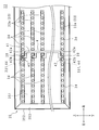
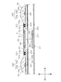
- 7 and 8 are cross-sectional views schematically showing configurations in the vicinity of the light source substrate 33 and the power supply unit 37 of the illumination device 22.
- the display device 13 and the illumination device 22 of the present embodiment have substantially the same configuration as the display device 13 and the illumination device 22 of the first embodiment.
- differences from the first embodiment will be described, and other parts corresponding to those of the first embodiment are denoted by the same reference numerals and description thereof will be omitted.
- the light source substrate 33 of the present embodiment is not provided with the connector 331 and the through hole 332 of the first embodiment.
- a connector 333 is provided on the front surface 33 a of the light source substrate 33.
- the connector 333 has the same configuration as the connector 331 of the first embodiment except for the arrangement position.
- the connector 333 is arranged at the center in the width direction of one short side (that is, the end in the length direction) of the light source substrate 33.
- the connectors 333 and 333 of the two light source boards 33 and 33 adjacent in the left-right direction are arranged on the end portions of the light source boards 33 and 33 that are arranged to face each other. That is, in the case of each light source board 33 included in the left one row, the connector 333 is arranged on the right side. In the case of each light source substrate 33 included in the right column, the connector 333 is arranged on the left side.
- the through holes 354, 354,... Of the first embodiment are not provided.
- a through hole 355 is provided in the bottom wall 351.
- the arrangement position of the through hole 355 is the central portion of the bottom wall 351 in the vertical and horizontal directions.
- the reflection sheet 36 is not provided with the through holes 361, 361,... Of the first embodiment.
- the connector 333 of each light source substrate 33 is covered with the reflection sheet 36. Illustration of the reflection sheet 36 in FIGS. 7 and 8 is omitted.
- the power supply unit 37 has a male connector 371.
- the connector 371 is inserted into the through hole 355 of the bottom wall 351 from the back side and protrudes into the housing body 35.
- the height of the connector 371 from the front surface of the bottom wall 351 is lower than the height of the light source substrate 33 from the front surface of the bottom wall 351.
- the lighting device 22 of the present embodiment does not include the wiring members 38 and 38 but includes the power supply member 5 instead of the power supply members 4 and 4.
- the power supply member 5 is for supplying power from the power supply unit 37 to each light source substrate 33.
- the two power supply members 4 and 4 are arranged on the left and right sides to supply power to the light source boards 33, 33,... In the left and right rows. Power is supplied to the left and right light source boards 33, 33,.
- the power supply member 5 uses a flexible printed circuit board whose base film has translucency, and is arranged between the bottom wall 351 and the reflection sheet 36. Since the power supply member 5 is sufficiently thin, there is no possibility that the bottom wall 351 and the reflection sheet 36 are unnecessarily separated due to the presence of the power supply member 5.
- the power supply member 5 includes polyethylene terephthalate resin or polyethylene naphthalate resin. Therefore, the power supply member 5 is less expensive than a general flexible printed board including a polyimide resin. Moreover, if a polyethylene terephthalate resin or a polyethylene naphthalate resin is used, a flexible printed board having translucency can be obtained easily and inexpensively.
- the power supply member 5 includes a main body 51, a plurality of arm-like pieces 521, 521,... And a plurality of tongue-like pieces 522, 522,.
- the number of arm-shaped pieces 521, 521,... Is the same as the number of light source substrates 33, 33,.
- the number of tongue pieces 522, 522,... Is, for example, four.
- a plurality of light source connection portions 54, 54,... And a power supply connection portion 55 are provided on one surface of the power supply member 5, and a power supply path for individually connecting the power supply connection portion 55 and each light source connection portion 54. Is formed. Since the light source connection parts 54, 54,... And the power supply connection part 55 are provided on the same surface of the power supply member 5, compared with the case where these are provided individually on different surfaces of the power supply member 5. The manufacturing cost is reduced.
- the number of light source connection portions 54, 54,... Is the same as the number of arm-like pieces 521, 521,.
- the main body 51 is formed in a strip shape that is long in the vertical direction.
- the position of the main body 51 is between the light source substrates 33, 33,... On the left side and the light source substrates 33, 33,. That is, the main body 51 does not cover the light source substrate 33.
- the upper end (or lower end) of the main body 51 is disposed between the two light source substrates 33 and 33 adjacent in the left-right direction at the uppermost position (or the lowermost position).
- a power connection 55 is provided at the center in the vertical direction of the main body 51.
- the power supply connection portion 55 includes a female connector 551 corresponding to the connector 371 of the power supply portion 37 and a connection support portion 552 that supports the connector 551.
- the power supply connecting portion 55 is electrically connected to the connector 371 by fitting the connector 551 to the connector 371 from the front side.
- connection support portion 552 is for arranging the connector 551 separately from the main body portion 51 on the rear side, and electrically connecting the connector 551 and the power supply path formed in the main body portion 51.
- connection support part 552 is interposed between the connector 551 and the main body part 51, the main body part 51 is bent unnecessarily to the rear side because the power supply connection part 55 is connected to the connector 371. It is suppressed.
- the power supply member 5 is electrically connected to the power supply unit 37 via the power supply connection unit 55 and the connector 371. As a result, each light source substrate 33 and the power supply unit 37 are individually electrically connected via the power supply member 5.
- Each arm-shaped piece 521 of the power supply member 5 has a rectangular tongue shape whose length direction is the left-right direction.
- Each of the arm-shaped pieces 521, 521,... Protrudes from the main body 51 in the left-right direction. That is, the arm-shaped pieces 521, 521,... Are arranged in 10 rows and 2 columns.
- the arm-shaped piece 521 at the uppermost position (or the lowermost position) protrudes from the uppermost end (or the lowermost end) of the main body 51.
- the direction in which each arm-shaped piece 521 protrudes from the main body 51 and the length of protrusion are the same. Since the power supply member 5 is flexible, each arm-shaped piece 521 can be arranged with the boundary with the main body 51 as a center. Therefore, the arm-shaped pieces 521 are arranged obliquely with respect to the main body 51. be able to.
- the light source connection portion 54 is provided at the distal end portion of the arm-shaped piece 521.
- the light source connection portion 54 is a female connector corresponding to the connector 333.
- the light source connection portion 54 is electrically connected to the connector 333 by being fitted to the connector 333 from the front side. Since the light source connection portion 54 is provided on the arm-shaped piece 521, it is easier to adjust the arrangement position of the light source connection portion 54 than when the light source connection portion 54 is provided on the main body portion 51. Therefore, even if a relative positional shift between the main body 51 and the light source substrates 33, 33,... Due to a dimensional error or a layout trouble, or a positional shift due to expansion / contraction due to a temperature change occurs, the light source The connecting portion 54 and the connector 333 can be easily connected, and unnecessary disconnection is suppressed.
- the work of connecting the light source connection portion 54 to the connector 333 by the manufacturer is highly workable. This is because the power supply member 5 has translucency, so that even if the power supply member 5 covers the connector 333, the arrangement position of the connector 333 can be easily confirmed through the power supply member 5.
- Each arm-shaped piece 521 covers a portion where the connector 333 of the light source board 33 is provided. Since the connector 333 is provided on the short side portion of the light source substrate 33, the power supply member 5 does not unnecessarily cover the light source substrate 33.
- Each tongue-like piece 522 of the power supply member 5 has a rectangular tongue shape whose length direction is the left-right direction.
- the upper (or lower) tongue-like piece 522 is disposed between the uppermost (or lowermost) light source substrate 33 and the lower (or upper) light source substrate 33 adjacent thereto. That is, each tongue-like piece 522 does not cover the light source substrate 33.
- a through hole (not shown) is provided at the tip of the tongue-like piece 522.
- a through hole (not shown) corresponding to the through hole is provided in the reflection sheet 36.
- the tongue-like pieces 522, 522,... And the reflection sheet 36 are fastened to the bottom wall 351 by using fastening members 39, 39,. Therefore, compared with the case where these are individually fixed to the bottom wall 351 by different fixing members, the number of parts and the number of parts can be reduced.
- Each tongue-like piece 522 is fixed to the bottom wall 351 by being fastened together with the reflection sheet 36.
- the power supply member 5 is urged toward the bottom wall 351 and the light source connecting portion 54 is pressed against the connector 333, so that the light source connecting portion 54 is detached from the connector 333 and the electrical connection between them is unnecessarily released. Is also suppressed.
- the tongue-like pieces 522, 522,... May be closely fixed to the bottom wall 351 independently of the reflection sheet 36 or using a fixing member other than the joint members 39, 39,.
- the illumination device 22 In the case of the illumination device 22 as described above, power is supplied from the power supply unit 37 to the light sources 34 via the power supply member 5 and the light source substrates 33, 33,. As a result, the illuminating device 22 can achieve the same effects as the illuminating device 22 of the first embodiment. Moreover, the illumination device 22 of the first embodiment includes two power supply members 4 and 4 and is connected to the power supply unit 37 via the wiring members 38 and 38, whereas the illumination of the present embodiment. Since the device 22 includes one power supply member 5 and is directly connected to the power supply unit 37, the number of components can be reduced.
- each light source substrate 33 in the left-right direction since the arm-shaped piece 521 is pulled out from each light source substrate 33 in the left-right direction, it is not necessary to pull out the arm-shaped piece 521 to the upper side or the lower side of the bottom wall 351.
- the connector 333 of each light source board 33 is provided at the end of the bottom wall 351 of the light source board 33 on the center side in the left-right direction. Therefore, there is no need to pull out the arm-shaped piece 521 to the left side or right side of the bottom wall 351.
- the power supply member 5 is not disposed on the upper side (or lower side) of the bottom wall 351 with respect to the light source substrates 33 and 33 at the uppermost position (or the lowermost position). Further, the power supply member 5 is not arranged on the left side (or right side) of the bottom wall 351 with respect to the left (or right) row of light source boards 33, 33,. As a result, the light source substrates 33, 33,... Can be disposed on the periphery of the bottom wall 351, so that the light sources 34, 34,. Therefore, the luminance of the peripheral edge of the display area of the display panel 21 can be improved. Further, since the space on the bottom wall 351 is not wasted, the number of light source substrates 33, 33,... Arranged on the bottom wall 351 can be increased. As many light sources 34, 34,... Can be arranged accordingly, the luminance of the entire display area of the display panel 21 can be improved.
- FIG. 9 is a cross-sectional view schematically showing a configuration in the vicinity of the power supply unit 37 of the illumination device 22 included in the display device 13 according to Embodiment 3 of the present invention.
- FIG. 9 corresponds to FIGS. 7 and 8 of the second embodiment.
- the display device 13 and the illumination device 22 of the present embodiment have substantially the same configuration as the display device 13 and the illumination device 22 of the second embodiment. In the following, differences from the second embodiment will be described, and other parts corresponding to the second embodiment are denoted by the same reference numerals and description thereof will be omitted.
- the power supply connection portion 55 of the power supply member 5 is directly provided on the main body 51 corresponding to the connector 551 of the second embodiment, and does not have the connection support portion 552 of the second embodiment. For this reason, the power feeding member 5 of the present embodiment has a simpler configuration than that of the second embodiment.
- the connector 371 of the power supply unit 37 is not inserted into the through hole 355 of the bottom wall 351, and is located outside the container 35.
- the lighting device 22 includes a wiring member 38.
- the wiring member 38 is drawn into and out of the housing body 35 through the through hole 355 of the bottom wall 351, and electrically connects the power supply connection portion 55 of the power supply member 5 and the connector 371 of the power supply portion 37.
- the wiring member 38 includes a male connector 381 corresponding to the power supply connection portion 55 and a female connector 382 corresponding to the connector 371.
- each light source substrate 33 and the power supply unit 37 are individually electrically connected via the power supply member 5.
- the lighting device 22 as described above has the same operational effects as the lighting device 22 of the second embodiment. Further, since the wiring member 38 is interposed between the connector 371 and the power supply connection portion 55, the main body portion 51 may be bent unnecessarily to the rear side because the power supply connection portion 55 is connected to the connector 371. It is suppressed.
- the illuminating device 22 includes a dish-shaped container 35, a light source 34 mounted on one surface thereof, and a plurality of light source substrates 33 juxtaposed on the inner surface of the bottom wall 351 of the container 35.
- the lighting device 22 that includes the reflection sheet 36 that covers the one surface and the inner surface of the container 35 and reflects light, and a power supply unit 37, connectors 331 and 333 provided on the one surface and a flexible printed circuit board are used.
- the power supply members 4 and 5 are arranged between the bottom wall 351 and the reflection sheet 36 to supply power from the power supply unit 37 to the light source substrate 33, and are provided on the power supply members 4 and 5.
- light source connection portions 44 and 54 electrically connected to the connectors 331 and 333.
- the power supply members 4 and 5 have a strip shape and are electrically connected to the power supply unit 37, the light source substrate 33 has a strip shape, and the power supply members 4 and 5 The light source substrates 33 are juxtaposed in the width direction along the length direction.
- the power supply member 5 has a belt shape and is electrically connected to the power supply unit 37, and the ends of the two light source substrates 33 are arranged in the width direction of the power supply member 5. Are adjacent to each other, and the connector 333 is arranged at the end.
- the light source 34 includes a light emitting unit 341 mounted on the one surface, a light incident unit 34a that covers the light emitting unit 341, and the light emitted from the light emitting unit 341 enters the light source 34a.
- a through hole 355 is provided in the bottom wall 351, and the power supply unit 37 is disposed on an outer surface of the bottom wall 351, and the power feeding member is passed through the through hole 355. 5 is electrically connected.
- the illuminating device 22 according to the present invention is characterized in that the light source connecting portion 54 and the power source connecting portion 55 for electrical connection with the power source portion 37 are provided on one surface of the power supply member 5. And
- the portion of the power supply member 5 where the light source connection portion 54 is provided covers the connector 333, and the power supply member 5 has a tongue-like piece 522.
- the shape piece 522 is characterized in that it is tightly fixed to the bottom wall 351.
- the power supply members 4 and 5 include strip-shaped main body portions 41 and 51, and a plurality of arm-shaped pieces 42 and 521 protruding from the main body portions 41 and 51, The arm-shaped pieces 42 and 521 are provided with the light source connection portions 44 and 54, respectively.
- the illuminating device 22 according to the present invention is characterized in that each light source substrate 33 and the power supply unit 37 are individually electrically connected via the power feeding members 4 and 5.
- the display device 13 according to the present invention includes the illumination device 22 according to the present invention and a display panel 21 illuminated from the back side by the illumination device 22.
- the television receiver includes a display device 13 according to the present invention and a receiving unit 11 that receives a television broadcast, and displays video on the display device 13 based on the television broadcast received by the receiving unit. It is made to do so.
- the power supply member uses a flexible printed circuit board. Therefore, the wiring is simpler than in the case where a plurality of power supply lines are electrically connected to each light source substrate.
- strip-like light source substrates are juxtaposed in the width direction along the length direction of the belt-shaped power supply member. Therefore, the number of light source substrates fed via the power feeding member can be increased more easily than when strip-shaped light source substrates are juxtaposed along the length direction of the belt-shaped power feeding member. .
- the connector is provided at each of the opposing end portions of the two adjacent light source boards, so that compared to the case where the connector is provided at other than the opposing end portions of the two adjacent light source boards.
- twice as many light source substrates can be easily connected to the power supply member. Therefore, if the number of light source substrates is the same, the number of power supply members can be reduced.
- the reflection sheet is arranged on the light source substrate side from the light output portion of the light source. Therefore, the reflection sheet and the power supply member or the connector covered with the reflection sheet are prevented from inhibiting light output from the light source.
- the power supply unit and the light source substrate can be electrically connected with a simple configuration through the through hole provided in the bottom wall of the container.
- the light source connecting portion and the power source connecting portion are provided on the same surface of the power feeding member. Therefore, the manufacturing cost of the power feeding member can be reduced as compared with the case where they are provided on different surfaces.
- the power feeding member is generally biased toward the bottom wall. Then, since the light source connection portion is pressed against the connector, it is possible to suppress the unnecessary connection between the power supply member and the connector.
- the arrangement of the individual arm-shaped pieces has a higher degree of freedom than the main body. Therefore, for example, even when a positional shift occurs between the main body and the light source substrate, the generated positional shift can be easily absorbed by the arrangement of the arm-shaped pieces. Therefore, compared with the case where the light source connection part is provided on the main body part, the connection between the light source connection part provided on the arm-shaped piece and the connector is easy, and these connections are unnecessarily released. Is suppressed.
- each light source board and the power supply unit are individually electrically connected via the power supply member, it is possible to cope with local dimming while facilitating wiring.
- FIG. 10 is an enlarged front view schematically showing the configuration of the illumination device 22 included in the display device 13 according to Embodiment 4 of the present invention.
- FIG. 11 is a cross-sectional view schematically showing a configuration in the vicinity of the light source substrate 33 of the illumination device 22. 10 and 11 correspond to FIGS. 3 and 4 of the first embodiment.
- the display device 13 and the illumination device 22 of the present embodiment have substantially the same configuration as the display device 13 and the illumination device 22 of the first embodiment.
- differences from the first embodiment will be described, and other parts corresponding to those of the first embodiment are denoted by the same reference numerals and description thereof will be omitted.
- Each arm-like piece 42 included in the power supply member 4 has a base-side tongue-like piece 42a and a tip-side tongue-like piece 42c corresponding to the tip-side tongue-like piece 42b of the first embodiment.
- the length of the distal tongue piece 42c is about half of the distal tongue piece 42b of the first embodiment.
- the tip side tongue-like piece 42c is not provided with a through hole similar to the through hole 43 of the first embodiment.
- a light source connection portion 44 is provided at the distal end portion of the distal-side tongue-like piece 42c. Also in the present embodiment, the light source connection portion 44 is electrically connected to the connector 331.
- the front-side tongue-like piece 42c is between the two light sources 34, 34 on the front surface 33a of the light source substrate 33 and covers a portion where the connector 331 is provided, but covers a portion where the through hole 332 is provided. Absent. Since the connector 331 is provided on the long side portion of the light source substrate 33 (that is, the end in the width direction of the light source substrate 33), the power supply member 4 does not unnecessarily cover the light source substrate 33.
- the light source substrate 33 and the reflection sheet 36 are fastened to the bottom wall 351 by using a fastening member 39.
- the power feeding member 4 is not fastened to the bottom wall 351 together with the light source substrate 33.
- Each base-side tongue-like piece 42 a and the reflection sheet 36 of the power supply member 4 are fastened to the bottom wall 351 using a fastening member 39.
- the power feeding member 4 is generally biased toward the bottom wall 351 side.
- the light source connection portion 44 is pressed against the connector 331, the connection between the power supply member 4 and the light source substrate 33 is prevented from being unnecessarily released.
- the base side tongue-like piece 42 a is fastened together with the bottom wall 351 together with the reflective sheet 36, the lift of the reflective sheet 36 can be suppressed if the fastened position is in the vicinity of the light source connection portion 44.
- the lighting device 22 as described above has the same operational effects as the lighting device 22 of the first embodiment.
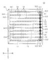
- FIG. 12 is an enlarged front view schematically showing the configuration of the illumination device 22 included in the display device 13 according to Embodiment 5 of the present invention.
- FIG. 12 corresponds to FIG. 10 of the fourth embodiment.
- the display device 13 and the illumination device 22 of the present embodiment have substantially the same configuration as the display device 13 and the illumination device 22 of the fourth embodiment.
- differences from the fourth embodiment will be described, and other parts corresponding to the fourth embodiment will be denoted by the same reference numerals, and description thereof will be omitted.
- the main body 41 of the power supply member 4 is disposed between the light source substrates 33, 33,... And the bottom wall 351. Therefore, the power supply member 4 does not unnecessarily cover the light source substrate 33. Since the power supply member 4 is sufficiently thin, there is no possibility that the bottom wall 351 and each light source substrate 33 are unnecessarily separated due to the presence of the power supply member 4.
- the lighting device 22 as described above has the same operational effects as the lighting device 22 of the fourth embodiment.
- the display device is not limited to the display device 13 configured as the television receiver 1, and may be configured as an electronic signboard, a monitor for a personal computer, or the like. Good.
- the illumination devices according to Embodiments 1 to 6 of the present invention are not limited to the configuration incorporated in the display device 13.
- the lighting device may be configured as a backlight unit of a display unit included in a mobile phone or a portable information terminal device.
- the lighting device may be configured as a ceiling light or a wall-mounted lighting fixture.
- the illuminating device 22 includes a dish-shaped container 35, a light source 34 mounted on one surface thereof, and a plurality of light source substrates 33 juxtaposed on the inner surface of the bottom wall 351 of the container 35.
- the light source substrate 33 has a strip shape, and the length of the light source substrate 33 is
- a connector 331 provided on the one surface of the direction non-end portion and a flexible printed circuit board or a flat cable are used, and are arranged between the bottom wall 351 and the reflection sheet 36, and from the power source unit 37 to the light source
- a power supply member 4 for supplying power to the substrate 33 and a light source connection portion 44 provided on the power supply member 4 and electrically connected to the connector 331 are provided.
- the illuminating device 22 according to the present invention is characterized in that the connector 331 is disposed in two central regions obtained by virtually dividing the light source substrate 33 into four equal parts in the length direction.
- the illuminating device 22 according to the present invention is characterized in that the connector 331 is arranged at an end in the width direction of the light source substrate 33.
- At least one of the light source substrates 33 is disposed on the peripheral portion of the bottom wall 351, and the power supply member 4 is a light source disposed on the peripheral portion of the bottom wall 351. It is characterized by being arranged closer to the center of the bottom wall 351 than the substrate 33.
- the illuminating device 22 according to the present invention is characterized in that the light source substrate 33 or the power feeding member 4 is fastened to the bottom wall 351 together with the reflection sheet 36.
- the display device 13 according to the present invention includes the illumination device 22 according to the present invention and a display panel 21 illuminated from the back side by the illumination device 22.
- the television receiver includes a display device 13 according to the present invention and a receiving unit 11 that receives a television broadcast, and displays video on the display device 13 based on the television broadcast received by the receiving unit. It is made to do so.
- the connector is provided at the non-end portion in the length direction of the light source substrate. That is, the light source board is generally symmetric in the length direction with respect to the connector arrangement position. A light source substrate that is symmetrical in the length direction has substantially the same distance from the power supply unit to the connector even if it is rotated 180 ° in the surface direction of the light source substrate.
- the connector is provided in the central portion in the length direction of the light source substrate. That is, the light source board is highly symmetrical in the length direction with respect to the connector arrangement position.
- the connector is provided at the end in the width direction of the light source substrate. Therefore, compared with the case where the connector is provided at the center in the width direction of the light source substrate, the power supply member connected to the connector does not unnecessarily cover the light source substrate.
- the power feeding member is not arranged on the peripheral edge side of the bottom wall relative to the light source substrate arranged on the peripheral edge of the bottom wall of the container, the container on the bottom wall of the container
- the light source substrate can be disposed close to the boundary with the side wall of the light source.
- the light source substrate or the power supply member and the reflection sheet are fastened together with the bottom wall of the container, the light source substrate or the power supply member and the reflection sheet are individually fixed to the bottom wall of the container. Compared to the case, the number of fixing members can be reduced.
- the light source substrate is substantially symmetrical in the length direction, the light source substrate can be shared. Therefore, the number of parts can be reduced. Therefore, the cost can be reduced by reducing the number of parts.
- the television receiver 1, the display device 13, or the lighting device 22 may include components that are not disclosed in the first to third embodiments.
- the constituent elements (technical features) disclosed in each embodiment can be combined with each other, and a new technical feature can be formed by the combination.
Landscapes
- Physics & Mathematics (AREA)
- Nonlinear Science (AREA)
- Engineering & Computer Science (AREA)
- General Physics & Mathematics (AREA)
- Optics & Photonics (AREA)
- General Engineering & Computer Science (AREA)
- Mathematical Physics (AREA)
- Crystallography & Structural Chemistry (AREA)
- Chemical & Material Sciences (AREA)
- Microelectronics & Electronic Packaging (AREA)
- Planar Illumination Modules (AREA)
- Liquid Crystal (AREA)
- Arrangement Of Elements, Cooling, Sealing, Or The Like Of Lighting Devices (AREA)
Abstract
Priority Applications (4)
| Application Number | Priority Date | Filing Date | Title |
|---|---|---|---|
| JP2017506537A JP6446121B2 (ja) | 2015-03-18 | 2016-03-11 | 照明装置及び表示装置 |
| EP16764917.7A EP3273156B1 (fr) | 2015-03-18 | 2016-03-11 | Dispositif d'éclairage et dispositif d'affichage |
| US15/554,469 US10180532B2 (en) | 2015-03-18 | 2016-03-11 | Illumination device and display device |
| CN201680012931.0A CN107407477A (zh) | 2015-03-18 | 2016-03-11 | 照明装置和显示装置 |
Applications Claiming Priority (4)
| Application Number | Priority Date | Filing Date | Title |
|---|---|---|---|
| JP2015054857 | 2015-03-18 | ||
| JP2015-054857 | 2015-03-18 | ||
| JP2015-054856 | 2015-03-18 | ||
| JP2015054856 | 2015-03-18 |
Publications (1)
| Publication Number | Publication Date |
|---|---|
| WO2016148087A1 true WO2016148087A1 (fr) | 2016-09-22 |
Family
ID=56920394
Family Applications (1)
| Application Number | Title | Priority Date | Filing Date |
|---|---|---|---|
| PCT/JP2016/057858 Ceased WO2016148087A1 (fr) | 2015-03-18 | 2016-03-11 | Dispositif d'éclairage et dispositif d'affichage |
Country Status (5)
| Country | Link |
|---|---|
| US (1) | US10180532B2 (fr) |
| EP (1) | EP3273156B1 (fr) |
| JP (1) | JP6446121B2 (fr) |
| CN (1) | CN107407477A (fr) |
| WO (1) | WO2016148087A1 (fr) |
Cited By (5)
| Publication number | Priority date | Publication date | Assignee | Title |
|---|---|---|---|---|
| WO2018147269A1 (fr) * | 2017-02-09 | 2018-08-16 | パナソニックIpマネジメント株式会社 | Dispositif d'affichage d'images |
| JP2018156923A (ja) * | 2017-03-20 | 2018-10-04 | 高▲徳▼ ▲蔡▼ | Led面光源ランプ |
| US20190129230A1 (en) * | 2017-02-09 | 2019-05-02 | Panasonic Intellectual Property Management Co., Ltd. | Image display apparatus |
| WO2020039721A1 (fr) * | 2018-08-22 | 2020-02-27 | ソニー株式会社 | Dispositif d'éclairage et dispositif d'affichage |
| JP2023144010A (ja) * | 2019-06-27 | 2023-10-06 | コイズミ照明株式会社 | 照明器具 |
Families Citing this family (5)
| Publication number | Priority date | Publication date | Assignee | Title |
|---|---|---|---|---|
| CN110285393B (zh) * | 2019-05-31 | 2020-08-28 | 中山市超质光电有限公司 | 一种新型led灯及其装配方法 |
| CN117157567A (zh) * | 2021-08-17 | 2023-12-01 | 三星电子株式会社 | 显示装置和背光单元 |
| CN113775985A (zh) * | 2021-10-15 | 2021-12-10 | 苏州欧普照明有限公司 | 照明装置及吸顶灯 |
| EP4517415A4 (fr) * | 2022-09-22 | 2025-08-06 | Lg Electronics Inc | Dispositif d'affichage |
| AU2024200126B2 (en) * | 2023-01-11 | 2025-09-04 | Lg Electronics Inc. | Display device |
Citations (3)
| Publication number | Priority date | Publication date | Assignee | Title |
|---|---|---|---|---|
| JP2010062456A (ja) * | 2008-09-05 | 2010-03-18 | Sharp Corp | 光源、映像表示装置、および照明装置、ならびにそれらの製造方法 |
| JP2013229232A (ja) * | 2012-04-26 | 2013-11-07 | Sharp Corp | 照明装置、表示装置、及びテレビ受信装置 |
| JP2014206641A (ja) * | 2013-04-12 | 2014-10-30 | 船井電機株式会社 | 表示装置およびバックライト |
Family Cites Families (11)
| Publication number | Priority date | Publication date | Assignee | Title |
|---|---|---|---|---|
| JP2724642B2 (ja) * | 1991-09-10 | 1998-03-09 | シャープ株式会社 | 液晶表示装置 |
| JPWO2006059464A1 (ja) * | 2004-11-30 | 2008-06-05 | シャープ株式会社 | ランプ保持具及びそれを用いた表示装置用照明装置及びそれを用いた表示装置及び表示装置用照明装置を用いた液晶表示装置 |
| CN102809091B (zh) * | 2007-03-08 | 2015-04-08 | 夏普株式会社 | Led背光源和液晶显示装置 |
| JP4599470B2 (ja) | 2009-04-28 | 2010-12-15 | シャープ株式会社 | 基板保持具、電子装置及び表示装置 |
| CN102439354B (zh) * | 2009-05-22 | 2015-04-08 | 夏普株式会社 | 光源装置、照明装置、背光源装置、液晶显示装置及显示装置 |
| JP4519943B1 (ja) * | 2009-05-22 | 2010-08-04 | シャープ株式会社 | 表示装置 |
| JP5351723B2 (ja) * | 2009-05-22 | 2013-11-27 | シャープ株式会社 | 光源装置及び表示装置 |
| US8636382B2 (en) * | 2009-06-25 | 2014-01-28 | Sharp Kabushiki Kaisha | Light source apparatus, image display apparatus and television receiving apparatus |
| JP5258978B2 (ja) * | 2010-01-12 | 2013-08-07 | シャープ株式会社 | Led基板、バックライトユニットおよび液晶表示装置 |
| JP2012013722A (ja) | 2010-06-29 | 2012-01-19 | Funai Electric Co Ltd | 液晶モジュール |
| JP5735439B2 (ja) | 2012-02-10 | 2015-06-17 | シャープ株式会社 | 実装基板の固定部材、照明装置および液晶表示装置 |
-
2016
- 2016-03-11 WO PCT/JP2016/057858 patent/WO2016148087A1/fr not_active Ceased
- 2016-03-11 US US15/554,469 patent/US10180532B2/en active Active
- 2016-03-11 CN CN201680012931.0A patent/CN107407477A/zh active Pending
- 2016-03-11 EP EP16764917.7A patent/EP3273156B1/fr active Active
- 2016-03-11 JP JP2017506537A patent/JP6446121B2/ja active Active
Patent Citations (3)
| Publication number | Priority date | Publication date | Assignee | Title |
|---|---|---|---|---|
| JP2010062456A (ja) * | 2008-09-05 | 2010-03-18 | Sharp Corp | 光源、映像表示装置、および照明装置、ならびにそれらの製造方法 |
| JP2013229232A (ja) * | 2012-04-26 | 2013-11-07 | Sharp Corp | 照明装置、表示装置、及びテレビ受信装置 |
| JP2014206641A (ja) * | 2013-04-12 | 2014-10-30 | 船井電機株式会社 | 表示装置およびバックライト |
Cited By (18)
| Publication number | Priority date | Publication date | Assignee | Title |
|---|---|---|---|---|
| US10705364B2 (en) | 2017-02-09 | 2020-07-07 | Panasonic Intellectual Property Management Co., Ltd. | Image display apparatus |
| US20190129230A1 (en) * | 2017-02-09 | 2019-05-02 | Panasonic Intellectual Property Management Co., Ltd. | Image display apparatus |
| JPWO2018147269A1 (ja) * | 2017-02-09 | 2019-12-12 | パナソニックIpマネジメント株式会社 | 画像表示装置 |
| WO2018147269A1 (fr) * | 2017-02-09 | 2018-08-16 | パナソニックIpマネジメント株式会社 | Dispositif d'affichage d'images |
| EP3582209A4 (fr) * | 2017-02-09 | 2020-05-13 | Panasonic Intellectual Property Management Co., Ltd. | Dispositif d'affichage d'images |
| JP2018156923A (ja) * | 2017-03-20 | 2018-10-04 | 高▲徳▼ ▲蔡▼ | Led面光源ランプ |
| US10184638B2 (en) | 2017-03-20 | 2019-01-22 | Kao-Teh CHAI | LED plane light source lamp |
| JPWO2020039721A1 (ja) * | 2018-08-22 | 2021-08-26 | ソニーグループ株式会社 | 照明装置及び表示装置 |
| WO2020039721A1 (fr) * | 2018-08-22 | 2020-02-27 | ソニー株式会社 | Dispositif d'éclairage et dispositif d'affichage |
| US11359805B2 (en) | 2018-08-22 | 2022-06-14 | Saturn Licensing Llc | Lighting device and display device |
| US11668459B2 (en) | 2018-08-22 | 2023-06-06 | Saturn Licensing Llc | Lighting device and display device |
| JP7357187B2 (ja) | 2018-08-22 | 2023-10-06 | サターン ライセンシング エルエルシー | 照明装置及び表示装置 |
| JP2023156405A (ja) * | 2018-08-22 | 2023-10-24 | サターン ライセンシング エルエルシー | 表示装置 |
| US12072090B2 (en) | 2018-08-22 | 2024-08-27 | Saturn Licensing Llc | Lighting device and display device |
| JP7574369B2 (ja) | 2018-08-22 | 2024-10-28 | サターン ライセンシング エルエルシー | 表示装置 |
| JP2024180601A (ja) * | 2018-08-22 | 2024-12-26 | サターン ライセンシング エルエルシー | 表示装置 |
| JP7850782B2 (ja) | 2018-08-22 | 2026-04-23 | サターン ライセンシング エルエルシー | 表示装置 |
| JP2023144010A (ja) * | 2019-06-27 | 2023-10-06 | コイズミ照明株式会社 | 照明器具 |
Also Published As
| Publication number | Publication date |
|---|---|
| JPWO2016148087A1 (ja) | 2017-12-07 |
| CN107407477A (zh) | 2017-11-28 |
| EP3273156B1 (fr) | 2020-11-18 |
| US10180532B2 (en) | 2019-01-15 |
| JP6446121B2 (ja) | 2018-12-26 |
| EP3273156A1 (fr) | 2018-01-24 |
| EP3273156A4 (fr) | 2018-03-28 |
| US20180045877A1 (en) | 2018-02-15 |
Similar Documents
| Publication | Publication Date | Title |
|---|---|---|
| JP6446121B2 (ja) | 照明装置及び表示装置 | |
| CN100397196C (zh) | 背光设备和液晶显示器 | |
| US8721159B2 (en) | Lighting device, display device and television receiver | |
| US20110075443A1 (en) | Light emitting unit, backlight module and display device | |
| CN108022520A (zh) | 显示装置 | |
| CN102314021A (zh) | 液晶显示器 | |
| JP2011003549A (ja) | 光源装置及びこれを備える表示装置、テレビ受像装置 | |
| JP2012013722A (ja) | 液晶モジュール | |
| US20150070592A1 (en) | Liquid crystal display apparatus and television receiver | |
| US8591091B2 (en) | Surface light source device and display device | |
| US10914985B2 (en) | Image display apparatus and support pin | |
| JP6827183B2 (ja) | 表示装置 | |
| EP3163365B1 (fr) | Appareil d'affichage | |
| US9581846B2 (en) | Display device and television device | |
| WO2014141882A1 (fr) | Appareil d'affichage et appareil récepteur de télévision | |
| US10914984B2 (en) | Image display apparatus and support pin | |
| JP2018084639A (ja) | 光出射ユニット、取付ベース及び表示装置 | |
| WO2013191047A1 (fr) | Dispositif d'affichage et récepteur de télévision | |
| JP6975904B2 (ja) | 画像表示装置 | |
| WO2013065539A1 (fr) | Dispositif d'éclairage, dispositif d'affichage et dispositif de réception de télévision | |
| JP2017045532A (ja) | 照明装置、表示装置、及びテレビジョン受信機 | |
| KR101401256B1 (ko) | 발광다이오드 모듈과 이를 포함하는 백라이트 유닛 및 디스플레이 장치 | |
| EP2857924A2 (fr) | Appareil d'affichage vidéo | |
| JP7396925B2 (ja) | 電子機器 | |
| JP2023083651A (ja) | 表示装置および表示システム |
Legal Events
| Date | Code | Title | Description |
|---|---|---|---|
| 121 | Ep: the epo has been informed by wipo that ep was designated in this application |
Ref document number: 16764917 Country of ref document: EP Kind code of ref document: A1 |
|
| ENP | Entry into the national phase |
Ref document number: 2017506537 Country of ref document: JP Kind code of ref document: A |
|
| REEP | Request for entry into the european phase |
Ref document number: 2016764917 Country of ref document: EP |
|
| WWE | Wipo information: entry into national phase |
Ref document number: 15554469 Country of ref document: US |
|
| NENP | Non-entry into the national phase |
Ref country code: DE |