WO2016158048A1 - Résonateur - Google Patents
Résonateur Download PDFInfo
- Publication number
- WO2016158048A1 WO2016158048A1 PCT/JP2016/054440 JP2016054440W WO2016158048A1 WO 2016158048 A1 WO2016158048 A1 WO 2016158048A1 JP 2016054440 W JP2016054440 W JP 2016054440W WO 2016158048 A1 WO2016158048 A1 WO 2016158048A1
- Authority
- WO
- WIPO (PCT)
- Prior art keywords
- electrode
- arm
- holding
- holding arm
- vibration
- Prior art date
- Legal status (The legal status is an assumption and is not a legal conclusion. Google has not performed a legal analysis and makes no representation as to the accuracy of the status listed.)
- Ceased
Links
Images


Classifications
-
- H—ELECTRICITY
- H03—ELECTRONIC CIRCUITRY
- H03H—IMPEDANCE NETWORKS, e.g. RESONANT CIRCUITS; RESONATORS
- H03H9/00—Networks comprising electromechanical or electro-acoustic elements; Electromechanical resonators
- H03H9/24—Constructional features of resonators of material which is not piezoelectric, electrostrictive, or magnetostrictive
- H03H9/2405—Constructional features of resonators of material which is not piezoelectric, electrostrictive, or magnetostrictive of microelectro-mechanical resonators
-
- H—ELECTRICITY
- H03—ELECTRONIC CIRCUITRY
- H03H—IMPEDANCE NETWORKS, e.g. RESONANT CIRCUITS; RESONATORS
- H03H9/00—Networks comprising electromechanical or electro-acoustic elements; Electromechanical resonators
- H03H9/02—Details
- H03H9/02244—Details of microelectro-mechanical resonators
- H03H9/02338—Suspension means
-
- H—ELECTRICITY
- H03—ELECTRONIC CIRCUITRY
- H03H—IMPEDANCE NETWORKS, e.g. RESONANT CIRCUITS; RESONATORS
- H03H9/00—Networks comprising electromechanical or electro-acoustic elements; Electromechanical resonators
- H03H9/02—Details
- H03H9/02244—Details of microelectro-mechanical resonators
- H03H9/02433—Means for compensation or elimination of undesired effects
-
- H—ELECTRICITY
- H03—ELECTRONIC CIRCUITRY
- H03H—IMPEDANCE NETWORKS, e.g. RESONANT CIRCUITS; RESONATORS
- H03H9/00—Networks comprising electromechanical or electro-acoustic elements; Electromechanical resonators
- H03H9/02—Details
- H03H9/05—Holders or supports
- H03H9/0595—Holders or supports the holder support and resonator being formed in one body
-
- H—ELECTRICITY
- H03—ELECTRONIC CIRCUITRY
- H03H—IMPEDANCE NETWORKS, e.g. RESONANT CIRCUITS; RESONATORS
- H03H9/00—Networks comprising electromechanical or electro-acoustic elements; Electromechanical resonators
- H03H9/02—Details
- H03H9/05—Holders or supports
- H03H9/10—Mounting in enclosures
- H03H9/1057—Mounting in enclosures for microelectro-mechanical devices
-
- H—ELECTRICITY
- H03—ELECTRONIC CIRCUITRY
- H03H—IMPEDANCE NETWORKS, e.g. RESONANT CIRCUITS; RESONATORS
- H03H9/00—Networks comprising electromechanical or electro-acoustic elements; Electromechanical resonators
- H03H9/02—Details
- H03H9/02244—Details of microelectro-mechanical resonators
- H03H9/02338—Suspension means
- H03H2009/02385—Anchors for square resonators, i.e. resonators comprising a square vibrating membrane
-
- H—ELECTRICITY
- H03—ELECTRONIC CIRCUITRY
- H03H—IMPEDANCE NETWORKS, e.g. RESONANT CIRCUITS; RESONATORS
- H03H9/00—Networks comprising electromechanical or electro-acoustic elements; Electromechanical resonators
- H03H9/02—Details
- H03H9/02244—Details of microelectro-mechanical resonators
- H03H9/02433—Means for compensation or elimination of undesired effects
- H03H2009/0244—Anchor loss
Definitions
- the present invention relates to a resonator.
- a piezoelectric vibrator is used as a device for realizing a timekeeping function in an electronic device. Along with the downsizing of electronic equipment, the piezoelectric vibrator is also required to be downsized, and a resonator manufactured using a MEMS (Micro Electro Mechanical Systems) technique has been attracting attention.
- MEMS Micro Electro Mechanical Systems
- a conventional resonator includes a rectangular vibrating portion, electrodes formed on the vibrating portion, a holding arm that connects the vibrating portion and the holding portion, and a holding arm. It is comprised from the wiring which leads the electrode provided on the holding
- the holding arm has an elongated shape so as not to disturb the vibration of the vibrating part.
- the resonance resistance in the holding arm is increased, and on the contrary, the vibration of the vibrating portion is hindered. There is.
- the present invention has been made in view of such circumstances, and an object thereof is to reduce the resonance resistance in the holding arm.
- a resonator includes a vibration unit including a first electrode and a second electrode, and a piezoelectric film formed between the first electrode and the second electrode, and vibration.
- the first electrode or the second electrode is formed over the holding arm and is connected to the extraction electrode on the holding arm, and the electric resistance value per unit area of the extraction electrode is determined by the holding arm.
- the electric resistance value per unit area of the first electrode or the second electrode formed over the entire area is smaller.
- the upper electrode on the holding arm is configured to be extracted by the extraction electrode having a smaller electric resistance value per unit area than the upper electrode. Therefore, the resonance resistance in the holding arm can be reduced.
- the holding arm further has an insulating protective film on the first electrode or the second electrode formed over the holding arm, and the lead electrode is connected via a via penetrating the protective film, It is preferable to connect to the first electrode or the second electrode formed over the holding arm.
- the lead electrode and the electrode can be connected on the holding arm.
- both the first electrode and the second electrode are formed over the holding arm, and the extraction electrode is connected to the first electrode or the second electrode.
- both the upper electrode and the lower electrode can be connected by the extraction electrode.
- the holding arm includes a first arm provided in a direction substantially parallel to one side of the vibration unit, and a second arm provided in a direction substantially perpendicular to the first arm and connecting the first arm and the vibration unit.
- the lead electrode is preferably connected to the first electrode or the second electrode through a via at a connection point between the first arm and the second arm.
- the rigidity and mass of the bent portion can be increased by providing a via in the bent portion of the holding arm.
- the acoustic reflection effect at the bent portion can be enhanced and the vibration confinement can be improved.
- the holding arms are provided in a direction substantially perpendicular to the pair of first arms and the pair of first arms provided in a direction substantially parallel to one side of the vibration unit, and the pair of first arms is provided at both ends thereof.
- a vibration buffer formed by a pair of second arms connected to both ends of one arm, and the extraction electrode is connected to the vibration buffer at a connection point between the first arm and the pair of second arms.
- the first electrode or the second electrode is preferably connected via a via.
- the resonance resistance in the holding arm is reduced.
- FIG. 1 is an exploded perspective view schematically showing a structure of a resonance device according to a first embodiment. It is a top view which shows roughly an example of the structure of the resonator which concerns on 1st Embodiment. It is a figure which shows roughly an example of the structure of the cross section of the resonator which concerns on 1st Embodiment. It is a figure which shows roughly an example of the structure of the cross section of the resonator which concerns on 1st Embodiment. It is a top view which shows roughly an example of the structure of the resonator which concerns on 2nd Embodiment. It is a top view which shows roughly an example of the structure of the resonator which concerns on 3rd Embodiment.
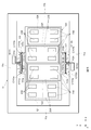
- FIG. 1 is a perspective view schematically showing the appearance of the resonance device 1 according to the first embodiment of the present invention.
- the resonance device 1 includes a lower substrate 14, an upper substrate 13 that forms a vibration space between the lower substrate 14, and a resonator 10 that is sandwiched and held between the lower substrate 14 and the upper substrate 13.
- the resonator 10 is a MEMS vibrator manufactured using the MEMS technology.
- FIG. 2 is an exploded perspective view schematically showing the structure of the resonance device 1 according to the first embodiment of the present invention.
- the lower substrate 14 extends in a flat plate shape along the XY plane, and a flat rectangular parallelepiped concave portion 17 is formed on the upper surface thereof.
- the recess 17 forms a part of the vibration space of the resonator 10.
- the upper substrate 13 extends in a flat plate shape along the XY plane, and a flat rectangular parallelepiped concave portion 18 is formed on the lower surface thereof.
- the recess 18 forms part of the vibration space of the resonator 10. A vacuum state is maintained in this vibration space.
- the lower substrate 14 and the upper substrate 13 are made of, for example, silicon (Si).
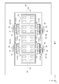
- FIG. 3 is a plan view schematically showing the structure of the resonator 10 according to the present embodiment.
- the resonator 10 includes a vibrating unit 120, a holding frame 11, holding arms 111 and 112, and lead electrodes W111 and W112.
- the vibrating unit 120 has a substantially rectangular parallelepiped outline extending in a flat plate shape along the XY plane in the orthogonal coordinate system of FIG.
- a rectangular plate-shaped upper electrode 121 having a length direction and a width direction is provided on the vibration unit 120.
- the vibration part 120 and the upper electrode 121 have a long side in the X-axis direction and a short side in the Y-axis direction.
- a protective film 235 is formed so as to cover the entire surface of the upper electrode 121. Further, two adjustment films 236 are stacked on the surface of the protective film 235 in parallel with the long side of the vibration unit 120.
- the protective film 235 and the adjustment film 236 are films for adjusting the resonance frequency of the vibration unit 120.
- the adjustment film 236 is formed so that the surface thereof is exposed in a relatively large displacement region in the vibration unit 120. Specifically, the adjustment film 236 is formed so as to be exposed in a region corresponding to the vicinity of both ends in the short side direction of the vibration unit 120. Further, the surface of the protective film 235 is exposed in other regions.
- a space is formed between the vibrating unit 120 and the holding frame 11 at a predetermined interval.
- the vibration unit 120 is connected to and held by the holding frame 11 by holding arms 111 and 112 described later on a pair of short sides.
- the vibrating part 120 is not held by the holding frame 11 in a pair of long sides.
- (1-2. Laminated structure) 4 is a cross-sectional view taken along the line AA ′ of FIG. A laminated structure of the vibration unit 120 will be described with reference to FIG.
- the vibration unit 120 has a lower electrode 129 (an example of a first electrode) stacked on a Si substrate 130 made of degenerate Si.
- the Si substrate 130 has a length of about 140 ⁇ m, a width of about 400 ⁇ m, and a thickness of about 10 ⁇ m.
- the lower electrode 129 is formed using, for example, a metal such as molybdenum (Mo) or aluminum (Al), and has a thickness of about 0.1 ⁇ m. Note that the Si substrate 130 made of degenerated Si may be used as the lower electrode without forming the lower electrode 129.
- a piezoelectric thin film 128 is laminated on the lower electrode 129 so as to cover the lower electrode 129, and an upper electrode 121 (an example of a second electrode) is further formed on the piezoelectric thin film 128.
- the upper electrode 121 may be divided into a plurality of parts.
- the piezoelectric thin film 128 is a piezoelectric thin film that converts an applied voltage into vibration.
- the piezoelectric thin film 128 can be mainly composed of a nitride such as aluminum nitride or an oxide.
- the piezoelectric thin film 128 can be formed of scandium aluminum nitride (ScAlN).
- ScALN is obtained by replacing a part of aluminum (Al) in aluminum nitride (AlN) with scandium (Sc).
- the piezoelectric thin film 128 has a thickness of 0.8 ⁇ m, for example.
- the upper electrode 121 is formed using a metal such as molybdenum (Mo) or aluminum (Al), and has a thickness of about 0.1 ⁇ m.
- a protective film 235 is laminated on the upper electrode 121 so as to cover the upper electrode 121, and an adjustment film 236 is further laminated on the protective film 235. After the adjustment film 236 is formed on substantially the entire surface of the vibration unit 120, the adjustment film 236 is formed only in a predetermined region by processing such as etching.
- the protective film 235 is formed of a material whose mass reduction rate by etching is slower than that of the adjustment film 236.
- the protective film 235 is formed of a nitride film such as AlN or an oxide film such as SiO 2 .
- the mass reduction rate is represented by the product of the etching rate (thickness removed per unit time) and the density.
- the adjustment film 236 is formed of a material whose mass reduction rate by etching is faster than that of the protective film 235.
- the adjustment film 236 is formed of a metal such as molybdenum (Mo), tungsten (W), gold (Au), platinum (Pt), nickel (Ni).
- Mo molybdenum
- W tungsten
- Au gold
- Pt platinum
- Ni nickel
- the protective film 235 and the adjustment film 236 may have any etching rate relationship as long as the mass reduction rate relationship is as described above.
- Etching of the protective film 235 and the adjustment film 236 is performed, for example, by simultaneously irradiating the protective film 235 and the adjustment film 236 with an ion beam (for example, an argon (Ar) ion beam).
- the ion beam can be irradiated over a wider range than the resonator 10.
- an example is shown in which etching is performed using an ion beam, but the etching method is not limited to that using an ion beam.
- the vibration unit 120 is subjected to contour vibration in the XY plane when an alternating electric field is applied.
- the piezoelectric thin film 128 is oriented in the c-axis direction, so that a predetermined electric field is applied to the upper electrode 121 and the lower electrode 129, and a predetermined potential difference is generated between the lower electrode 129 and the upper electrode 121. Is formed, the piezoelectric thin film 128 expands and contracts in the XY in-plane direction in accordance with the potential difference, so that the vibration unit 120 undergoes contour vibration.
- the main factors that determine the resonance frequency of the vibration unit 120 include mass and spring constant.
- the etching of the protective film 235 and the adjustment film 236 causes a reduction in mass and a reduction in spring constant at the same time. Reducing the mass increases the resonance frequency, and decreasing the spring constant decreases the resonance frequency.
- the influence of the mass is relatively strong in the region where the displacement is large, and the influence of the spring constant is relatively strong in the region where the displacement is small.
- an adjustment film 236 is formed so as to be exposed in a region where the displacement is relatively large.
- the adjustment film 236 has a higher mass reduction rate by the ion beam than the protective film 235. For this reason, the mass of the region having a relatively large displacement is quickly reduced. Thereby, the resonance frequency can be raised.
- the protective film 235 is etched simultaneously with the adjustment film 236, the amount of change in the spring constant is small because the mass reduction rate is slower than that of the adjustment film 236. Therefore, the influence of the decrease in the resonance frequency accompanying the change in the spring constant is small. Therefore, in the vibration unit 120, it is possible to efficiently adjust the resonance frequency by simultaneously irradiating the protective film 235 and the adjustment film 236 with the ion beam.
- the temperature characteristics of the resonance frequency are affected by changes in the spring constant.
- the vibration unit 120 since the amount of change in the spring constant is small, it is possible to reduce the change in the temperature characteristic of the resonance frequency.
- the holding frame 11 is formed in a rectangular frame shape along the XY plane.
- the holding frame 11 is provided so as to surround the vibration unit 120 and the outside of the vibration unit 120 along the XY plane. More specifically, the holding frame 11 includes a pair of long-side plate-like frames 11 a and 11 b extending in parallel with the X-axis direction so as to face the short side of the vibration unit 120, and the long side of the vibration unit 120. And a pair of short-side frames 11c and 11d that extend in parallel to the Y-axis direction and are connected to both ends of the frames 11a and 11b at both ends thereof, respectively.
- the frame 11c side is described as the upper side of the resonator 10
- the frame 11d side is described as the lower side of the resonator 10.
- a lower wiring W ⁇ b> 129 formed integrally with the lower electrode 129 of the vibration unit 120 is formed on the Si substrate 130. Further, a piezoelectric thin film 128 is laminated so as to cover the lower wiring W 129, and a protective film 235 is laminated on the piezoelectric thin film 128.
- the holding frame 11 is integrally formed with the Si substrate 130, the lower electrode 129, the piezoelectric thin film 128, and the upper electrode 121 of the vibration unit 120 in this order on the Si substrate 130 in the order of the lower wiring W 129, the piezoelectric thin film 128, and the upper wiring W 121 described later. The Thereafter, the upper wiring W121 is removed so as to have a desired shape by processing such as etching, and a protective film 235 is laminated and formed.
- the holding arm 111 is provided inside the holding frame 11 along the XY plane and in a space between the short side of the vibration unit 120 and the frame body 11a, and connects the short side of the vibration unit 120 and the frame body 11a.
- the holding arm 112 is provided in a space between the short side of the vibration unit 120 and the frame 11b, and connects the short side of the vibration unit 120 and the frame 11b.
- FIG. 5A is a BB ′ sectional view of FIG. 3
- FIG. 5B is a CC ′ sectional view of FIG. 3.
- a stacked structure of the holding arms 111 and 112 will be described with reference to FIGS.
- the holding arms 111 and 112 are formed on the Si substrate 130 made of a degenerate semiconductor by the same process as the lower electrode 129 of the vibration unit 120 and the lower wiring W129. Are stacked.
- the lower electrode 129 and the lower wiring W 129 are formed continuously from the vibrating part 120 to the holding arms 111 and 112.
- a piezoelectric thin film 128 is laminated on the lower wiring W129 so as to cover the lower wiring W129.
- an upper wiring W121 integrally formed by the same process as the upper electrode 121 of the vibration unit 120 is provided on the piezoelectric thin film 128, an upper wiring W121 integrally formed by the same process as the upper electrode 121 of the vibration unit 120 is provided.
- the upper electrode 121 and the upper wiring W121 are continuously formed from the vibrating portion 120 to the holding arms 111 and 112.
- the Si substrate 130, the lower wiring W 129, the piezoelectric thin film 128, and the upper wiring W 121 of the holding arms 111 and 112 are integrally formed with the Si substrate 130, the lower electrode 129, the piezoelectric thin film 128, and the upper electrode 121 of the vibration unit 120, and etched.
- An upper wiring W121 is removed to form a desired shape by processing, and a protective film 235 is laminated and formed.
- the lead electrode W111 is formed from the frame 11a to the holding arm 111.
- the lead electrode W111 is connected to the upper wiring W121 on the holding arm 111.
- the upper wiring W121 is a wiring in which the upper electrode 121 of the vibration unit 120 is continuously formed to the holding arm 111.
- the upper wiring W121 continuously extends from a connection point between the upper electrode 121 of the vibration unit 120 and the holding arm 111 to a middle point of the holding arm 111 or a connection point between the holding arm 111 and the frame 11a. It is formed to cover.
- the lead electrode W111 is continuously formed from the connection portion with the upper wiring W121 to the frame body 11a.
- the lead electrode W111 is formed so that the electric resistance value per unit area is smaller than that of the upper wiring W121.
- the extraction electrode W111 is formed thicker than the upper wiring W121.
- the lead electrode W111 is a highly conductive metal such as aluminum. Furthermore, the extraction electrode W111 is desirably a light metal. Thereby, it can reduce that the vibration of the vibration part 120 is inhibited by the extraction electrode W111.
- the lead electrode W111 may be formed of the same material as the adjustment film 236 at the same time.
- the lead electrode W111 is formed from the surface of the protective film 235 of the holding arm 111 to the surface of the protective film 235 of the frame 11a.
- the lead electrode W111 is connected to the upper wiring W121 via a via V111 formed through the protective film 235 on the holding arm 111.
- the via V111 is formed, for example, by forming a protective film 235 on the resonator 10 and then removing a part thereof by etching or the like. After the via V111 is formed, a conductive and light metal such as aluminum is laminated on the protective film 235 and the via V111, and a part thereof is removed by etching or the like, thereby forming the extraction electrode W111. Note that the lead electrode W111 may be stacked after the via V111 is filled with metal first.
- the resonator 10 reduces the path resistance in the holding arm 111 by pulling out the upper wiring W121 using the extraction electrode W111 having a smaller electrical resistance value per unit area in the XY plane than the upper electrode 121. Vibration characteristics can be improved.
- the lead electrode W112 is formed from the frame 11b to the holding arm 112.
- the lead electrode W112 is connected to the lower wiring W129 on the holding arm 112.
- the lower wiring W 129 is a wiring in which the lower electrode 129 of the vibration unit 120 is continuously formed to the holding arm 112.
- the lower wiring W129 continuously extends from a connection portion between the lower electrode 129 and the holding arm 112 of the vibration unit 120 to a middle portion of the holding arm 112 or a connection portion between the holding arm 112 and the frame 11b. It is formed to cover.
- the lead electrode W112 is continuously formed from the connection portion with the lower wiring W129 to the frame body 11b.
- the lead electrode W112 is formed so that the electric resistance value per unit area is smaller than that of the lower wiring W129.
- the extraction electrode W112 is formed so as to be thicker than the lower wiring W129.
- the lead electrode W112 is a metal having high conductivity such as aluminum.
- the extraction electrode W112 is preferably a light metal. Thereby, it can reduce that the vibration of the vibration part 120 is inhibited by the extraction electrode W112.
- the extraction electrode W112 may be formed of the same material as the adjustment film 236 at the same time.
- FIG. 5B is a CC ′ sectional view of FIG. With reference to FIG. 5B, a cross-sectional structure of the extraction electrode W112 will be described.
- the lead electrode W112 is formed from the surface of the protective film 235 of the holding arm 112 to the surface of the protective film 235 of the frame 11b.
- the extraction electrode W112 is connected to the lower wiring W129 via a via V112 formed on the holding arm 112 so as to penetrate the protective film 235, the upper wiring W121, and the piezoelectric thin film 128.
- the via V112 and the upper wiring W121 are separated by the piezoelectric thin film 128.
- the via V112 is stacked in the hole after the protective film 235 is filled in the hole formed by removing a part of the upper wiring W121 by etching or the like.
- the protective film 235 and the piezoelectric thin film 128 are partially removed by etching or the like.
- a conductive and light metal such as aluminum is laminated on the protective film 235 and the via V112, and a part thereof is removed by etching or the like, whereby the extraction electrode W112 is formed.
- the lead electrode W112 may be stacked after the via V112 is filled with metal first.
- the resonator 10 reduces the path resistance in the holding arm 112 by pulling out the lower electrode 129 by using the lead electrode W112 having a smaller electrical resistance value per unit area than the lower electrode 129, thereby vibrating the resonator. Characteristics can be improved.
- FIG. 6 is a plan view schematically showing an example of the structure of the resonator 10 according to the present embodiment.
- the detailed configuration of the resonator 10 according to the present embodiment will be described focusing on the differences from the first embodiment.
- the vibration unit 120 includes four upper electrodes 121 to 124.
- the upper electrodes 121 and 123 are connected by a bus bar B121.
- the bus bar B121 is provided at the end portion of the vibration unit 120 so as to face the upper electrode 122.
- the upper electrodes 122 and 124 are connected by a bus bar B122.
- the bus bar B ⁇ b> 122 is provided at the end of the vibration unit 120 so as to face the upper electrode 123.
- the adjustment film 236 is formed so as to be exposed in regions corresponding to the four corners of the upper electrodes 121 to 124, and the protective film 235 is formed so as to be exposed in other regions.
- an electric field is applied to the upper electrodes 121 to 124 of the vibration unit 120 so that adjacent electrodes are in opposite phases.
- the lower electrode 129 is in a floating state.
- Other configurations of the vibration unit 120 are the same as those in the first embodiment.
- the holding frame 11 is connected to the holding arms 111 and 112 in the frame 11c and the frame 11d. Other configurations of the holding frame 11 are the same as those in the first embodiment.
- the holding arm 111 connects the frame body 11 c and the vibrating unit 120.
- the holding arm 111 includes arms 111a (an example of the second arm), 111b (an example of the second arm), 111m (an example of the first arm), and 111n.
- the arm 111m faces the long side of the vibration unit 120 and extends in parallel to the X-axis direction.
- the holding arm 111 is connected to the vibration unit 120 by two arms 111a and 111b.
- One end of the arm 111a is connected to the long side of the vibrating portion 120 near the center of the short side of the upper electrode 122, and the other end is one end of the arm 111m (hereinafter also referred to as “bent portion C111a”).
- One end of the arm 111b is connected to the long side of the vibrating portion 120 near the center of the short side of the upper electrode 123, and the other end is the other end of the arm 111m (hereinafter also referred to as “bent portion C111b”).
- One end of the arm 111n is connected substantially perpendicularly to the vicinity of the center of the arm 111m, and the other end is connected to the frame 11c. That is, the holding arm 111 is bent at the connection point between the arm 111a and the arm 111m, and the arm 111b and the arm 111m, and is connected to one arm 111n on the way.
- the holding arm 111 is bent at the bent portions C111a and C111b and connected to one in the middle, thereby reducing the number of connection points between the holding frame 11 and the holding arm 111. Can do. As a result, it is possible to reduce the attenuation of the vibration of the vibration unit 120 caused by an increase in the number of connection points between the holding frame 11 and the holding arm 111.
- the length of each component of the holding arm 111 and the wavelength at which the vibrating unit 120 vibrates will be described.
- the length from the connection point between the arm 111m and the center of the arm 111n to the bent portion C111a or C111b is L
- the wavelength of vibration of the vibrating portion 120 is ⁇ .
- the arm 111 m of the holding arm 111 vibrates at the same wavelength ⁇ as that of the vibrating unit 120.
- the bent portions C111a and C111b can be provided at locations corresponding to the nodes of the vibration wave. Thereby, the acoustic reflection effect in the bent portions C111a and C111b is enhanced, and the vibration confinement property can be improved.
- the holding arm 112 connects the frame body 11d and the vibrating portion 120.
- the holding arm 112 includes arms 112a (an example of the second arm), 112b (an example of the second arm), 112m (an example of the first arm), and 112n.
- the arm 112m faces the long side of the vibration unit 120 and extends parallel to the X-axis direction.
- the holding arm 112 is connected to the vibration unit 120 by two arms 112a and 112b.
- One end of the arm 112a is connected to the long side of the vibrating portion 120 near the center of the short side of the upper electrode 122, and the other end is one end of the arm 111m (hereinafter also referred to as “bent portion C112a”). Connected almost vertically.
- One end of the arm 112b is connected to the long side of the vibrating part 120 near the center of the short side of the upper electrode 123, and the other end is the other end of the arm 112m (hereinafter also referred to as “bent part C112b”). Connected almost vertically.
- One end of the arm 112n is connected substantially perpendicularly to the vicinity of the center of the arm 112m, and the other end is connected to the frame 11d. That is, the holding arm 112 is bent at a connection portion between the arm 112a and the arm 112m and the arm 112b and the arm 112m, and is connected to one arm 112n in the middle.
- the holding arm 112 is bent at the bent portions C112a and C112b and connected to one in the middle, thereby reducing the number of connection points between the holding frame 11 and the holding arm 112. Can do. As a result, it is possible to reduce the attenuation of the vibration of the vibration unit 120 caused by an increase in the number of connection points between the holding frame 11 and the holding arm 112.
- the length of the holding arm 112 from the connection point between the arm 111m and the center of the arm 112n to the bent portion C112a or C112b is also adjusted to be the length L. Thereby, the acoustic reflection effect in the bent portion C112a or C112b is enhanced, and the vibration confinement property can be improved.
- the extraction electrode W111 is formed from the frame 11c to the holding arm 111.
- the lead electrode W111 of the present embodiment has a T-shape on the side not connected to the frame body 11c.
- the lead electrode W111 has T-shaped end portions extending to the bent portions C111a and C111b of the holding arm 111, respectively.
- the bus bar B121 connected to the upper electrodes 121 and 123 and extended to the holding arm 111 and the extraction electrode W111 are connected.
- the lead electrode W111 and the bus bar B121 are connected to the bent portions C111a and C111b of the holding arm 111 via vias V111a and V111b formed so as to penetrate the protective film 235.
- the vias V111a and V111b in the bent portions C111a and C111b provided at positions where the length L is ⁇ / 4 the rigidity and mass of the bent portions C111a and C111b can be increased. . Thereby, the acoustic reflection effect in the bent portions C111a and C111b is enhanced, and the vibration confinement property can be further improved.
- Other configurations of the extraction electrode W111 are the same as those in the first embodiment.
- the extraction electrode W112 is formed from the frame 11d to the holding arm 112.
- the lead electrode W112 of this embodiment has a T-shape on the side not connected to the frame 11d.
- the lead electrode W112 has T-shaped end portions extending to the bent portions C112a and C112b of the holding arm 112, respectively.
- the bus bar B122 connected to the upper electrodes 122 and 124 and extending to the holding arm 112 is connected to the lead electrode W112.
- the lead electrode W112 and the bus bar B122 are connected to the bent portions C112a and C112b of the holding arm 112 through vias V112a and V112b formed so as to penetrate the protective film 235.
- the rigidity and mass of the bent portions C112a and C112b can be increased.
- the acoustic reflection effect at the bent portions C112a and C112b is enhanced, and the vibration confinement can be further improved.
- the configuration of the other extraction electrode W112 is the same as that of the first embodiment.
- FIG. 7 is a plan view schematically showing an example of the structure of the resonator 10 according to the present embodiment. Below, the difference with 1st Embodiment is demonstrated among each structure of the resonator 10 which concerns on this embodiment.
- the vibration unit 120 includes five upper electrodes 121 to 125.
- the adjustment film 236 is formed so as to be exposed in regions corresponding to the four corners of the upper electrodes 121 to 125, and the protective film 235 is formed so as to be exposed in other regions.
- An electric field is applied to the upper electrodes 121 to 125 of the vibration unit 120 so that adjacent electrodes are in opposite phases.
- the lower electrode 129 is in a floating state.
- Other configurations of the vibration unit 120 are the same as those in the first embodiment.
- the holding frame 11 has four bending vibration portions 5a and 5b at the connection locations with the holding arms 111 and 112.
- the bending vibration portions 5a and 5b are portions provided between the slits 3a and 3b and the holding arms 111 and 112 by providing the holding frame 11 with the slits 3a and 3b. That is, the holding frame 11 is provided with slits 3a and 3b extending in a direction orthogonal to the direction in which the holding arms 111 and 112 extend.
- One edge on the outer side of the bending vibration parts 5a and 5b faces the slits 3a and 3b, and the other edge faces the space between the holding frame 11 and the vibration part 120.
- the bending vibration parts 5a and 5b are formed so that the distance from the end of the bending vibration parts 5a and 5b to the connection point with the midpoint of the holding arms 111 and 112 is ⁇ / 4. As a result, the pitch reflection effect at the ends of the bending vibration portions 5a and 5b is enhanced, and the effect of confining vibration is increased.
- the resonator 10 has two pairs of holding arms 111 and 112.
- Each of the holding arms 111 and 112 has vibration buffer portions 4 a and 4 b that protrude in a direction orthogonal to the holding arms 111 and 112.
- the vibration buffer parts 4a and 4b are formed from two pairs of arms 41 and 42 that face each other.
- the arms 41 (an example of a pair of first arms) extend in a direction substantially parallel to the long side of the vibration unit 120.
- the arms 42 (an example of a pair of second arms) are provided in a direction substantially perpendicular to the arms 41, and are connected to both ends of the arms 41 at both ends thereof.
- the holding arms 111 and 112 have the vibration buffer parts 4a and 4b, the propagation of vibrations to the bending vibration parts 5a and 5b can be suppressed, and the harmonics of the contour vibration propagated from the vibration part 120 can be suppressed. Wave vibration can be confined efficiently.
- Other configurations of the holding arms 111 and 112 are the same as those in the first embodiment.
- the extraction electrode W111 is formed from the frame 11c to the holding arm 111.
- the lead electrode W111 of the present embodiment has a T-shape on the side not connected to the frame body 11c.
- the lead electrode W111 has T-shaped end portions extending to both ends of the vibration buffering portion 4a of the holding arm 111.
- the upper electrodes 121, 123, 125 extending to the vibration buffering portion 4a of the holding arm 111 and the extraction electrode W111 are connected.
- the lead electrode W111 and the extended upper electrodes 121, 123, 125 are connected to both ends of the vibration buffer 4a of the holding arm 111 via vias V111a, V111b formed so as to penetrate the protective film 235.
- the extraction electrode W112 is formed from the frame 11d to the holding arm 112.
- the lead electrode W112 of this embodiment has a T-shape on the side not connected to the frame 11d.
- the lead electrode W112 has T-shaped end portions extending to both ends of the vibration buffering portion 4b of the holding arm 112.
- the upper electrodes 122 and 124 extending to the vibration buffering portion 4b of the holding arm 112 and the extraction electrode W112 are connected.
- the lead electrode W112 and the extended upper electrodes 122 and 124 are connected to both ends of the vibration buffer portion 4b of the holding arm 112 through vias V112a and V112b formed so as to penetrate the protective film 235.
- the vibration buffer 4b By providing the vias V112a and V112b at both ends of the vibration buffer portion 4b, the rigidity and mass at both ends of the vibration buffer portion 4b are increased. As a result, the vibration buffer 4b can more effectively suppress the propagation of vibration to the holding arm 112, and more efficiently confine the harmonic vibration of the contour vibration transmitted from the vibration unit 120. be able to.
- the configuration of the other extraction electrode W112 is the same as that of the first embodiment.
- each embodiment described above is for facilitating the understanding of the present invention, and is not intended to limit the present invention.
- the present invention can be changed / improved without departing from the spirit thereof, and the present invention includes equivalents thereof.
- those obtained by appropriately modifying the design of each embodiment by those skilled in the art are also included in the scope of the present invention as long as they include the features of the present invention.
- each element included in each embodiment and its arrangement, material, condition, shape, size, and the like are not limited to those illustrated, and can be changed as appropriate.
- Each embodiment is an exemplification, and it is needless to say that a partial replacement or combination of configurations shown in different embodiments is possible, and these are also included in the scope of the present invention as long as they include the features of the present invention. .
Landscapes
- Physics & Mathematics (AREA)
- Acoustics & Sound (AREA)
- Piezo-Electric Or Mechanical Vibrators, Or Delay Or Filter Circuits (AREA)
Abstract
L'invention concerne, afin de réduire la résistance de résonance dans un bras de support : une portion de vibration qui présente une première électrode et une seconde électrode et un film piézoélectrique qui est formé entre la première électrode et la seconde électrode ; un cadre de support qui est prévu de façon à entourer la portion de vibration ; une paire de bras de support qui relient la portion de vibration et le cadre de support et sont prévus l'un en face de l'autre ; et une électrode au plomb qui est formée à partir du cadre de support à travers le bras de support. La première électrode ou la seconde électrode est formée à travers le bras de support et connectée à l'électrode au plomb sur le bras de support et la valeur de résistivité électrique par zone unitaire de l'électrode au plomb est inférieure à la valeur de résistivité électrique par zone unitaire de la première électrode ou de la seconde électrode qui est formée à travers le bras de support.
Applications Claiming Priority (2)
| Application Number | Priority Date | Filing Date | Title |
|---|---|---|---|
| JP2015073586 | 2015-03-31 | ||
| JP2015-073586 | 2015-03-31 |
Publications (1)
| Publication Number | Publication Date |
|---|---|
| WO2016158048A1 true WO2016158048A1 (fr) | 2016-10-06 |
Family
ID=57004685
Family Applications (2)
| Application Number | Title | Priority Date | Filing Date |
|---|---|---|---|
| PCT/JP2016/054440 Ceased WO2016158048A1 (fr) | 2015-03-31 | 2016-02-16 | Résonateur |
| PCT/JP2016/060269 Ceased WO2016159022A1 (fr) | 2015-03-31 | 2016-03-29 | Résonateur |
Family Applications After (1)
| Application Number | Title | Priority Date | Filing Date |
|---|---|---|---|
| PCT/JP2016/060269 Ceased WO2016159022A1 (fr) | 2015-03-31 | 2016-03-29 | Résonateur |
Country Status (4)
| Country | Link |
|---|---|
| US (1) | US11251776B2 (fr) |
| JP (1) | JP6452081B2 (fr) |
| CN (1) | CN107408934B (fr) |
| WO (2) | WO2016158048A1 (fr) |
Cited By (4)
| Publication number | Priority date | Publication date | Assignee | Title |
|---|---|---|---|---|
| WO2019058632A1 (fr) * | 2017-09-19 | 2019-03-28 | 株式会社村田製作所 | Résonateur et dispositif de résonance |
| CN111095796A (zh) * | 2017-09-28 | 2020-05-01 | 株式会社村田制作所 | 谐振子以及谐振装置 |
| CN111108690A (zh) * | 2017-09-28 | 2020-05-05 | 株式会社村田制作所 | 谐振器以及谐振装置 |
| US12426506B2 (en) | 2019-07-19 | 2025-09-23 | Evatec Ag | Piezoelectric coating and deposition process |
Families Citing this family (11)
| Publication number | Priority date | Publication date | Assignee | Title |
|---|---|---|---|---|
| EP3730453B1 (fr) * | 2018-02-09 | 2023-08-02 | Murata Manufacturing Co., Ltd. | Vibrateur mems |
| CN110769348A (zh) * | 2018-07-26 | 2020-02-07 | 白朗 | 一种谐振单元、声学结构和声学系统 |
| CN112567629B (zh) * | 2018-09-03 | 2024-10-01 | 株式会社村田制作所 | 谐振子以及具备该谐振子的谐振装置 |
| JP7259872B2 (ja) * | 2019-01-31 | 2023-04-18 | 株式会社村田製作所 | 弾性波装置 |
| WO2020213210A1 (fr) * | 2019-04-19 | 2020-10-22 | 株式会社村田製作所 | Résonateur et dispositif de résonance |
| JP7369354B2 (ja) | 2020-01-06 | 2023-10-26 | 株式会社村田製作所 | 共振子及びそれを備えた共振装置 |
| CN115668770B (zh) * | 2020-06-16 | 2025-10-28 | 株式会社村田制作所 | 压电器件 |
| FI131586B1 (en) * | 2020-07-03 | 2025-07-21 | Kyocera Tech Oy | MEMS resonator and fabrication method |
| CN112864557B (zh) * | 2021-03-05 | 2024-12-13 | 苏州安洁科技股份有限公司 | 一种微型中心结及环形器 |
| FI20216348A1 (en) * | 2021-12-23 | 2023-06-24 | Kyocera Tikitin Oy | MEMS resonator |
| US20240002216A1 (en) * | 2022-06-30 | 2024-01-04 | Texas Instruments Incorporated | Micro-acoustic resonator springy anchor based on offset acoustic reflector trenches |
Citations (5)
| Publication number | Priority date | Publication date | Assignee | Title |
|---|---|---|---|---|
| JPS5585119A (en) * | 1978-12-21 | 1980-06-26 | Seiko Instr & Electronics Ltd | Piezoelectric oscillator of profile oscillation mode |
| JPH08186467A (ja) * | 1994-12-29 | 1996-07-16 | Murata Mfg Co Ltd | 拡がり振動型圧電振動子およびその製造方法 |
| JP2003198300A (ja) * | 2001-12-27 | 2003-07-11 | Seiko Epson Corp | 圧電振動片の製造方法、圧電振動片の電極形成用マスク、圧電振動片、圧電振動子及び圧電発振器 |
| JP2006254210A (ja) * | 2005-03-11 | 2006-09-21 | Seiko Epson Corp | 圧電デバイス |
| JP2014050067A (ja) * | 2012-09-04 | 2014-03-17 | Seiko Epson Corp | 振動デバイス、電子機器及び移動体 |
Family Cites Families (21)
| Publication number | Priority date | Publication date | Assignee | Title |
|---|---|---|---|---|
| DE2939844A1 (de) | 1978-12-21 | 1980-07-10 | Seiko Instr & Electronics | Quarzschwinger |
| JPS6146609A (ja) | 1984-08-10 | 1986-03-06 | Murata Mfg Co Ltd | 圧電振動子 |
| GB2277228B (en) | 1993-04-14 | 1996-12-04 | Murata Manfacturing Co Ltd | Vibrator,resonator and resonance component utilizing width expansion mode |
| JPH08186487A (ja) | 1994-12-27 | 1996-07-16 | Sony Tektronix Corp | 信号発生器 |
| JP3879643B2 (ja) * | 2002-09-25 | 2007-02-14 | 株式会社村田製作所 | 圧電共振子、圧電フィルタ、通信装置 |
| CZ301907B6 (cs) | 2006-10-03 | 2010-07-28 | BRISK Tábor a. s. | Zapalovací svícka a zpusob zajištení vzájemné polohy telesa keramického izolátoru s pruchozí stredovou elektrodou vuci tepelne a elektricky vodivému pouzdru s bocní elektrodou zapalovací svícky |
| US7639105B2 (en) | 2007-01-19 | 2009-12-29 | Georgia Tech Research Corporation | Lithographically-defined multi-standard multi-frequency high-Q tunable micromechanical resonators |
| JP5057148B2 (ja) * | 2007-10-16 | 2012-10-24 | 株式会社村田製作所 | 圧電振動装置 |
| US8593032B2 (en) | 2008-10-14 | 2013-11-26 | Nxp, B.V. | Frame-shaped MEMS piezoresistive resonator |
| US8228141B2 (en) * | 2008-11-26 | 2012-07-24 | The Board Of Regents For Oklahoma State University | Q enhancement in micromachined lateral-extensional resonators |
| US8446078B2 (en) | 2009-03-26 | 2013-05-21 | Sand 9, Inc. | Mechanical resonating structures and methods |
| JP5257196B2 (ja) | 2009-03-27 | 2013-08-07 | セイコーエプソン株式会社 | 輪郭振動片 |
| JP5595196B2 (ja) | 2010-09-16 | 2014-09-24 | 日本電波工業株式会社 | 圧電デバイス |
| JP5603728B2 (ja) | 2010-09-30 | 2014-10-08 | リバーエレテック株式会社 | 圧電振動子 |
| WO2012051256A1 (fr) | 2010-10-12 | 2012-04-19 | Colorado Seminary | Résonateurs micromécaniques |
| JP5779354B2 (ja) | 2011-01-19 | 2015-09-16 | リバーエレテック株式会社 | 圧電振動子 |
| JP2014068098A (ja) | 2012-09-25 | 2014-04-17 | Seiko Epson Corp | 振動片、振動デバイス、電子機器及び移動体 |
| CN103036527B (zh) * | 2012-12-10 | 2016-08-17 | 电子科技大学 | 一种方块式微机械谐振器 |
| CN105340177B (zh) * | 2013-07-04 | 2018-04-24 | 株式会社村田制作所 | 振动装置 |
| JP2015019142A (ja) * | 2013-07-09 | 2015-01-29 | 日本電波工業株式会社 | 圧電デバイス及び圧電デバイスの製造方法 |
| WO2015108124A1 (fr) | 2014-01-17 | 2015-07-23 | 株式会社村田製作所 | Dispositif mems |
-
2016
- 2016-02-16 WO PCT/JP2016/054440 patent/WO2016158048A1/fr not_active Ceased
- 2016-03-29 WO PCT/JP2016/060269 patent/WO2016159022A1/fr not_active Ceased
- 2016-03-29 CN CN201680014116.8A patent/CN107408934B/zh active Active
- 2016-03-29 JP JP2017510064A patent/JP6452081B2/ja active Active
-
2018
- 2018-02-26 US US15/904,975 patent/US11251776B2/en active Active
Patent Citations (5)
| Publication number | Priority date | Publication date | Assignee | Title |
|---|---|---|---|---|
| JPS5585119A (en) * | 1978-12-21 | 1980-06-26 | Seiko Instr & Electronics Ltd | Piezoelectric oscillator of profile oscillation mode |
| JPH08186467A (ja) * | 1994-12-29 | 1996-07-16 | Murata Mfg Co Ltd | 拡がり振動型圧電振動子およびその製造方法 |
| JP2003198300A (ja) * | 2001-12-27 | 2003-07-11 | Seiko Epson Corp | 圧電振動片の製造方法、圧電振動片の電極形成用マスク、圧電振動片、圧電振動子及び圧電発振器 |
| JP2006254210A (ja) * | 2005-03-11 | 2006-09-21 | Seiko Epson Corp | 圧電デバイス |
| JP2014050067A (ja) * | 2012-09-04 | 2014-03-17 | Seiko Epson Corp | 振動デバイス、電子機器及び移動体 |
Cited By (8)
| Publication number | Priority date | Publication date | Assignee | Title |
|---|---|---|---|---|
| WO2019058632A1 (fr) * | 2017-09-19 | 2019-03-28 | 株式会社村田製作所 | Résonateur et dispositif de résonance |
| JPWO2019058632A1 (ja) * | 2017-09-19 | 2020-10-01 | 株式会社村田製作所 | 共振子及び共振装置 |
| US11283423B2 (en) | 2017-09-19 | 2022-03-22 | Murata Manufacturing Co., Ltd. | Resonator and resonance device |
| CN111095796A (zh) * | 2017-09-28 | 2020-05-01 | 株式会社村田制作所 | 谐振子以及谐振装置 |
| CN111108690A (zh) * | 2017-09-28 | 2020-05-05 | 株式会社村田制作所 | 谐振器以及谐振装置 |
| CN111108690B (zh) * | 2017-09-28 | 2023-08-04 | 株式会社村田制作所 | 谐振器以及谐振装置 |
| CN111095796B (zh) * | 2017-09-28 | 2023-08-18 | 株式会社村田制作所 | 谐振子以及谐振装置 |
| US12426506B2 (en) | 2019-07-19 | 2025-09-23 | Evatec Ag | Piezoelectric coating and deposition process |
Also Published As
| Publication number | Publication date |
|---|---|
| JP6452081B2 (ja) | 2019-01-16 |
| CN107408934B (zh) | 2020-06-23 |
| WO2016159022A1 (fr) | 2016-10-06 |
| JPWO2016159022A1 (ja) | 2017-12-28 |
| CN107408934A (zh) | 2017-11-28 |
| US20180191330A1 (en) | 2018-07-05 |
| US11251776B2 (en) | 2022-02-15 |
Similar Documents
| Publication | Publication Date | Title |
|---|---|---|
| JP6452081B2 (ja) | 共振子 | |
| US10778182B2 (en) | Resonator | |
| JP6742601B2 (ja) | 共振子及び共振装置 | |
| US10673402B2 (en) | Resonator and resonance device | |
| CN109075767B (zh) | 谐振子以及谐振装置 | |
| CN111108690B (zh) | 谐振器以及谐振装置 | |
| WO2018216264A1 (fr) | Résonateur et dispositif de résonance | |
| JP6421874B2 (ja) | 共振子 | |
| CN106797208A (zh) | 谐振器 | |
| JP5679418B2 (ja) | 音叉型屈曲水晶振動素子ウエハ | |
| JP5399888B2 (ja) | 音叉型屈曲水晶振動素子 | |
| US11283423B2 (en) | Resonator and resonance device | |
| JP6434130B2 (ja) | 水晶振動子および水晶振動デバイス | |
| WO2021220536A1 (fr) | Résonateur et dispositif de résonance | |
| JP2008193660A (ja) | 輪郭振動子 | |
| JP7544146B2 (ja) | 共振子及び共振装置 | |
| WO2013151048A1 (fr) | Dispositif d'oscillation à quartz | |
| JP2007006375A (ja) | 圧電振動子及びその製造方法 | |
| JPWO2019035238A1 (ja) | 共振子及び共振装置 | |
| JP2016100758A (ja) | 水晶振動子 | |
| KR20220064947A (ko) | 표면 탄성파 소자 | |
| JP2008270986A (ja) | エッジモード水晶振動片 |
Legal Events
| Date | Code | Title | Description |
|---|---|---|---|
| 121 | Ep: the epo has been informed by wipo that ep was designated in this application |
Ref document number: 16771932 Country of ref document: EP Kind code of ref document: A1 |
|
| NENP | Non-entry into the national phase |
Ref country code: DE |
|
| 122 | Ep: pct application non-entry in european phase |
Ref document number: 16771932 Country of ref document: EP Kind code of ref document: A1 |
|
| NENP | Non-entry into the national phase |
Ref country code: JP |