WO2016158096A1 - 差動型磁気センサ - Google Patents
差動型磁気センサ Download PDFInfo
- Publication number
- WO2016158096A1 WO2016158096A1 PCT/JP2016/055247 JP2016055247W WO2016158096A1 WO 2016158096 A1 WO2016158096 A1 WO 2016158096A1 JP 2016055247 W JP2016055247 W JP 2016055247W WO 2016158096 A1 WO2016158096 A1 WO 2016158096A1
- Authority
- WO
- WIPO (PCT)
- Prior art keywords
- magnetic
- differential
- magnetic field
- detection
- signal
- Prior art date
- Legal status (The legal status is an assumption and is not a legal conclusion. Google has not performed a legal analysis and makes no representation as to the accuracy of the status listed.)
- Ceased
Links
Images



Classifications
-
- G—PHYSICS
- G01—MEASURING; TESTING
- G01R—MEASURING ELECTRIC VARIABLES; MEASURING MAGNETIC VARIABLES
- G01R33/00—Arrangements or instruments for measuring magnetic variables
- G01R33/02—Measuring direction or magnitude of magnetic fields or magnetic flux
- G01R33/06—Measuring direction or magnitude of magnetic fields or magnetic flux using galvano-magnetic devices
- G01R33/063—Magneto-impedance sensors; Nanocristallin sensors
-
- G—PHYSICS
- G01—MEASURING; TESTING
- G01R—MEASURING ELECTRIC VARIABLES; MEASURING MAGNETIC VARIABLES
- G01R33/00—Arrangements or instruments for measuring magnetic variables
- G01R33/02—Measuring direction or magnitude of magnetic fields or magnetic flux
- G01R33/06—Measuring direction or magnitude of magnetic fields or magnetic flux using galvano-magnetic devices
-
- H—ELECTRICITY
- H10—SEMICONDUCTOR DEVICES; ELECTRIC SOLID-STATE DEVICES NOT OTHERWISE PROVIDED FOR
- H10N—ELECTRIC SOLID-STATE DEVICES NOT OTHERWISE PROVIDED FOR
- H10N50/00—Galvanomagnetic devices
- H10N50/80—Constructional details
-
- G—PHYSICS
- G01—MEASURING; TESTING
- G01R—MEASURING ELECTRIC VARIABLES; MEASURING MAGNETIC VARIABLES
- G01R33/00—Arrangements or instruments for measuring magnetic variables
- G01R33/0023—Electronic aspects, e.g. circuits for stimulation, evaluation, control; Treating the measured signals; calibration
- G01R33/0029—Treating the measured signals, e.g. removing offset or noise
-
- G—PHYSICS
- G01—MEASURING; TESTING
- G01R—MEASURING ELECTRIC VARIABLES; MEASURING MAGNETIC VARIABLES
- G01R33/00—Arrangements or instruments for measuring magnetic variables
- G01R33/0023—Electronic aspects, e.g. circuits for stimulation, evaluation, control; Treating the measured signals; calibration
- G01R33/0041—Electronic aspects, e.g. circuits for stimulation, evaluation, control; Treating the measured signals; calibration using feed-back or modulation techniques
Definitions
- the present invention eliminates a background magnetic field component common to two points by using two magneto-impedance sensors arranged at two distant points, and enables detection of a local weak magnetic field by one of the magneto-impedance sensors.
- the present invention relates to a magnetic sensor.
- the differential type magnetic sensor uses magnetic detection means composed of two magnetic impedance sensors, one magnetic sensor is brought close to a measurement object such as iron powder, and the other magnetic sensor is a measurement object such as iron powder.
- calculating the difference between the magnetic field signals of the magnetic sensors at each point eliminates the background magnetic field component common to the two points, that is, the background noise component (geomagnetic field, etc.), iron powder, etc. It is possible to extract a local weak magnetic field such as a magnetic field generated only from the measurement object.
- the magneto-impedance sensor can form a magneto-impedance element using an amorphous wire or a thin film body as a magnetic sensitive body.
- an example using an amorphous wire will be mainly described. That is, as shown in Patent Document 1, the magneto-impedance sensor causes a magneto-impedance effect to appear in an amorphous wire by passing a pulse current or a high-frequency current through a magnetosensitive material such as an amorphous wire, and generates an external magnetic field (amorphous).
- AC voltage corresponding to the magnetic field around the wire is taken out from both ends of the amorphous wire or both ends of the detection coil wound around the amorphous wire, and a magnetic or magnetic field signal is obtained by a sample hold circuit or other signal processing circuit. It is output as a voltage.
- the conventional differential magnetic sensor has two magnetic detection means S1 having equal detection sensitivities in the environments of magnetic fields H1 and H2 at two points separated by a distance L [m].
- S2 and the differential operation means DA for obtaining the difference between the magnetic field signals obtained from the magnetic sensing means outputs the difference H1-H2 between the magnetic field signals obtained from the two magnetic sensing means.
- the magnetic field of iron powder having a diameter of 0.1 mm is an extremely small magnetic field of about 1 nT
- the background magnetic field that causes noise is, for example, tens of thousands nT, taking geomagnetism as an example. It can be very large compared to a magnetic field.
- even background magnetic noise emitted from motors, lighting equipment, etc. in factories, workplaces, laboratories, etc., which have a magnetic field level lower than this, may be several hundred nT or more.
- the result of differential operation that is, the residual magnetic field component corresponding to H1-H2 remains as a background magnetic field of several nT, which is indistinguishable from 1 nT of the magnetic field component due to the iron powder. Occurs.
- the influence of the sensitivity difference is further increased. Therefore, in order to accurately extract such a weak magnetic field that exists locally, it is necessary to make the difference in detection sensitivity between the two magnetic detection means as small as possible and ideally to substantially match. It is necessary to match the detection sensitivity accurately before two magnetic signals are input to the differential operation means.
- the inventors have added a signal adjustment means to the magnetic impedance sensor, thereby varying the sensitivity characteristics of the magnetic impedance element.
- the present invention adjusts the detected magnetic field signal voltage until the detected magnetic field signal voltage is input to the differential arithmetic means even if there is a difference between the two magnetic detection means so that the detection sensitivities of the two magnetic detection means can be regarded as equal as much as possible.
- the first technical idea is focused on.
- the present inventors further adjust the driving current supplied from the driving means by the signal adjusting means in response to the difference in detection sensitivity between the two magnetic impedance sensors having different detection sensitivities.
- the third technical idea of the present invention in which the gain of the signal processing means connected to the two magnetic impedance elements is adjusted by the signal adjusting means. That is, as described above, when a local magnetic field such as iron powder is measured with a differential magnetic sensor, it is necessary to make the detection sensitivities of the two magnetoimpedance elements substantially coincide with each other. Even if an attempt is made to provide a magneto-impedance element having the same detection sensitivity due to variations in the detection sensitivity, there may be a difference in detection sensitivity as a result. In the present invention, even in such a case, by providing a signal adjustment means and adjusting the drive current or the gain of the signal processing means in accordance with the difference in detection sensitivity, it is possible to accurately measure a local minute magnetic field. can do.
- the differential magnetic sensor of the present invention (first invention according to claim 1) obtained as a result of the above examination is A driving means for outputting a driving current; and two magneto-impedance elements each having two magnetosensitive elements to which the driving current is applied, arranged at two points away from each other.
- Two magnetic sensing means for outputting corresponding magnetic field signal voltages;
- a differential magnetic unit comprising a differential calculation unit that outputs a signal of a difference in magnetic field strength between the two points by calculating a difference between two magnetic field signal voltages output from the two magnetic detection units;
- the two magnetic detection means having the two magnetic impedance elements having different detection sensitivities are at the same level if the peripheral magnetic field strength is the same.
- Signal adjusting means for adjusting the output signal so as to output the magnetic field signal voltage is provided.
- the differential magnetic sensor of the present invention (the second invention according to claim 2) is:
- the signal adjustment means is configured to adjust the drive current supplied from the drive means in accordance with a difference in detection sensitivity of the magnetosensitive bodies constituting the two magnetic impedance elements. is there.
- the differential magnetic sensor of the present invention (the third invention according to claim 3) is In the first invention, As the signal adjusting means, the gain of the signal processing means constituting the magnetic sensing means connected to the two magnetic impedance elements corresponding to the difference in detection sensitivity of the magnetic sensitive bodies constituting the two magnetic impedance sensors. Is configured to be adjusted.
- the differential magnetic sensor according to the first aspect of the present invention having the above-described configuration includes two magnetic elements including a driving unit that outputs a driving current and two magnetosensitive bodies to which the driving current is applied at two points apart.
- An impedance element is provided, and two magnetic detection means for outputting a magnetic field signal voltage corresponding to the magnetic field strength around the magnetic sensitive body and a difference between the two magnetic field signal voltages output from the two magnetic detection means are calculated.
- a differential magnetic sensor comprising a differential calculation means for outputting a signal of a difference in magnetic field strength between the two points
- the differential means provided between the drive means and the differential calculation means
- the output signal is output so as to output the magnetic field signal voltage at the same level. Output the output signal so that it can be considered that the detection sensitivity of the magnetic detection means is substantially the same, so that the background magnetic field component common to the two points is erased and the local weak magnetic field is detected. It has the effect of making it possible.
- the differential magnetic sensor according to the second aspect of the present invention having the above-described configuration is characterized in that, as the signal adjusting means in the first aspect, the driving is performed in accordance with a difference in detection sensitivity of the magnetic sensitive members constituting the two magnetic impedance elements. Since the drive current supplied from the means is adjusted, the magnetic field signal voltage corresponding to the magnetic field strength around the amorphous wire even if the two magnetic impedance elements have different detection sensitivities. Is output after being adjusted to a magnetic field signal voltage so that the detection sensitivities are substantially the same, so that the background magnetic field component common to the two points is erased, and the local weak magnetic field is accurate. The effect is to enable detection.
- the differential magnetic sensor according to a third aspect of the present invention having the above-described configuration is configured such that the signal adjusting unit is arranged on the two magnetic impedance elements in response to a difference in detection sensitivity between the magnetic sensitive bodies constituting the two magnetic impedance elements. Since the gain of each of the signal processing means to be connected is adjusted, even if the two magnetoimpedance elements having different detection sensitivities are used, the input until the differential operation means is input. Since the gain of the signal processing means can be adjusted so as to have substantially the same sensitivity to each other, the background magnetic field component common to the two points can be eliminated, and the local weak magnetic field can be accurately detected. There is an effect.
- the differential magnetic sensor includes two magnetic detection means S1 and S2 including a magnetic impedance element including amorphous wires as two magnetic sensitive bodies, and a differential calculation means DA.
- the amorphous wire of the two magnetic impedance elements is interposed between the magnetic detection means S1 and S2 and the differential operation means DA.
- a signal adjusting unit ST is provided for adjusting the output signal so that the same magnetic field signal voltage is output if the surrounding magnetic field strength is the same according to the difference in detection sensitivity.
- the signal adjusting unit ST adjusts a signal according to the detection sensitivity of the two magnetic impedance elements. Even if there is a difference in detection sensitivity, if the magnetic field strength around the two magneto-impedance elements is the same, the signal voltage is adjusted so that it can be considered that the same magnetic field signal voltage is output. . Therefore, the differential arithmetic means DA cancels out the background magnetic field component common to the two points, and the local weak magnetic field can be detected.
- the two magnetic impedance sensors S1 and S2 are magnetic impedance elements E1 and E2 made of the amorphous wire.
- the magnetic impedance element E1 includes a drive circuit DC that outputs a pulse current, and the products of the detection sensitivities of the magnetic impedance elements E1 and E2 and the drive current applied to the magnetic impedance elements are substantially equal to each other.
- resistor circuits r1 and r2 are inserted as the signal adjusting means ST between E2 and the drive circuit DC.
- the resistance values of the resistance circuits r1 and r2 inserted in the drive circuit DC are equal to the ratio of the detection sensitivity of the two magnetic impedance elements E1 and E2. Since the corresponding drive current is set to be applied, an AC voltage corresponding to the magnetic field strength around the two magnetic impedance elements E1 and E2 is output via the detection coils KC1 and KC2 and the drive is performed.
- the signal is converted into a magnetic field signal by the sample and hold circuits SH1 and SH2 including the analog switches AS11 and AS21 and the capacitors Ch11 and Ch21 which are operated by another pulse output of the circuit DC, and the background common to the two points by the differential operation means DA. Accurate detection of weak local magnetic field based on fine iron powder, etc. by canceling out magnetic field components An effect of enabling.
- the two magnetic impedance sensors S1 and S2 include sample and hold circuits SH1 and SH2 including amplifier circuits A1 and A2, respectively.
- the signal adjustment is performed so that the products of the detection sensitivities of the magnetic impedance elements E1 and E2 made of a magnetic material and the gains of the sample hold circuits SH1 and SH2 as signal processing means connected to the respective magnetic impedance elements are substantially equal to each other.
- a resistance circuit (not shown) is inserted as means ST, and the amplification degree of the amplification circuits A1 and A2 of the sample and hold circuits SH1 and SH2 is set.
- the amplification degree of the amplification circuits A1 and A2 of the sample and hold circuits SH1 and SH2 is equal to the ratio of the detection sensitivity of the two magnetic impedance elements E1 and E2. Therefore, if the magnetic field strength around the two magnetoimpedance elements E1 and E2 is the same, the amplified output based on the corresponding magnetic field signal voltage is adjusted to be regarded as the same value, By outputting to the differential operation means DA, the background magnetic field component common to the two points is canceled by the operation of the differential operation means DA, and the weak magnetic field based on the local fine iron powder is accurately detected. The effect of making it possible.
- the sensitivity is matched by adjusting the drive currents passed through the two amorphous wires according to the detection sensitivity, and the two external magnetic field strengths H1 and H2 are matched.
- This is an embodiment based on the first and second aspects of the present invention, which constructs a differential magnetic sensor that measures the difference of the magnetic field, that is, the difference in magnetic field (H1-H2), that is, a highly sensitive magnetic inclinometer.
- the differential magnetic sensor of the first embodiment includes first and second amorphous wires 11 and 21 as magnetic bodies around which detection coils 12 and 22 are wound, and two pulses P1.
- the pulse oscillation circuit 10 that outputs P2
- the drive circuit 2 that outputs the drive current for driving the first and second amorphous wires 11 and 21 constituting the two magneto-impedance elements E10 and E20
- the first And a signal adjustment circuit 3 that adjusts the drive current according to the detection sensitivity of the second amorphous wires 11 and 21, and first and second external magnetic field signals output from the first and second detection coils 21 and 22
- the signal processing means 4 comprising the second sample and hold circuits 41 and 42 and a differential for calculating the difference (H1-H2) between the external magnetic fields Consists of calculation means 5.
- the two magneto-impedance elements E10 and E20 made of the amorphous wires 11 and 21 constituting the magnetic sensitive body are arranged apart by a distance L as shown in FIG.
- This L usually has many needs of about 0.01 to 10 m, but there are other needs.
- the amorphous wire 11 is made of an FeCoSiB alloy having an outer diameter of 10 ⁇ m and a length of 6 mm, and is disposed at a certain point where an external magnetic field H1 acts, and one end of one of resistors r11 and r21 connected in series, which will be described later. The other end is connected to one end of the resistor r11, the other end is grounded, and the detection coil 12 is wound around it.
- the amorphous wire 21 is made of a FeCoSiB-based alloy having an outer diameter of 10 ⁇ m and a length of 6 mm, and is disposed at a point where an external magnetic field H2 that is L meters (m) away from the certain point acts. Connected to one end of the other resistor r21 of the connected resistors r11, r21, the other end is grounded, and the detection coil 22 is wound around.
- the pulse oscillation circuit 10 (detailed illustration is omitted) includes two logic elements connected in series, a resistor and a capacitor, a first output terminal 10A for outputting a pulse output P1 having a constant pulse width, and the pulse A second output terminal 10B that outputs a pulse P2 that is narrower than the pulse width of the output P1 in synchronization is provided.
- the drive circuit 2 has a voltage source E that outputs a predetermined direct current, and one end connected to the positive end of the voltage source E, and the voltage P1 from the pulse oscillation circuit 11 is output to the control end. And an electronic switch DS for controlling to supply a direct current output from the source E.
- the signal adjustment circuit 3 includes first and second resistors r11 and r21 connected in series, and a connection point rc between the first resistor r11 and the second resistor r21 is the driving circuit 2 of the drive circuit 2.
- the connecting point is connected to the other end of the electronic switch DS, and the DC current from the voltage source E is applied to the connection point while the pulse output P1 is applied to the control end of the electronic switch DS. ing.
- the first detection coil 12 has one end 121 connected to a DC power source (not shown) having a predetermined DC potential, the other end 122 connected to the analog switch AS11 of the sample hold circuit 41, and the amorphous between the both ends.
- An AC voltage corresponding to the external magnetic field H1 around which the wire 11 is placed is generated and output.
- One end 221 of the second detection coil 22 is connected to a DC power source (not shown) having a predetermined DC potential, the other end 222 is connected to the analog switch AS21 of the sample hold circuit, and between the both ends 221 and 222.
- a driving current is applied to the amorphous wire 21 via the second resistor r21 of the signal adjustment circuit 3
- an alternating voltage corresponding to the external magnetic field H2 around the amorphous wire 21 is applied. Generated and configured to output.
- the signal processing means 4 includes a first sample hold circuit 41 connected to the first detection coil and a second sample hold circuit 42 connected to the second detection coil. Consists of.
- the first sample-and-hold circuit 41 has a first end connected to the other end 122 of the first detection coil 12 and a control end connected to the second output end 10B of the pulse oscillation circuit 10.
- the analog switch AS11 and a hold capacitor Ch11 having one end connected to the other end of the first analog switch AS11 and the other end connected to the DC power source (not shown).
- a first buffer amplifier A11 connected to the other end of the AS 11 and amplifies and outputs a voltage corresponding to the held magnetic field H1 is provided.
- the second sample and hold circuit 42 has one end connected to the other end 222 of the second detection coil 22 and a control end connected to the second output end 10B of the pulse oscillation circuit 10.
- the second analog switch AS21, and a hold capacitor Ch21 having one end connected to the other end of the second analog switch AS21 and the other end connected to the DC power source (not shown).
- a second buffer amplifier A21 is connected to the other end of the switch AS21 and amplifies and outputs a voltage corresponding to the held magnetic field H2.
- the differential operation means 5 has a positive input terminal connected to the output terminal P11 of the first buffer amplifier A11 and a negative input terminal connected to the output terminal P21 of the second buffer amplifier A21.
- the differential amplifier A31 is configured to output a voltage difference between output voltages from the first and second buffer amplifier circuits A11 and A21.
- the detection sensitivity as a magnetic impedance element when the same predetermined pulse current is passed through the amorphous wires 11 and 21 based on the pulse P1 is k1 and k2, there is a difference in sensitivity between the two elements. Normally, the detection sensitivities k1 and k2 do not become the same value as shown in the following equation (1).
- the outputs H0 ⁇ k1 and H0 ⁇ k2 of the output terminals P11 and P21 are As shown in the following equation 2, the same output is not obtained.
- the difference in detection sensitivity due to manufacturing variations is often a small difference and may not be a large difference. However, as described above, for example, a magnetic field of a very small iron powder of several nT level is used. In the case of measurement, such a difference in detection sensitivity causes a fatal decrease in accuracy.
- the output terminals P11 and P21 also serve as input terminals of the differential amplifier A31 as the differential operation means 5, and therefore the outputs of the two magnetic detection means at the input terminals of the differential operation means 5 are different.
- it since it is not a differential magnetic sensor that enables accurate magnetic field detection, it is necessary to adjust detection sensitivity.
- the detection sensitivities k1 and k2 of the two magneto-impedance elements are approximately proportional to the magnitude of the current passed through the amorphous wires 11 and 21 by the drive circuit 2 based on the pulse P1, so that the two amorphous wires 11 , 21 can be adjusted to adjust the detection sensitivity as a magnetic impedance element.
- a larger pulse current is allowed to flow to the amorphous wire of the magnetic impedance element on the low detection sensitivity side, or on the high detection sensitivity side. This can be achieved by reducing the pulse current for the amorphous wire.
- the detection sensitivities of the two magneto-impedance elements are made substantially the same. Can do it.
- the pulse currents i11 and i21 flowing through the two amorphous wires 11 and 12 are expressed by the following formulas 5 and 6, where w11 and w21 are resistance values of the two amorphous wires and Ed is a voltage of the power source E of the drive circuit 2. It becomes like this.
- r21, r22, etc. which are described below as the description of the resistor are described in the meaning of serving as both a resistor symbol and a resistance value.
- a resistor r11 having a resistance value capable of applying a drive current for giving a desired detection sensitivity to one magneto-impedance element is determined, and a resistor for obtaining the same sensitivity as the other magneto-impedance element.
- the resistance value of the resistor r21 is determined by the above equation 7, and the drive current is adjusted by inserting a resistor circuit comprising the resistors r11 and r21 into the drive circuit 2 as the signal adjusting means 3.
- the total detection sensitivity of the two magnetic detection means can be adjusted so as to be regarded as substantially the same.
- the differential magnetic sensor according to the first embodiment having the above-described configuration and adjusted as described above includes the two magnetic impedance sensors as two magnetic detection means and one differential calculation means,
- the impedance sensor includes a common pulse oscillation circuit 10 and an amorphous wire driving circuit 2 for driving the amorphous wires 11 and 21 in pulses.
- the pulse oscillating circuit 10 outputs pulses P1 and P2 having a predetermined period in synchronization with each other from the two output terminals 10A and 10B.
- the control terminal of the electronic switch DS is connected to the output terminal 10 ⁇ / b> A that outputs the pulse P ⁇ b> 1 of the pulse oscillation circuit 10, and the contact is controlled to open and close.
- One contact electrode of the electronic switch DS is connected to the voltage source E, and the other contact electrode is connected to resistors r11 and r21 connected in series to the amorphous wires 11 and 21, respectively. Accordingly, pulse currents i11 and i21 are applied to the amorphous wires 11 and 21, respectively, corresponding to the on / off of the pulse P1.
- the amorphous wires 11 and 21 develop a magneto-impedance effect, and are applied to the surrounding external magnetic fields H1 and H2 where the amorphous wires 11 and 21 are placed between the terminals of the detection coils 12 and 22, respectively. Corresponding AC voltage is generated.
- the AC voltage is sampled at a predetermined timing on the basis of the pulse P2 by two sample and hold circuits 41 and 42 including analog switches AS11 and AS21, a hold capacitor Ch11, Ch21 and a buffer amplifier A11 and A21, and the hold capacitor Ch11.
- Ch21 are held as voltages and output from the buffer amplifiers A11 and A21, respectively.
- the outputs output from the output terminals P11 and P21 of the buffer amplifiers A11 and A21 correspond to the magnetic fields H1 and H2 and are adjusted to outputs that can be considered to have the same detection sensitivity. It has become.
- the differential magnetic sensor of the first embodiment provides an output that makes the detection sensitivities of the two magnetic detection means equal as much as possible before being input to the differential amplifier A31 constituting the differential calculation means 5. Therefore, there is no need to search for a combination of magneto-impedance elements with the same sensitivity as in the past, and all the produced magneto-impedance elements can be used effectively to produce a weak magnetic field such as fine iron powder at low cost. This makes it possible to realize a highly sensitive and highly accurate detection, and to realize a highly sensitive and highly accurate differential magnetic sensor.
- the differential magnetic sensor of the second embodiment adds a variable resistor r32 to the signal adjusting means 3 in the differential magnetic sensor of the first embodiment described above.
- the difference will be mainly described.
- a variable resistor is used for the selection process of the resistor for adjusting the current.
- the fixed resistors r12 and r22 have the same resistance value
- the variable resistor r32 Assuming that the resistance value between one electrode and the slider is ra and the resistance value between the other electrode and the slider is rb, the pulse currents i11 and i21 are as shown in the following equations 8 and 9. Can be set.
- the signal adjusting means 3 is provided with a resistor circuit 32 of resistors r12, ra and r22, rb interposed between the drive circuit 2 and the amorphous wires 11 and 21, so that the total of the two magnetic detectors can be obtained.
- the detection sensitivity can be adjusted so as to be regarded as substantially the same.
- the resistance values ra and rb can be continuously set with high accuracy by the variable resistor r32, so that the fixed resistor in the first embodiment described above can be replaced.
- the productivity of the process for making the sensitivity the same can be remarkably improved, and even if the balance of the detection sensitivity changes during the inspection, there is an effect that it can be quickly adjusted and dealt with.
- the differential amplifier in the first embodiment is omitted by differentially connecting the detection coils 12 and 22 of the magnetic impedance elements E10 and E20 from the viewpoint of simplifying the electronic circuit. It is.
- the winding end electrodes b and d of the detection coils 12 and 22 are connected to each other, and the voltage between the winding start electrodes a and c, that is, the detection coil 12 is connected.
- 22 is sampled and held by only one sample and hold circuit consisting of the analog switch AS31 and the hold capacitor Ch31 and omitting the buffer amplifier. Since the magnetic field signal of the difference from H2 is output from the output terminal of the high input impedance amplifier A32 as the differential operation means 5 which also functions as a buffer amplifier, the electronic circuit can be simplified to reduce the cost. As a result, it is possible to accurately detect a weak magnetic field.
- the high input impedance amplifier A32 can also realize a high input impedance amplifier circuit using a normal OP amplifier (operational amplifier). There is an effect that the differential magnetic sensor is realized at a lower cost.
- the differential magnetic sensor of the third embodiment is an embodiment based on the third invention in which the gain is adjusted in the sample and hold circuit in the signal processing means.
- the following description will focus on differences from the first embodiment described above. To do.
- the differential magnetic sensor of the third embodiment does not adjust the sensitivity by adjusting the drive current applied to the amorphous wire.
- the two amorphous wires 11 and 21 are driven with the same pulse current through the resistor r0 having the same resistance value as in the conventional differential magnetic sensor. Accordingly, when the detection sensitivities of the two magnetoimpedance elements E10 and E20 are different due to variations in manufacturing processes, the outputs from the two magnetoimpedance elements are different from each other.
- the detection sensitivity of the magneto-impedance element is adjusted by inserting resistance circuits 331 and 332 as the signal adjusting means 3 into the sample and hold circuit as the signal processing means 4 to 1 or less.
- the gain is adjusted by adjusting the attenuation factor.
- resistors r11 and r12 connected in series between the output terminals of the followers A11 and A21 having an amplification factor of 1 by an OP amplifier as a buffer amplifier and the output terminals P11 and P21, one end of which is a direct current.
- a first resistor circuit 331 is connected in series with a source (not shown) and the other end connected to the output end of the follower A11, and the connection point of the resistors r11 and r12 is connected to the output terminal P11.
- the resistors r21 and r22 are connected, one end is connected to a direct current source (not shown), the other end is connected to the output terminal of the follower A21, and the connection point of the resistors r21 and r22 is the output terminal.
- a second resistance circuit 332 connected to P21 is inserted.
- the attenuation rates of the first and second resistance circuits are: r11 / (r11 + r12) and r21 / (r21 + r22).
- the output signal can be adjusted so that the detection sensitivities of the two magneto-impedance elements can be regarded as being substantially equal before being input to the differential amplifier A33 constituting the differential operation means 5. It can be done.
- the resistance values of the resistors r11, r12, and r21 are determined in advance, and the resistance value of r22 is calculated based on the following equation 12 and applied to the resistor circuit. To do.
- the resistors r11 and r21 are, for example, normally 1 k ⁇ or more which does not cause a large load on the buffer amplifiers A12 and A21.
- the resistor r12 has a damping ratio of, for example, about 10% in comparison with the resistor r11. It was 1 k ⁇ . This is because the variation of the detection sensitivity of the magneto-impedance element is at most several percent, so that it is possible to calculate the resistance value of r22 that enables signal adjustment for any variation within this range. Note that variable resistors may be employed as the resistors r11, r12, r21, r22.
- the differential magnetic sensor according to the third embodiment having the above-described configuration is provided in the sample and hold circuits 41 and 42 even when a difference occurs in the detection sensitivity between the two magnetic impedance elements due to manufacturing variations.
- the output signal input to the differential amplifier A33 constituting the differential operation means 5 is the final of the magnetic detection means. Since it can be adjusted to an output signal that can be considered that the detection sensitivities are substantially the same, the background magnetic field component common to the two points is canceled out, and the local signal based on the fine iron powder or the like to be detected The effect of enabling accurate detection of a weak magnetic field is achieved.
- the differential type magnetic sensor of the fourth embodiment corresponds to the differential operation means 5 in the above-described third embodiment as shown in FIG. 8 in order to reduce the price.
- the high-impedance differential amplifier A34 is used, and the buffer amplifiers A11 and A21 of the sample-and-hold circuits 41 and 42 as the signal processing means 4 are omitted.
- Resistors inserted as the signal adjustment means 3 between the hold capacitors Ch1 and Ch2 of the sample hold circuits 41 and 42 and the input terminals P11 and P21 of the high input impedance differential amplifier A34 as the differential operation means 5
- An attenuating circuit including resistance circuits 331 and 332 composed of r11, r12 and resistors r21 and r22 is inserted.
- Equation 12 the conditions for making the detection sensitivities of the two magneto-impedance elements the same are the same as in FIG. 7, and r22 is calculated based on Equation 12 already described.
- the discharge time constants t1 and t2 determined by the product of the resistors r11 and r21 and the hold capacitors Ch1 and Ch2 of the sample and hold circuits 41 and 42 are expressed by the following equations (13) and (14).
- the update of the magnetic signal by the sample hold circuits 41 and 42 is also performed with the period T. If the discharge time constants t1 and t2 are the same as or larger than the period T, that is, satisfying the following formula 15, the voltage of the sampled and held capacitor, that is, the detected magnetic field signal is It is possible to hold with a predetermined accuracy until a new sample hold timing.
- the buffer amplifiers A11 and A21 shown in FIG. 7 can be omitted.
- the repetition period T of the pulses P1 and P2 is 1 ⁇ s (microseconds), and the resistors r11 and r21 of the resistor of the attenuation circuit constituted by the resistor circuits 331 and 332 are 300 k ⁇ as an example.
- the capacitors Ch1 and Ch2 were set to 100 pF (picofarad).
- the sensitivity of the two signal detection means can be adjusted with high accuracy by the attenuation circuit comprising the resistor circuits 331 and 332 comprising the resistors r11 and r12 and the r21 and r22 as the signal adjustment means 3. is there.
- the differential magnetic sensor of the fourth embodiment does not require the use of a follower circuit of an OP amplifier as a buffer amplifier in the above-described third embodiment, so that the cost can be further reduced. There is an effect.
- variable resistors can be adopted as the resistors r11, r12, r21, r22.
- the buffer amplifiers A12 and A22 of the sample and hold circuits 41 and 42 are realized as the signal adjusting means 3 by non-inverting amplifiers using OP amplifiers and resistor circuits 351 and 352. And output to the differential arithmetic unit A35.
- the gains of two non-inverting amplifiers including an OP amplifier A12, resistors r13 and r14, an OP amplifier A22, and resistors r23 and r24 can be set as follows. (1+ r14 / r13) (1+ r24 / r23)
- the differential operation means is set by setting the resistance values of the resistors r13, r14, r23, and r24 so that The detection sensitivities of the two magnetoimpedance elements can be adjusted to be substantially equal until they are input to A35.
- r24 r23 / k2 * (k2-k1-k1 * r14 / r13)
- the resistors r13, r14, r23, r24 can be constituted by variable resistors.
- the buffer amplifiers A12 and A22 of the sample and hold circuits 41 and 42 are realized as the signal adjusting means 3 by non-inverting amplifiers including OP amplifiers and resistor circuits 351 and 352. Therefore, by setting the resistance values of the resistance circuits 351 and 352, the final detection sensitivity of the magnetic detection means is substantially increased while the gain is amplified by 1 or more. Output voltages that can be regarded as identical to each other can be obtained, so that an effect of realizing a differential magnetic sensor with higher sensitivity is achieved.
- the distance between the two magnetic impedance sensor elements of the two magnetic detection means is set to 30 mm, and one is arranged near the upper part of the passage of the iron powder having a diameter of 0.3 mm that is passed by the belt conveyor, and the other is made therefrom. Also, the measurement was carried out by shifting to the upper part.
- a and b indicate waveforms of outputs from the output terminals P11 and P21 of each magnetic detection means. “a” and “b” are substantially the same waveforms, and are displayed with being shifted up and down in FIG. Although the waveform of a includes a weak magnetic signal that passes through iron powder, the background magnetic field component that causes noise is about 80 nT at the maximum, so the magnetic signal when passing through a minute iron powder remains as it is. However, it is hidden behind the background magnetic field component and cannot be clearly seen.
- c is an output of the differential operation of the differential operation unit A35.
- the background noise of both outputs is reduced to about 1/400 by the differential operation effect, and the magnetic field fluctuation waveform due to the passage of iron powder having a peak value of 1.2 nT. was able to be observed.
- the waveform of c is displayed with the scale of the vertical axis enlarged in comparison with a and b in order to make the magnetic field fluctuation easier to see.
- the experiment is performed by using a filter that removes low frequencies so that the measurement result is not affected.
- a waveform d shown in FIG. 10B is an output waveform after differential calculation in a comparative example in which the same measurement as described above was performed without applying the signal adjustment means that is the feature of the fifth embodiment.
- the background noise is not sufficiently reduced, and as a result, the iron powder passing waveform that should be seen at the position indicated by the arrow is hidden.
- an example in which an external magnetic field is detected by a detection coil wound around an amorphous wire as a magnetic sensitive body has been described.
- the present invention is not limited thereto.
- An example in which an external magnetic field is detected based on output voltages at both ends of an amorphous wire as a magnetic sensitive body can be adopted.
- a signal is output so that the same magnetic field signal voltage is output if the surrounding magnetic field strength is the same.
- the present invention is not limited to this, but the signal is adjusted so as to compensate for the difference in detection sensitivity between the two magnetic impedance elements, and the level of the magnetic field signal voltage is adjusted.
Landscapes
- Physics & Mathematics (AREA)
- Condensed Matter Physics & Semiconductors (AREA)
- General Physics & Mathematics (AREA)
- Chemical & Material Sciences (AREA)
- Engineering & Computer Science (AREA)
- Nanotechnology (AREA)
- Measuring Magnetic Variables (AREA)
Abstract
【課題】差動型磁気センサとして用いる複数の磁気センサの検出感度に差異があっても、局所的な微弱磁場の精確な磁気検出を可能にする差動磁気センサを提供すること。【解決手段】駆動電流を出力する駆動回路(2)と、離れた2つの地点に配設された前記駆動電流が印加される2つの感磁体より成る2つの磁気インピーダンス素子を備え、前記感磁体の周辺の磁場強さに対応する磁場信号電圧を出力する2つの磁気検知手段(E10、E20)と、前記2つの磁気検知手段から出力される2つの磁場信号電圧の差を演算することにより、前記2つの地点の磁場の強さの差の信号を出力する差動演算手段(5)とから成る差動型磁気センサにおいて、前記駆動回路(2)と前記差動演算手段(5)との間に設けられ、検出感度の異なる前記2つの感磁体に基づき出力される前記感磁体の周辺の磁場強さに対応する磁場信号電圧を、前記磁気検知手段の互いの検出感度が略同じに見做されるように、調整する信号調整手段(3)を備える差動型磁気センサである。
Description
本発明は、離れた2つの地点に配設された2つの磁気インピーダンスセンサにより、2つの地点共通の背景磁場成分を消去して、一方の磁気インピーダンスセンサによって、局所的な微弱磁場の検出を可能にする磁気センサに関するものである。
近年、物理化学研究の分野で鉄粉等のような非常に微弱な磁気を計測するニーズが多くなっており、異なる2つの地点の磁場の差を高感度で計測することで局所的な微弱磁場を計測できる高感度な差動型磁気センサのニーズが多くなってきている。
ここで差動型磁気センサとは、2つの磁気インピーダンスセンサより成る磁気検知手段を用い、一方の磁気センサを鉄粉等の測定対象物に近づけ、もう一方の磁気センサを鉄粉等の測定対象物から離れた位置に配置して、それぞれの地点の磁気センサの磁場信号の差を演算することにより、2つの地点共通の背景磁場成分すなわち背景ノイズ成分(地磁気等)を消去し、鉄粉等の測定対象物のみから発生している磁場等、局所的な微弱磁場を抽出可能とするものである。
ここで磁気インピーダンスセンサは、感磁体としてアモルファスワイヤあるいは薄膜体を用いて磁気インピーダンス素子を構成することができるが、ここではアモルファスワイヤを用いた例を中心に説明する。すなわち、磁気インピーダンスセンサは、特許文献1に示されるようにアモルファスワイヤ等の感磁体にパルス電流あるいは高周波電流を通電することにより、アモルファスワイヤに磁気インピーダンス効果を発現させ、これにより生じる外部磁場(アモルファスワイヤが置かれている周囲の磁場)に対応する交流電圧を、前記アモルファスワイヤの両端またはアモルファスワイヤに巻回した検出コイルの両端から取り出し、サンプルホールド回路その他の信号処理回路によって、磁気あるいは磁場信号電圧として出力するものである。
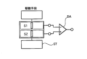
前記従来の差動型磁気センサは、図1に示されるように、距離L[m]離れた二つの地点の磁場H1、H2の環境におかれた検出感度が互いに等しい2つの磁気検知手段S1、S2と、この磁気検知手段から得られる磁場信号の差を求める差動演算手段DAとによって、2つの磁気検知手段から得られる磁場信号の差H1-H2を出力するものである。
しかしながら、たとえば直径0.1mmの鉄粉の磁場が1nTほどと極めて小さい磁場であるのに対して、ノイズとなる背景の磁場は、例えば、地磁気を例にとると数万nTとなり、測定目的の磁場に比べ非常に大きいものとなることもある。一方、これよりも低い磁場レベルである工場、作業場、実験室などのモータ、照明器具等から発せられる背景磁気ノイズでも、数百nT以上のこともあり、たとえば2つの磁気検知手段の感度差が1%であるとすると、差動演算の結果、すなわち前記H1-H2に相当する残留磁場成分が数nT相当の背景磁場として残ってしまい、前記鉄粉による磁場成分の1nTと区別ができないという不都合が生じる。そして、これにより大きい背景磁場の場合には、さらに感度差の影響が大きくなる。従って、このような局所的に存在する微弱磁場を精度よく抽出するためには、2つの磁気検知手段の検出感度の差が極力小さくなるようにし、理想的にはほぼ一致させる必要があり、2つの磁気信号が差動演算手段に入力されるまでに精確に検出感度を合わせておく必要がある。
このため従来においては、2つの磁気検知手段の特性が互いに一致するようにインライン検査をしながら製作するか、あるいは複数製作した中から特性の一致するものを選択して用いるという手法がとられてきたが、このような手法は工数および時間が増加することから、製作費用が高額になるという問題があった。
本発明者らは上記課題を解決し、高感度差動型磁気センサを安価に製作可能とするために、磁気インピーダンスセンサに信号調整手段を付加することによって、前記磁気インピーダンス素子の感度特性にばらつきによる差があっても検出された磁場信号電圧が差動演算手段に入力されるまでの間において調整され、2つの磁気検知手段の検出感度を極力等しいと見做せるように調整するという本発明の第1の技術的思想に着眼したものである。
本発明者らは、さらに検出感度の異なる前記2つの磁気インピーダンスセンサの検出感度の差異に対応して、信号調整手段により駆動手段から供給される駆動電流を調整するという本発明の第2の技術的思想に着眼するとともに、信号調整手段により2つの磁気インピーダンス素子に接続される信号処理手段の利得を調整するという本発明の第3の技術的思想に着眼した。
すなわち、前記した通り、差動型磁気センサで鉄粉等の局所的な微小磁場を測定しようとすると、2つの磁気インピーダンス素子の検出感度をほぼ一致させる必要があるが、実際には、製造上のばらつき等により、同じ検出感度の磁気インピーダンス素子を提供しようとしても、結果的に検出感度に差が生じてしまう場合がある。本発明では、このような場合でも信号調整手段を設けて、前記検出感度の差に応じて駆動電流または信号処理手段の利得が調整されることにより、局所的な微小磁場を精度良く測定可能とすることができる。
すなわち、前記した通り、差動型磁気センサで鉄粉等の局所的な微小磁場を測定しようとすると、2つの磁気インピーダンス素子の検出感度をほぼ一致させる必要があるが、実際には、製造上のばらつき等により、同じ検出感度の磁気インピーダンス素子を提供しようとしても、結果的に検出感度に差が生じてしまう場合がある。本発明では、このような場合でも信号調整手段を設けて、前記検出感度の差に応じて駆動電流または信号処理手段の利得が調整されることにより、局所的な微小磁場を精度良く測定可能とすることができる。
以上の検討の結果得られた本発明(請求項1に記載の第1発明)の差動型磁気センサは、
駆動電流を出力する駆動手段と、離れた2つの地点に配設された前記駆動電流が印加される2つの感磁体より成る2つの磁気インピーダンス素子を備え、前記感磁体の周辺の磁場強さに対応する磁場信号電圧を出力する2つの磁気検知手段と、
前記2つの磁気検知手段から出力される2つの磁場信号電圧の差を演算することにより、前記2つの地点の磁場の強さの差の信号を出力する差動演算手段とから成る差動型磁気センサにおいて、
前記駆動手段と前記差動演算手段との間に設けられ、検出感度の異なる前記2つの磁気インピーダンス素子を備えた前記2つの磁気検知手段が、周辺の磁場強さが同じであれば同じレベルの磁場信号電圧を出力するように出力信号を調整する信号調整手段を備えているものである。
駆動電流を出力する駆動手段と、離れた2つの地点に配設された前記駆動電流が印加される2つの感磁体より成る2つの磁気インピーダンス素子を備え、前記感磁体の周辺の磁場強さに対応する磁場信号電圧を出力する2つの磁気検知手段と、
前記2つの磁気検知手段から出力される2つの磁場信号電圧の差を演算することにより、前記2つの地点の磁場の強さの差の信号を出力する差動演算手段とから成る差動型磁気センサにおいて、
前記駆動手段と前記差動演算手段との間に設けられ、検出感度の異なる前記2つの磁気インピーダンス素子を備えた前記2つの磁気検知手段が、周辺の磁場強さが同じであれば同じレベルの磁場信号電圧を出力するように出力信号を調整する信号調整手段を備えているものである。
本発明(請求項2に記載の第2発明)の差動型磁気センサは、
前記第1発明において、
前記信号調整手段として、前記2つの磁気インピーダンス素子を構成する前記感磁体の検出感度の差異に対応して、前記駆動手段から供給される前記駆動電流が調整されるように構成されているものである。
前記第1発明において、
前記信号調整手段として、前記2つの磁気インピーダンス素子を構成する前記感磁体の検出感度の差異に対応して、前記駆動手段から供給される前記駆動電流が調整されるように構成されているものである。
本発明(請求項3に記載の第3発明)の差動型磁気センサは、
前記第1発明において、
前記信号調整手段として、前記2つの磁気インピーダンスセンサを構成する前記感磁体の検出感度の差異に対応して、前記2つの磁気インピーダンス素子に接続される前記磁気検知手段を構成する信号処理手段の利得が調整されるように構成されているものである。
前記第1発明において、
前記信号調整手段として、前記2つの磁気インピーダンスセンサを構成する前記感磁体の検出感度の差異に対応して、前記2つの磁気インピーダンス素子に接続される前記磁気検知手段を構成する信号処理手段の利得が調整されるように構成されているものである。
上記構成より成る第1発明の差動型磁気センサは、駆動電流を出力する駆動手段と、離れた2つの地点に配設された前記駆動電流が印加される2つの感磁体より成る2つの磁気インピーダンス素子を備え、前記感磁体の周辺の磁場強さに対応する磁場信号電圧を出力する2つの磁気検知手段と、前記2つの磁気検知手段から出力される2つの磁場信号電圧の差を演算することにより、前記2つの地点の磁場の強さの差の信号を出力する差動演算手段とから成る差動型磁気センサにおいて、前記駆動手段と前記差動演算手段との間に設けられた前記信号調整手段が、検出感度の異なる前記2つの磁気インピーダンス素子を備えた前記2つの磁気検知手段が周辺の磁場強さが同じであれば同じレベルの磁場信号電圧を出力するように出力信号を調整し、互いに磁気検知手段の検出感度が略同じであると見做せるような出力信号を出力するので、前記2つの地点共通の背景磁場成分を消去して、局所的な微弱磁場の検出を可能にするという効果を奏する。
上記構成より成る第2発明の差動型磁気センサは、前記第1発明における前記信号調整手段として、前記2つの磁気インピーダンス素子を構成する前記感磁体の検出感度の差異に対応して、前記駆動手段から供給される前記駆動電流が調整されるように構成されていることにより、前記2つの磁気インピーダンス素子が検出感度が異なっていても前記アモルファスワイヤの周辺の磁場強さに対応する磁場信号電圧を出力する際に、互いに検出感度が略同じとなるような磁場信号電圧に調整されて出力されるため、前記2つの地点共通の背景磁場成分を消去して、局所的な微弱磁場の精確な検出を可能にするという効果を奏する。
上記構成より成る第3発明の差動型磁気センサは、前記信号調整手段が、前記2つの磁気インピーダンス素子を構成する前記感磁体の検出感度の差異に対応して、前記2つの磁気インピーダンス素子に接続される前記それぞれの信号処理手段の利得が調整されるように構成されているので、検出感度が異なる前記2つの磁気インピーダンス素子を用いても、前記差動演算手段へ入力するまでの間に互いに略同一の感度となるように前記信号処理手段の利得を調整することができるので、前記2つの地点共通の背景磁場成分を消去して、局所的な微弱磁場の精確な検出を可能にするという効果を奏する。
以下、本発明の最良の実施の形態について、実施形態および実施例に基づき、図面を用いて説明する。
本第1実施形態の差動型磁気センサは、図2に示される様に2つの感磁体としてのアモルファスワイヤを備える磁気インピーダンス素子を含む2つの磁気検知手段S1およびS2と差動演算手段DAからなり、異なる2つの地点の磁場の差の信号を出力する差動型磁気センサにおいて、前記磁気検知手段S1およびS2と差動演算手段DAとの間に前記2つの磁気インピーダンス素子の前記アモルファスワイヤの検出感度の差に応じて周辺の磁場強さが同じであれば同じ大きさの磁場信号電圧が出力されるように出力信号を調整する信号調整手段STを設けるものである。
上記構成より成る第1実施形態の差動型磁気センサは、前記信号調整手段STが前記2つの磁気インピーダンス素子の検出感度に応じて信号を調整するので、前記2つの磁気インピーダンス素子の間に仮に検出感度に差異があったとしても2つの磁気インピーダンス素子の周辺の磁場強さが同じであれば、同じ大きさの磁場信号電圧が出力されると見做せるように、信号電圧が調整される。従って、前記差動演算手段DAにより前記2つの地点共通の背景磁場成分を相殺して、局所的な微弱磁場の検出を可能にするという効果を奏する。
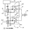
本第2実施形態の差動型磁気センサは、前記第1実施形態において、図3に示されるように前記2つの磁気インピーダンスセンサS1およびS2が、前記アモルファスワイヤより成る磁気インピーダンス素子E1およびE2とパルス電流を出力する駆動回路DCを含み、前記それぞれの磁気インピーダンス素子E1およびE2の検出感度とそれぞれの磁気インピーダンス素子に印加される駆動電流との積が互いに略等しくなるように前記磁気インピーダンス素子E1およびE2と前記駆動回路DCとの間に前記信号調整手段STとして抵抗回路r1およびr2を挿入するものである。
上記構成より成る第2実施形態の差動型磁気センサは、前記駆動回路DCに挿入された前記抵抗回路r1およびr2の抵抗値が、前記2つの磁気インピーダンス素子E1およびE2の検出感度の比率に応じた駆動電流が印加されるように設定されているので、前記2つの磁気インピーダンス素子E1およびE2の周辺の磁場強さに対応する交流電圧を検出コイルKC1およびKC2を介して出力するとともに前記駆動回路DCのもう一つのパルス出力によって動作するアナログスイッチAS11、AS21とコンデンサCh11、Ch21からなるサンプルホールド回路SH1、SH2により磁場信号に変換し、前記差動演算手段DAにより前記2つの地点共通の背景磁場成分を相殺して、微小鉄粉等に基づく局所的な微弱磁場の精確な検出を可能にするという効果を奏する。
本第3実施形態の差動型磁気センサは、図4に示されるように前記2つの磁気インピーダンスセンサS1およびS2は、増幅回路A1およびA2を含むサンプルホールド回路SH1およびSH2を含み、前記それぞれの感磁体より成る磁気インピーダンス素子E1およびE2の検出感度とそれぞれの磁気インピーダンス素子に接続される信号処理手段としてのサンプルホールド回路SH1およびSH2の利得との積が互いに略等しくなるように、前記信号調整手段STとして抵抗回路(図示せず)を挿入して前記サンプルホールド回路SH1およびSH2の前記増幅回路A1およびA2の増幅度が設定されているものである。
上記構成より成る第3実施形態の差動型磁気センサは、前記サンプルホールド回路SH1およびSH2の前記増幅回路A1およびA2の増幅度が、前記2つの磁気インピーダンス素子E1およびE2の検出感度の比率に応じて設定されているので、前記2つの磁気インピーダンス素子E1およびE2の周辺の磁場強さが同一であれば対応する磁場信号電圧に基づく増幅出力が同じ値と見做せるように調整され、前記差動演算手段DAに出力されることにより、前記差動演算手段DAの演算により前記2つの地点共通の背景磁場成分を相殺して、局所的な微小鉄粉等に基づく微弱磁場の精確な検出を可能にするという効果を奏する。
第1実施例の差動型磁気センサは、2つのアモルファスワイヤに通電する駆動電流を検出感度に応じて調整することにより、感度を一致させるもので、ある2点の外部磁場強さH1およびH2の差すなわち磁場の差(H1-H2)を計測する差動型磁気センサ、すなわち高感度磁気傾度計を構築するもので、本第1発明および第2発明に基づく実施例である。
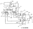
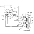
第1実施例の差動型磁気センサは、図5に示されるように検出コイル12および22が卷回された感磁体としての第1および第2のアモルファスワイヤ11および21と、2つのパルスP1およびP2を出力するパルス発振回路10と、2つの磁気インピーダンス素子E10およびE20を構成する前記第1および第2のアモルファスワイヤ11および21を駆動する駆動電流を出力する駆動回路2と、前記第1および第2のアモルファスワイヤ11および21の検出感度に応じた駆動電流に調整する信号調整回路3と、前記第1および第2の検出コイル21および22が出力する外部磁場信号をホールドする第1および第2のサンプルホールド回路41および42より成る信号処理手段4と、外部磁場の差(H1-H2)を演算する差動演算手段5とから成る。
前記感磁体を構成する前記アモルファスワイヤ11、21からなる2つの磁気インピーダンス素子E10、E20は、図5に示されるように距離Lだけ離して配置される。このLは、通常は0.01から10m程度のニーズが多いが、これ以外のニーズもある。
前記アモルファスワイヤ11は、外径10μm、長さ6mmのFeCoSiB系合金より成り、外部磁場H1が作用するある地点に配設され、一端は後述する直列に2個接続された抵抗r11、r21の一方の抵抗r11の一端に接続され、他端は、接地、周囲に検出コイル12が巻回されている。
前記アモルファスワイヤ21は、外径10μm、長さ6mmのFeCoSiB系合金より成り、前記ある地点からLメートル(m)離れた外部磁場H2が作用する点に配設され、一端は後述する直列に2個接続された抵抗r11,r21の他方の抵抗r21の一端に接続され、他端は接地され、周囲に検出コイル22が卷回されている。
パルス発振回路10(詳細図は省略)は、直列に接続された2個のロジック素子と抵抗およびコンデンサから成り、一定のパルス幅のパルス出力P1を出力する第1の出力端10Aと、該パルス出力P1のパルス幅より狭いパルスP2を同期させて出力する第2の出力端10Bを備えている。
駆動回路2は、所定の直流電流を出力する電圧源Eと、該電圧源Eのプラス端に一端が接続され、前記パルス発振回路11からのパルスP1が制御端に出力されている時に前記電圧源Eから出力される直流電流を供給するように制御する電子スイッチDSとから成る。
前記信号調整回路3は、直列に接続された第1および第2の抵抗r11およびr21とから成り、該第1の抵抗r11と第2の抵抗r21との接続点rcが前記駆動回路2の前記電子スイッチDSの他端に接続され、前記電子スイッチDSの前記制御端に前記パルス出力P1が印加されている間は、前記接続点に電圧源Eからの直流電流が通電されるように構成されている。
前記第1の検出コイル12は、一端121が所定の直流電位の直流電源(図示せず)に接続され、他端122がサンプルホールド回路41のアナログスイッチAS11に接続され、両端の間に前記アモルファスワイヤ11が置かれている周囲の外部磁場H1に対応する交流電圧が発生し、出力するように構成されている。
前記第2の検出コイル22は、一端221が所定の直流電位の直流電源(図示せず)に接続され、他端222がサンプルホールド回路のアナログスイッチAS21に接続され、前記両端221,222の間に前記アモルファスワイヤ21に前記信号調整回路3の前記第2の抵抗r21を介して駆動電流が印加されている時に、前記アモルファスワイヤ21が置かれている周囲の外部磁場H2に対応する交流電圧が発生し、出力するように構成されている。
前記信号処理手段4は、図5に示されるように前記第1の検出コイルに接続された第1のサンプルホールド回路41と前記第2の検出コイルに接続された第2のサンプルホールド回路42とから成る。
前記第1のサンプルホールド回路41は、前記第1の検出コイル12の前記他端122に一端が接続されるとともに、制御端が前記パルス発振回路10の第2の出力端10Bに接続された第1のアナログスイッチAS11と、該第1のアナログスイッチAS11の他端に一端が接続されるとともに、他端が前記直流電源(図示せず)に接続されたホールドコンデンサCh11とから成り、前記アナログスイッチAS11の他端に接続され、ホールドされた磁場H1に対応する電圧を増幅して出力する第1の緩衝増幅器A11を備えている。
前記第2のサンプルホールド回路42は、前記第2の検出コイル22の前記他端222に一端が接続されるとともに、制御端が前記パルス発振回路10の前記第2の出力端10Bに接続された第2のアナログスイッチAS21と、該第2のアナログスイッチAS21の他端に一端が接続されるとともに、他端が前記直流電源(図示せず)に接続されたホールドコンデンサCh21とから成り、前記アナログスイッチAS21の他端に接続され、ホールドされた磁場H2に対応する電圧を増幅して出力する第2の緩衝増幅器A21を備えている。
前記差動演算手段5は、前記第1の緩衝増幅器A11の出力端P11にプラス入力端が接続されるとともに、前記第2の緩衝増幅器A21の出力端P21にマイナス入力端が接続され、前記第1および第2の緩衝増幅回路A11およびA21からの出力電圧の差の電圧を出力する差動増幅器A31によって構成されている。
上記構成より成る第1実施例の差動型磁気センサにおける2つの磁気インピーダンスセンサの検出感度の調整について説明する。
前記アモルファスワイヤ11、21と前記検出コイル12、22からなる磁気インピーダンス素子E10、E20は、それぞれ製造過程においてばらつきが発生するので、磁気インピーダンス素子として組上げたときには、互いに検出感度における差を持つおそれがある。
前記アモルファスワイヤ11、21と前記検出コイル12、22からなる磁気インピーダンス素子E10、E20は、それぞれ製造過程においてばらつきが発生するので、磁気インピーダンス素子として組上げたときには、互いに検出感度における差を持つおそれがある。
たとえば前記パルスP1に基づき、前記アモルファスワイヤ11、21に所定の同じパルス電流を流したときの磁気インピーダンス素子としての検出感度をk1、k2とすると、両者の素子の感度に差異がある場合には通常以下の数1に示されるように検出感度k1とk2は同じ値にならなくなる。
(数1)
k1≠k2
k1≠k2
したがって上記2つの磁気インピーダンス素子を同一の基準となる磁場環境H0においたときの前記緩衝増幅器A11、A21の利得を1とすると出力端子P11、P21のそれぞれの出力H0×k1およびH0×k2は、以下の数2に示されるように同じ出力にはならない。製造上のばらつきによる検出感度の差異は微差のことが多く、大きな差異となることは少ないかもしれないが、前記した用途のように、例えば数nTレベルの非常に微小な鉄粉の磁場を測定しようとする場合には、このような検出感度の違いは、致命的な精度低下の原因となる。
(数2)
H0×k1≠H0×k2
H0×k1≠H0×k2
すなわち前記出力端子P11、P21は、前記差動演算手段5としての差動増幅器A31の入力端子を兼ねているので、該差動演算手段5の入力端子における2つの磁気検知手段の出力が異なるということであり、精確な磁場検出を可能にする差動型磁気センサとはならないため、検出感度の調整が必要になる。
前記2つの磁気インピーダンス素子の検出感度k1、k2は、前記パルスP1にもとづいて前記駆動回路2による前記アモルファスワイヤ11、21に流される電流の大きさに略比例するので、前記2つのアモルファスワイヤ11、21に流す電流を調整することにより、磁気インピーダンス素子としての検出感度の調整をすることができることになる。
すなわち前記2つの磁気検知手段の検出感度を同一にするには、検出感度の低い側の磁気インピーダンス素子のアモルファスワイヤに対してより大きなパルス電流を流すようにするか、または検出感度の高い側のアモルファスワイヤに対するパルス電流を減らすことで達成できるのである。
すなわち各アモルファスワイヤ11、12に流すパルス電流を、以下の数3に示される関係が成立するパルス電流i11、i21とすることにより、2つの磁気インピーダンス素子の検出感度を実質的に同一にすることができるのである。
(数3)
H0×k1×i11=H0×k2×i21
H0×k1×i11=H0×k2×i21
上記の式を整理すると、以下の数4に示されるようになる。すなわちこれが、2つの磁気インピーダンス素子の検出感度とそれぞれの磁気インピーダンス素子の駆動電流との積を互いに略等しくすることによって、検出感度を実質的に同一にする技術的原理である。
(数4)
k1×i11=k2×i21
k1×i11=k2×i21
前記2つのアモルファスワイヤ11、12に流れるパルス電流i11、i21は、2つのアモルファスワイヤの抵抗値をw11、w21および駆動回路2の電源Eの電圧をEdとすると、以下の数5および数6のようになる。なお、以下抵抗器の説明として記載するr21、r22等は、抵抗器の記号と抵抗値の両方を兼ねる意味で記載する。
(数5)
i11=Ed/(r11+w11)
i11=Ed/(r11+w11)
(数6)
i21=Ed/(r21+w21)
i21=Ed/(r21+w21)
上記数5および数6を、上述の数4に適用すると、以下の数7が得られる。
(数7)
r21=k2/k1(r11+w11)-w21
r21=k2/k1(r11+w11)-w21
すなわち、一方の磁気インピーダンス素子に所望の検出感度を与えるための駆動電流を印加することが出来る抵抗値の抵抗器r11を決定し、もう一方の磁気インピーダンス素子にこれと同じ感度を得るための抵抗器r21の抵抗値を上記数7により決定して、前記信号調整手段3として前記駆動回路2に前記抵抗器r11、r21より成る抵抗回路を挿入して駆動電流を調整すればよいのである。これにより2つの磁気検知手段のトータルの検出感度を実質的に同一と見做せるように調整することができるのである。
上記構成より成り、上述の調整が成された第1実施例の差動型磁気センサは、2つの磁気検知手段としての前記2つの磁気インピーダンスセンサと1つの差動演算手段とからなり、各磁気インピーダンスセンサはそれぞれのアモルファスワイヤ11、21をパルス駆動するための共通のパルス発振回路10とアモルファスワイヤ駆動回路2を備えている。
すなわち前記パルス発振回路10は、互いに同期関係にある所定周期のパルスP1とP2を2つの出力端10Aおよび10Bより出力する。
前記駆動回路2において、電子スイッチDSはその制御端子が、前記パルス発振回路10の前記パルスP1を出力する出力端10Aに接続され、接点が開閉制御される。該電子スイッチDSの一方の接点電極は、前記電圧源Eに接続され、もう一方の接点電極は前記アモルファスワイヤ11、21に直列接続された抵抗器 r11、 r21にそれぞれ接続されていることから、これにより前記パルスP1のオンオフに対応して前記アモルファスワイヤ11、21に対して、それぞれパルス電流i11、i21が通電される。
前記駆動回路2において、電子スイッチDSはその制御端子が、前記パルス発振回路10の前記パルスP1を出力する出力端10Aに接続され、接点が開閉制御される。該電子スイッチDSの一方の接点電極は、前記電圧源Eに接続され、もう一方の接点電極は前記アモルファスワイヤ11、21に直列接続された抵抗器 r11、 r21にそれぞれ接続されていることから、これにより前記パルスP1のオンオフに対応して前記アモルファスワイヤ11、21に対して、それぞれパルス電流i11、i21が通電される。
このパルス電流により前記アモルファスワイヤ11、21は、磁気インピーダンス効果を発現し、前記検出コイル12、22の各端子間にそれぞれのアモルファスワイヤ11、21が置かれている周囲の外部磁場H1、H2に対応する交流電圧が発生する。
この交流電圧はアナログスイッチAS11、AS21とホールドコンデンサCh11、Ch21と緩衝増幅器A11、A21からなる2つのサンプルホールド回路41および42により、前記パルスP2に基づき所定のタイミングでそれぞれサンプルされ、前記ホールドコンデンサCh11、Ch21に電圧としてホールドされ、該緩衝増幅器A11、A21からそれぞれ出力される。
該緩衝増幅器A11、A21の各出力端子P11、P21から出力される出力は、前記磁場H1とH2に対応し、かつ、両者の検出感度が同じと見做せるような出力に調整された出力となっている。
該緩衝増幅器A11、A21の各出力端子P11、P21から出力される出力は、前記磁場H1とH2に対応し、かつ、両者の検出感度が同じと見做せるような出力に調整された出力となっている。
よって第1実施例の差動型磁気センサは、前記差動演算手段5を構成する前記差動増幅器A31に入力されるまでの間に2つの磁気検知手段の検出感度を極力等しくするような出力に調整することができるので、従来のように同じ感度の磁気インピーダンス素子の組み合わせを探す工程も不要で、かつ生産した磁気インピーダンス素子をすべて有効に活用して、安価で微小鉄粉等の微弱磁場の高感度および高精度の検出を可能にするとともに、高感度・高精度の差動型磁気センサを実現することができるという作用効果を奏する。
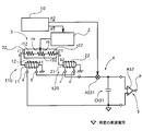
第2実施例の差動型磁気センサは、図6に示されるように上述の第1実施例の差動型磁気センサにおける前記信号調整手段3に対して、可変抵抗r32を付加するもので、以下相違点を中心に説明する。
前記信号調整手段において、電流調整を行う抵抗器の選択工程に可変抵抗器を用いる例であって、本第2実施例においては固定抵抗器r12、r22は同じ抵抗値とし、可変抵抗器r32の一方の電極と摺動子との間の抵抗値をra、もう一方の電極と摺動子との間の抵抗値をrbとすると、パルス電流i11、i21は以下の数8および数9のごとく設定できる。
(数8)
i11=Ed/(r12+ra+w11)
i11=Ed/(r12+ra+w11)
(数9)
i21=Ed/(r22+rb+w21)
i21=Ed/(r22+rb+w21)
この数8および数9を上記数4に適用すると、以下の数10を得ることが出来る。
(数10)
rb=k2/k1(r11+ra+w11)-(r21+w21)
rb=k2/k1(r11+ra+w11)-(r21+w21)
すなわち前記信号調整手段3として前記駆動回路2と前記アモルファスワイヤ11および21の間に抵抗r12、raおよびr22、rbによる抵抗回路32を介挿配設することで、2つの磁気検知手段のトータルの検出感度を実質的に同一と見做せるように調整することができるのである。
本第2実施例の差動型磁気センサは、前記可変抵抗器r32により抵抗値raおよびrbを連続的に高精度で設定ができるので、上述の第1実施例における固定抵抗器の取替え作業に比べて、感度を同一にするための工程の生産性をいちじるしく向上させることが出来るとともに、検査中に検出感度のバランスが変化しても、速やかに調整して対応出来るという作用効果を奏する。
本第2実施例においては、電子回路を簡略化する観点より磁気インピーダンス素子E10、E20の各検出コイル12、22を差動接続することにより、前記第1実施例における差動増幅器を省略するものである。
すなわち本第2実施例の差動型磁気センサは、各検出コイル12、22の巻終わり電極b、dを互いに接続して、巻き始め電極aとcの両電極間の電圧すなわち前記検出コイル12、22に生じる前記交流電圧の差の電圧を前記アナログスイッチAS31および前記ホールドコンデンサCh31から成り、前記緩衝増幅器を省略した1個のサンプルホールド回路のみによって、サンプルホールドすることにより、2つの磁場H1とH2との差の磁場信号を、緩衝増幅器を兼ねた差動演算手段5としての高入力インピーダンス増幅器A32の出力端子から出力するものであるので、電子回路を簡素化することにより、コストダウンを可能にして、精確な微弱磁場検出を可能にするという効果を奏する。
上記構成より成る第2実施例の差動型磁気センサは、高入力インピーダンス増幅器A32が、通常のOPアンプ(演算増幅器)を用いて高入力インピーダンス増幅回路を実現することも可能であり、高感度差動型磁気センサをより安価に実現するという作用効果を奏するものである。
本第3実施例の差動型磁気センサは、信号処理手段におけるサンプルホールド回路において利得調整する本第3発明に基づく実施例であり、以下上述した第1実施例との相違点を中心に説明する。
本第3実施例の差動型磁気センサは、前記した本第1実施例および第2実施例とは異なり、アモルファスワイヤに通電する駆動電流の調整によって、感度を調整するものではなく、図7に示すように前記2つのアモルファスワイヤ11、21は、従来の差動型磁気センサと同様に同じ抵抗値の抵抗器r0を介して同じパルス電流で駆動されている。従って、製造工程のばらつき等により、前記2つの磁気インピーダンス素子E10およびE20の検出感度が相違していた場合には、前記2つの磁気インピーダンス素子からの出力は互いに異なることとなる。
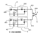
そこで、本第3実施例においては、磁気インピーダンス素子の検出感度の調整は前記信号処理手段4としての前記サンプルホールド回路に信号調整手段3としての抵抗回路331,332を挿入することにより、1以下の利得として減衰率を調整することにより行うものである。
より具体的には、緩衝増幅器としてOPアンプによる増幅度1のフォロワーA11、A21の出力端子と出力端子P11、P21との間に直列に接続された抵抗器r11、r12からなり、一端が直流電流源(図示せず)に接続され他端がフォロアーA11の出力端に接続されるとともに、抵抗器r11およびr12の接続点が前記出力端子P11に接続された第1の抵抗回路331と、直列に接続された抵抗r21、r22とからなり、一端が直流電流源(図示せず)に接続され他端がフォロアーA21の出力端子に接続されるとともに、抵抗器r21およびr22の接続点が前記出力端子P21に接続された第2の抵抗回路332をそれぞれ挿入するものである。
前記第1および第2の抵抗回路の減衰率は、
r11/(r11+r12)および
r21/(r21+r22)である。
r11/(r11+r12)および
r21/(r21+r22)である。
ここで前記2つの磁気インピーダンス素子E10およびE20の固有の検出感度をk1、k2とするとき、以下の数11に示されるように前記抵抗器r11、r12、r21、r22の抵抗値を設定することにより、前記差動演算手段5を構成する差動増幅器A33に入力されるまでの間に前記2つの磁気インピーダンス素子の検出感度が実質的に等しいと見做せるような出力信号に調整することができるのである。
(数11)
k1×r11/(r11+r12)=k2×r21/(r21+r22)
k1×r11/(r11+r12)=k2×r21/(r21+r22)
具体的には、以下の数12に示されるようであり、前記抵抗器r11、r12、r21の抵抗値をあらかじめ決定し、r22の抵抗値を下記数12に基づき算出して前記抵抗回路に適用するものである。
(数12)
r22=(k2×r21)/(k1×r11)×(r11+r12)-r21
r22=(k2×r21)/(k1×r11)×(r11+r12)-r21
なお前記抵抗r11、r21は、一例として緩衝増幅器A12、A21に対して大きな負荷とならない通常1kΩ以上とし、前記抵抗r12は抵抗r11との比において減衰率がたとえば10%程度となるようたとえば0.1kΩとした。 これは磁気インピーダンス素子の検出感度のばらつきが高々数%以内であるので、この範囲内で如何なるばらつきに対しても信号調整を可能にするr22の抵抗値の算出を可能にするためである。
なお前記抵抗器 r11、r12、r21、r22として可変抵抗器を採用することもできる。
なお前記抵抗器 r11、r12、r21、r22として可変抵抗器を採用することもできる。
上記構成より成る第3実施例の差動型磁気センサは、製造上のばらつき等により前記2つの磁気インピーダンス素子の検出感度に差異が生じた場合であっても、前記サンプルホールド回路41および42に介挿された信号調整手段としての第1および第2の抵抗回路331および332によって、前記差動演算手段5を構成する差動増幅器A33に入力される出力信号は、磁気検知手段の最終的な検出感度が実質的に同一になると見做せるような出力信号に調整することができるので、前記2つの地点共通の背景磁場成分を相殺して、検出すべき微小鉄粉等に基づく局所的な微弱磁場の精確な検出を可能にするという効果を奏する。
第4実施例の差動型磁気センサは、低価格化を可能にするために、図8に要部が示されるように、上述の第3実施例における差動演算手段5に対応するものとして、高入力インピーダンスの差動増幅器A34を用いることと、信号処理手段4としてのサンプルホールド回路41および42の緩衝増幅器A11、A21を省略したものであり、以下相違点を中心に説明する。
前記サンプルホールド回路41および42のホールドコンデンサCh1、Ch2と前記差動演算手段5としての高入力インピーダンス差動増幅器A34の入力端子P11、P21との間に、前記信号調整手段3として挿入する抵抗器r11、 r12および抵抗r21、r22からなる抵抗回路331および332による減衰回路を挿入するものである。
ここで 2つの磁気インピーダンス素子の検出感度を同一にする条件は、図7と同様であり既に記載した数12に基づいてr22を算出する。
ここで抵抗器r11、r21とサンプルホールド回路41および42のホールドコンデンサCh1、Ch2との積で決まる放電時定数t1、t2は、以下の数13および数14のようになる。
(数13)
t1=(r11+r12)×Ch1≒r11×Ch1 ∵ r11≫r12
t1=(r11+r12)×Ch1≒r11×Ch1 ∵ r11≫r12
(数14)
t2=(r21+r22)×Ch2≒r21×Ch2 ∵r21≫r22
t2=(r21+r22)×Ch2≒r21×Ch2 ∵r21≫r22
前記パルス発振回路10から出力される前記パルスP1、P2の周期をTとすると、前記サンプルホールド回路41および42による磁気信号の更新も周期Tで行われる。
上記放電時定数t1、t2がこの周期Tと同じか、それよりも大、すなわち以下の数15を満足するものであれば、サンプルホールドされたホールドコンデンサの電圧、すなわち検出した磁場信号を次の新たなサンプルホールドのタイミングまで所定の正確さで保持することができる。
上記放電時定数t1、t2がこの周期Tと同じか、それよりも大、すなわち以下の数15を満足するものであれば、サンプルホールドされたホールドコンデンサの電圧、すなわち検出した磁場信号を次の新たなサンプルホールドのタイミングまで所定の正確さで保持することができる。
(数15)
t1、t2≧ T
t1、t2≧ T
この場合に前記差動増幅器A34の入力インピーダンスが、前記抵抗器r11、 r21よりも十分高ければ、図7に示された前記緩衝増幅器A11、A21を省略することができるのである。
なお本第4実施例においては前記パルスP1、P2の繰り返し周期Tを1μs(マイクロ秒)、前記抵抗回路331、332によって構成される減衰回路の抵抗器の抵抗器r11、r21を、一例として300kΩ、コンデンサCh1、Ch2を100pF(ピコファラッド)に設定した。
この場合の前記放電時定数t1、t2は、以下の数16および数17のようになる。
(数16)
t1=r11×Ch1=300×103×100×10-12=30×10-6=30μs
t1=r11×Ch1=300×103×100×10-12=30×10-6=30μs
(数17)
t2=r21×Ch2=300×103×100×10-12=30×10-6=30μs
t2=r21×Ch2=300×103×100×10-12=30×10-6=30μs
よって前記放電時定数t1、t2は、ともにパルスP1、P2の周期T=1μsよりも十分大であり、前記数15が成り立ち、また通常の高入力インピーダンス増幅器の入力インピーダンスは、抵抗器r11、r21に用いた300kΩに比べて無視できるほど高いので、前記のごとく緩衝増幅器を省略できた。
なお前記信号調整手段3としての抵抗器r11とr12およびr21とr22からなる前記抵抗回路331および332より成る減衰回路により、2つの信号検知手段の感度を精確度高く調整できることは上記説明したとおりである。
以上から明らかな様に第4実施例の差動型磁気センサは、上述の第3実施例における緩衝増幅器としてのOPアンプのフォロワー回路を用いる必要がないので、さらなる低コスト化が実現できるという作用効果を奏する。
なお第3実施例と同様に前記抵抗器r11、r12、r21、r22として可変抵抗器を採用することができる。
なお第3実施例と同様に前記抵抗器r11、r12、r21、r22として可変抵抗器を採用することができる。
第5実施例の差動型磁気センサは、図9に示す通り、信号調整手段3としてサンプルホールド回路41および42の緩衝増幅器A12およびA22をOPアンプと抵抗回路351,352による非反転増幅器によって実現して差動演算器A35に出力するものである。
前記緩衝増幅器としてOPアンプA12、抵抗器r13、r14とOPアンプA22、抵抗器r23、r24からなる2つの非反転増幅器の利得は、以下のように設定できる。
(1+ r14/ r13)
(1+ r24/ r23)
(1+ r14/ r13)
(1+ r24/ r23)
したがって 前記2つの磁気インピーダンス素子の固有の感度をk1、k2とするとき、以下の数18となるように、抵抗器r13、r14、r23、r24の抵抗値を設定することにより、差動演算手段A35に入力されるまでの間に前記2つの磁気インピーダンス素子の検出感度を実質的に等しくなるように調整することができるのである。
(数18)
k1×(1+r14/r13)=k2×(1+r24/r23)
k1×(1+r14/r13)=k2×(1+r24/r23)
具体的には抵抗器r13、r14の抵抗値の設定によって、一方の磁気インピーダンス素子を所望の検出感度に設定し、もう一方の磁気インピーダンス素子の検出感度は抵抗r23=r13として数19によって算出したr24を適用する。
(数19)
r24=r23/k2×(k2-k1-k1×r14/r13)
なお前記抵抗器 r13、r14、r23、r24を可変抵抗器によって構成することができる。
r24=r23/k2×(k2-k1-k1×r14/r13)
なお前記抵抗器 r13、r14、r23、r24を可変抵抗器によって構成することができる。
上記構成より成る第5実施例の差動型磁気センサは、前記信号調整手段3として前記サンプルホールド回路41および42の緩衝増幅器A12およびA22をOPアンプと抵抗回路351,352による非反転増幅器によって実現して差動演算器A35に出力するものであるので、前記抵抗回路351および352の抵抗値を設定することにより、利得を1以上で増幅しながら実質的に磁気検知手段の最終的な検出感度が同一と見做せるような出力電圧を得ることができるため、より高感度な差動型磁気センサを実現するという作用効果を奏する。
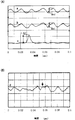
本第5実施例の差動型磁気センサを用いて、実際に磁場計測を行った計測例について、図10(A)を用いて以下に説明する。
すなわち2つの磁気検知手段の2つの磁気インピーダンスセンサ素子の距離を30mmとし、一方をベルトコンベアーにより通過する直径0.3mmの鉄粉の通過路近傍上部に、配設するとともに、もう一方をそれよりも上部にずらして配設して、計測を行ったものである。
すなわち2つの磁気検知手段の2つの磁気インピーダンスセンサ素子の距離を30mmとし、一方をベルトコンベアーにより通過する直径0.3mmの鉄粉の通過路近傍上部に、配設するとともに、もう一方をそれよりも上部にずらして配設して、計測を行ったものである。
上記計測の結果を示す図10(A)において、a、bは、各磁気検知手段の出力端子P11,P21からの出力の波形を示す。a、bは、ほぼ同等の波形であり、見やすくするため図10(A)においては上下にずらして表示している。
aの波形には鉄粉通過の微弱な磁気信号が含まれているが、ノイズとなる背景磁場成分がa、bともに最大で約80nT程度あるため、そのままでは微小な鉄粉通過時の磁気信号が、背景磁場成分に隠れてしまい、明確には視認できない。cは、前記差動演算器A35の差動演算の出力であり、差動演算効果により両出力の背景ノイズが約1/400に小さくなるとともにピーク値1.2nTの鉄粉通過による磁場変動波形を観察することができた。なお、cの波形は、磁場変動を見やすくするため、a、bに比べて縦軸のスケールを拡大して表示したものである。
なお、上記の計測実験では、地磁気が直流磁場であることを考慮し、低周波を除去するフィルタを用いて測定結果に影響が及ばないようにし、実験を行っている。
aの波形には鉄粉通過の微弱な磁気信号が含まれているが、ノイズとなる背景磁場成分がa、bともに最大で約80nT程度あるため、そのままでは微小な鉄粉通過時の磁気信号が、背景磁場成分に隠れてしまい、明確には視認できない。cは、前記差動演算器A35の差動演算の出力であり、差動演算効果により両出力の背景ノイズが約1/400に小さくなるとともにピーク値1.2nTの鉄粉通過による磁場変動波形を観察することができた。なお、cの波形は、磁場変動を見やすくするため、a、bに比べて縦軸のスケールを拡大して表示したものである。
なお、上記の計測実験では、地磁気が直流磁場であることを考慮し、低周波を除去するフィルタを用いて測定結果に影響が及ばないようにし、実験を行っている。
図10(B)に示される波形dは、本第5実施例の特徴である信号調整手段を適用せずに上記と同じ計測を行った比較例における差動演算後の出力波形である。この場合、背景ノイズが十分に小さくならず、それによって矢印で示した位置にみられるはずの鉄粉通過の波形が隠されてしまった例である。
上述の実施形態および実施例は、説明のために例示したもので、本発明としてはそれらに限定されるものではなく、特許請求の範囲、発明の詳細な説明および図面の記載から当業者が認識することができる本発明の技術的思想に反しない限り、変更および付加が可能である。
上述の実施形態および実施例においては、一例として感磁体としてアモルファスワイヤを採用したものについて説明したが、本発明としてはそれらに限定されるものではなく、感磁体として薄膜その他のものを必要に応じて採用することができるものである。
上述の実施形態および実施例においては、一例として感磁体としてのアモルファスワイヤの周囲に巻回した検出コイルによって外部磁場を検出する例について説明したが、本発明としてはそれらに限定されるものではなく、感磁体としてのアモルファスワイヤの両端の出力電圧によって外部磁場を検出する例を採用することができるものである。
上述の実施形態および実施例においては、一例として2つの磁気インピーダンス素子の検出感度の差に応じて、周辺の磁場強さが同じであれば同じ大きさの磁場信号電圧が出力されるように信号を調整する信号調整手段の例について説明したが、本発明としてはそれに限定されるものではなく、2つの磁気インピーダンス素子の検出感度の差を補うように信号を調整して、磁場信号電圧のレベルを等しくする信号調整手段や、2つの磁気検出手段のトータルの検知感度が等価と見做せるレベルの磁場信号電圧が出力されるように信号を調整する信号調整手段や、2つの磁気インピーダンス素子の検出感度に差があっても、2つの磁気検出手段の最終的な検知感度が等価であると仮定できるように、信号を調整する信号調整手段等を必要に応じて採用することができるものである。
理化学研究分野における微弱磁気検出、火山活動などによる地磁気その他の微小変動計測、複数の地点における磁場検出などの用途に好適である。
11、21 アモルファスワイヤ
10 パルス発振回路
2 駆動回路
3 信号調整手段
5 差動演算手段
12、22 検出コイル
41、42 サンプルホールド回路
10 パルス発振回路
2 駆動回路
3 信号調整手段
5 差動演算手段
12、22 検出コイル
41、42 サンプルホールド回路
Claims (3)
- 駆動電流を出力する駆動手段と、離れた2つの地点に配設された前記駆動電流が印加される2つの感磁体より成る2つの磁気インピーダンス素子を備え、前記感磁体の周辺の磁場強さに対応する磁場信号電圧を出力する2つの磁気検知手段と、
前記2つの磁気検知手段から出力される2つの磁場信号電圧の差を演算することにより、前記2つの地点の磁場の強さの差の信号を出力する差動演算手段とから成る差動型磁気センサにおいて、
前記駆動手段と前記差動演算手段との間に設けられ、検出感度の異なる前記2つの磁気インピーダンス素子を備えた前記2つの磁気検知手段が、周辺の磁場強さが同じであれば同じレベルの磁場信号電圧を出力するように出力信号を調整する信号調整手段を備えていることを特徴とする差動型磁気センサ。 - 前記請求項1において、
前記信号調整手段が、前記2つの磁気インピーダンス素子を構成する前記感磁体の検出感度の差異に対応して、前記駆動手段から供給される前記駆動電流が調整されるように構成されていることを特徴とする差動型磁気センサ。 - 前記請求項1において、
前記信号調整手段が、前記2つの磁気インピーダンス素子を構成する前記感磁体の検出感度の差異に対応して、前記2つの磁気インピーダンス素子に接続される前記磁気検知手段を構成する信号処理手段の利得が調整されるように構成されていることを特徴とする差動型磁気センサ。
Priority Applications (2)
| Application Number | Priority Date | Filing Date | Title |
|---|---|---|---|
| EP16771980.6A EP3264122B1 (en) | 2015-03-27 | 2016-02-23 | Differential magnetic sensor |
| US15/561,744 US10509080B2 (en) | 2015-03-27 | 2016-02-23 | Differential type magnetic sensor |
Applications Claiming Priority (2)
| Application Number | Priority Date | Filing Date | Title |
|---|---|---|---|
| JP2015066524A JP6414498B2 (ja) | 2015-03-27 | 2015-03-27 | 差動型磁気センサ |
| JP2015-066524 | 2015-03-27 |
Publications (1)
| Publication Number | Publication Date |
|---|---|
| WO2016158096A1 true WO2016158096A1 (ja) | 2016-10-06 |
Family
ID=57004157
Family Applications (1)
| Application Number | Title | Priority Date | Filing Date |
|---|---|---|---|
| PCT/JP2016/055247 Ceased WO2016158096A1 (ja) | 2015-03-27 | 2016-02-23 | 差動型磁気センサ |
Country Status (4)
| Country | Link |
|---|---|
| US (1) | US10509080B2 (ja) |
| EP (1) | EP3264122B1 (ja) |
| JP (1) | JP6414498B2 (ja) |
| WO (1) | WO2016158096A1 (ja) |
Cited By (3)
| Publication number | Priority date | Publication date | Assignee | Title |
|---|---|---|---|---|
| WO2019198603A1 (ja) * | 2018-04-12 | 2019-10-17 | 愛知製鋼株式会社 | 磁気計測システム、及び磁気センサの校正方法 |
| WO2019198602A1 (ja) * | 2018-04-12 | 2019-10-17 | 愛知製鋼株式会社 | マーカ検出システム、及びマーカ検出システムの運用方法 |
| WO2025182369A1 (ja) * | 2024-02-27 | 2025-09-04 | 愛知製鋼株式会社 | 磁気センサ装置 |
Families Citing this family (1)
| Publication number | Priority date | Publication date | Assignee | Title |
|---|---|---|---|---|
| JP6661570B2 (ja) * | 2017-05-11 | 2020-03-11 | 矢崎総業株式会社 | 磁界検出センサ |
Citations (3)
| Publication number | Priority date | Publication date | Assignee | Title |
|---|---|---|---|---|
| JPS59202057A (ja) * | 1983-04-30 | 1984-11-15 | Shimadzu Corp | 磁気探傷方法 |
| JPH1152036A (ja) * | 1997-08-04 | 1999-02-26 | Murata Mfg Co Ltd | 磁界検出素子の感度校正方法およびその感度校正方法を用いる磁界検出素子の感度校正装置 |
| JP2000098009A (ja) * | 1998-09-24 | 2000-04-07 | Koyo Electronics Ind Co Ltd | 磁気検出センサ |
Family Cites Families (13)
| Publication number | Priority date | Publication date | Assignee | Title |
|---|---|---|---|---|
| US2260589A (en) * | 1939-07-24 | 1941-10-28 | George S Smith | Magnetic flux meter |
| JP2566687B2 (ja) | 1991-03-27 | 1996-12-25 | 株式会社クボタ | トルク測定装置の温度補償装置 |
| JPH0980132A (ja) | 1995-09-18 | 1997-03-28 | Kokusai Denshin Denwa Co Ltd <Kdd> | 差動型交流磁気センサ |
| DE19615254C2 (de) * | 1996-04-18 | 1999-03-11 | Diagnostikforschung Inst | Gerät zur höchstempfindlichen magnetischen Detektion von Analyten |
| US6229307B1 (en) * | 1998-08-12 | 2001-05-08 | Minebea Co., Ltd. | Magnetic sensor |
| JP2002071770A (ja) * | 2000-08-31 | 2002-03-12 | Aichi Steel Works Ltd | 磁場検出装置 |
| DE10224747B4 (de) * | 2002-06-04 | 2004-05-13 | Infineon Technologies Ag | Sensorschaltung und Verfahren zur Herstellung derselben |
| JP2004301545A (ja) | 2003-03-28 | 2004-10-28 | Seiko Instruments Inc | 高分解能差動型磁気センサ及びその駆動装置 |
| WO2005033716A1 (en) * | 2003-10-01 | 2005-04-14 | Eaton Corporation | System and method for current sensing using anti-differential, error correcting current sensing |
| CN102822685B (zh) * | 2010-03-26 | 2014-11-05 | 佳能电子株式会社 | 检测由电流产生的磁场来估计电流量的方法 |
| US20120249126A1 (en) | 2011-03-31 | 2012-10-04 | Allegro Microsystems, Inc. | Circuits and methods for motion detection |
| JP2014190774A (ja) | 2013-03-26 | 2014-10-06 | Nagoya Univ | 磁気計測装置 |
| JP6163874B2 (ja) * | 2013-05-23 | 2017-07-19 | 株式会社リコー | 回転角度検出装置、画像処理装置及び回転角度検出方法 |
-
2015
- 2015-03-27 JP JP2015066524A patent/JP6414498B2/ja not_active Ceased
-
2016
- 2016-02-23 US US15/561,744 patent/US10509080B2/en active Active
- 2016-02-23 EP EP16771980.6A patent/EP3264122B1/en active Active
- 2016-02-23 WO PCT/JP2016/055247 patent/WO2016158096A1/ja not_active Ceased
Patent Citations (3)
| Publication number | Priority date | Publication date | Assignee | Title |
|---|---|---|---|---|
| JPS59202057A (ja) * | 1983-04-30 | 1984-11-15 | Shimadzu Corp | 磁気探傷方法 |
| JPH1152036A (ja) * | 1997-08-04 | 1999-02-26 | Murata Mfg Co Ltd | 磁界検出素子の感度校正方法およびその感度校正方法を用いる磁界検出素子の感度校正装置 |
| JP2000098009A (ja) * | 1998-09-24 | 2000-04-07 | Koyo Electronics Ind Co Ltd | 磁気検出センサ |
Non-Patent Citations (1)
| Title |
|---|
| See also references of EP3264122A4 * |
Cited By (5)
| Publication number | Priority date | Publication date | Assignee | Title |
|---|---|---|---|---|
| WO2019198603A1 (ja) * | 2018-04-12 | 2019-10-17 | 愛知製鋼株式会社 | 磁気計測システム、及び磁気センサの校正方法 |
| WO2019198602A1 (ja) * | 2018-04-12 | 2019-10-17 | 愛知製鋼株式会社 | マーカ検出システム、及びマーカ検出システムの運用方法 |
| US11143731B2 (en) | 2018-04-12 | 2021-10-12 | Aichi Steel Corporation | Magnetic measurement system and method of calibrating magnetic sensor |
| US12038757B2 (en) | 2018-04-12 | 2024-07-16 | Aichi Steel Corporation | Marker detection system and method of operating marker detection system |
| WO2025182369A1 (ja) * | 2024-02-27 | 2025-09-04 | 愛知製鋼株式会社 | 磁気センサ装置 |
Also Published As
| Publication number | Publication date |
|---|---|
| JP6414498B2 (ja) | 2018-10-31 |
| EP3264122B1 (en) | 2020-04-01 |
| US20180106872A1 (en) | 2018-04-19 |
| US10509080B2 (en) | 2019-12-17 |
| EP3264122A4 (en) | 2018-12-05 |
| JP2016186451A (ja) | 2016-10-27 |
| EP3264122A1 (en) | 2018-01-03 |
Similar Documents
| Publication | Publication Date | Title |
|---|---|---|
| Devices | Analog Devices | |
| KR100566547B1 (ko) | 자기검출기 | |
| US9739849B2 (en) | Magnetic field detecting device | |
| JP6414498B2 (ja) | 差動型磁気センサ | |
| JP2011528109A (ja) | 流動媒体の導電率を誘電測定する入力回路 | |
| CN103412009B (zh) | 一种测量流体电导率的装置和方法 | |
| US10345419B2 (en) | On-line calibration and compensation of a current transformer | |
| JP5811210B2 (ja) | 磁気検出器 | |
| JP5116433B2 (ja) | 変動磁場検出用磁気検出器 | |
| JP2009186433A (ja) | 渦電流式試料測定方法と、渦電流センサと、渦電流式試料測定システム | |
| JP2017062122A (ja) | 磁界検出装置 | |
| US9372217B2 (en) | Cable detector | |
| CN104040362A (zh) | 电流传感器 | |
| JP6952986B2 (ja) | 勾配磁界センサ | |
| JP4961623B2 (ja) | 磁気センサ | |
| EP3255445B1 (en) | Magneto-impedance (mi) magnetic sensor | |
| EP2230523A1 (en) | Physical quantity measuring unit and device for measuring a voltage and an electric field | |
| JP6460079B2 (ja) | Mi磁気センサ | |
| JP2020183878A (ja) | 高速高感度磁気センサ | |
| Petinrin et al. | Development of a Multi-Range Microcontroller Based Lock-In Digital Milliohm Meter | |
| RU2229141C1 (ru) | Измеритель параметров двухполюсников | |
| JP2020041945A (ja) | 磁界検出センサ | |
| EP3574334B1 (en) | A magnetic field sensor | |
| Riveros et al. | High sensitivity GMI gradiometer with an active interference compensation system | |
| EP3232210A1 (en) | Magnetic field sensor and apparatus for measuring magnetic field |
Legal Events
| Date | Code | Title | Description |
|---|---|---|---|
| 121 | Ep: the epo has been informed by wipo that ep was designated in this application |
Ref document number: 16771980 Country of ref document: EP Kind code of ref document: A1 |
|
| REEP | Request for entry into the european phase |
Ref document number: 2016771980 Country of ref document: EP |
|
| WWE | Wipo information: entry into national phase |
Ref document number: 15561744 Country of ref document: US |
|
| NENP | Non-entry into the national phase |
Ref country code: DE |