WO2016158483A1 - Élément d'imagerie à semi-conducteurs, procédé de commande et dispositif électronique - Google Patents
Élément d'imagerie à semi-conducteurs, procédé de commande et dispositif électronique Download PDFInfo
- Publication number
- WO2016158483A1 WO2016158483A1 PCT/JP2016/058648 JP2016058648W WO2016158483A1 WO 2016158483 A1 WO2016158483 A1 WO 2016158483A1 JP 2016058648 W JP2016058648 W JP 2016058648W WO 2016158483 A1 WO2016158483 A1 WO 2016158483A1
- Authority
- WO
- WIPO (PCT)
- Prior art keywords
- discharge
- unit
- photoelectric conversion
- pixel
- potential
- Prior art date
- Legal status (The legal status is an assumption and is not a legal conclusion. Google has not performed a legal analysis and makes no representation as to the accuracy of the status listed.)
- Ceased
Links
Images











Classifications
-
- H—ELECTRICITY
- H04—ELECTRIC COMMUNICATION TECHNIQUE
- H04N—PICTORIAL COMMUNICATION, e.g. TELEVISION
- H04N25/00—Circuitry of solid-state image sensors [SSIS]; Control thereof
- H04N25/60—Noise processing, e.g. detecting, correcting, reducing or removing noise
- H04N25/65—Noise processing, e.g. detecting, correcting, reducing or removing noise applied to reset noise, e.g. KTC noise related to CMOS structures by techniques other than CDS
-
- H—ELECTRICITY
- H04—ELECTRIC COMMUNICATION TECHNIQUE
- H04N—PICTORIAL COMMUNICATION, e.g. TELEVISION
- H04N25/00—Circuitry of solid-state image sensors [SSIS]; Control thereof
- H04N25/60—Noise processing, e.g. detecting, correcting, reducing or removing noise
- H04N25/616—Noise processing, e.g. detecting, correcting, reducing or removing noise involving a correlated sampling function, e.g. correlated double sampling [CDS] or triple sampling
-
- H—ELECTRICITY
- H04—ELECTRIC COMMUNICATION TECHNIQUE
- H04N—PICTORIAL COMMUNICATION, e.g. TELEVISION
- H04N25/00—Circuitry of solid-state image sensors [SSIS]; Control thereof
- H04N25/60—Noise processing, e.g. detecting, correcting, reducing or removing noise
- H04N25/62—Detection or reduction of noise due to excess charges produced by the exposure, e.g. smear, blooming, ghost image, crosstalk or leakage between pixels
- H04N25/621—Detection or reduction of noise due to excess charges produced by the exposure, e.g. smear, blooming, ghost image, crosstalk or leakage between pixels for the control of blooming
- H04N25/622—Detection or reduction of noise due to excess charges produced by the exposure, e.g. smear, blooming, ghost image, crosstalk or leakage between pixels for the control of blooming by controlling anti-blooming drains
-
- H—ELECTRICITY
- H04—ELECTRIC COMMUNICATION TECHNIQUE
- H04N—PICTORIAL COMMUNICATION, e.g. TELEVISION
- H04N25/00—Circuitry of solid-state image sensors [SSIS]; Control thereof
- H04N25/60—Noise processing, e.g. detecting, correcting, reducing or removing noise
- H04N25/62—Detection or reduction of noise due to excess charges produced by the exposure, e.g. smear, blooming, ghost image, crosstalk or leakage between pixels
- H04N25/621—Detection or reduction of noise due to excess charges produced by the exposure, e.g. smear, blooming, ghost image, crosstalk or leakage between pixels for the control of blooming
- H04N25/623—Detection or reduction of noise due to excess charges produced by the exposure, e.g. smear, blooming, ghost image, crosstalk or leakage between pixels for the control of blooming by evacuation via the output or reset lines
-
- H—ELECTRICITY
- H04—ELECTRIC COMMUNICATION TECHNIQUE
- H04N—PICTORIAL COMMUNICATION, e.g. TELEVISION
- H04N25/00—Circuitry of solid-state image sensors [SSIS]; Control thereof
- H04N25/60—Noise processing, e.g. detecting, correcting, reducing or removing noise
- H04N25/62—Detection or reduction of noise due to excess charges produced by the exposure, e.g. smear, blooming, ghost image, crosstalk or leakage between pixels
- H04N25/626—Reduction of noise due to residual charges remaining after image readout, e.g. to remove ghost images or afterimages
-
- H—ELECTRICITY
- H04—ELECTRIC COMMUNICATION TECHNIQUE
- H04N—PICTORIAL COMMUNICATION, e.g. TELEVISION
- H04N25/00—Circuitry of solid-state image sensors [SSIS]; Control thereof
- H04N25/70—SSIS architectures; Circuits associated therewith
- H04N25/76—Addressed sensors, e.g. MOS or CMOS sensors
- H04N25/77—Pixel circuitry, e.g. memories, A/D converters, pixel amplifiers, shared circuits or shared components
-
- H—ELECTRICITY
- H04—ELECTRIC COMMUNICATION TECHNIQUE
- H04N—PICTORIAL COMMUNICATION, e.g. TELEVISION
- H04N25/00—Circuitry of solid-state image sensors [SSIS]; Control thereof
- H04N25/70—SSIS architectures; Circuits associated therewith
- H04N25/76—Addressed sensors, e.g. MOS or CMOS sensors
- H04N25/77—Pixel circuitry, e.g. memories, A/D converters, pixel amplifiers, shared circuits or shared components
- H04N25/771—Pixel circuitry, e.g. memories, A/D converters, pixel amplifiers, shared circuits or shared components comprising storage means other than floating diffusion
-
- H—ELECTRICITY
- H10—SEMICONDUCTOR DEVICES; ELECTRIC SOLID-STATE DEVICES NOT OTHERWISE PROVIDED FOR
- H10F—INORGANIC SEMICONDUCTOR DEVICES SENSITIVE TO INFRARED RADIATION, LIGHT, ELECTROMAGNETIC RADIATION OF SHORTER WAVELENGTH OR CORPUSCULAR RADIATION
- H10F39/00—Integrated devices, or assemblies of multiple devices, comprising at least one element covered by group H10F30/00, e.g. radiation detectors comprising photodiode arrays
- H10F39/10—Integrated devices
- H10F39/12—Image sensors
- H10F39/18—Complementary metal-oxide-semiconductor [CMOS] image sensors; Photodiode array image sensors
-
- H—ELECTRICITY
- H10—SEMICONDUCTOR DEVICES; ELECTRIC SOLID-STATE DEVICES NOT OTHERWISE PROVIDED FOR
- H10F—INORGANIC SEMICONDUCTOR DEVICES SENSITIVE TO INFRARED RADIATION, LIGHT, ELECTROMAGNETIC RADIATION OF SHORTER WAVELENGTH OR CORPUSCULAR RADIATION
- H10F39/00—Integrated devices, or assemblies of multiple devices, comprising at least one element covered by group H10F30/00, e.g. radiation detectors comprising photodiode arrays
- H10F39/10—Integrated devices
- H10F39/12—Image sensors
- H10F39/18—Complementary metal-oxide-semiconductor [CMOS] image sensors; Photodiode array image sensors
- H10F39/186—Complementary metal-oxide-semiconductor [CMOS] image sensors; Photodiode array image sensors having arrangements for blooming suppression
- H10F39/1865—Overflow drain structures
-
- H—ELECTRICITY
- H10—SEMICONDUCTOR DEVICES; ELECTRIC SOLID-STATE DEVICES NOT OTHERWISE PROVIDED FOR
- H10F—INORGANIC SEMICONDUCTOR DEVICES SENSITIVE TO INFRARED RADIATION, LIGHT, ELECTROMAGNETIC RADIATION OF SHORTER WAVELENGTH OR CORPUSCULAR RADIATION
- H10F39/00—Integrated devices, or assemblies of multiple devices, comprising at least one element covered by group H10F30/00, e.g. radiation detectors comprising photodiode arrays
- H10F39/80—Constructional details of image sensors
- H10F39/802—Geometry or disposition of elements in pixels, e.g. address-lines or gate electrodes
-
- H—ELECTRICITY
- H10—SEMICONDUCTOR DEVICES; ELECTRIC SOLID-STATE DEVICES NOT OTHERWISE PROVIDED FOR
- H10F—INORGANIC SEMICONDUCTOR DEVICES SENSITIVE TO INFRARED RADIATION, LIGHT, ELECTROMAGNETIC RADIATION OF SHORTER WAVELENGTH OR CORPUSCULAR RADIATION
- H10F39/00—Integrated devices, or assemblies of multiple devices, comprising at least one element covered by group H10F30/00, e.g. radiation detectors comprising photodiode arrays
- H10F39/80—Constructional details of image sensors
- H10F39/803—Pixels having integrated switching, control, storage or amplification elements
- H10F39/8037—Pixels having integrated switching, control, storage or amplification elements the integrated elements comprising a transistor
- H10F39/80373—Pixels having integrated switching, control, storage or amplification elements the integrated elements comprising a transistor characterised by the gate of the transistor
-
- H—ELECTRICITY
- H10—SEMICONDUCTOR DEVICES; ELECTRIC SOLID-STATE DEVICES NOT OTHERWISE PROVIDED FOR
- H10F—INORGANIC SEMICONDUCTOR DEVICES SENSITIVE TO INFRARED RADIATION, LIGHT, ELECTROMAGNETIC RADIATION OF SHORTER WAVELENGTH OR CORPUSCULAR RADIATION
- H10F39/00—Integrated devices, or assemblies of multiple devices, comprising at least one element covered by group H10F30/00, e.g. radiation detectors comprising photodiode arrays
- H10F39/80—Constructional details of image sensors
- H10F39/813—Electronic components shared by multiple pixels, e.g. one amplifier shared by two pixels
Definitions
- the present disclosure relates to a solid-state imaging device, a driving method, and an electronic device, and particularly to a solid-state imaging device, a driving method, and an electronic device that can capture a higher quality image.
- a solid-state imaging device such as a CCD (Charge Coupled Device) or a CMOS (Complementary Metal Oxide Semiconductor) image sensor is used.
- the solid-state imaging device has a pixel in which a PD (photodiode) that performs photoelectric conversion and a plurality of transistors are combined, and outputs from a plurality of pixels arranged on an image plane on which a subject image is formed. An image is constructed based on the pixel signals to be processed.
- imaging is performed by a rolling shutter method in which charges generated in a PD are sequentially read for each row in which pixels are arranged.
- CMOS image sensor having a structure in which imaging is performed by the global shutter method
- the configuration suitable for capturing a moving image formed with a low potential of the overflow gate has not been a configuration suitable for capturing a still image. That is, in view of the entire imaging system, the potential of the overflow gate needs to be lowered, and as a result, the accumulated charge amount of the PD is reduced.
- Patent Document 1 a solid-state imaging device capable of switching the potential of the overflow gate between a still image and a moving image.
- the solid-state imaging device disclosed in Patent Document 1 has a configuration in which the potential of the overflow gate is switched by changing the potential of the overflow drain. There is a concern that the charge flows back to the PD. As described above, the charge flowing backward from the overflow drain to the PD may adversely affect the image quality, and the image quality is deteriorated.
- the present disclosure has been made in view of such a situation, and is capable of capturing a higher quality image.
- a solid-state imaging device includes a photoelectric conversion unit that converts incident light into electric charge by photoelectric conversion and accumulates, a discharge unit that discharges charge remaining in the photoelectric conversion unit, and the photoelectric conversion
- a driving method is a driving method of a solid-state imaging device, and the solid-state imaging device includes a photoelectric conversion unit that converts incident light into electric charge by photoelectric conversion and stores the charge, and a photoelectric conversion unit.
- a plurality of pixels having a discharge unit that discharges the remaining charge and a discharge drive unit that is driven when discharging the charge from the photoelectric conversion unit to the discharge unit; and at least two of the discharge drive units Is arranged in series between the photoelectric conversion unit and the discharge unit, and when performing a reset operation of the photoelectric conversion unit when starting exposure of the pixel at the time of capturing a still image,
- the potential of the discharge driving unit on the photoelectric conversion unit side is first set. Undo Then it performs driving to restore the potential of the other of the discharge driving unit.
- An electronic apparatus includes a photoelectric conversion unit that converts incident light into electric charge by photoelectric conversion and stores the charge, a discharge unit that discharges charge remaining in the photoelectric conversion unit, and the photoelectric conversion unit
- a plurality of pixels having a discharge drive unit that is driven when discharging electric charges from the discharge unit to the discharge unit, and at least two of the discharge drive units are connected in series between the photoelectric conversion unit and the discharge unit.
- a solid-state imaging device is provided.
- a photoelectric conversion unit that converts incident light into electric charge by photoelectric conversion and accumulates, a discharge unit that discharges charge remaining in the photoelectric conversion unit, and a photoelectric conversion unit to a discharge unit
- a plurality of pixels having a discharge drive unit that is driven when discharging electric charges are provided, and at least two or more discharge drive units are arranged in series between the photoelectric conversion unit and the discharge unit. Then, when performing the reset operation of the photoelectric conversion unit when starting exposure of the pixel during the still image capturing, the photoelectric conversion is performed by lowering the potentials of all the discharge drive units arranged in series. After discharging the electric charge remaining in the discharge unit to the discharge unit, the potential of the discharge drive unit on the photoelectric conversion unit side is first restored, and then the drive of returning the potential of the other discharge drive unit to the original is performed. Done.
- a higher quality image can be taken.
- FIG. 3 is a diagram illustrating a second layout example of the pixel 21.
- FIG. 6 is a diagram illustrating a third layout example of the pixel 21.
- FIG. 7 is a diagram illustrating a fourth layout example of the pixel 21.
- FIG. 11 is a diagram illustrating a fifth layout example of the pixel 21.
- FIG. 12 is a diagram illustrating a sixth layout example of the pixel 21.
- FIG. 11 is a diagram illustrating a seventh layout example of the pixel 21.
- FIG. 10 is a diagram illustrating an eighth layout example of the pixel 21.
- 10 is a diagram illustrating a ninth layout example of the pixel 21. It is a figure which shows the 10th layout example of the pixel. It is a block diagram showing an example of composition of an embodiment of an imaging device to which this art is applied. It is a figure which shows the usage example which uses an image sensor.
- FIG. 1 is a block diagram illustrating a configuration example of an embodiment of an image sensor to which the present technology is applied.
- the image sensor 11 includes a pixel region 12, a vertical drive circuit 13, a column signal processing circuit 14, a horizontal drive circuit 15, an output circuit 16, and a control circuit 17.
- the pixel region 12 is a light receiving surface that receives light collected by an optical system (not shown).
- a plurality of pixels 21 are arranged in a matrix in the pixel region 12, and each pixel 21 is connected to the vertical drive circuit 13 for each row via a horizontal signal line 22, and the vertical signal line 23 is connected to the pixel region 12.
- Each of the plurality of pixels 21 outputs a pixel signal at a level corresponding to the amount of light received, and an image of a subject that forms an image in the pixel region 12 is constructed from these pixel signals.
- the vertical drive circuit 13 sequentially outputs a drive signal for driving (transferring, selecting, resetting, etc.) each pixel 21 for each row of the plurality of pixels 21 arranged in the pixel region 12 and the horizontal signal line 22.
- the column signal processing circuit 14 performs CDS (Correlated Double Sampling) processing on the pixel signal output from the plurality of pixels 21 via the vertical signal line 23, thereby performing AD conversion of the pixel signal. And reset noise.
- CDS Correlated Double Sampling
- the horizontal driving circuit 15 sequentially outputs a driving signal for outputting a pixel signal from the column signal processing circuit 14 to the data output signal line 24 for each column of the plurality of pixels 21 arranged in the pixel region 12. 14.
- the output circuit 16 amplifies the pixel signal supplied from the column signal processing circuit 14 via the data output signal line 24 at a timing according to the driving signal of the horizontal driving circuit 15 and outputs the amplified pixel signal to the subsequent signal processing circuit.
- the control circuit 17 controls driving of each block by generating and supplying a clock signal according to the driving cycle of each block of the image sensor 11, for example.
- the image sensor 11 configured as described above is driven by a global shutter system that realizes the simultaneous accumulation of charges in all the pixels 21. As a result, the image sensor 11 can capture an image that does not generate distortion, for example, that occurs in imaging using a rolling shutter system.
- FIG. 2 is a circuit diagram showing a configuration example of the pixel 21.
- the pixel 21 includes a PD 31, a first transfer transistor 32, a memory unit 33, a second transfer transistor 34, an FD unit 35, an amplification transistor 36, a selection transistor 37, a reset transistor 38, and 2 Two discharge transistors 39-1 and 39-2 are provided.
- the PD 31 is a photoelectric conversion unit that converts incident light into electric charge by photoelectric conversion and accumulates it.
- the anode terminal is grounded and the cathode terminal is connected to the first transfer transistor 32 and the discharge transistor 39-1. ing.
- the first transfer transistor 32 is driven according to the transfer signal TRX supplied from the vertical drive circuit 13, and when the first transfer transistor 32 is turned on, the charge accumulated in the PD 31 is transferred to the memory unit 33.
- the memory unit 33 is a buried low-noise charge holding unit configured by implanting an N-type impurity into a P-well. Thus, the charge transferred from the PD 31 is temporarily held.
- the second transfer transistor 34 is driven according to the transfer signal TRG supplied from the vertical drive circuit 13, and when the second transfer transistor 34 is turned on, the charge accumulated in the memory unit 33 is transferred to the FD unit 35.
- the FD portion 35 is a floating diffusion region having a predetermined storage capacity connected to the gate electrode of the amplification transistor 36 and accumulates charges transferred from the memory portion 33.
- the amplification transistor 36 outputs a pixel signal of a level corresponding to the electric charge accumulated in the FD unit 35 (that is, the potential of the FD unit 35) to the vertical signal line 23 via the selection transistor 37.
- the FD unit 35 and the amplification transistor 36 serve as a conversion unit that converts the charge generated in the PD 31 into a pixel signal having a level corresponding to the charge. Function.
- the selection transistor 37 is driven according to the selection signal SEL supplied from the vertical drive circuit 13, and when the selection transistor 37 is turned on, the pixel signal output from the amplification transistor 36 can be output to the vertical signal line 23.
- the reset transistor 38 is driven in accordance with the reset signal RST supplied from the vertical drive circuit 13, and when the reset transistor 38 is turned on, the charge accumulated in the FD unit 35 is discharged to the reset power source Vrst, and the FD unit 35 is Reset.
- the discharge transistors 39-1 and 39-2 are arranged in series between the PD 31 and the overflow drain OFD (discharge unit). Further, the discharge transistor 39-1 is driven according to the discharge signal OFG1 supplied from the vertical drive circuit 13, and the discharge transistor 39-2 is driven according to the discharge signal OFG2 supplied from the vertical drive circuit 13. Therefore, when both the discharge transistors 39-1 and 39-2 are turned on, the charge accumulated in the PD 31 is discharged to the overflow drain OFD. In addition, the potentials of the discharge transistors 39-1 and 39-2 are set lower than the potential of the first transfer transistor 32 so that charges larger than the storage capacity generated in the PD 31 overflow into the overflow drain OFD.
- the exposure of the PD 31 is started. Such driving is performed.
- the PD 31 is formed by the PN junction of the N-type region 52 and the P-type region 53 formed in the P well of the semiconductor substrate 51.
- the memory unit 33 is formed by the N-type region 54 and the P-type region 55 that are formed in the adjacent region from the PD 31 via the first transfer transistor 32. Note that the memory unit 33 may be configured by only the N-type region 54 without forming the P-type region 55.
- the high-concentration N-type region 56 having a high N-type impurity concentration formed in the adjacent region from the memory unit 33 via the second transfer transistor 34 is connected to the gate electrode of the amplification transistor 36 through a wiring.
- An overflow drain OFD is connected to the high concentration N type region 57 having a high N type impurity concentration formed in the adjacent region from the PD 31 via the discharge transistors 39-1 and 39-2. .
- a gate electrode 61 of the first transfer transistor 32, a gate electrode 62 of the second transfer transistor 34, and a gate of the discharge transistor 39-1 are disposed through a gate insulating film (not shown).
- the electrode 63-1 and the gate electrode 63-2 of the discharge transistor 39-2 are stacked.
- the gate electrode 61 of the first transfer transistor 32 is formed so as to cover the region between the PD 31 and the memory unit 33 and the entire memory unit 33.
- the gate electrode 62 of the second transfer transistor 34 is formed so as to cover a region between the memory unit 33 and the high concentration N-type region 56.
- the gate electrode 63-1 of the discharge transistor 39-1 and the gate electrode 63-2 of the discharge transistor 39-2 are formed so as to cover the region between the PD 31 and the high concentration N-type region 57. As shown in the figure, the gate electrode 63-1 of the discharge transistor 39-1 is disposed on the PD 31 side, and the gate electrode 63-2 of the discharge transistor 39-2 is disposed on the high concentration N-type region 57 side. In this way, the gate electrode 63-1 of the discharge transistor 39-1 and the gate electrode 63-2 of the discharge transistor 39-2 are arranged in series from the PD 31 toward the high concentration N-type region 57.
- the pixel 21 configured as described above can transfer the charge generated in the PD 31 to the memory unit 33 and temporarily hold the charge in the memory unit 33 until the pixel signal of the pixel 21 is read. it can.
- exposure can be started simultaneously, and the transfer of charges from the PD 31 to the memory unit 33 can be performed simultaneously, so that the exposure can be ended simultaneously.
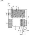
- FIG. 4 is a first layout example showing a planar configuration of the pixel 21.
- the PD 31 is arranged on the lower side and the memory unit 33 is arranged on the upper side.
- the memory unit 33 is covered with the gate electrode 61 of the first transfer transistor 32.
- a high-concentration N-type region 56 is disposed on the left side in FIG. 4 with respect to the memory unit 33 via the second transfer transistor 34.
- a wiring 71 for connecting to the gate electrode of the transistor 36 is connected.
- a high-concentration N-type region 57 is disposed on the right side in FIG. 4 with respect to the PD 31 via the discharge transistors 39-1 and 39-2. Further, in the pixel 21, the amplification transistor 36, the selection transistor 37, and the reset transistor 38 illustrated in FIG. 3 are provided on the opposite side (left side in FIG. 4) to the side where the high concentration N-type region 57 is disposed with respect to the PD 31. A pixel transistor region 72 is formed for formation.
- the pixel 21 has a structure in which the discharge transistors 39-1 and 39-2 are arranged in series between the PD 31 and the high-concentration N-type region 57. Further, the pixel 21 does not have to be arranged so that the discharge transistors 39-1 and 39-2 are adjacent to the memory unit 33. Further, the pixel 21 has a layout in which discharge transistors 39-1 and 39-2 are arranged with respect to the PD 31 on the side opposite to the side where the second transfer transistor 34 is arranged with respect to the memory unit 33. .
- the pixel 21 is configured, and an overflow that discharges charges from the PD 31 to the overflow drain OFD by a discharge signal OFG2 supplied to the discharge transistor 39-2 when capturing a still image and when capturing a moving image.
- the gate potential can be switched.
- the left side of FIG. 5 shows the potential of the pixel 21 when capturing a still image
- the right side of FIG. 5 shows the potential of the pixel 21 when capturing a moving image.
- the discharge signal OFG2 supplied to the discharge transistor 39-2 is always set to the Hi level. For this reason, the reset operation for discharging the charge remaining in the PD 31 is performed by driving only the discharge transistor 39-1 when capturing a moving image, and the discharge transistors 39-1 and 39 when capturing a still image. -2 is performed by driving both.
- the pixel 21 sets the discharge signal OFG2 supplied to the discharge transistor 39-2 at the time of capturing a moving image to the Hi level, thereby lowering the potential of the overflow gate as compared with the case of capturing a still image. be able to.
- the discharge signal OFG2 supplied to the discharge transistor 39-2 is set to Hi level, the potential below the discharge transistor 39-2 is lowered, and the potential below the discharge transistor 39-1 is lowered due to the modulation. Will do.
- the pixel 21 is configured to always set the discharge signal OFG2 to the Hi level to lower the potential of the overflow gate when capturing a moving image, and in particular to lower the potential of the first transfer transistor 32. ing.
- the pixel 21 is configured to increase the potential of the overflow gate by setting the discharge signals OFG1 and OFG2 to the low level when the PD 31 is exposed when capturing a still image.
- the potential of the overflow gate that causes the charge generated in the PD to overflow is adjusted by changing the potential of the overflow drain OFD. That is, the conventional pixel has a configuration in which the potential of the overflow gate is changed in response to the modulation of the potential of the overflow drain OFD.
- the interface state of the overflow gate may deteriorate over time.
- the pixel 21 is configured to adjust the potential of the overflow gate by switching the discharge signal OFG2 supplied to the discharge transistor 39-2 without changing the potential of the overflow drain OFD.
- the pixel 21 it is possible to suppress the aging deterioration of the interface state of the overflow gate, and it is possible to avoid a decrease in reliability.
- the pixel 21 can be prevented from appearing as a defective transfer defect, and deterioration in image quality can be avoided.
- the pixel 21 can be driven by a driving method that prevents the charge from being pumped up from the overflow drain OFD in the reset operation of the PD 31 that is performed when exposure is started.
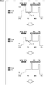
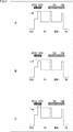
- 6 and 7 show a change in potential when the PD 31 is reset when the exposure of the pixel 21 is started when a still image is captured.
- the charge that becomes noise remains in the PD 31. That is, after the charge generated by the exposure one frame before is transferred from the PD 31 to the memory unit 33 (MEM), the charge photoelectrically converted by the PD 31 is accumulated. Therefore, in order to avoid the pixel signal being affected by this charge, a reset operation is performed to discharge the charge remaining in the PD 31 to the overflow drain OFD when the exposure is started.
- MEM memory unit 33
- the drive signal OFG1 supplied to the discharge transistor 39-1 is at a low level, and the drive signal OFG2 supplied to the discharge transistor 39-2 is at a low level. Yes.
- the potential below the discharge transistor 39-1 is set to be slightly lower than the potential below the first transfer transistor 32.
- the potential below the drain transistor 39-2 is set to be sufficiently lower than the potential below the first transfer transistor 32.
- the drive signal OFG1 supplied to the discharge transistor 39-1 is switched from the Low level to the Hi level, as shown in the third row (bottom row) from the top in FIG.
- the potential of the discharge transistor 39-1 becomes lower than the potential of the PD 31, and the charge accumulated in the PD 31 is discharged to the overflow drain OFD. That is, in the pixel 21, in a state where both the drive signals OFG1 and OFG2 are at the Hi level, the potential of the discharge transistor 39-1 is lower than the potential of the PD 31, and the potential of the discharge transistor 39-2 is the discharge transistor 39.
- Each potential is set to be lower than the potential of -1.
- the drive signal OFG1 supplied to the discharge transistor 39-1 is switched from the Hi level to the Low level, and the potential of the discharge transistor 39-1 is restored.
- the drive signal OFG2 supplied to the discharge transistor 39-2 is switched from the Hi level to the Low level, and the potential of the discharge transistor 39-2 is restored. Thereby, the reset operation of the PD 31 is completed, and the exposure of the PD 31 is started.
- the pixel 21 discharges the charge accumulated in the PD 31 at the time of capturing a still image, and then returns the potential of the discharge transistor 39-1 first, and then the potential of the discharge transistor 39-2. Driving is performed to restore the initial value. Thereby, in the pixel 21, it is possible to prevent the charge from being assembled from the overflow drain OFD.
- the overflow drain OFD when the overflow drain OFD is lowered in voltage, the charge may flow backward from the overflow drain OFD to the PD, and the pixel signal is saturated due to the charge leaked into the PD (white point) ). As a result, there is a concern that the image quality is deteriorated. As a result, it is impossible to expect an increase in the accumulated charge amount of PD as expected.
- the pixel 21 is driven by the driving method described with reference to FIGS. 6 and 7 to prevent the charge from flowing back to the PD 31 from the overflow drain OFD, resulting in a deterioration in image quality. You can avoid that.
- both the drive signals OFG1 and OFG2 are set to Hi at the same timing. You may drive so that it may become a level. Further, for example, as shown in FIG. 9, the driving signal OFG1 may be driven to the Hi level first, and then the driving signal OFG2 may be driven to the Hi level.
- the timing at which the drive signal OFG1 is set to the Hi level and the timing at which the drive signal OFG2 is set to the Hi level are in any order. May be.
- FIG. 10 shows a change in potential when the PD 31 is reset when the exposure of the pixel 21 is started at the time of capturing a moving image.
- the discharge signal OFG2 supplied to the discharge transistor 39-2 is always set to the Hi level when a moving image is captured. Therefore, the charge accumulated in the PD 31 can be discharged to the overflow drain OFD only by driving the discharge transistor 39-1.
- the drive signal OFG1 supplied to the discharge transistor 39-1 is switched from the Low level to the Hi level.
- the potential of the discharge transistor 39-1 becomes lower than the potential of the PD 31, and the charge accumulated in the PD 31 is discharged to the overflow drain OFD.
- the drive signal OFG1 supplied to the discharge transistor 39-1 is switched from the Hi level to the Low level, and the potential of the discharge transistor 39-1 is increased. Return to the original. Thereby, the reset operation of the PD 31 is completed, and the exposure of the PD 31 is started.
- the reset operation of the PD 31 is performed only by driving the discharge transistor 39-1 when capturing a moving image. Further, in the pixel 21, since the potential below the discharge transistor 39-2 is set higher than the overflow drain OFD in a state where the Hi level discharge signal OFG2 is supplied, the charge is discharged from the overflow drain OFD. It can prevent being assembled.
- the pixel 21 when capturing a moving image, the pixel 21 needs to be set so that the potential on the overflow drain OFD side of the PD 31 is lower than the potential on the memory unit 33 side of the PD 31. On the other hand, when capturing a still image, the pixel 21 does not need to have such a potential relationship.
- the potential on the memory unit 33 side of the PD 31 and the potential on the overflow drain OFD side of the PD 31 may be at substantially the same level.
- the potential on the overflow drain OFD side of the PD 31 may be lower than the potential on the memory unit 33 side of the PD 31.
- the potential on the overflow drain OFD side of the PD 31 may be higher than the potential on the memory unit 33 side of the PD 31.
- the pixel 21 may set the potential on the overflow drain OFD side of the PD 31 to any of the three states as shown in FIG.
- an N-type semiconductor substrate 51 in which a P-well is formed is used.
- N-type impurities are implanted to thereby form N-type regions 52 and 54.
- a P-type region 55 is formed by implanting P-type impurities.
- the memory unit 33 including the N-type region 54 and the P-type region 55 is formed.
- a gate electrode 62, a gate electrode 63-1, and a gate electrode 63-2 are stacked.
- a P-type region 53 is formed by implanting P-type impurities into the surface of the N-type region 52.
- PD31 HSD: Hole-AccumulationodeDiode
- high-concentration N-type impurities are implanted, so that the high-concentration N-type region 56 serving as a diffusion layer and the fifth layer from the top (lowermost) in FIG. A high concentration N-type region 57 is formed.
- the pixel 21 can be formed by connecting wirings to the high-concentration N-type region 56 and the high-concentration N-type region 57, respectively.
- the semiconductor substrate 51 may be either Nsub or Psub, and the memory unit 33 may be configured without the P-type region 55.
- FIG. 13 shows a second layout example of the pixel 21.
- the PD 31 is arranged on the lower side and the memory unit 33 is arranged on the upper side, like the pixel 21 in FIG.
- a high-concentration N-type region 56 is disposed via two transfer transistors 34.
- the high-concentration N-type region 57 is disposed on the left side in FIG. 13 with respect to the PD 31 via the discharge transistors 39-1 and 39-2, and on the opposite side, the pixel transistor region 72 is provided. Be placed. That is, the pixel 21A has a layout in which the discharge transistors 39-1 and 39-2 are arranged with respect to the PD 31 on the same side as the side where the second transfer transistor 34 is arranged with respect to the memory unit 33. .
- the pixel 21A has a layout in which the discharge transistors 39-1 and 39-2 with respect to the PD 31 are different from the pixel 21 of FIG. Similarly to the pixel 21 in FIG. 4, in the pixel 21 ⁇ / b> A, the discharge transistors 39-1 and 39-2 do not need to be arranged at positions adjacent to the memory unit 33.
- FIG. 14 shows a third layout example of the pixel 21.
- the pixel 21 ⁇ / b> B illustrated in FIG. 14 has the PD 31 disposed on the lower side and the memory unit 33 disposed on the upper side.
- a high-concentration N-type region 56 is disposed via two transfer transistors 34.
- a high-concentration N-type region 57 is disposed on the lower side in FIG. 14 with respect to the PD 31 via the discharge transistors 39-1 and 39-2.
- a pixel transistor region 72 is disposed. That is, the pixel 21B has a layout in which the discharge transistors 39-1 and 39-2 are arranged on the opposite side of the PD 31 from the side where the memory unit 33 is arranged.
- the pixel 21B has a layout in which the discharge transistors 39-1 and 39-2 with respect to the PD 31 are different from the pixel 21 in FIG. Similarly to the pixel 21 in FIG. 4, in the pixel 21 ⁇ / b> B, the discharge transistors 39-1 and 39-2 do not need to be arranged at positions adjacent to the memory unit 33.
- FIG. 15 shows a fourth layout example of the pixel 21.
- the PD 31 is arranged on the lower side in the same manner as the pixel 21 in FIG. 4, and on the right side in FIG. 15 with respect to the PD 31, a high concentration is provided via the discharge transistors 39-1 and 39-2.
- An N-type region 57 is disposed, and a pixel transistor region 72 is disposed on the left side in FIG.
- the pixel 21C includes two memory units 33-1 and 33-2, and the high-concentration N-type region 56 is disposed above the memory units 33-1 and 33-2 via the second transfer transistor 34. Therefore, the layout is different from that of the pixel 21 in FIG.
- the pixel 21C can adopt a configuration in which two memory units 33-1 and 33-2 are arranged for one PD 31. That is, the number of memory units 33 is not limited to one, and a plurality of memory units 33 may be arranged.
- FIG. 16 shows a fifth layout example of the pixel 21.
- the PD 31 is arranged on the lower side, similarly to the pixel 21 in FIG. 4, and on the right side in FIG. 16 with respect to the PD 31, a high concentration is provided via the discharge transistors 39-1 and 39-2.
- An N-type region 57 is disposed, and a pixel transistor region 72 is disposed on the left side in FIG.
- two high-density N-type regions 56 are provided with two memory parts 33-1 and 33-2 via the second transfer transistor 34.
- the layout is such that the FD portion 35 is shared by adjacent pixels 21D (not shown).
- the pixel 21D transfers the charge to the memory unit 33-1, and the pixel signal is read out via the FD unit 35.
- the pixel 21D (not shown) adjacent to the left side is transferred to the memory unit 33-2.
- the charge is transferred, and the pixel signal is read out through the FD unit 35 shared with the pixel 21D.
- the pixel 21D can adopt a configuration in which the adjacent pixel 21D shares the FD portion 35.
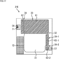
- FIG. 17 shows a sixth layout example of the pixel 21.
- the PD 31 is disposed on the lower side, and the memory unit 33 is disposed on the upper side.
- a high-concentration N-type region 56 is disposed on the left side in FIG. 17 via the second transfer transistor 34 with respect to the memory unit 33, and a pixel transistor region 72 on the left side in FIG. Be placed.
- discharge transistors 39-1 and 39-2 provided in series in the vertical direction are arranged on the right side in FIG. That is, the pixel 21 of FIG. 4 has a different configuration in that the drain transistors 39-1 and 39-2 are arranged in series in the left-right direction.
- the discharge transistors 39-1 and 39-2 may be arranged in any direction in the vertical direction or the horizontal direction, and may be arranged in series between the PD 31 and the high-concentration N-type region 57. That's fine.
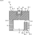
- FIG. 18 shows a seventh layout example of the pixel 21.
- the PD 31 is arranged on the lower side and the memory unit 33 is arranged on the upper side, like the pixel 21 in FIG. Further, a high-concentration N-type region 56 is disposed on the left side in FIG. 18 via the second transfer transistor 34 with respect to the memory unit 33, and a pixel transistor region 72 on the left side in FIG. Be placed.
- discharge transistors 39-1 and 39-2 provided in series in the vertical direction are arranged on the right side in FIG. 18 with respect to the PD 31, like the pixel 21E in FIG. Further, in the pixel 21F, the discharge transistor 39-2 is formed so as to surround the PD31 side and the discharge transistor 39-1 side of the high concentration N-type region 57.
- the discharge transistors 39-1 and 39-2 may be arranged in any direction in the vertical direction or the horizontal direction, and may be arranged in series between the PD 31 and the high-concentration N-type region 57. That's fine. Further, the shape of the discharge transistor 39-2 is not limited to a rectangle.
- FIG. 19 shows an eighth layout example of the pixel 21.
- the PD 31 is arranged on the lower side and the memory unit 33 is arranged on the upper side, like the pixel 21 in FIG.
- the pixel 21G has a high-concentration N-type region 56 disposed on the left side in FIG. 19 with respect to the memory unit 33 via the second transfer transistor 34, and the pixel 21G has a pixel on the left side in FIG.
- Transistor region 72 is disposed.
- discharge transistors 39-1 and 39-2 having a non-linear shape are arranged on the right side in FIG. That is, the pixel 21G has a layout in which the shape of the discharge transistors 39-1 and 39-2 is different from that of the pixel 21 in FIG.
- the shape of the discharge transistors 39-1 and 39-2 arranged between the PD 31 and the high concentration N-type region 57 is bent so as to surround the three sides on the PD 31 side of the high concentration N-type region 57. It can be a shape. That is, in the pixel 21G, if the discharge transistors 39-1 and 39-2 can be arranged in series between the PD 31 and the high-concentration N-type region 57, the discharge transistors 39 having various shapes other than the linear shape can be used. -1 and 39-2 can be employed.
- FIG. 20 shows a ninth layout example of the pixel 21.
- the PD 31 is disposed on the lower side, and the memory unit 33 is disposed on the upper side. Further, a high-concentration N-type region 56 is disposed on the left side in FIG. 20 via the second transfer transistor 34 with respect to the memory unit 33, and a pixel transistor region 72 is disposed on the left side in FIG. Be placed.
- the high-concentration N-type region 57 is disposed on the right side in FIG. 20 with respect to the PD 31 via the discharge transistors 39-1 to 39-3. That is, the pixel 21H has a layout different from that of the pixel 21 in FIG. 4 in that it includes three discharge transistors 39-1 to 39-3.
- the three discharges are not limited to the configuration in which the two discharge transistors 39-1 and 39-2 are arranged between the PD 31 and the high-concentration N-type region 57 as in the pixel 21 of FIG.
- a configuration in which the transistors 39-1 to 39-3 are arranged can be employed.
- a configuration in which three or more discharge transistors 39 are arranged in series may be adopted.
- FIG. 21 shows a tenth layout example of the pixel 21.
- the PD 31 is arranged on the lower side and the memory unit 33 is arranged on the upper side, like the pixel 21 in FIG.
- a high-concentration N-type region 56 is disposed on the left side in FIG. 21 via the second transfer transistor 34 with respect to the memory unit 33, and a pixel transistor region 72 on the left side in FIG. Be placed.
- discharge transistors 39-1 and 39-2 which are not in a linear shape are arranged on the right side in FIG. That is, the pixel 21J has a layout in which the shape of the discharge transistors 39-1 and 39-2 is different from that of the pixel 21 in FIG.
- the shape of the discharge transistor 39-2 arranged between the PD 31 and the high concentration N-type region 57 is such that the center protrudes toward the PD 31 side so as to surround the high concentration N-type region 57.
- the shape may be a substantially triangular shape.
- the discharge transistor 39-1 can have a bent shape along two sides of the PD 31 of the discharge transistor 39-2. That is, in the pixel 21J, if the discharge transistors 39-1 and 39-2 can be arranged in series between the PD 31 and the high-concentration N-type region 57, the discharge transistors 39 having various shapes other than the linear shape can be used. -1 and 39-2 can be employed.
- the voltage for driving the discharge transistors 39-1 and 39-2 is not limited to the binary value of the Hi level or the Low level, and an arbitrary level voltage can be set.
- the image pickup device 11 of each embodiment as described above includes various types such as an image pickup system such as a digital still camera or a digital video camera, a mobile phone having an image pickup function, or another device having an image pickup function. It can be applied to other electronic devices.
- an image pickup system such as a digital still camera or a digital video camera
- a mobile phone having an image pickup function or another device having an image pickup function. It can be applied to other electronic devices.
- FIG. 22 is a block diagram illustrating a configuration example of an imaging device mounted on an electronic device.
- the imaging apparatus 101 includes an optical system 102, an imaging element 103, a signal processing circuit 104, a monitor 105, and a memory 106, and can capture still images and moving images.
- the optical system 102 includes one or more lenses, guides image light (incident light) from a subject to the image sensor 103, and forms an image on a light receiving surface (sensor unit) of the image sensor 103.
- the image sensor 11 of the above-described embodiment is applied.
- the image sensor 103 electrons are accumulated for a certain period according to an image formed on the light receiving surface via the optical system 102. Then, a signal corresponding to the electrons accumulated in the image sensor 103 is supplied to the signal processing circuit 104.
- the signal processing circuit 104 performs various signal processing on the pixel signal output from the image sensor 103.
- An image (image data) obtained by performing signal processing by the signal processing circuit 104 is supplied to the monitor 105 and displayed, or supplied to the memory 106 and stored (recorded).
- the imaging apparatus 101 configured in this manner, by applying the imaging element 11 of the above-described embodiment, for example, an adverse effect caused by changing the potential of the overflow drain OFD can be avoided, and a higher quality image can be obtained. An image can be taken.
- FIG. 23 is a diagram illustrating a usage example in which the above-described imaging element 11 (image sensor) is used.
- the image sensor described above can be used in various cases for sensing light such as visible light, infrared light, ultraviolet light, and X-ray as follows.
- Devices for taking images for viewing such as digital cameras and mobile devices with camera functions
- Devices used for traffic such as in-vehicle sensors that capture the back, surroundings, and interiors of vehicles, surveillance cameras that monitor traveling vehicles and roads, and ranging sensors that measure distances between vehicles, etc.
- Equipment used for home appliances such as TVs, refrigerators, air conditioners, etc. to take pictures and operate the equipment according to the gestures ⁇ Endoscopes, equipment that performs blood vessel photography by receiving infrared light, etc.
- Equipment used for medical and health care ⁇ Security equipment such as security surveillance cameras and personal authentication cameras ⁇ Skin measuring instrument for photographing skin and scalp photography Such as a microscope to do beauty Equipment used for sports-Equipment used for sports such as action cameras and wearable cameras for sports applications-Used for agriculture such as cameras for monitoring the condition of fields and crops apparatus
- this technique can also take the following structures. (1) A photoelectric conversion unit that converts incident light into charges by photoelectric conversion and stores the charge; and A discharge unit for discharging the charge remaining in the photoelectric conversion unit; A plurality of pixels having a discharge drive unit that is driven when discharging charges from the photoelectric conversion unit to the discharge unit, A solid-state imaging device, wherein at least two or more discharge drive units are arranged in series between the photoelectric conversion unit and the discharge unit.
- the solid according to any one of (1) to (5) Image sensor. (7) A method for driving a solid-state imaging device,
- the solid-state imaging device is A photoelectric conversion unit that converts incident light into charges by photoelectric conversion and stores the charge; and A discharge unit for discharging the charge remaining in the photoelectric conversion unit;
- a photoelectric conversion unit that converts incident light into charges by photoelectric conversion and stores the charge; and A discharge unit for discharging the charge remaining in the photoelectric conversion unit; A plurality of pixels having a discharge drive unit that is driven when discharging charges from the photoelectric conversion unit to the discharge unit,
- An electronic apparatus comprising a solid-state imaging device, wherein at least two or more of the discharge drive units are arranged in series between the photoelectric conversion unit and the discharge unit.
Landscapes
- Engineering & Computer Science (AREA)
- Multimedia (AREA)
- Signal Processing (AREA)
- Solid State Image Pick-Up Elements (AREA)
- Transforming Light Signals Into Electric Signals (AREA)
Abstract
La présente invention se rapporte à un élément d'imagerie à semi-conducteurs, à un procédé de commande et à un dispositif électronique avec lesquels il est possible de capturer des images de qualité supérieure. Dans l'élément d'imagerie à semi-conducteurs, deux unités de commande de décharge ou plus sont montées en série entre une unité de conversion photoélectrique et une unité de décharge. Lorsqu'une image fixe est capturée et qu'une opération de réinitialisation pour l'unité de conversion photoélectrique est effectuée lorsque l'exposition des pixels commence, la commande est effectuée de sorte que le potentiel de toutes les unités de commande de décharge montées en série est réduit et la charge restante dans l'unité de conversion photoélectrique est déchargée vers l'unité de décharge, après cela, le potentiel de l'unité de commande de décharge du côté de l'unité de conversion photoélectrique est remis en premier au potentiel original, et ensuite les potentiels des autres unités de commande de décharge sont remis à leur potentiel original. La technologie de la présente invention peut être appliquée à un capteur d'image CMOS qui effectue, par exemple, une imagerie par un procédé d'obturation totale.
Priority Applications (2)
| Application Number | Priority Date | Filing Date | Title |
|---|---|---|---|
| US15/560,567 US10356348B2 (en) | 2015-04-03 | 2016-03-18 | Solid-state image capture element, driving method, and electronic device |
| US16/433,559 US10798324B2 (en) | 2015-04-03 | 2019-06-06 | Solid-state image capture element, driving method, and electronic device |
Applications Claiming Priority (2)
| Application Number | Priority Date | Filing Date | Title |
|---|---|---|---|
| JP2015-076686 | 2015-04-03 | ||
| JP2015076686 | 2015-04-03 |
Related Child Applications (2)
| Application Number | Title | Priority Date | Filing Date |
|---|---|---|---|
| US15/560,567 A-371-Of-International US10356348B2 (en) | 2015-04-03 | 2016-03-18 | Solid-state image capture element, driving method, and electronic device |
| US16/433,559 Continuation US10798324B2 (en) | 2015-04-03 | 2019-06-06 | Solid-state image capture element, driving method, and electronic device |
Publications (1)
| Publication Number | Publication Date |
|---|---|
| WO2016158483A1 true WO2016158483A1 (fr) | 2016-10-06 |
Family
ID=57005827
Family Applications (1)
| Application Number | Title | Priority Date | Filing Date |
|---|---|---|---|
| PCT/JP2016/058648 Ceased WO2016158483A1 (fr) | 2015-04-03 | 2016-03-18 | Élément d'imagerie à semi-conducteurs, procédé de commande et dispositif électronique |
Country Status (2)
| Country | Link |
|---|---|
| US (2) | US10356348B2 (fr) |
| WO (1) | WO2016158483A1 (fr) |
Cited By (7)
| Publication number | Priority date | Publication date | Assignee | Title |
|---|---|---|---|---|
| JP2018186267A (ja) * | 2017-04-26 | 2018-11-22 | パナソニックIpマネジメント株式会社 | 光検出装置 |
| US20190104268A1 (en) * | 2017-10-02 | 2019-04-04 | Sony Semiconductor Solutions Corporation | Solid-state imaging sensor and solid-state imaging device |
| JP2019106668A (ja) * | 2017-12-14 | 2019-06-27 | キヤノン株式会社 | 撮像装置 |
| JP2020068484A (ja) * | 2018-10-25 | 2020-04-30 | ソニー株式会社 | 固体撮像装置及び撮像装置 |
| WO2021002071A1 (fr) * | 2019-07-03 | 2021-01-07 | ソニーセミコンダクタソリューションズ株式会社 | Élément d'imagerie à semi-conducteurs, dispositif d'imagerie, et procédé de commande d'élément d'imagerie à semi-conducteurs |
| CN112997478A (zh) * | 2018-12-11 | 2021-06-18 | 索尼半导体解决方案公司 | 固态摄像装置和电子设备 |
| WO2025182307A1 (fr) * | 2024-02-26 | 2025-09-04 | ソニーセミコンダクタソリューションズ株式会社 | Dispositif d'imagerie à semi-conducteurs |
Families Citing this family (5)
| Publication number | Priority date | Publication date | Assignee | Title |
|---|---|---|---|---|
| KR102634245B1 (ko) | 2018-11-16 | 2024-02-07 | 삼성전자주식회사 | 이미지 센서 |
| CN111898433B (zh) * | 2020-06-22 | 2024-04-09 | 百望股份有限公司 | 一种纸质票据数字化方法和装置 |
| WO2022102404A1 (fr) * | 2020-11-12 | 2022-05-19 | ソニーセミコンダクタソリューションズ株式会社 | Élément d'imagerie à semi-conducteur, appareil électronique et procédé de commande d'élément d'imagerie à semi-conducteur |
| KR20220134324A (ko) | 2021-03-26 | 2022-10-05 | 삼성전자주식회사 | 이미지 센서 |
| KR20220144702A (ko) * | 2021-04-20 | 2022-10-27 | 삼성전자주식회사 | 픽셀 어레이 및 이를 포함하는 이미지 센서 |
Citations (3)
| Publication number | Priority date | Publication date | Assignee | Title |
|---|---|---|---|---|
| JP2011204878A (ja) * | 2010-03-25 | 2011-10-13 | Sony Corp | 固体撮像デバイスおよび電子機器 |
| JP2014060519A (ja) * | 2012-09-14 | 2014-04-03 | Sony Corp | 固体撮像素子及びその制御方法、並びに電子機器 |
| JP2016066766A (ja) * | 2014-09-26 | 2016-04-28 | ソニー株式会社 | 固体撮像装置、および電子装置 |
Family Cites Families (1)
| Publication number | Priority date | Publication date | Assignee | Title |
|---|---|---|---|---|
| US9461088B2 (en) * | 2014-12-01 | 2016-10-04 | Omnivision Technologies, Inc. | Image sensor pixel with multiple storage nodes |
-
2016
- 2016-03-18 US US15/560,567 patent/US10356348B2/en active Active
- 2016-03-18 WO PCT/JP2016/058648 patent/WO2016158483A1/fr not_active Ceased
-
2019
- 2019-06-06 US US16/433,559 patent/US10798324B2/en active Active
Patent Citations (3)
| Publication number | Priority date | Publication date | Assignee | Title |
|---|---|---|---|---|
| JP2011204878A (ja) * | 2010-03-25 | 2011-10-13 | Sony Corp | 固体撮像デバイスおよび電子機器 |
| JP2014060519A (ja) * | 2012-09-14 | 2014-04-03 | Sony Corp | 固体撮像素子及びその制御方法、並びに電子機器 |
| JP2016066766A (ja) * | 2014-09-26 | 2016-04-28 | ソニー株式会社 | 固体撮像装置、および電子装置 |
Cited By (16)
| Publication number | Priority date | Publication date | Assignee | Title |
|---|---|---|---|---|
| JP2018186267A (ja) * | 2017-04-26 | 2018-11-22 | パナソニックIpマネジメント株式会社 | 光検出装置 |
| JP7018583B2 (ja) | 2017-04-26 | 2022-02-14 | パナソニックIpマネジメント株式会社 | 光検出装置 |
| US20190104268A1 (en) * | 2017-10-02 | 2019-04-04 | Sony Semiconductor Solutions Corporation | Solid-state imaging sensor and solid-state imaging device |
| US10477133B2 (en) * | 2017-10-02 | 2019-11-12 | Sony Semiconductor Solutions Corporation | Solid-state imaging sensor and solid-state imaging device |
| JP2019106668A (ja) * | 2017-12-14 | 2019-06-27 | キヤノン株式会社 | 撮像装置 |
| JP7066392B2 (ja) | 2017-12-14 | 2022-05-13 | キヤノン株式会社 | 撮像装置 |
| JP7277106B2 (ja) | 2018-10-25 | 2023-05-18 | ソニーグループ株式会社 | 固体撮像装置及び撮像装置 |
| JP2020068484A (ja) * | 2018-10-25 | 2020-04-30 | ソニー株式会社 | 固体撮像装置及び撮像装置 |
| WO2020085265A1 (fr) * | 2018-10-25 | 2020-04-30 | Sony Corporation | Dispositif d'imagerie à semi-conducteur et dispositif d'imagerie |
| US12272711B2 (en) | 2018-10-25 | 2025-04-08 | Sony Group Corporation | Solid-state imaging device and imaging device |
| CN112868103A (zh) * | 2018-10-25 | 2021-05-28 | 索尼公司 | 固态摄像设备和摄像设备 |
| CN112997478A (zh) * | 2018-12-11 | 2021-06-18 | 索尼半导体解决方案公司 | 固态摄像装置和电子设备 |
| CN112997478B (zh) * | 2018-12-11 | 2024-03-19 | 索尼半导体解决方案公司 | 固态摄像装置和电子设备 |
| US11678079B2 (en) | 2019-07-03 | 2023-06-13 | Sony Semiconductor Solutions Corporation | Solid-state imaging element, imaging apparatus, and method of controlling solid-state imaging element |
| WO2021002071A1 (fr) * | 2019-07-03 | 2021-01-07 | ソニーセミコンダクタソリューションズ株式会社 | Élément d'imagerie à semi-conducteurs, dispositif d'imagerie, et procédé de commande d'élément d'imagerie à semi-conducteurs |
| WO2025182307A1 (fr) * | 2024-02-26 | 2025-09-04 | ソニーセミコンダクタソリューションズ株式会社 | Dispositif d'imagerie à semi-conducteurs |
Also Published As
| Publication number | Publication date |
|---|---|
| US10798324B2 (en) | 2020-10-06 |
| US20190289234A1 (en) | 2019-09-19 |
| US10356348B2 (en) | 2019-07-16 |
| US20180054579A1 (en) | 2018-02-22 |
Similar Documents
| Publication | Publication Date | Title |
|---|---|---|
| JP7496512B2 (ja) | 撮像装置 | |
| US10798324B2 (en) | Solid-state image capture element, driving method, and electronic device | |
| KR101799262B1 (ko) | 촬상소자 및 촬상장치 | |
| CN108174128B (zh) | 成像装置和电子设备 | |
| JP6873905B2 (ja) | 固体撮像装置および電子機器 | |
| KR101945052B1 (ko) | 고체 촬상 장치, 고체 촬상 장치의 구동 방법, 및 전자 기기 | |
| US20140312451A1 (en) | Solid-state imaging element, manufacturing method, and electronic device | |
| KR102553988B1 (ko) | 고체 촬상 소자 및 촬상 장치 | |
| WO2017169885A1 (fr) | Dispositif d'imagerie, procédé de commande, et dispositif électronique | |
| JP2017084892A (ja) | 撮像装置 | |
| CN107408566B (zh) | 固态成像设备和电子装置 | |
| JP2014165286A (ja) | フォトダイオード、固体撮像素子及び撮像装置 | |
| JP2015023250A (ja) | 固体撮像素子及びその駆動方法、並びに電子機器 | |
| JP2010114275A (ja) | 固体撮像装置、固体撮像装置の駆動方法、及び電子機器 | |
| US9338383B2 (en) | Method for driving solid-state imaging device including starting/ending a reset operation on pixels arranged in a two-dimensional array | |
| JP2014183064A (ja) | 固体撮像素子および製造方法、並びに電子機器 | |
| CN104282705B (zh) | 固态成像设备、其制造方法以及电子设备 | |
| JP5619093B2 (ja) | 固体撮像装置及び固体撮像システム |
Legal Events
| Date | Code | Title | Description |
|---|---|---|---|
| 121 | Ep: the epo has been informed by wipo that ep was designated in this application |
Ref document number: 16772366 Country of ref document: EP Kind code of ref document: A1 |
|
| WWE | Wipo information: entry into national phase |
Ref document number: 15560567 Country of ref document: US |
|
| NENP | Non-entry into the national phase |
Ref country code: DE |
|
| NENP | Non-entry into the national phase |
Ref country code: JP |
|
| 122 | Ep: pct application non-entry in european phase |
Ref document number: 16772366 Country of ref document: EP Kind code of ref document: A1 |