WO2016158517A1 - Électrodes et panneau tactile - Google Patents
Électrodes et panneau tactile Download PDFInfo
- Publication number
- WO2016158517A1 WO2016158517A1 PCT/JP2016/058799 JP2016058799W WO2016158517A1 WO 2016158517 A1 WO2016158517 A1 WO 2016158517A1 JP 2016058799 W JP2016058799 W JP 2016058799W WO 2016158517 A1 WO2016158517 A1 WO 2016158517A1
- Authority
- WO
- WIPO (PCT)
- Prior art keywords
- electrode
- group
- strip
- touch panel
- electrode pattern
- Prior art date
- Legal status (The legal status is an assumption and is not a legal conclusion. Google has not performed a legal analysis and makes no representation as to the accuracy of the status listed.)
- Ceased
Links
Images




Classifications
-
- G—PHYSICS
- G06—COMPUTING OR CALCULATING; COUNTING
- G06F—ELECTRIC DIGITAL DATA PROCESSING
- G06F3/00—Input arrangements for transferring data to be processed into a form capable of being handled by the computer; Output arrangements for transferring data from processing unit to output unit, e.g. interface arrangements
- G06F3/01—Input arrangements or combined input and output arrangements for interaction between user and computer
- G06F3/03—Arrangements for converting the position or the displacement of a member into a coded form
- G06F3/041—Digitisers, e.g. for touch screens or touch pads, characterised by the transducing means
Definitions
- the present invention relates to an electrode and a touch panel.
- a touch panel (Touch Panel) has been developed as an input device capable of inputting information such as text and graphics.
- the touch panel is provided on the display surface of displays such as electronic notebooks, liquid crystal display devices, flat panel display devices such as PDP (Plasma Display Panel), El (Electroluminescence), and CRT (Cathode Ray Tube). It is a device that is used to select information.
- displays such as electronic notebooks, liquid crystal display devices, flat panel display devices such as PDP (Plasma Display Panel), El (Electroluminescence), and CRT (Cathode Ray Tube). It is a device that is used to select information.
- Touch panel types are classified into resistive film type, capacitance type, electromagnetic type, surface acoustic wave type and infrared type. Such touch panels take into account signal amplification problems, resolution differences, difficulty of design and processing technology, optical characteristics, electrical characteristics, mechanical characteristics, environmental resistance characteristics, input characteristics, durability, economy, etc. And used in electronic products. Currently, the most widely used touch panels are a resistive touch panel and a capacitive touch panel.
- the touch panel a method for forming an electrode pattern using a metal has been developed.
- the electrode pattern is formed of metal, the electrode pattern has excellent electrical conductivity.
- the touch panel is required to have excellent visibility as well as excellent electrical conductivity.
- methods for improving the visibility of a touch panel methods described in Patent Documents 1 and 2 are known.
- Such a touch panel is formed so that electrodes for detecting a touch position have a predetermined pattern.
- a transparent electrode film made of a metal oxide such as ITO (IndiumdiTin Oxide) is widely used in order to make it possible to visually recognize an image of a liquid crystal display device formed in a lower layer.
- the transparent electrode film using a metal oxide has a problem of low conductivity.
- a touch panel is known in which a very thin and low-viscosity electrode is formed using a conductive ink in which a metal having excellent conductivity such as gold or silver is dispersed in a resin composition.
- the electrode formation pattern constituting the touch panel includes a grid pattern in which strip electrodes extending in different directions intersect, a waveform pattern in which a plurality of wavy strip electrodes combined with a plurality of bent portions are arranged in one direction at a predetermined interval, etc. Can be mentioned.
- an electrode pattern formed by regularly arranging strip-shaped electrodes has a problem that a part of the electrode is easily recognized at a specific position depending on the shape, and as a result, the visibility of the display image is hindered.
- a discontinuous island portion is formed between the wiring pattern portion formed in the waveform and the electrode pattern portion.
- two or more electrode patterns that are electrically separated from each other are arranged adjacent to each other.
- this portion since there is no electrode pattern between the electrode patterns adjacent to each other, this portion has higher light transmittance than the surrounding electrode pattern forming portion, resulting in non-uniform contrast of the display screen. There is a possibility that the visibility may be lowered.
- the arrangement pattern and the number of the grids of the first electrode and the second electrode adjacent to each other are determined in advance. Visibility is improved by forming according to the rules.
- a linear virtual pattern may be recognized by human illusion along the direction in which the vertices of the bent portions are arranged in the wiring pattern portion formed in a waveform. .
- the virtual pattern by such an illusion has a problem that the visibility of the touch panel is lowered.
- the configuration described in Patent Document 4 has a problem that visibility is not good because the repeated arrangement patterns of the grids of the first electrode and the second electrode are the same.
- the first electrode and the second electrode are separated from each other in order to suppress the occurrence of an electrical short circuit due to defective printing of the electrodes. It is necessary to let For this reason, the visibility of the separated part is lowered, and it has been difficult to achieve both improvement in visibility and elimination of a short circuit due to defective printing of the electrodes.
- the present invention has been made in view of the above circumstances, and an object thereof is to provide an electrode and a touch panel that can be easily formed and can improve the visibility of an electrode pattern.
- the electrode of the present invention includes a strip electrode extending in a predetermined direction, and has a dummy region formed in a part of the strip electrode or formed independently of the strip electrode.
- the band-shaped electrode includes a plurality of band-shaped electrodes forming a wavy line formed by combining a plurality of refracting portions along the first direction of the electrode forming surface with a predetermined interval along a second direction perpendicular to the first direction.
- a strip-shaped conductor that forms the dummy region is provided in the vicinity of the refracting portion and spaced apart from the strip-shaped electrode and extending in a dotted shape or a direction inclined with respect to the second direction.
- the band-shaped conductor extends along the first direction.
- the band-shaped conductors extend in random directions with respect to each other.
- the electrode forming surface has at least a first electrode pattern region and a second electrode pattern region provided with the belt-like electrode, and the first electrode pattern region and the second electrode pattern region are formed on the electrode forming surface. Adjacent and electrically separated through a predetermined separation region along a predetermined direction, the separation region extends at least with respect to the predetermined direction, is separated from the strip electrode, and A conductor forming a dummy region is arranged.
- a plurality of band-like electrodes extending along the first direction and the second direction of the electrode forming surface are crossed with each other to form a lattice-like unit electrode pattern, and a plurality of the unit electrode patterns are connected in series.
- An electrode having at least an electrode pattern region and a second electrode pattern region, wherein the first electrode pattern region and the second electrode pattern region are arranged adjacent to each other in an adjacent portion and electrically separated, and the adjacent portion In the direction in which the end of the strip electrode in the first electrode pattern region and the end of the strip electrode in the second electrode pattern region intersect the first direction and the second direction of the electrode formation surface It has the overlapping part which forms the said dummy area
- the overlapped portion is characterized in that at least one of thickness and width is reduced as compared with other portions.
- the overlapped portion is formed in a dotted line shape.
- the touch panel of the present invention is characterized by comprising a transparent base material and the electrode described in each of the above items formed on the transparent base material.
- an electrode and a touch panel that can be easily formed and can improve the visibility of the electrode pattern.
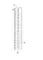
- FIG. 2 is a cross-sectional view taken along line AA in FIG. It is the principal part enlarged plan view which expanded D area
- FIG. 1 is a cross-sectional view taken along line AA in FIG. It is the principal part enlarged plan view which expanded D area
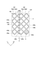
- FIG. 9 is a cross-sectional view taken along the line A-A ′ of FIG. 8. It is the principal part expansion perspective view which expanded D area
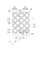
- FIG. 14 is a cross-sectional view taken along line A-A ′ of FIG. 13. It is the principal part enlarged plan view which expanded D area
- Embodiments of the electrode and touch panel of the present invention will be described. Note that this embodiment is specifically described in order to better understand the gist of the invention, and does not limit the present invention unless otherwise specified.
- the drawings used in the following description in order to make the features of the present invention easier to understand, there is a case where a main part is shown in an enlarged manner for convenience, and the dimensional ratio of each component is the same as the actual one. Not necessarily.
- an electrode for a touch panel and a touch panel including the electrode will be described as an example.
- FIG. 1 is a schematic plan view showing a touch panel provided with electrodes for a touch panel in the first embodiment.
- FIG. 2 is a cross-sectional view taken along line AA ′ of FIG.
- FIG. 3 is an enlarged plan view of a region surrounded by a dotted line D in FIG.
- the touch panel 10 of this embodiment includes a transparent base material (substrate) 20 and a touch panel electrode (electrode) 50 formed on an electrode forming surface 20a that is one surface of the transparent base material 20.
- the touch panel electrode 50 includes a plurality of strip-shaped electrodes 30 and a conductor (dummy region) 40 provided separately from the strip-shaped electrodes 30.
- a liquid crystal display panel (not shown) or the like is disposed under the transparent base (substrate) 20 (lower layer).
- the strip electrode 30 is formed so as to form a non-linear wavy line in which a plurality of refracting portions 31 are combined along the first direction (referred to as the Y direction in this embodiment) of the electrode forming surface 20a.
- a plurality of strip electrodes 30 formed in such wavy lines are arranged at a predetermined interval (predetermined pitch) along the second direction (referred to as the X direction in this embodiment) of the electrode forming surface 20a.
- predetermined pitch predetermined pitch
- the refracting portion 31 of the strip electrode 30 is a region refracted at an angle where the inner angle ⁇ is greater than 90 °, for example.
- the internal angle ⁇ of the refracting portion 31 may be about 120 ° to 150 °, for example, but is not particularly limited.
- the plurality of strip electrodes 30 are arranged so that the apex P of the refracting portion 31 is positioned on a line along the X direction.
- a large number of conductors (dummy regions) 40 are arranged apart from the strip electrode 30.
- Each conductor 40 is made of a conductive material formed in a strip shape.
- a large number of conductors 40 are arranged adjacent to the apex P of the refracting portion 31 of the strip electrode 30 so that the long sides extend in a direction inclined with respect to the X direction. That is, in the present embodiment, a large number of conductors 40 are arranged so that the long side is along the Y direction inclined 90 ° with respect to the X direction.
- the visual recognition of the virtual line Oi due to the illusion that occurs when observing the arrangement of the band-like band-like electrodes 30 is prevented. That is, when the band-shaped electrode 30 of the wavy line is arranged along the X direction, a virtual line Oi connecting the vertices P of the refracting portions 31 of the adjacent band-shaped electrodes 30 may be seen by an illusion. There is a possibility that the visibility of 10 may be lowered.
- the strip-shaped conductor 40 extending in the direction in which the long side is inclined with respect to the Y direction that is the extending direction of the virtual line Oi is disposed in the vicinity of the refracting portion 31 of the strip electrode 30.
- the virtual line Oi can be prevented from being visually recognized by an illusion.
- an image displayed on the touch panel 10 can be seen more clearly, and the visibility of the touch panel 10 can be improved.
- a plurality of conductors 40 are arranged apart from the strip electrode 30 to arrange the wavy strip electrodes 30.
- the conductor 40 is formed at all corresponding positions (near) of the refracting part 31, but the conductor 40 is formed only near a part of the refracting part 31. You can also.
- the conductor (dummy region) 40 is formed only in the vicinity of the refracting portion 31 of the band-shaped electrode 30 selected at random.
- the degree of formation of the conductor 40 can be, for example, the number thinned to such an extent that the virtual line Oi is prevented from being visually recognized.
- FIG. 4 is an enlarged plan view of a main part showing a touch panel provided with electrodes for the touch panel according to the second embodiment of the present invention.
- the touch panel 60 of the present embodiment includes a transparent substrate 20 and a touch panel electrode (electrode) 70 formed on the electrode forming surface (one surface) 20 a of the transparent substrate 20.
- the touch panel electrode 70 is composed of a plurality of strip electrodes 30 and a conductor (dummy region) 80 provided apart from the strip electrodes 30.
- the strip electrode 30 is formed so as to form a non-linear wavy line in which a plurality of refracting portions 31 are combined along the first direction (referred to as the Y direction in this embodiment) of the electrode forming surface 20a.
- a plurality of strip electrodes 30 formed in such wavy lines are arranged at a predetermined interval (predetermined pitch) along the second direction (referred to as the X direction in this embodiment) of the electrode forming surface 20a.
- predetermined pitch predetermined pitch
- a large number of conductors (dummy regions) 80 are arranged apart from the strip electrode 30.
- the conductor 80 of the present embodiment constitutes one (one) conductor 80 in which point-like conductive materials are arranged, for example, along the Y direction.
- a large number of conductors 80 in which such dotted conductive materials are arranged are arranged adjacent to the apex P of the refracting portion 31 of the strip electrode 30.
- the conductor 80 can be formed at a position corresponding to an arbitrary refracting portion 31 without forming the conductor 80 at a position corresponding to all the refracting portions 31.
- FIG. 5 is an enlarged plan view of a main part showing a touch panel provided with electrodes for the touch panel according to the third embodiment of the present invention.
- the touch panel 90 of the present embodiment includes a transparent substrate 20 and a touch panel electrode (electrode) 100 formed on an electrode formation surface (one surface) 20 a of the transparent substrate 20.
- the touch panel electrode 100 is composed of a plurality of strip electrodes 30 and a conductor (dummy region) 110 provided separately from the strip electrodes 30.
- the strip electrode 30 is formed so as to form a non-linear wavy line in which a plurality of refracting portions 31 are combined along the first direction (referred to as the Y direction in this embodiment) of the electrode forming surface 20a.
- the touch panel electrode 90 is formed by arranging a plurality of strip-shaped electrodes 30 formed in such wavy lines at predetermined intervals (predetermined pitch) along a second direction (referred to as X direction in the present embodiment) of the electrode forming surface 20a. Has been.
- a large number of conductors (dummy regions) 110 are arranged apart from the strip electrode 30.
- a large number of strip-shaped conductive materials are arranged adjacent to the apex P of the refracting portion 31 of the strip-shaped electrode 30.
- the individual conductors 110 are formed, for example, such that the long sides thereof are along one direction S1 and the other direction S2 constituting the refracting portion 31 of the strip electrode 30.
- the conductor 110 can be formed at a position corresponding to an arbitrary refracting portion 31 without forming the conductor 110 at a position corresponding to all the refracting portions 31.
- FIG. 6 is a main part enlarged plan view showing a touch panel provided with electrodes for a touch panel according to a fourth embodiment of the present invention.
- the touch panel 120 of this embodiment includes a transparent substrate 20 and a touch panel electrode (electrode) 130 formed on an electrode formation surface (one surface) 20 a of the transparent substrate 20.
- the touch panel electrode 130 is composed of a plurality of strip electrodes 30 and a conductor (dummy region) 140 provided separately from the strip electrodes 30.
- the strip electrode 30 is formed so as to form a non-linear wavy line in which a plurality of refracting portions 31 are combined along the first direction (referred to as the Y direction in this embodiment) of the electrode forming surface 20a.
- a plurality of strip-like electrodes 30 formed in such wavy lines are arranged at a predetermined interval (predetermined pitch) along the second direction (referred to as the X direction in this embodiment) of the electrode forming surface 20 a.
- predetermined pitch predetermined pitch
- a large number of conductors (dummy regions) 140 are arranged apart from the strip electrode 30.
- a large number of strip-shaped conductive materials are arranged adjacent to the apex P of the refracting portion 31 of the strip-shaped electrode 30.
- the individual conductors 140 are arranged so that the direction of the long side is inclined with respect to the X direction and the formation positions are random.
- the individual conductors 140 are arranged so that the formation positions are random.
- the individual conductors 140 may be formed so that the orientation (angle with respect to the X direction) of the individual conductors is random. it can. In this case, the formation position of the conductor 140, at least one of the directions of the conductor 140, or both can be made random.
- the size and shape of the conductor are not particularly limited, and can be any size and any shape.
- the conductor may be a dot shape, a triangle shape, a quadrangular shape, a pentagonal or more polygonal shape, a star shape, or the like.
- each conductor is not particularly limited as long as it is in the vicinity of the bent portion of the wavy band-shaped electrode, and at an arbitrary angle with respect to the second direction at an arbitrary position in the vicinity of the bent portion. It can be formed to extend in the inclined direction.
- an insulating layer is further formed so as to cover the strip electrode and the conductor formed on the electrode forming surface of the transparent substrate.
- FIG. 8 is a schematic plan view showing a touch panel provided with electrodes for a touch panel in the fifth embodiment.
- FIG. 9 is a cross-sectional view taken along the line AA ′ of FIG.
- FIG. 10 is an enlarged plan view of a region surrounded by a dotted line D in FIG.
- the touch panel 210 of the present embodiment includes a transparent base material (substrate) 220 and a touch panel electrode (electrode) 250 formed on an electrode forming surface 220a which is one surface of the transparent base material 220.
- the touch panel electrode 250 includes a pattern electrode formed by crossing a plurality of strip electrodes 230 and a conductor 240.
- a liquid crystal display panel (not shown) or the like is disposed under the transparent base material (substrate) 220 (lower layer).
- the strip electrode 230 is for a grid-shaped touch panel in which a plurality of strip electrodes 230a extending along the X direction in the drawing and a plurality of strip electrodes 230b extending along the Y direction in the drawing intersect at a predetermined angle.
- An electrode 250 is formed. That is, a grid-shaped touch panel electrode 250 is formed by providing a number of rectangular unit electrode patterns S connected in series.
- the crossing angle between the plurality of strip electrodes 230a extending along the X direction and the plurality of strip electrodes 230b extending along the Y direction is, for example, 90 °. That is, the strip electrode 230a and the strip electrode 230b are orthogonal to each other to constitute a touch panel electrode 250 having a mesh structure (mesh structure).
- the touch panel electrode 250 includes a first electrode pattern region E1 and a second electrode pattern region E2 arranged along a predetermined direction of the electrode formation surface 220a on the electrode formation surface 220a, and the first electrode pattern region E1 and the first electrode pattern region E1.
- a two-electrode pattern region E2 has a separation region E3 that is a separation region.
- the predetermined direction in which the first electrode pattern region E1 and the second electrode pattern region E2 are separated from each other is the X direction in the drawing.
- the separation region E3 is a region where the first electrode pattern region E1 and the second electrode pattern region E2 spread over a portion separated by a predetermined distance.
- the first electrode pattern region E1 and the second electrode pattern region E2 that are formed apart from each other are electrically separated from each other. That is, the strip electrode 230 in the first electrode pattern region E1 and the strip electrode 230 in the second electrode pattern region E2 are not connected to each other.
- the first electrode pattern region E1 and the second electrode pattern region E2 may be an electrode pattern to which a voltage is actually applied or a dummy electrode pattern.
- a large number of conductors (dummy regions) 240 are arranged in a separation region E3 provided between the first electrode pattern region E1 and the second electrode pattern region E2.
- Such a conductor 240 has a region extending at least in a predetermined direction of the electrode formation surface 220a, in this embodiment, an angle direction inclined with respect to the X direction, and is separated from the strip electrode 230. It is.
- the conductor 240 is formed in a rectangular parallelepiped shape extending in a direction inclined at an angle ⁇ with respect to the X direction, and the angle ⁇ is set to 45 °, for example.
- the first electrode pattern region E1 and the second electrode pattern region E2 extend in a direction inclined at an angle ⁇ with respect to the X direction to the separation region E3 that electrically separates the first electrode pattern region E1 and the second electrode pattern region E2.
- the conductor 240 it is possible to prevent the visibility of the separation region E3 where no electrode pattern exists from being lower than that of the peripheral portion. Thereby, an image displayed on the touch panel 210 can be seen more clearly, and the visibility of the touch panel 210 can be improved.
- the conductor 240 that improves the visibility of the separation region E3 is provided in a predetermined direction of the electrode forming surface 220a, that is, in the present embodiment, the first.
- the conductor 240 In order to avoid a short circuit when forming the first electrode pattern region E1 and the second electrode pattern region E2 by inclining with respect to the X direction which is the separation direction of the electrode pattern region E1 and the second electrode pattern region E2. Space can be secured. Thereby, even if the conductor 240 is formed in the separation region E3, it is possible to reliably prevent a short circuit between the first electrode pattern region E1 and the second electrode pattern region E2.
- FIG. 11 is a principal part enlarged plan view which shows the touchscreen provided with the electrode for touchscreens of 6th embodiment of this invention.
- the touch panel 260 of the present embodiment includes a transparent base material (substrate) 220 and a touch panel electrode (electrode) 70 formed on an electrode forming surface 220 a that is one surface of the transparent base material 220.
- the touch panel electrode 270 includes a pattern electrode formed by crossing a plurality of strip electrodes 280 and a conductor (dummy region) 290.
- the strip electrode 280 is a grid-shaped touch panel in which a plurality of strip electrodes 280a extending along the X direction in the drawing and a plurality of strip electrodes 280b extending along the Y direction intersect at a predetermined angle, for example, 90 °.
- the electrode 270 is formed.
- the electrode 270 for the touch panel is a first electrode pattern region E1 that is two electrode pattern regions spaced apart in a predetermined direction, for example, the X direction in the drawing, via the predetermined separation region E3 on the electrode formation surface 220a. And a second electrode pattern region E2.
- a large number of conductors 290 are arranged in a separation region E3 provided between the first electrode pattern region E1 and the second electrode pattern region E2.
- the conductor 290 of the present embodiment is a strip-shaped conductor that includes at least a region extending in an angle direction inclined with respect to the X direction, which is a predetermined direction of the electrode formation surface 220a, and is separated from the strip electrode 280. is there.
- the conductor 290 has a hook-like shape composed of a region extending along the Y direction, which is a direction inclined at an angle of 90 ° with respect to the X direction, and regions extending in the X direction from both ends of this region. It consists of the formed conductor.
- the separation region E3 that electrically separates the first electrode pattern region E1 and the second electrode pattern region E2 from each other includes a region extending in a direction inclined with respect to the X direction.
- the hook-shaped conductor (dummy region) 290 it is possible to prevent the visibility of the separation region E3 where no electrode pattern exists from being lower than the peripheral portion. Thereby, an image displayed on the touch panel 260 can be seen more clearly, and the visibility of the touch panel 260 can be improved.
- FIG. 12 is an enlarged plan view of a main part showing a touch panel provided with electrodes for the touch panel according to the seventh embodiment of the present invention.
- the touch panel 300 of this embodiment includes a transparent base material (substrate) 320 and a touch panel electrode (electrode) 310 formed on an electrode forming surface 320a which is one surface of the transparent base material 320.
- the touch panel electrode 310 includes a pattern electrode formed by intersecting a plurality of strip electrodes 320 and a conductor (dummy region) 330.
- the strip electrode 320 includes a grid-shaped touch panel in which a plurality of strip electrodes 320a extending along the X direction in the drawing and a plurality of strip electrodes 320b extending along the Y direction intersect at a predetermined angle, for example, 90 °.
- a working electrode 310 is formed.
- the touch panel electrode 310 is a first electrode pattern region E1 which is two electrode pattern regions spaced apart in a predetermined direction, for example, the X direction in the figure, via a predetermined separation region E3 on the electrode formation surface 320a. And a second electrode pattern region E2.
- a large number of conductors (dummy regions) 330 are arranged in a separation region E3 provided between the first electrode pattern region E1 and the second electrode pattern region E2.
- the conductor 330 of the present embodiment is a point-like conductor arranged in an angle direction inclined with respect to the X direction which is a predetermined direction of the electrode forming surface 320a.
- one conductor 330 is composed of a set of three point-like conductors (dot-like conductor group).
- the touch panel 300 having such a configuration, the arrangement direction of a set of three point-like conductors in the separation region E3 that electrically separates the first electrode pattern region E1 and the second electrode pattern region E2 from each other.
- the conductors (dummy regions) 330 arranged in a direction inclined with respect to the X direction, it is possible to prevent the visibility of the separation region E3 where no electrode pattern exists from being lower than the peripheral portion thereof. . Thereby, an image displayed on the touch panel 300 can be seen more clearly, and the visibility of the touch panel 300 can be improved.
- the conductor may be composed of a mixture of strips and dots. Moreover, as long as the conductor includes at least a region extending in a direction inclined at an arbitrary angle with respect to a predetermined direction of the electrode formation surface, the other portions may be parallel to the predetermined direction.
- random means that a plurality of conductors are formed in random directions as long as the extending direction of the conductors is inclined with respect to a predetermined direction, or the formation positions in the separation region E3. Are formed at random positions without regularization.
- the conductor exists in the separation region E3, and the other part may be applied to the first electrode pattern region E1 and the second electrode pattern region E2.
- the shapes of the individual conductors do not have to be the same as each other, and conductors having different shapes can be randomly arranged.
- each unit electrode pattern has a diamond shape.
- an insulating layer is further formed so as to cover the strip electrode and the conductor formed on the electrode forming surface of the transparent substrate.
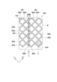
- FIG. 13 is a schematic plan view which shows the touchscreen provided with the electrode for touchscreens in 8th embodiment.
- FIG. 14 is a cross-sectional view taken along the line AA ′ of FIG.
- FIG. 15 is an enlarged plan view of a region surrounded by a dotted line D in FIG.
- the touch panel 410 of the present embodiment includes a transparent base material (substrate) 420 and a touch panel electrode (electrode) 450 formed on an electrode forming surface 420 a that is one surface of the transparent base material 420.
- the touch panel electrode 450 includes a pattern electrode formed by crossing a plurality of strip electrodes 430 with each other.
- a liquid crystal display panel (not shown) or the like is disposed under the transparent base material (substrate) 420 (lower layer).
- the strip electrode 430 includes a plurality of strip electrodes 430a extending along the first direction (referred to as L1 direction in the present embodiment) and a plurality of strip electrodes extending along the second direction (referred to as L2 direction in the present embodiment).
- 430b intersects at an angle ⁇ to form a grid-like touch panel electrode 450. That is, a grid-shaped touch panel electrode 450 is formed by providing a number of rectangular unit electrode patterns S connected in series.
- the angle ⁇ is, for example, 90 °
- the strip electrode 430a and the strip electrode 430b are orthogonal to each other to form a touch panel electrode 450 having a mesh structure (mesh structure). .
- the touch panel electrode 450 includes a first electrode pattern region E1 and a second electrode pattern region E2, which are two electrode pattern regions disposed adjacent to each other on the electrode formation surface 420a.
- the first electrode pattern region E1 and the second electrode pattern region E2 are electrically separated from each other. That is, the strip electrode 430 in the first electrode pattern region E1 and the strip electrode 430 in the second electrode pattern region E2 are not connected to each other.
- the first electrode pattern region E1 and the second electrode pattern region E2 may be an electrode pattern to which a voltage is actually applied or a dummy electrode pattern.
- an end portion 430e of the strip electrode 430 constituting the first electrode pattern region E1 and the second electrode pattern region E2 are formed on the side where the first electrode pattern region E1 and the second electrode pattern region E2 face each other (adjacent).
- the end portion 430e of the strip electrode 430 forms an overlapping portion (dummy region) 430W that overlaps with each other in the direction intersecting the first direction L1 and the second direction L2.
- the first electrode pattern region E1 and the second electrode pattern are indicated by an arrow V that intersects the first direction L1 and the second direction L2 and indicates the direction along the electrode formation surface 420a.
- the end portions 430e of the respective strip electrodes 430 form an overlapping portion 430W that overlaps each other.
- overlapping portions (dummy regions) 430W form a region including the end portion 430e of the strip electrode 430 formed integrally with the strip electrode 430. That is, the overlapping portion 430W is obtained by shifting the phases of the first electrode pattern region E1 and the second electrode pattern region E2 formed at the same pitch and approaching each other.
- the formation pitch of the strip electrodes 430 in the first electrode pattern region E1 and the second electrode pattern region E2 is the same, but the strip electrodes 430 in the first electrode pattern region E1 and the second electrode pattern region E2 are the same.
- the overlapping portion 430W can also be formed by changing the formation pitch of each other.
- the end portions 430e of the strip electrodes 430 are overlapped with the adjacent portions of the first electrode pattern region E1 and the second electrode pattern region E2 that are electrically separated from each other.
- the overlapping portion (dummy region) 430W By forming the overlapping portion (dummy region) 430W, the visibility of the adjacent portions between the electrode patterns can be prevented from being lower than that of the peripheral portions. Thereby, an image displayed on the touch panel 410 can be seen more clearly, and the visibility of the touch panel 410 can be improved.
- FIG. 16 is a principal part enlarged plan view which shows the touchscreen provided with the electrode for touchscreens of 9th embodiment of this invention.
- the touch panel 460 of the present embodiment includes a transparent base material (substrate) 420 and a touch panel electrode (electrode) 470 formed on an electrode forming surface 420 a that is one surface of the transparent base material 420.
- the touch panel electrode 470 includes a pattern electrode formed by crossing a plurality of strip electrodes 480.
- the strip-shaped electrode 480 includes a plurality of strip-shaped electrodes 480a extending along the first direction L1 and a plurality of strip-shaped electrodes 480b extending along the second direction L2 intersecting at an angle ⁇ , so that the grid-shaped touch panel electrode 470 is formed.
- a grid-shaped touch panel electrode 470 is formed by providing a number of rectangular unit electrode patterns S connected in series.
- the angle ⁇ is, for example, 90 °
- the strip electrode 480a and the strip electrode 480b are orthogonal to each other to constitute a touch panel electrode 470 having a mesh structure (mesh structure). .
- the touch panel electrode 470 includes a first electrode pattern region E1 and a second electrode pattern region E2, which are two electrode pattern regions disposed adjacent to each other on the electrode formation surface 420a.
- the first electrode pattern region E1 and the second electrode pattern region E2 are electrically separated from each other.
- an end portion 80e of the strip electrode 480 constituting the first electrode pattern region E1 and the second electrode pattern region E2 are formed on the side where the first electrode pattern region E1 and the second electrode pattern region E2 face each other (adjacent).
- the end portion 480e of the strip electrode 480 forms an overlapping portion (dummy region) 480W that overlaps with each other in the direction intersecting the first direction L1 and the second direction L2.
- the end portion 480e of the strip electrode 480 is formed in a dotted line shape in which dotted conductors are arranged along the first direction L1 and the second direction L2.
- the formation interval and size of the dotted conductors can be arbitrarily selected.
- the end portion 480e of the strip-shaped electrode 480 formed in a dotted line is formed in the adjacent portion between the first electrode pattern region E1 and the second electrode pattern region E2 that are electrically separated from each other.
- the overlapped portion (dummy region) 480W that is overlapped, the visibility of the adjacent portion between the electrode patterns can be prevented from being lower than that of the peripheral portion. Thereby, an image displayed on the touch panel 460 can be seen more clearly, and the visibility of the touch panel 460 can be improved.
- FIG. 17 is a principal part enlarged plan view which shows the touchscreen provided with the electrode for touchscreens of 10th Embodiment of this invention.
- the touch panel 590 of the present embodiment includes a transparent base material (substrate) 520 and a touch panel electrode (electrode) 500 formed on an electrode forming surface 520a which is one surface of the transparent base material 520.
- the touch panel electrode 500 is composed of a pattern electrode formed by crossing a plurality of strip electrodes 510 with each other.
- the strip-shaped electrode 510 includes a plurality of strip-shaped electrodes 510a extending along the first direction L1 and a plurality of strip-shaped electrodes 510b extending along the second direction L2 intersecting at an angle ⁇ to form a grid-shaped touch panel electrode 500.
- a grid-shaped touch panel electrode 500 is formed by providing a number of rectangular unit electrode patterns S connected in series.
- the angle ⁇ is, for example, 90 °
- the band-shaped electrode 510a and the band-shaped electrode 510b are orthogonal to each other to form a touch panel electrode 500 having a mesh structure (mesh structure). .
- the touch panel electrode 500 includes a first electrode pattern region E1 and a second electrode pattern region E2, which are two electrode pattern regions disposed adjacent to each other on the electrode formation surface 20a.
- the strip electrode 510 in the first electrode pattern region E1 and the strip electrode 510 in the second electrode pattern region E2 are electrically separated from each other.
- an end portion 510e of the strip-like electrode 510 constituting the first electrode pattern region E1 and the second electrode pattern region E2 are formed.
- An end portion 510e of the strip electrode 510 forms an overlapping portion (dummy region) 510W that overlaps with each other in the direction intersecting the first direction L1 and the second direction L2.
- the width of the end portion 510e of the strip electrode 510 constituting the overlapping portion (dummy region) 510W is smaller than that of the other portions. That is, the width G1 of the end portion 510e of the belt-like electrode 510 is formed to be half the size (half-width) of the width G2 in the region other than the overlapping portion (dummy region) 510W of the belt-like electrode 510. Note that the width G1 of the end portion 510e of the belt-like electrode 510 only needs to be smaller than the width G2 in a region other than the overlapping portion (dummy region) 510W of the belt-like electrode 510, and is not limited to a half width.
- the touch panel 590 having such a configuration, adjacent portions of the first electrode pattern region E1 and the second electrode pattern region E2 that are electrically separated from each other other than the overlapping portion (dummy region) 510W of the belt-like electrode 510 are provided.
- an overlapping portion (dummy region) 510W in which the end portions 510e of the strip-like electrode 510 formed to have a width G1 smaller than the width G2 in the region are overlapped, the visibility of the adjacent portions between the electrode patterns is improved in the peripheral portion. Can be prevented. Thereby, an image displayed on the touch panel 90 can be seen more clearly, and the visibility of the touch panel 90 can be improved.
- FIG. 18 is a main part enlarged plan view showing a touch panel including electrodes for a touch panel according to the eleventh embodiment of the present invention.
- the touch panel 520 of the present embodiment includes a transparent base material (substrate) 520 and a touch panel electrode (electrode) 530 formed on an electrode forming surface 520 a that is one surface of the transparent base material 520.
- the touch panel electrode 530 is composed of a pattern electrode formed by crossing a plurality of strip electrodes 540 with each other.
- the strip-shaped electrode 540 includes a plurality of strip-shaped electrodes 540a extending along the first direction L1 and a plurality of strip-shaped electrodes 540b extending along the second direction L2 intersecting at an angle ⁇ , so that the grid-shaped touch panel electrode 530 is formed.
- a grid-shaped touch panel electrode 530 is formed by providing a large number of rectangular unit electrode patterns S connected in series.
- the angle ⁇ is, for example, 90 °
- the strip electrode 540a and the strip electrode 540b are orthogonal to each other to constitute the touch panel electrode 130 having a mesh structure (mesh structure). .
- the touch panel electrode 530 includes a first electrode pattern region E1 and a second electrode pattern region E2, which are two electrode pattern regions disposed adjacent to each other on the electrode formation surface 520a.
- the strip electrode 540 in the first electrode pattern region E1 and the strip electrode 540 in the second electrode pattern region E2 are electrically separated from each other.
- an end portion 540e of the strip electrode 540 constituting the first electrode pattern region E1 and the second electrode pattern region E2 are formed on the side where the first electrode pattern region E1 and the second electrode pattern region E2 face each other (adjacent).
- the end portion 540e of the strip electrode 540 forms an overlapping portion (dummy region) 540W that overlaps with each other in the direction intersecting the first direction L1 and the second direction L2.
- the end portion 540e of the strip electrode 540 constituting the overlapping portion (dummy region) 540W of the first electrode pattern region E1 and the second electrode pattern region E2 is reduced in thickness as compared with other portions. Yes. That is, the thickness d1 of the end portion 540e of the strip electrode 540 is formed to be half of the thickness d2 in the region other than the overlapping portion 540W of the strip electrode 540.
- the thickness d1 of the end portion 540e of the strip electrode 540 only needs to be smaller than the thickness d2 in the region other than the overlapping portion 540W of the strip electrode 540, and is not limited to a half thickness.
- the thickness d2 in the region other than the overlapping portion 540W of the strip electrode 540 is adjacent to the first electrode pattern region E1 and the second electrode pattern region E2 that are electrically separated from each other.
- the overlapping portion 540W in which the end portions 540e of the strip electrode 540 formed to have a smaller thickness d1 are overlapped it is possible to prevent the visibility of the adjacent portions between the electrode patterns from being lower than the surrounding portions. . Accordingly, an image displayed on the touch panel 5120 can be seen more clearly, and the visibility of the touch panel 520 can be improved.
- the intersection angle between the strip electrode extending along the first direction and the strip electrode extending along the second direction is an arbitrary angle other than a right angle. Can be crossed at. When the crossing angle is other than 90 °, each unit electrode pattern has a diamond shape.
- an insulating layer is further formed so as to cover the strip electrode and the conductor formed on the electrode forming surface of the transparent substrate.
- the transparent substrate examples include polyethylene terephthalate (PET), polycarbonate (PC), polymethyl methacrylate (PMMA), polyethylene naphthalate (PEN), polyether sulfone (PES), cyclic olefin copolymer (COC), triacetyl Cellulose (Triacetylcellulose; TAC) film, Polyvinyl alcohol (PVA) film, Polyimide (PI) film, Polystyrene (PS), Biaxially oriented polystyrene (K resin-containing biaxially oriented PS, BOPS) or BOPS Examples thereof include a base material made of tempered glass. Moreover, in order to improve the adhesive force between the transparent substrate and the touch panel electrode 50, the transparent substrate may be subjected to a high-frequency treatment or a primer treatment.
- the strip electrode and the conductor are made of, for example, conductive ink used for forming a conductive circuit.
- conductive ink for example, polymer type conductive ink, silver ink composition, commercially available metal paste, metal nano ink, metal complex ink, and the like are used.
- the conductive ink it is preferable to use an ink containing metal particles having a particle diameter smaller than the width and thickness of the strip electrode and the size and thickness of the conductor.
- the conductor 40 is not concerned with the resistance value of the electrode for touch panels, you may form using the ink from which resistance value becomes high.
- the strip electrode and the conductor are not limited to the formation using the conductive ink.
- a known method for forming a conductor such as formation of a conductor by etching, formation of a conductor by vapor deposition of a conductive material, or formation of a conductor by sputtering can be employed.
- polymer-type conductive ink examples include those in which conductive fine particles such as silver powder, gold powder, platinum powder, aluminum powder, palladium powder, rhodium powder, carbon powder (carbon black, carbon nanotube, etc.) are blended in the resin composition Is mentioned.
- the polymer type conductive ink becomes a thermosetting type capable of forming a coating film forming a conductive circuit at 200 ° C. or less, for example, about 100 to 150 ° C.
- thermosetting type known types such as a photocurable type, a permeation drying type, and a solvent volatile type are used.
- the photocurable polymer type conductive ink contains a photocurable resin in the resin composition and has a short curing time, so that the production efficiency can be improved.
- the photocurable polymer type conductive ink include, for example, a thermoplastic resin alone or a blend resin composition of a thermoplastic resin and a crosslinkable resin (particularly, a crosslinkable resin composed of polyester and isocyanate, etc.) and 60 mass of conductive fine particles.
- % Or more and 10% by mass or more of a polyester resin that is, a solvent volatile type or a crosslinked / thermoplastic combined type (however, the thermoplastic type is 50% by mass or more), or a thermoplastic resin Or a blended resin composition of a thermoplastic resin and a crosslinkable resin (especially a crosslinkable resin composed of polyester and isocyanate, etc.) containing 10% by mass or more of a polyester resin, that is, a crosslinkable type or a crosslinked / thermal A plastic combination type is preferably used.
- the silver ink composition for example, a composition in which a metal silver forming material described later is blended is used.
- the conductive circuit is formed by solidifying the silver ink composition deposited on the electrode forming surface of the transparent substrate. The solidification treatment is performed by heating (baking) the silver ink composition deposited on the electrode forming surface of the transparent substrate as will be described later.
- the content of silver derived from the metal silver forming material is preferably 5% by mass or more, and more preferably 10% by mass or more. By being in such a range, the conductive circuit formed by the method to be described later is more excellent in quality.
- the upper limit of the silver content is not particularly limited as long as the effects of the present embodiment are not impaired, but it is preferably 25% by mass in consideration of handling properties and the like.
- silver derived from a metallic silver forming material means silver in the metallic silver forming material blended during the production of the silver ink composition, unless otherwise specified. The concept includes both silver that subsequently constitutes a metal silver forming material, and silver and silver itself in a decomposition product produced by decomposition of the metal silver forming material after blending.
- the metallic silver forming material is decomposed by heating or the like to form metallic silver.
- the metallic silver forming material may be used alone or in combination of two or more. When using 2 or more types together, the combination and ratio can be adjusted arbitrarily.
- silver carboxylate examples include silver carboxylate having a group represented by the formula “—COOAg”.
- the silver carboxylate is not particularly limited as long as it has a group represented by the formula “—COOAg”.
- the number of groups represented by the formula “—COOAg” may be one, or two or more.
- the position of the group represented by the formula “—COOAg” in the silver carboxylate is not particularly limited.
- the silver carboxylate is represented by the following general formula (1): ⁇ -ketocarboxylate silver (hereinafter sometimes abbreviated as “ ⁇ -ketocarboxylate (1)”) and the following general formula (2). It is preferable that it is 1 or more types selected from the group which consists of silver carboxylate (henceforth abbreviated as “silver carboxylate (2)").
- the term “silver carboxylate” is not limited to “silver ⁇ -ketocarboxylate (1)” and “silver silver carboxylate (2)”, unless otherwise specified. It is intended to mean “silver carboxylate having a group represented by the formula“ —COOAg ””.
- R represents an aliphatic hydrocarbon group having 1 to 20 carbon atoms in which one or more hydrogen atoms may be substituted with a substituent, a phenyl group, a hydroxyl group, an amino group, or a group represented by the general formula “R 1 -CY 2- ",” CY 3- “,” R 1 -CHY- “,” R 2 O- “,” R 5 R 4 N- “,” (R 3 O) 2 CY- “or” R 6 -C ( ⁇ O) —CY 2 — ”;
- Y is independently a fluorine atom, a chlorine atom, a bromine atom or a hydrogen atom;
- R 1 is an aliphatic hydrocarbon group or phenyl group having 1 to 19 carbon atoms;
- R 2 is an aliphatic group having 1 to 20 carbon atoms
- R 3 is an aliphatic hydrocarbon group having 1 to 16 carbon atoms;
- R 4 and R 5 are each independently an aliphatic hydrocarbon group having 1
- R 8 is an aliphatic hydrocarbon group having 1 to 19 carbon atoms, a carboxy group, or a group represented by the formula “—C ( ⁇ O) —OAg”, wherein the aliphatic hydrocarbon group is a methylene group. And one or more of the methylene groups may be substituted with a carbonyl group.
- the silver ⁇ -ketocarboxylate (1) is represented by the general formula (1).
- R is an aliphatic hydrocarbon group having 1 to 20 carbon atoms in which one or more hydrogen atoms may be substituted with a substituent, a phenyl group, a hydroxyl group, an amino group, or a group represented by the general formula “R 1 -CY 2 “-”, “CY 3 —”, “R 1 —CHY—”, “R 2 O—”, “R 5 R 4 N—”, “(R 3 O) 2 CY—” or “R 6 —C ( ⁇ O) —CY 2 — ”.
- the aliphatic hydrocarbon group having 1 to 20 carbon atoms in R may be any of linear, branched and cyclic (aliphatic cyclic group), and when it is cyclic, it may be monocyclic or polycyclic .
- the aliphatic hydrocarbon group may be either a saturated aliphatic hydrocarbon group or an unsaturated aliphatic hydrocarbon group.
- the aliphatic hydrocarbon group preferably has 1 to 10 carbon atoms, and more preferably 1 to 6 carbon atoms.
- Preferred examples of the aliphatic hydrocarbon group for R include an alkyl group, an alkenyl group, and an alkynyl group.
- Examples of the linear or branched alkyl group in R include a methyl group, ethyl group, n-propyl group, isopropyl group, n-butyl group, isobutyl group, sec-butyl group, tert-butyl group, n -Pentyl group, isopentyl group, neopentyl group, tert-pentyl group, 1-methylbutyl group, 2-methylbutyl group, n-hexyl group, 1-methylpentyl group, 2-methylpentyl group, 3-methylpentyl group, 4- Methylpentyl group, 1,1-dimethylbutyl group, 2,2-dimethylbutyl group, 3,3-dimethylbutyl group, 2,3-dimethylbutyl group, 1-ethylbutyl group, 2-ethylbutyl group, 3-ethylbutyl group 1-ethyl-1-methylpropyl group,
- Examples of the cyclic alkyl group in R include cyclopropyl group, cyclobutyl group, cyclopentyl group, cyclohexyl group, cycloheptyl group, cyclooctyl group, cyclononyl group, cyclodecyl group, norbornyl group, isobornyl group, 1-adamantyl group, 2- Examples thereof include an adamantyl group and a tricyclodecyl group.
- alkenyl group in R examples include a vinyl group (ethenyl group, —CH ⁇ CH 2 ), an allyl group (2-propenyl group, —CH 2 —CH ⁇ CH 2 ), and a 1-propenyl group (—CH ⁇ CH—CH).
- one single bond (C—C) between carbon atoms of the alkyl group in R such as ethynyl group (—C ⁇ CH), propargyl group (—CH 2 —C ⁇ CH), etc. ) Is a group in which a triple bond (C ⁇ C) is substituted.
- one or more hydrogen atoms may be substituted with a substituent, and preferred examples of the substituent include a fluorine atom, a chlorine atom, and a bromine atom.
- the number and position of substituents are not particularly limited. When the number of substituents is plural, the plural substituents may be the same as or different from each other. That is, all the substituents may be the same, all the substituents may be different, or only some of the substituents may be different.
- the phenyl group in R may have one or more hydrogen atoms substituted with a substituent, and the preferred substituent is a saturated or unsaturated monovalent aliphatic hydrocarbon group having 1 to 16 carbon atoms.
- a monovalent group formed by bonding the aliphatic hydrocarbon group to an oxygen atom, a fluorine atom, a chlorine atom, a bromine atom, a hydroxyl group (—OH), a cyano group (—C ⁇ N), a phenoxy group (—O—), C 6 H 5 ) and the like can be exemplified, and the number and position of substituents are not particularly limited. When the number of substituents is plural, the plural substituents may be the same as or different from each other. Examples of the aliphatic hydrocarbon group as a substituent include the same aliphatic hydrocarbon groups as those described above for R except that the number of carbon atoms is 1 to 16.
- Y in R each independently represents a fluorine atom, a chlorine atom, a bromine atom or a hydrogen atom.
- a plurality of Y may be the same or different from each other. Good.
- R 1 in R is an aliphatic hydrocarbon group having 1 to 19 carbon atoms or a phenyl group (C 6 H 5 —), and the aliphatic hydrocarbon group in R 1 has 1 to 19 carbon atoms. Except for this point, the same aliphatic hydrocarbon groups as those in R can be exemplified.
- R 2 in R is an aliphatic hydrocarbon group having 1 to 20 carbon atoms, and examples thereof are the same as the aliphatic hydrocarbon group in R.
- R 3 in R is an aliphatic hydrocarbon group having 1 to 16 carbon atoms, and examples thereof are the same as the aliphatic hydrocarbon group in R except that the carbon number is 1 to 16.
- R 4 and R 5 in R are each independently an aliphatic hydrocarbon group having 1 to 18 carbon atoms. That is, R 4 and R 5 may be the same as or different from each other, and examples thereof are the same as the aliphatic hydrocarbon group for R except that the number of carbon atoms is 1 to 18.
- R 6 in R is an aliphatic hydrocarbon group having 1 to 19 carbon atoms, a hydroxyl group or a group represented by the formula “AgO—”, and the aliphatic hydrocarbon group in R 6 has 1 to Except for being 19, it is possible to exemplify the same as the aliphatic hydrocarbon group for R.
- R is preferably a linear or branched alkyl group, a group represented by the general formula “R 6 —C ( ⁇ O) —CY 2 —”, a hydroxyl group or a phenyl group.
- R 6 is preferably a linear or branched alkyl group, a hydroxyl group, or a group represented by the formula “AgO—”.
- each X is independently a hydrogen atom, an aliphatic hydrocarbon group having 1 to 20 carbon atoms, a halogen atom, a phenyl group in which one or more hydrogen atoms may be substituted with a substituent, or benzyl Group (C 6 H 5 —CH 2 —), cyano group, N-phthaloyl-3-aminopropyl group, 2-ethoxyvinyl group (C 2 H 5 —O—CH ⁇ CH—), or a group represented by the general formula “R 7 It is a group represented by “O—”, “R 7 S—”, “R 7 —C ( ⁇ O) —” or “R 7 —C ( ⁇ O) —O—”.
- Examples of the aliphatic hydrocarbon group having 1 to 20 carbon atoms in X are the same as the aliphatic hydrocarbon group in R.
- halogen atom in X examples include a fluorine atom, a chlorine atom, a bromine atom, and an iodine atom.
- the substituent include a halogen atom (fluorine atom, chlorine atom, bromine atom, iodine atom), nitro A group (—NO 2 ) and the like can be exemplified, and the number and position of substituents are not particularly limited. When the number of substituents is plural, the plural substituents may be the same as or different from each other.
- R 7 in X represents an aliphatic hydrocarbon group having 1 to 10 carbon atoms, a thienyl group (C 4 H 3 S—), or a phenyl group or diphenyl in which one or more hydrogen atoms may be substituted with a substituent. group (biphenyl group, C 6 H 5 -C 6 H 4 -) it is.
- Examples of the aliphatic hydrocarbon group for R 7 include those similar to the aliphatic hydrocarbon group for R except that the aliphatic hydrocarbon group has 1 to 10 carbon atoms.
- examples of the substituent of the phenyl group and a diphenyl group in R 7, halogen atom (fluorine atom, chlorine atom, bromine atom, iodine atom) can be exemplified the like, the number and position of the substituent is not particularly limited. When the number of substituents is plural, the plural substituents may be the same as or different from each other.
- R 7 is a thienyl group or a diphenyl group
- the bonding position of these with an adjacent group or atom (oxygen atom, sulfur atom, carbonyl group, carbonyloxy group) in X is not particularly limited.
- the thienyl group may be either a 2-thienyl group or a 3-thienyl group.
- two Xs may be bonded as one group through a double bond with a carbon atom sandwiched between two carbonyl groups.
- a group represented by “ ⁇ CH—C 6 H 4 —NO 2 ” can be exemplified.
- X is preferably a hydrogen atom, a linear or branched alkyl group, or a benzyl group, and at least one X is preferably a hydrogen atom.
- the silver ⁇ -ketocarboxylate (1) is silver 2-methylacetoacetate (CH 3 —C ( ⁇ O) —CH (CH 3 ) —C ( ⁇ O) —OAg), silver acetoacetate (CH 3 —C ( ⁇ O) —CH 2 —C ( ⁇ O) —OAg), silver 2-ethylacetoacetate (CH 3 —C ( ⁇ O) —CH (CH 2 CH 3 ) —C ( ⁇ O) —OAg), propionylacetic acid Silver (CH 3 CH 2 —C ( ⁇ O) —CH 2 —C ( ⁇ O) —OAg), silver 2-n-butylacetoacetate (CH 3 —C ( ⁇ O) —CH (CH 2 CH 2 CH 2 CH 3 ) —C ( ⁇ O) —OAg), silver 2-benzylacetoacetate (CH 3 —C ( ⁇ O) —CH (CH 2 C 6 H 5 ) —C ( ⁇ O) —OAg), benzoylacetic acid Silver
- ⁇ -ketocarboxylate (1) can further reduce the concentration of the remaining raw materials and impurities in the conductor (metal silver) formed by post-treatment such as drying treatment or heating (firing) treatment.
- post-treatment such as drying treatment or heating (firing) treatment.
- the ⁇ -ketocarboxylate (1) is decomposed at a low temperature of preferably 60 ° C. to 210 ° C., more preferably 60 ° C. to 200 ° C., without using a reducing agent known in the art as described later.
- metallic silver can be formed. And by using together with a reducing agent, it decomposes at a lower temperature to form metallic silver.
- ⁇ -ketocarboxylate (1) may be used alone or in combination of two or more.
- the combination and ratio can be adjusted arbitrarily.
- the silver carboxylate (2) is represented by the general formula (2).
- R 8 is an aliphatic hydrocarbon group having 1 to 19 carbon atoms, a carboxy group (—COOH), or a group represented by the formula “—C ( ⁇ O) —OAg”.
- Examples of the aliphatic hydrocarbon group for R 8 include those similar to the aliphatic hydrocarbon group for R except that the aliphatic hydrocarbon group has 1 to 19 carbon atoms. However, the aliphatic hydrocarbon group for R 8 preferably has 1 to 15 carbon atoms, and more preferably 1 to 10 carbon atoms.
- the aliphatic hydrocarbon group for R 8 has a methylene group (—CH 2 —)
- one or more of the methylene groups may be substituted with a carbonyl group.
- the number and position of the methylene group which may be substituted with a carbonyl group are not particularly limited, and all methylene groups may be substituted with a carbonyl group.
- the “methylene group” is not only a single group represented by the formula “—CH 2 —” but also one of alkylene groups in which a plurality of groups represented by the formula “—CH 2 —” are linked. And a group represented by the formula “—CH 2 —”.
- Silver carboxylate (2) includes silver pyruvate (CH 3 —C ( ⁇ O) —C ( ⁇ O) —OAg), silver acetate (CH 3 —C ( ⁇ O) —OAg), silver butyrate (CH 3 — (CH 2 ) 2 —C ( ⁇ O) —OAg), silver isobutyrate ((CH 3 ) 2 CH—C ( ⁇ O) —OAg), silver 2-ethylhexanoate (CH 3 — (CH 2 ) 3 —CH (CH 2 CH 3 ) —C ( ⁇ O) —OAg), silver neodecanoate (CH 3 — (CH 2 ) 5 —C (CH 3 ) 2 —C ( ⁇ O) —OAg), Shu Silver oxide (AgO—C ( ⁇ O) —C ( ⁇ O) —OAg) or silver malonate (AgO—C ( ⁇ O) —CH 2 —C ( ⁇ O) —OAg) is preferable.
- silver oxalate (AgO—C ( ⁇ O) —C ( ⁇ O) —OAg) and silver malonate (AgO—C ( ⁇ O) —CH 2 —C ( ⁇ O) —OAg)
- silver oxalate (AgO—C ( ⁇ O) —C ( ⁇ O) —OAg)
- silver malonate (AgO—C ( ⁇ O) —CH 2 —C ( ⁇ O) —OAg)
- —COOAg one of the groups represented by the formula “—COOH” (HO—C ( ⁇ O) —C ( ⁇ O) —OAg, HO)
- —C ( ⁇ O) —CH 2 —C ( ⁇ O) —OAg is —COOH
- silver carboxylate (2) is also used in the conductor (metal silver) formed by post-treatment such as drying or heating (firing) treatment.
- concentration can be further reduced.
- a reducing agent it decomposes at a lower temperature to form metallic silver.
- silver carboxylate (2) may be used alone or in combination of two or more.
- the combination and ratio can be adjusted arbitrarily.
- the silver ink composition in particular, when the metal silver forming material is the silver carboxylate, in addition to the metal silver forming material, an amine compound having a carbon number of 25 or less, a quaternary ammonium salt, ammonia, and the above
- an amine compound having a carbon number of 25 or less in addition to the metal silver forming material, an amine compound having a carbon number of 25 or less, a quaternary ammonium salt, ammonia, and the above
- One or more nitrogen-containing compounds selected from the group consisting of ammonium salts formed by reaction of amine compounds or ammonia with acids hereinafter sometimes simply referred to as “nitrogen-containing compounds”.
- an amine compound having 25 or less carbon atoms is referred to as “amine compound”
- a quaternary ammonium salt having 25 or less carbon atoms is referred to as “quaternary ammonium salt”
- an ammonium salt obtained by reacting an amine compound having 25 or less carbon atoms with an acid Is sometimes abbreviated as “ammonium salt derived from an amine compound”, and an ammonium salt formed by reacting ammonia with an acid is sometimes abbreviated as “ammonium salt derived from ammonia”.
- the amine compound has 1 to 25 carbon atoms, and may be any of primary amine, secondary amine, and tertiary amine.
- the quaternary ammonium salt has 4 to 25 carbon atoms.
- the amine compound and the quaternary ammonium salt may be either chain or cyclic. Further, the number of nitrogen atoms constituting the amine moiety or ammonium salt moiety (for example, the nitrogen atom constituting the amino group (—NH 2 ) of the primary amine) may be 1 or 2 or more.
- Examples of the primary amine include monoalkylamines, monoarylamines, mono (heteroaryl) amines, and diamines in which one or more hydrogen atoms may be substituted with a substituent.
- the alkyl group constituting the monoalkylamine may be linear, branched or cyclic, and examples thereof are the same as the alkyl group in R, and are linear or branched having 1 to 19 carbon atoms. It is preferably a chain alkyl group or a cyclic alkyl group having 3 to 7 carbon atoms.
- preferable monoalkylamine examples include n-butylamine, n-hexylamine, n-octylamine, n-dodecylamine, n-octadecylamine, sec-butylamine, tert-butylamine, 3-aminopentane, 3 Examples include -methylbutylamine, 2-aminooctane, 2-ethylhexylamine, and 1,2-dimethyl-n-propylamine.
- aryl group constituting the monoarylamine examples include a phenyl group, a 1-naphthyl group, a 2-naphthyl group and the like, and preferably has 6 to 10 carbon atoms.
- the heteroaryl group constituting the mono (heteroaryl) amine has a heteroatom as an atom constituting the aromatic ring skeleton, and the heteroatom includes a nitrogen atom, a sulfur atom, an oxygen atom, and a boron atom. Can be illustrated.
- the number of the said hetero atom which comprises an aromatic ring skeleton is not specifically limited, One may be sufficient and two or more may be sufficient. When there are two or more, these heteroatoms may be the same or different from each other. That is, these heteroatoms may all be the same, may all be different, or may be partially different.
- the heteroaryl group may be monocyclic or polycyclic, and the number of ring members (the number of atoms constituting the ring skeleton) is not particularly limited, but is preferably a 3- to 12-membered ring.
- Examples of the monoaryl group having 1 to 4 nitrogen atoms as the heteroaryl group include pyrrolyl group, pyrrolinyl group, imidazolyl group, pyrazolyl group, pyridyl group, pyrimidyl group, pyrazinyl group, pyridazinyl group, triazolyl group, tetrazolyl group A pyrrolidinyl group, an imidazolidinyl group, a piperidinyl group, a pyrazolidinyl group, and a piperazinyl group, preferably a 3- to 8-membered ring, and more preferably a 5- to 6-membered ring.
- Examples of the monoaryl group having one oxygen atom as the heteroaryl group include a furanyl group, preferably a 3- to 8-membered ring, and more preferably a 5- to 6-membered ring.
- Examples of the monoaryl group having one sulfur atom as the heteroaryl group include a thienyl group, preferably a 3- to 8-membered ring, and more preferably a 5- to 6-membered ring.
- Examples of the monoaryl group having 1 to 2 oxygen atoms and 1 to 3 nitrogen atoms as the heteroaryl group include an oxazolyl group, an isoxazolyl group, an oxadiazolyl group, and a morpholinyl group.
- it is a 5- to 6-membered ring.
- the monoaryl group having 1 to 2 sulfur atoms and 1 to 3 nitrogen atoms as the heteroaryl group include a thiazolyl group, a thiadiazolyl group, and a thiazolidinyl group, and is a 3- to 8-membered ring.
- a 5- to 6-membered ring is preferable.
- Examples of the polyaryl having 1 to 5 nitrogen atoms as the heteroaryl group include indolyl group, isoindolyl group, indolizinyl group, benzimidazolyl group, quinolyl group, isoquinolyl group, indazolyl group, benzotriazolyl group, tetra Examples include a zolopyridyl group, a tetrazolopyridazinyl group, and a dihydrotriazolopyridazinyl group, preferably a 7-12 membered ring, and more preferably a 9-10 membered ring.
- Examples of the polyaryl group having 1 to 3 sulfur atoms as the heteroaryl group include a dithiaphthalenyl group and a benzothiophenyl group, preferably a 7 to 12 membered ring, preferably a 9 to 10 membered ring. More preferably, it is a ring.
- Examples of the polyaryl group having 1 to 2 oxygen atoms and 1 to 3 nitrogen atoms as the heteroaryl group include benzoxazolyl and benzooxadiazolyl groups. Preferably, it is a 9 to 10 membered ring.
- Examples of the polyaryl group having 1 to 2 sulfur atoms and 1 to 3 nitrogen atoms as the heteroaryl group include a benzothiazolyl group and a benzothiadiazolyl group, and is a 7 to 12 membered ring. Preferably, it is a 9 to 10 membered ring.
- the diamine only needs to have two amino groups, and the positional relationship between the two amino groups is not particularly limited.
- the preferred diamine in the monoalkylamine, monoarylamine or mono (heteroaryl) amine, one hydrogen atom other than the hydrogen atom constituting the amino group (—NH 2 ) is substituted with an amino group.
- the diamine preferably has 1 to 10 carbon atoms, and more preferable examples include ethylenediamine, 1,3-diaminopropane, and 1,4-diaminobutane.
- secondary amine examples include dialkylamine, diarylamine, di (heteroaryl) amine and the like in which one or more hydrogen atoms may be substituted with a substituent.
- the alkyl group constituting the dialkylamine is the same as the alkyl group constituting the monoalkylamine, and is a linear or branched alkyl group having 1 to 9 carbon atoms, or having 3 to 7 carbon atoms.
- a cyclic alkyl group is preferred.
- Two alkyl groups in one molecule of dialkylamine may be the same or different from each other.
- Specific examples of preferable dialkylamine include N-methyl-n-hexylamine, diisobutylamine, and di (2-ethylhexyl) amine.
- the aryl group constituting the diarylamine is the same as the aryl group constituting the monoarylamine, and preferably has 6 to 10 carbon atoms. Two aryl groups in one molecule of diarylamine may be the same as or different from each other.
- the heteroaryl group constituting the di (heteroaryl) amine is the same as the heteroaryl group constituting the mono (heteroaryl) amine, and is preferably a 6-12 membered ring.
- Two heteroaryl groups in one molecule of di (heteroaryl) amine may be the same as or different from each other.
- tertiary amine examples include trialkylamine and dialkylmonoarylamine in which one or more hydrogen atoms may be substituted with a substituent.
- the alkyl group constituting the trialkylamine is the same as the alkyl group constituting the monoalkylamine, and is a linear or branched alkyl group having 1 to 19 carbon atoms, or 3 to 7 carbon atoms.
- the cyclic alkyl group is preferably.
- the three alkyl groups in one molecule of trialkylamine may be the same as or different from each other. That is, all three alkyl groups may be the same, all may be different, or only a part may be different.
- Specific examples of preferable trialkylamine include N, N-dimethyl-n-octadecylamine and N, N-dimethylcyclohexylamine.
- the alkyl group constituting the dialkyl monoarylamine is the same as the alkyl group constituting the monoalkylamine, and is a linear or branched alkyl group having 1 to 6 carbon atoms, or 3 to 3 carbon atoms. 7 is a cyclic alkyl group. Two alkyl groups in one molecule of dialkyl monoarylamine may be the same or different from each other.
- the aryl group constituting the dialkyl monoarylamine is the same as the aryl group constituting the monoarylamine, and preferably has 6 to 10 carbon atoms.
- examples of the quaternary ammonium salt include halogenated tetraalkylammonium, in which one or more hydrogen atoms may be substituted with a substituent.
- the alkyl group constituting the halogenated tetraalkylammonium is the same as the alkyl group constituting the monoalkylamine, and preferably has 1 to 19 carbon atoms.
- the four alkyl groups in one molecule of the halogenated tetraalkylammonium may be the same or different from each other. That is, all four alkyl groups may be the same, all may be different, or only a part may be different.
- halogen constituting the halogenated tetraalkylammonium examples include fluorine, chlorine, bromine and iodine.
- Specific examples of preferred tetraalkylammonium halides include dodecyltrimethylammonium bromide.
- the chain amine compound and the quaternary organic ammonium salt have been mainly described.
- the nitrogen atom constituting the amine moiety or the ammonium salt moiety has a ring skeleton structure ( A heterocyclic compound which is a part of a heterocyclic skeleton structure) may be used. That is, the amine compound may be a cyclic amine, and the quaternary ammonium salt may be a cyclic ammonium salt.
- the ring (ring containing the nitrogen atom constituting the amine moiety or ammonium salt moiety) structure may be monocyclic or polycyclic, and the number of ring members (number of atoms constituting the ring skeleton) is also particularly limited. Any of an aliphatic ring and an aromatic ring may be sufficient. If it is a cyclic amine, a pyridine can be illustrated as a preferable thing.
- the “hydrogen atom optionally substituted with a substituent” means a nitrogen atom constituting an amine moiety or an ammonium salt moiety.
- the number of substituents at this time is not particularly limited, and may be one or two or more, and all of the hydrogen atoms may be substituted with substituents. When the number of substituents is plural, the plural substituents may be the same as or different from each other. That is, the plurality of substituents may all be the same, may all be different, or only some may be different. Further, the position of the substituent is not particularly limited.
- Examples of the substituent in the amine compound and the quaternary ammonium salt include an alkyl group, an aryl group, a halogen atom, a cyano group, a nitro group, a hydroxyl group, and a trifluoromethyl group (—CF 3 ).
- examples of the halogen atom include a fluorine atom, a chlorine atom, a bromine atom, and an iodine atom.
- the alkyl group constituting the monoalkylamine has a substituent
- the alkyl group has an aryl group as a substituent, a linear or branched alkyl group having 1 to 9 carbon atoms, or a substituent.
- a cyclic alkyl group having 3 to 7 carbon atoms having an alkyl group having 1 to 5 carbon atoms is preferable, and a monoalkylamine having such a substituent is specifically 2-phenylethylamine. , Benzylamine, and 2,3-dimethylcyclohexylamine.
- aryl group and the alkyl group which are substituents may further have one or more hydrogen atoms substituted with halogen atoms, and as monoalkylamines having such substituents substituted with halogen atoms, 2-bromobenzylamine.
- halogen atom include a fluorine atom, a chlorine atom, a bromine atom, and an iodine atom.
- the aryl group constituting the monoarylamine has a substituent
- the aryl group is preferably an aryl group having 6 to 10 carbon atoms having a halogen atom as the substituent, and the monoaryl having such a substituent
- Specific examples of the amine include bromophenylamine.
- examples of the halogen atom include a fluorine atom, a chlorine atom, a bromine atom, and an iodine atom.
- the alkyl group constituting the dialkylamine has a substituent
- the alkyl group is preferably a linear or branched alkyl group having 1 to 9 carbon atoms and having a hydroxyl group or an aryl group as a substituent.
- Specific examples of the dialkylamine having such a substituent include diethanolamine and N-methylbenzylamine.
- the amine compound is n-propylamine, n-butylamine, n-hexylamine, n-octylamine, n-dodecylamine, n-octadecylamine, sec-butylamine, tert-butylamine, 3-aminopentane, 3-methyl.
- the amine compound has a branched alkyl group. Those are preferred.
- ammonium salts derived from amine compounds is an ammonium salt obtained by reacting the amine compound with an acid
- the acid may be an inorganic acid such as hydrochloric acid, sulfuric acid, or nitric acid, or an organic acid such as acetic acid.
- An acid may be used, and the type of acid is not particularly limited.
- ammonium salt derived from the amine compound examples include, but are not limited to, n-propylamine hydrochloride, N-methyl-n-hexylamine hydrochloride, N, N-dimethyl-n-octadecylamine hydrochloride and the like. .
- ammonia-derived ammonium salt is an ammonium salt obtained by reacting ammonia with an acid, and the acid may be the same as that of the ammonium salt derived from the amine compound.
- the ammonium salt derived from ammonia include ammonium chloride, but are not limited thereto.
- the amine compound, the quaternary ammonium salt, the ammonium salt derived from the amine compound, and the ammonium salt derived from ammonia may be used alone or in combination of two or more. Also good. When using 2 or more types together, the combination and ratio can be adjusted arbitrarily.
- nitrogen-containing compound you may use individually 1 type selected from the group which consists of said amine compound, quaternary ammonium salt, ammonium salt derived from amine compound, and ammonium salt derived from ammonia, Two or more kinds may be used in combination. When using 2 or more types together, the combination and ratio can be adjusted arbitrarily.
- the compounding amount of the nitrogen-containing compound is preferably 0.4 to 15 mol, more preferably 0.8 to 5 mol, per mol of the silver carboxylate.
- the silver ink composition is further improved in stability and the quality of the conductive circuit is further improved. Furthermore, a conductive circuit can be formed more stably without performing heat treatment at a high temperature.
- the silver ink composition may further contain a reducing agent in addition to the metallic silver forming material.
- a reducing agent By blending a reducing agent, the silver ink composition can more easily form metallic silver.
- metallic silver (conductor) having sufficient conductivity can be formed even by heat treatment at a low temperature.
- the reducing agent is one or more selected from the group consisting of oxalic acid, hydrazine and a compound represented by the following general formula (3) (hereinafter sometimes abbreviated as “compound (3)”). It is preferably a reducing compound (hereinafter sometimes simply referred to as “reducing compound”).
- the reducing compound is one selected from the group consisting of oxalic acid (HOOC-COOH), hydrazine (H 2 N—NH 2 ) and the compound represented by the general formula (3) (compound (3)). That's all. That is, the reducing compound to be blended may be only one type, or two or more types, and when two or more types are used in combination, the combination and ratio can be arbitrarily adjusted.
- R 21 represents an alkyl group having 20 or less carbon atoms, an alkoxy group, an N, N-dialkylamino group, a hydroxyl group or an amino group.
- the alkyl group having 20 or less carbon atoms in R 21 has 1 to 20 carbon atoms and may be linear, branched or cyclic, and is the same as the alkyl group in R of the general formula (1) The thing can be illustrated.
- the alkoxy group having 20 or less carbon atoms in R 21 has 1 to 20 carbon atoms, and examples thereof include monovalent groups in which the alkyl group in R 21 is bonded to an oxygen atom.
- the N, N-dialkylamino group having 20 or less carbon atoms in R 21 has 2 to 20 carbon atoms, and the two alkyl groups bonded to the nitrogen atom may be the same as or different from each other. Each alkyl group has 1 to 19 carbon atoms. However, the total value of the carbon number of these two alkyl groups is 2 to 20.
- the alkyl group bonded to the nitrogen atom may be linear, branched or cyclic, respectively, and the alkyl group represented by R in the general formula (1) except that it has 1 to 19 carbon atoms. The thing similar to group can be illustrated.
- hydrazine may be monohydrate (H 2 N—NH 2 .H 2 O).
- the reducing compound includes formic acid (HC ( ⁇ O) —OH), methyl formate (HC— ⁇ O) —OCH 3 ), ethyl formate (HC— ⁇ O) —OCH 2 CH 3 ). , Butyl formate (HC ( ⁇ O) —O (CH 2 ) 3 CH 3 ), propanal (HC ( ⁇ O) —CH 2 CH 3 ), butanal (HC ( ⁇ O) — ( CH 2 ) 2 CH 3 ), hexanal (HC ( ⁇ O) — (CH 2 ) 4 CH 3 ), formamide (HC ( ⁇ O) —NH 2 ), N, N-dimethylformamide (H—) C ( ⁇ O) —N (CH 3 ) 2 ) or oxalic acid is preferred.
- the compounding amount of the reducing agent is preferably 0.04 to 3.5 mol, and preferably 0.06 to 2.5 mol per mol of the metal silver forming material. Is more preferable.
- the silver ink composition can form a conductive circuit more easily and more stably.
- the silver ink composition is preferably one in which alcohol is further blended in addition to the metal silver forming material.
- the alcohol is preferably an acetylene alcohol represented by the following general formula (4) (hereinafter sometimes abbreviated as “acetylene alcohol (4)”).
- Acetylene alcohol (4) is suitable as a component for forming a black layer by heat treatment of the above-described silver ink composition.
- R ′ and R ′′ are each independently an alkyl group having 1 to 20 carbon atoms, or a phenyl group in which one or more hydrogen atoms may be substituted with a substituent.
- the acetylene alcohol (4) is represented by the general formula (4).
- R ′ and R ′′ are each independently an alkyl group having 1 to 20 carbon atoms or a phenyl group in which one or more hydrogen atoms may be substituted with a substituent.
- the alkyl group having 1 to 20 carbon atoms in R ′ and R ′′ may be linear, branched or cyclic, and when it is cyclic, it may be monocyclic or polycyclic. Examples of the alkyl group in R ′ and R ′′ are the same as the alkyl group in R.
- Examples of the substituent in which the hydrogen atom of the phenyl group in R ′ and R ′′ may be substituted include a saturated or unsaturated monovalent aliphatic hydrocarbon group having 1 to 16 carbon atoms, the aliphatic carbon Examples thereof include a monovalent group formed by bonding a hydrogen group to an oxygen atom, a fluorine atom, a chlorine atom, a bromine atom, a hydroxyl group, a cyano group, a phenoxy group, and the like, and the hydrogen atom of the phenyl group in R may be substituted. This is the same as the substituent. And the number and position of a substituent are not specifically limited, When there are two or more substituents, these several substituents may mutually be same or different.
- R ′ and R ′′ are preferably an alkyl group having 1 to 20 carbon atoms, and more preferably a linear or branched alkyl group having 1 to 10 carbon atoms.
- Preferred examples of acetylene alcohol (4) include 3,5-dimethyl-1-hexyn-3-ol, 3-methyl-1-butyn-3-ol, and 3-methyl-1-pentyn-3-ol.
- the amount of acetylene alcohol (4) is preferably 0.03 to 0.7 mol, preferably 0.05 to 0.00 mol per mol of the metallic silver forming material. More preferably, it is 5 moles.
- the alcohol may be used alone or in combination of two or more. When two or more kinds are used in combination, the combination and ratio can be arbitrarily adjusted.
- the silver ink composition may contain other components other than the metal silver forming material, nitrogen-containing compound, reducing agent and alcohol.
- the other components can be arbitrarily selected according to the purpose, and are not particularly limited. Preferred examples thereof include solvents other than alcohols, and can be arbitrarily selected according to the type and amount of compounding components.
- the ratio of the blending amount of the other components to the total blending component is preferably 10% by mass or less, and more preferably 5% by mass or less.
- the said other component may be used individually by 1 type, and may use 2 or more types together. When two or more kinds are used in combination, the combination and ratio can be arbitrarily adjusted.
- the components in the silver ink composition may be completely dissolved, or some or all of the components may not be dissolved, but the components that are not dissolved are preferably uniformly dispersed.
- the silver ink composition is obtained by blending components other than the metal silver forming material and the metal silver forming material. At the time of blending each component, all of the components may be added and then mixed, or some components may be mixed while being sequentially added, or all components may be mixed while being sequentially added. Good.
- the mixing method is not particularly limited, and may be appropriately selected from known methods such as a method of mixing by rotating a stirrer or a stirring blade, a method of mixing using a mixer, a method of adding ultrasonic waves, and the like. .
- the temperature at the time of blending is not particularly limited as long as each blended component does not deteriorate, but is preferably ⁇ 5 ° C. to 30 ° C.
- the blending time (mixing time) is not particularly limited as long as each blending component does not deteriorate, but it is preferably 5 minutes to 120 minutes.
- the silver ink composition may be further supplied with carbon dioxide.
- a silver ink composition has a high viscosity.
- a flexographic printing method, a screen printing method, a gravure printing method, a gravure offset printing method, a pad printing method, etc. Suitable for application.
- Carbon dioxide may be supplied at any time during the production of the silver ink composition.
- carbon dioxide is supplied to the first mixture in which the metal silver forming material and the nitrogen-containing compound are blended to form a second mixture
- blending the said alcohol or another component these can be mix
- the first mixture can be produced by the same method as the above silver ink composition except that the blending components are different.
- the first mixture may have all of the compounding components dissolved, or may be in a dispersed state without dissolving some of the components, but preferably all of the compounding components are dissolved and dissolved. It is preferable that the components not dispersed are uniformly dispersed.
- the compounding temperature at the time of producing the first mixture is not particularly limited as long as each compounding component does not deteriorate, but is preferably -5 ° C to 30 ° C.
- the blending time may be appropriately adjusted according to the type of blending component and the temperature at the blending, but it is preferably 0.5 to 12 hours, for example.
- Carbon dioxide (CO 2 ) supplied to the first mixture may be either gaseous or solid (dry ice), or both gaseous and solid. By supplying carbon dioxide, it is estimated that this carbon dioxide dissolves in the first mixture and acts on the components in the first mixture, thereby increasing the viscosity of the obtained second mixture.
- the carbon dioxide gas may be supplied by various known methods for blowing gas into the liquid, and a suitable supply method may be selected as appropriate. For example, a method of immersing one end of the pipe in the first mixture and connecting the other end to a carbon dioxide gas supply source and supplying the carbon dioxide gas to the first mixture through the pipe can be exemplified. At this time, the carbon dioxide gas may be supplied directly from the end of the pipe. For example, a plurality of voids that can serve as gas flow paths, such as a porous one, are provided to diffuse the introduced gas. A gas diffusion member that can be discharged as minute bubbles may be connected to the end of the pipe, and the carbon dioxide gas may be supplied through the gas diffusion member. Moreover, you may supply a carbon dioxide gas, stirring the 1st mixture by the method similar to the time of manufacture of a 1st mixture. By doing in this way, carbon dioxide can be supplied efficiently.
- the supply amount of the carbon dioxide gas is not particularly limited as long as it is appropriately adjusted according to the amount of the first mixture at the supply destination and the viscosity of the target silver ink composition or the second mixture.
- the viscosity of the silver ink composition at 20 ° C. to 25 ° C. has been described, but the temperature at the time of use of the silver ink composition is not limited to 20 ° C. to 25 ° C. and can be arbitrarily selected.
- the flow rate of carbon dioxide gas may be appropriately adjusted in consideration of the required supply amount of carbon dioxide gas, but is preferably 0.5 mL / min or more per 1 g of the first mixture, and is 1 mL / min or more. It is more preferable that The upper limit value of the flow rate is not particularly limited, but is preferably 40 mL / min per 1 g of the mixture in consideration of handling properties and the like.
- the carbon dioxide gas supply time may be appropriately adjusted in consideration of the required supply amount and flow rate of carbon dioxide gas.
- the temperature of the first mixture at the time of supplying carbon dioxide gas is preferably 5 ° C. to 70 ° C., more preferably 7 ° C. to 60 ° C., and particularly preferably 10 ° C. to 50 ° C.
- carbon dioxide can be supplied more efficiently, and by setting it to the upper limit or lower, a silver ink composition having better quality with fewer impurities can be obtained.
- the flow rate and supply time of carbon dioxide gas, and the temperature at the time of supplying carbon dioxide gas may be adjusted to a suitable range while considering each value. For example, even if the temperature is set lower, the carbon dioxide gas flow rate is set higher, the carbon dioxide gas supply time is set longer, or both are performed efficiently. Can supply carbon.
- the carbon dioxide gas can be efficiently produced by increasing the temperature, setting the carbon dioxide gas supply time longer, or both.
- Can supply That is, a silver ink of good quality can be obtained by flexibly combining the numerical values in the above numerical range exemplified as the flow rate of carbon dioxide gas and the temperature at the time of carbon dioxide gas supply while considering the supply time of carbon dioxide gas. A composition is obtained efficiently.
- the carbon dioxide gas is preferably supplied while stirring the first mixture. By doing in this way, the supplied carbon dioxide gas diffuses more uniformly in the first mixture, and carbon dioxide can be supplied more efficiently.
- the stirring method at this time may be the same as in the case of the mixing method at the time of producing the above silver ink composition not using carbon dioxide.
- the supply of dry ice may be performed by adding dry ice to the first mixture.
- the total amount of dry ice may be added all at once, or may be added stepwise (continuously across a time zone during which no addition is performed). What is necessary is just to adjust the usage-amount of dry ice in consideration of the supply amount of said carbon dioxide gas.
- it is preferable to stir the first mixture For example, it is preferable to stir in the same manner as in the production of the silver ink composition described above without using carbon dioxide. By doing in this way, carbon dioxide can be supplied efficiently.
- the temperature at the time of stirring may be the same as that at the time of supplying carbon dioxide gas. Moreover, what is necessary is just to adjust stirring time suitably according to stirring temperature.
- the viscosity of the second mixture may be appropriately adjusted according to the purpose, such as a method for handling the silver ink composition or the second mixture, and is not particularly limited.
- a method for handling the silver ink composition or the second mixture is not particularly limited.
- the viscosity (ultrasonic wave) of the second mixture at 20 ° C. to 25 ° C. is preferably 3 Pa ⁇ s or more.
- the viscosity at 20 ° C. to 25 ° C. of the second mixture has been described, but the temperature at the time of use of the second mixture is not limited to 20 ° C. to 25 ° C. and can be arbitrarily selected.
- the second mixture is further mixed with the reducing agent to form a silver ink composition.
- the silver ink composition at this time can be produced by the same method as the above silver ink composition not using carbon dioxide except that the blending components are different.
- the obtained silver ink composition may have all of the compounding components dissolved therein, or may be in a state where some of the components are dispersed without dissolving, but all of the compounding components are dissolved.
- the undissolved component is preferably dispersed uniformly.
- the temperature at the time of compounding the reducing compound is not particularly limited as long as each compounding component does not deteriorate, but it is preferably ⁇ 5 ° C. to 60 ° C.
- the blending time may be appropriately adjusted according to the type of blending component and the temperature at the blending, but it is preferably 0.5 to 12 hours, for example.
- the other components may be blended during the production of either the first mixture or the second mixture, or may be blended during the production of both. That is, in the process of producing the silver ink composition via the first mixture and the second mixture, the ratio of the blended amount of the other components to the total amount of blended components other than carbon dioxide ([other components (mass) ] / [Formation material of metallic silver, nitrogen-containing compound, reducing agent, alcohol, and other components (mass)] ⁇ 100) is preferably 10% by mass or less, more preferably 5% by mass or less. Preferably, even if 0 mass, that is, no other component is blended, the silver ink composition exhibits its effect sufficiently.
- the resulting blend (silver ink composition) tends to generate heat relatively easily.
- the temperature at the time of compounding of the reducing agent is high, since this compound is in the same state as at the time of heat treatment of the silver ink composition described later, the decomposition promoting action of the silver carboxylate by the reducing agent, It is speculated that the formation of metallic silver may be initiated in at least part of the silver carboxylate.
- Such a silver ink composition containing metallic silver may be able to form a conductive circuit by performing post-treatment under conditions milder than those of a silver ink composition not containing metallic silver at the time of forming the conductive circuit.
- a conductive circuit may be formed by performing post-treatment under the same mild conditions.
- the conductive circuit can be formed by post-processing, by heat treatment at a lower temperature, or only by drying at room temperature without performing heat treatment. Sometimes it can be formed.
- the silver ink composition containing such metal silver can be handled in the same manner as the silver ink composition not containing metal silver, and the handleability is not particularly inferior.
- the reducing agent is added while being dropped, and the surface roughness of the conductive circuit tends to be further reduced by suppressing fluctuations in the dropping speed.
- a silver ink composition by supplying carbon dioxide to a mixture containing the metallic silver forming material, alcohol and nitrogen-containing compound.
- the same method as described above can be adopted as a method for supplying carbon dioxide.
- the silver ink composition to which carbon dioxide is supplied is, for example, at 20 ° C. to 25 ° C. when the silver ink composition is applied to a printing method using a high viscosity ink such as a screen printing method or a flexographic printing method.
- the viscosity (using an ultrasonic viscometer) is preferably 1 Pa ⁇ s or more.
- the thickness of the conductive circuit is adjusted by adjusting the amount of the silver ink composition to be deposited on the electrode forming surface of the transparent substrate, or the blending amount of the metal silver forming material in the silver ink composition. You can adjust the height.
- the drying treatment may be performed under normal pressure, reduced pressure, or blowing conditions. It may be performed either in the atmosphere or in an inert gas atmosphere.
- the drying temperature is not particularly limited, and may be either heat drying or room temperature drying. As a preferable drying method when the heat treatment is unnecessary, a method of drying in the atmosphere at 18 ° C. to 30 ° C. can be exemplified.
- the conditions may be appropriately adjusted according to the type of compounding component of the silver ink composition.
- the heating temperature is preferably 50 ° C. to 500 ° C., more preferably 70 ° C. to 300 ° C.
- the heating time may be adjusted according to the heating temperature, but it is usually preferably 5 seconds to 12 hours, more preferably 1 minute to 5 hours.
- the silver silver forming materials the silver carboxylate, particularly silver ⁇ -ketocarboxylate (1) is different from the metal silver forming material such as silver oxide, and uses a reducing agent known in the art. Even if not, it decomposes at low temperature. Reflecting such decomposition temperature, the silver ink composition can form metallic silver at an extremely lower temperature than the conventional one as described above.
- the method for heat treatment of the silver ink composition is not particularly limited, and for example, heating by an electric furnace, heating by a thermal head, heating by far infrared irradiation, heating by blowing a hot gas, or the like can be performed. Further, the heat treatment of the silver ink composition may be performed in the air, in an inert gas atmosphere, or may be performed under humidified conditions. And you may carry out under any of a normal pressure and pressure reduction.
- the heat treatment of the silver ink composition is performed under humidified conditions, it is preferably performed in an atmosphere with a relative humidity of 10% or more, more preferably in an atmosphere with a relative humidity of 60% or more, and a relative humidity of 80%. It is particularly preferable to perform in the above atmosphere, and may be performed by spraying high-pressure steam heated to 100 ° C. or higher. By performing heat treatment under humidification conditions in this manner, a conductive circuit having a low resistance value (excellent conductivity) can be formed in a short time.
- the heat treatment of the silver ink composition may be performed in two stages.
- a method of mainly drying the silver ink composition instead of forming the conductive circuit, and performing the formation of the conductive circuit to the end in the second stage heat treatment can be exemplified.
- the heating temperature may be appropriately adjusted according to the type of ingredients of the ink composition, but is preferably 50 ° C. to 500 ° C., and preferably 70 ° C. to 300 ° C. More preferred.
- the heating time may be adjusted according to the heating temperature, but usually it is preferably 5 seconds to 12 hours, more preferably 1 minute to 5 hours.
- the heating temperature may be appropriately adjusted according to the type of the composition component of the ink composition so that the conductive circuit is satisfactorily formed, but is preferably 60 ° C. to 350 ° C.
- the temperature is preferably 70 ° C to 250 ° C.
- the heating time may be adjusted according to the heating temperature, but it is usually preferably 1 minute to 12 hours, and more preferably 1 minute to 10 hours.
- an electrode for a touch panel and a touch panel using the same are illustrated, but the electrode of the present invention is not limited to the touch panel.
- the present invention can be applied to an electromagnetic wave shield that requires transparency and various transparent electrodes.
- the electrode forming surface is one surface of the transparent base material, but both surfaces of the transparent base material can be used as the electrode forming surface.
- the electrode patterns formed on one electrode forming surface and the other electrode forming surface may be the same or different from each other.
- a plurality of electrodes may be stacked and stacked to form a capacitive touch panel electrode.
Landscapes
- Engineering & Computer Science (AREA)
- General Engineering & Computer Science (AREA)
- Theoretical Computer Science (AREA)
- Human Computer Interaction (AREA)
- Physics & Mathematics (AREA)
- General Physics & Mathematics (AREA)
- Position Input By Displaying (AREA)
Abstract
L'invention concerne des électrodes et un panneau tactile de telle sorte que les électrodes puissent être facilement formées et que la visibilité des motifs d'électrode puisse être améliorée. Les électrodes sont caractérisées en ce que : de multiples électrodes en forme de bande, dont chacune est formée en une ligne ondulée comprenant de multiples sections pliées qui sont jointes ensemble le long d'une première direction d'une surface de formation d'électrode, sont agencées à des intervalles prédéterminés le long d'une seconde direction qui est orthogonale à la première direction ; et des conducteurs en forme de points ou en forme de bande, qui s'étendent dans une direction oblique par rapport à la deuxième direction et servent en tant que régions fictives, sont disposés dans le voisinage des sections courbées et séparées des électrodes en forme de bande.
Applications Claiming Priority (6)
| Application Number | Priority Date | Filing Date | Title |
|---|---|---|---|
| JP2015-074377 | 2015-03-31 | ||
| JP2015074233A JP6532011B2 (ja) | 2015-03-31 | 2015-03-31 | 電極およびタッチパネル |
| JP2015-074233 | 2015-03-31 | ||
| JP2015-073218 | 2015-03-31 | ||
| JP2015073218A JP6481236B2 (ja) | 2015-03-31 | 2015-03-31 | 電極およびタッチパネル |
| JP2015074377A JP6521513B2 (ja) | 2015-03-31 | 2015-03-31 | 電極およびタッチパネル |
Publications (1)
| Publication Number | Publication Date |
|---|---|
| WO2016158517A1 true WO2016158517A1 (fr) | 2016-10-06 |
Family
ID=57006745
Family Applications (1)
| Application Number | Title | Priority Date | Filing Date |
|---|---|---|---|
| PCT/JP2016/058799 Ceased WO2016158517A1 (fr) | 2015-03-31 | 2016-03-18 | Électrodes et panneau tactile |
Country Status (1)
| Country | Link |
|---|---|
| WO (1) | WO2016158517A1 (fr) |
Citations (5)
| Publication number | Priority date | Publication date | Assignee | Title |
|---|---|---|---|---|
| JP2014089585A (ja) * | 2012-10-30 | 2014-05-15 | Futaba Corp | タッチスイッチ装置 |
| WO2014088798A1 (fr) * | 2012-12-07 | 2014-06-12 | 3M Innovative Properties Company | Articles électroconducteurs |
| JP2014191657A (ja) * | 2013-03-27 | 2014-10-06 | Japan Display Inc | タッチ検出機能付き表示装置及び電子機器 |
| JP2014191661A (ja) * | 2013-03-27 | 2014-10-06 | Japan Display Inc | タッチ検出機能付き表示装置及び電子機器 |
| JP2015232817A (ja) * | 2014-06-10 | 2015-12-24 | 株式会社ジャパンディスプレイ | センサ付き表示装置 |
-
2016
- 2016-03-18 WO PCT/JP2016/058799 patent/WO2016158517A1/fr not_active Ceased
Patent Citations (5)
| Publication number | Priority date | Publication date | Assignee | Title |
|---|---|---|---|---|
| JP2014089585A (ja) * | 2012-10-30 | 2014-05-15 | Futaba Corp | タッチスイッチ装置 |
| WO2014088798A1 (fr) * | 2012-12-07 | 2014-06-12 | 3M Innovative Properties Company | Articles électroconducteurs |
| JP2014191657A (ja) * | 2013-03-27 | 2014-10-06 | Japan Display Inc | タッチ検出機能付き表示装置及び電子機器 |
| JP2014191661A (ja) * | 2013-03-27 | 2014-10-06 | Japan Display Inc | タッチ検出機能付き表示装置及び電子機器 |
| JP2015232817A (ja) * | 2014-06-10 | 2015-12-24 | 株式会社ジャパンディスプレイ | センサ付き表示装置 |
Similar Documents
| Publication | Publication Date | Title |
|---|---|---|
| US10477679B2 (en) | Method for producing wiring board | |
| JP6451026B2 (ja) | タッチパネル用電極およびタッチパネル | |
| JP6481236B2 (ja) | 電極およびタッチパネル | |
| JP6008676B2 (ja) | 積層体、積層体の製造方法及び通信機器 | |
| WO2016158517A1 (fr) | Électrodes et panneau tactile | |
| JP6484884B2 (ja) | タッチパネル用電極およびタッチパネル | |
| JP6532011B2 (ja) | 電極およびタッチパネル | |
| JP2016194812A (ja) | 電極およびタッチパネル | |
| JP2016194811A (ja) | 電極およびタッチパネル | |
| WO2016159174A1 (fr) | Composition d'encre métallique, carte de câblage, et procédé de formation de câblage filaire | |
| JP6863715B2 (ja) | 積層体及び積層体の製造方法 | |
| JP6847737B2 (ja) | 透明導電性基板 | |
| WO2015147124A1 (fr) | Corps stratifié | |
| WO2016052292A1 (fr) | Argent métallique, procédé de production d'argent métallique, et stratifié | |
| JP2018200174A (ja) | 硫化検出センサ、硫化検出方法 | |
| JP2018169974A (ja) | 透明導電性基板 | |
| JP2016195243A (ja) | 配線板 | |
| JP2018101363A (ja) | 透明導電性基板 | |
| JP6322019B2 (ja) | 積層体及び電子機器 | |
| JP2016005908A (ja) | 積層体及び電子機器 | |
| JP6432096B2 (ja) | 積層体及び電子機器 | |
| JP2016194047A (ja) | 金属インク組成物、配線板及び配線の形成方法 | |
| JP2019111812A (ja) | 積層体 | |
| EP3460638A1 (fr) | Élément conducteur, dispositif d'entrée et appareil électronique | |
| HK1230832B (zh) | 配线板 |
Legal Events
| Date | Code | Title | Description |
|---|---|---|---|
| 121 | Ep: the epo has been informed by wipo that ep was designated in this application |
Ref document number: 16772399 Country of ref document: EP Kind code of ref document: A1 |
|
| NENP | Non-entry into the national phase |
Ref country code: DE |
|
| 122 | Ep: pct application non-entry in european phase |
Ref document number: 16772399 Country of ref document: EP Kind code of ref document: A1 |