WO2016166945A1 - Panneau tactile capacitif à excitation parallèle équilibrée - Google Patents
Panneau tactile capacitif à excitation parallèle équilibrée Download PDFInfo
- Publication number
- WO2016166945A1 WO2016166945A1 PCT/JP2016/001872 JP2016001872W WO2016166945A1 WO 2016166945 A1 WO2016166945 A1 WO 2016166945A1 JP 2016001872 W JP2016001872 W JP 2016001872W WO 2016166945 A1 WO2016166945 A1 WO 2016166945A1
- Authority
- WO
- WIPO (PCT)
- Prior art keywords
- drive
- electrode
- sense
- matrix
- array
- Prior art date
- Legal status (The legal status is an assumption and is not a legal conclusion. Google has not performed a legal analysis and makes no representation as to the accuracy of the status listed.)
- Ceased
Links
Images





Classifications
-
- G—PHYSICS
- G06—COMPUTING OR CALCULATING; COUNTING
- G06F—ELECTRIC DIGITAL DATA PROCESSING
- G06F3/00—Input arrangements for transferring data to be processed into a form capable of being handled by the computer; Output arrangements for transferring data from processing unit to output unit, e.g. interface arrangements
- G06F3/01—Input arrangements or combined input and output arrangements for interaction between user and computer
- G06F3/03—Arrangements for converting the position or the displacement of a member into a coded form
- G06F3/041—Digitisers, e.g. for touch screens or touch pads, characterised by the transducing means
- G06F3/0416—Control or interface arrangements specially adapted for digitisers
- G06F3/0418—Control or interface arrangements specially adapted for digitisers for error correction or compensation, e.g. based on parallax, calibration or alignment
-
- G—PHYSICS
- G06—COMPUTING OR CALCULATING; COUNTING
- G06F—ELECTRIC DIGITAL DATA PROCESSING
- G06F3/00—Input arrangements for transferring data to be processed into a form capable of being handled by the computer; Output arrangements for transferring data from processing unit to output unit, e.g. interface arrangements
- G06F3/01—Input arrangements or combined input and output arrangements for interaction between user and computer
- G06F3/03—Arrangements for converting the position or the displacement of a member into a coded form
- G06F3/041—Digitisers, e.g. for touch screens or touch pads, characterised by the transducing means
- G06F3/0416—Control or interface arrangements specially adapted for digitisers
- G06F3/04166—Details of scanning methods, e.g. sampling time, grouping of sub areas or time sharing with display driving
-
- G—PHYSICS
- G06—COMPUTING OR CALCULATING; COUNTING
- G06F—ELECTRIC DIGITAL DATA PROCESSING
- G06F3/00—Input arrangements for transferring data to be processed into a form capable of being handled by the computer; Output arrangements for transferring data from processing unit to output unit, e.g. interface arrangements
- G06F3/01—Input arrangements or combined input and output arrangements for interaction between user and computer
- G06F3/03—Arrangements for converting the position or the displacement of a member into a coded form
- G06F3/041—Digitisers, e.g. for touch screens or touch pads, characterised by the transducing means
- G06F3/044—Digitisers, e.g. for touch screens or touch pads, characterised by the transducing means by capacitive means
- G06F3/0445—Digitisers, e.g. for touch screens or touch pads, characterised by the transducing means by capacitive means using two or more layers of sensing electrodes, e.g. using two layers of electrodes separated by a dielectric layer
-
- G—PHYSICS
- G06—COMPUTING OR CALCULATING; COUNTING
- G06F—ELECTRIC DIGITAL DATA PROCESSING
- G06F3/00—Input arrangements for transferring data to be processed into a form capable of being handled by the computer; Output arrangements for transferring data from processing unit to output unit, e.g. interface arrangements
- G06F3/01—Input arrangements or combined input and output arrangements for interaction between user and computer
- G06F3/03—Arrangements for converting the position or the displacement of a member into a coded form
- G06F3/041—Digitisers, e.g. for touch screens or touch pads, characterised by the transducing means
- G06F3/044—Digitisers, e.g. for touch screens or touch pads, characterised by the transducing means by capacitive means
- G06F3/0446—Digitisers, e.g. for touch screens or touch pads, characterised by the transducing means by capacitive means using a grid-like structure of electrodes in at least two directions, e.g. using row and column electrodes
Definitions
- the present invention relates to touch panel devices.
- this invention relates to capacitive type touch panels.
- capacitive type touch panel device may find application in a range of consumer electronic products including, for example, mobile phones, tablet and desktop PCs, electronic book readers and digital signage products.
- Touch panels have recently become widely adopted as the input device for high-end portable electronic products such as smart-phones and tablet devices. Although, a number of different technologies can be used to create these touch panels, capacitive systems have proven to be the most popular due to their accuracy, durability and ability to detect touch input events with little or no activation force.
- FIG.1 A typical implementation of a surface capacitance type touch panel is illustrated in FIG.1 and comprises a transparent substrate 10, the surface of which is coated with a conductive material that forms a sensing electrode 11.
- One or more voltage sources 12 are connected to the sensing electrode, for example at each corner, and are used to generate an electrostatic field above the substrate.
- a capacitor 14 is dynamically formed between the sensing electrode 11 and the input object 13 and this field is disturbed.
- the capacitor 14 causes a change in the amount of current drawn from the voltage sources 12 wherein the magnitude of current change is related to the distance between the finger location and the point at which the voltage source is connected to the sensing electrode.
- Current sensors 15 are provided to measure the current drawn from each voltage source 12 and the location of the touch input event is calculated by comparing the magnitude of the current measured at each source.
- FIG.2 Another well-known method of capacitive sensing applied to touch panels is the projected capacitive method - also known as mutual capacitance.
- a drive electrode 20 and sense electrode 21 are formed on a transparent substrate (not shown).
- a changing voltage or excitation signal is applied to the drive electrode 20 from a voltage source 22.
- a signal is then generated on the adjacent sense electrode 21 by means of capacitive coupling via the mutual coupling capacitor 23 formed between the drive electrode 20 and sense electrode 21.
- a current measurement means 24 is connected to the sense electrode 21 and provides a measurement of the size of the mutual coupling capacitor 23.
- the effect of these dynamically formed capacitances is manifested as a reduction of the amount of capacitive coupling in between the drive and sense electrodes and hence a reduction in the magnitude of the signal measured by the current measurement means 24 attached to the sense electrode 21.
- this projected capacitance sensing method may be used to form a touch panel device.
- An advantage of the projected capacitance sensing method over the surface capacitance method is that multiple simultaneous touch input events may be detected.
- FIG. 3a A schematic representation of an exemplary electrode array used in a conventional mutual capacitance touch panel is shown in FIG. 3a.
- the electrode array includes a plurality of drive electrodes 20 and a plurality of sense electrodes 21 with the mutual capacitors 23 formed at each intersection between any drive electrode and any sense electrode.
- the drive electrodes 20 are connected to separate voltage sources 22, each of which can supply a voltage excitation signal to the corresponding drive electrode.
- the sense electrodes are connected to a current measurement means 24, which measures the current generated on each sense electrode by the voltage excitation signal applied to the drive electrodes.
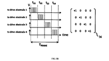
- the capacitances of all mutual capacitors in the electrode array are measured according to a driving sequence, the timing diagram for which is shown in FIG. 3b.
- a single frame period (T FRAME ) consists of four measurement periods (t S1 , t S2 , t S3 and t S4 ).
- the same voltage excitation signal is applied to the drive electrodes one by one, such that during the first measurement period the voltage excitation signal is applied to the first electrode, during the second measurement period the same voltage excitation signal is applied to the second drive electrode, and so on.
- the sequence starts from the beginning to obtain the data for the next frame of operation.
- the patterns of voltage excitation signals applied during one frame of operation may be represented as a matrix 36, which is an identity matrix in this example.
- the accuracy of the estimation of the location of the conductive object may be improved by increasing the signal-to-noise ratio (SNR) associated with the measurement of the capacitance of the mutual coupling capacitors in the array.
- SNR signal-to-noise ratio
- a known method of increasing the SNR of a system that employs projected capacitance sensing method is disclosed, for example, in US20100060591 (Yousefpor, filed September 10, 2008 and published March 11, 2010). According to this method, all of the drive electrodes are excited simultaneously during the measurement period. Each drive electrode is supplied with one of two (or more) possible types of signal that differ from each other in amplitude or phase or both.
- FIG. 4 A timing diagram for an alternative driving sequence is shown in FIG. 4.
- the capacitances of all mutual capacitors in the electrode array are measured during one frame period (T FRAME ) that consists of four measurement periods (t S1 , t S2 , t S3 and t S4 ).
- T FRAME one frame period
- voltage excitation signals are applied to all drive electrodes of the electrode array and the currents generated in the sense electrodes are measured.
- the patterns of voltage excitation signals applied to the drive electrodes are different during each measurement period.
- the patterns of voltage excitation signals applied during one frame of operation may be represented as a matrix 41.
- a limitation of this method is that the current measurement means 24 may saturate whilst making the capacitance measurements.
- the capacitance of the mutual capacitors may comprise a portion that changes due to the presence of an object and fixed offset that is insensitive to presence of an input object.
- the offset signal also known as the baseline signal may be significantly larger than the maximum change signal. Saturation may arise in the current measurement means due to the presence of the large baseline capacitance signal. As a result, the dynamic range of the sensor may be reduced and the performance of the touch panel may be degraded.
- a known solution to the problem described above is to excite the drive electrodes in a pattern corresponding to a maximum length sequence, or M-sequence.
- M-sequence a maximum length sequence
- US8730197 Hamaguchi, filed January 23, 2012 and issued May 20, 2014.
- this method is not suitable for touch panels where the number of drive electrodes is not equal to 2 n - 1.
- a means is therefore sought to operate the touch panel in such a way as to maximize the signal-to-noise ratio of the capacitance measurement without negatively impacting the dynamic range.
- a capacitive touch sensor includes: an array of electrode elements, each electrode element including a drive electrode and a sense electrode, the drive electrode and the sense electrode forming at least one mutual coupling capacitor in each electrode element; and a controller operatively coupled to the array of electrode elements, the controller configured to provide excitation signals to the array of electrode elements over at least one measurement period, and to measure the at least one mutual coupling capacitance over the at least one measurement period, wherein the excitation signals applied during the at least one measurement period are balanced to reduce the effect of baseline capacitance.
- the signal-to-noise ratio and dynamic range of conventional capacitive touch screens present problems when using touch screen to detect a position of an object over, but not touching, the touch screen. Therefore, a means is sought to operate the touch panel in such a way as to maximize the signal-to-noise ratio of the capacitance measurement without negatively impacting the dynamic range.
- the capacitive touch panel can include an array of electrode elements with each electrode element including at least one drive electrode and one sense electrode.
- Mutual coupling capacitors are formed between the drive electrode and sense electrode in each electrode element.
- the capacitance of the mutual coupling capacitors may change due to the presence of an input object in close proximity to the surface of the touch panel.
- the capacitance of a mutual coupling capacitor without the presence of an input object known as the baseline capacitance, may be significantly larger than the change in capacitance caused by the input object.
- the apparatus in accordance with the present invention can minimize or eliminate unwanted baseline capacitance signals. As a result it is possible to create a touch sensor with a high signal-to-noise ratio (SNR) and a large dynamic range.
- SNR signal-to-noise ratio
- FIG. 1 shows a typical implementation of a surface capacitance type touch panel.
- FIG. 2 shows a typical implementation of a projected capacitance type touch panel.
- FIG. 3A shows a schematic representation of a mutual capacitive touch panel system according to the prior art.
- FIG. 3B shows a mathematical representation of a known measurement method for a capacitive touch panel.
- FIG. 4 shows a mathematical representation of an alternative known measurement method for a capacitive touch panel.
- FIG. 5 shows a schematic representation of a mutual capacitive touch panel system according to a first embodiment.
- FIG. 6 shows reduction of dimensionality of an exemplary drive matrix of size 8x8 down to the drive matrix of size 7x7.
- FIG. 7 shows reduction of dimensionality of an exemplary drive matrix of size 7x7 down to the drive matrix of size 6x6.
- FIG. 8A shows an exemplary sensor substrate with an array of electrode elements in accordance with the present invention.
- FIG. 8B shows a plan view of one electrode element of the array of electrode elements.
- FIG. 8C shows a cross section of the sensor substrate.
- FIG. 9A shows an exemplary circuit that is able to measure a signal generated on a sense electrode.
- FIG. 9B shows an exemplary timing diagram that may be used to operate the circuit of FIG. 9A.
- FIG. 9C shows an exemplary system that makes use of the touch sensor.
- FIG. 10A shows a schematic representation of an array of electrode elements according to the second and third embodiments.
- FIG. 10B shows a plan view of an exemplary electrode element with more than one drive electrode.
- FIG. 10C shows a matrix representation of capacitances of an array of electrode elements.
- FIG. 11 shows the a mathematical representation of a measurement procedure in accordance with a second embodiment of the invention.
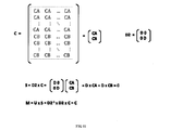
- FIG. 12 shows the form of the drive matrix D3, as well as theoretical expressions for signal matrix S and capacitance matrix C according to the third embodiment.
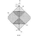
- FIG. 13 shows a plan view of an exemplary electrode element with more than one sense electrode.
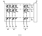
- FIG. 14 shows a schematic diagram of interconnection between sense electrodes and sense unit according to the fourth embodiment.
- the present invention provides a touch panel, or touch sensor, device which overcomes one or more of the aforementioned limitations of the prior art and provides a means of minimizing, or eliminating, the unwanted baseline capacitance signals. As a result it is possible to create a touch sensor with a high signal-to-noise ratio (SNR) and a large dynamic range.
- SNR signal-to-noise ratio
- the capacitive touch panel includes an array of electrode elements with each electrode element including at least one drive electrode and one sense electrode.
- Mutual coupling capacitors are formed between the drive electrode and sense electrode in each electrode element.
- the capacitance of the mutual coupling capacitors may change due to the presence of an input object in close proximity to the surface of the touch panel.
- the input object may be, for example, a finger or a pen, or a stylus or the like.
- the capacitance of a mutual coupling capacitor without the presence of an input object known as the baseline capacitance, may be significantly larger than the change in capacitance caused by the input object.
- Voltage excitation signals are applied to the drive electrodes and the resulting signals generated on the sense electrodes may be measured and used to determine the capacitance of the mutual coupling capacitors. Examination of the capacitance changes of the mutual coupling capacitors provides information about the presence and location of one or more input objects.
- the capacitances of the mutual coupling capacitors are measured during one frame period that consists of multiple measurement periods.
- voltage excitation signals are applied to multiple drive electrodes simultaneously.
- Each drive electrodes in the array may be excited by a first voltage excitation signal, a second voltage excitation signal or held at a constant voltage.
- the first voltage excitation signal and second voltage excitation signal may differ from each other in amplitude, or in polarity or in phase. Further, the voltage excitation signals applied during one measurement period may be balanced.
- Each row of matrix D represents the pattern of the excitation signals applied to the drive electrodes at one particular measurement period.
- Each column represents the pattern of excitation signals applied to one particular drive electrode over the course of a single frame of operation.
- Each element of the array is either equal to 1 or -1 representing application of the first voltage signal or second voltage signal respectively.
- the drive matrix may be chosen so that the sum of each row of the drive matrix is minimized such that it is equal to, or close to, zero. Accordingly, the baseline capacitances of the mutual coupling capacitors in the array do not contribute to the signal measured on the sense electrodes. The changes in capacitance of the mutual capacitors of the array that represent the presence of input objects may therefore be measured with maximum SNR and with maximum dynamic range.
- a touch sensor in accordance with the present invention includes a sensor substrate, and an array of electrode elements formed over the sensor substrate.
- Each electrode element of the array includes at least one drive electrode and at least one sense electrode.
- the at least one drive electrode and at least one sense electrode form at least one mutual coupling capacitor in each electrode element.
- the capacitances of the mutual coupling capacitors across the array may be measured and used in combination to detect the presence and location of input objects touching the surface of the touch panel. For example, the capacitances of the mutual capacitors may change in magnitude when an object is brought into close proximity to the corresponding electrode element.
- a controller may be operatively coupled to the array of electrode elements and configured to determine the object position based on these changes in the multiple mutual coupling capacitors.
- voltage excitation signals are applied to the drive electrodes of the electrode array and the currents generated in the sense electrodes are measured.
- Multiple drive electrodes may be excited during the measurement period by a first periodic voltage excitation signal with a first phase and first amplitude or a second periodic voltage excitation signal with a second phase and second amplitude.
- the capacitances of all mutual capacitors in the electrode array may be measured during one frame of operation that may consist of multiple measurement periods.
- the patterns of voltage excitation signals applied to the drive electrodes may be different during each measurement period.
- the patterns of voltage excitation signals applied during one frame of operation may be represented as a matrix, herein referred to as the drive matrix.
- the corresponding measurements of sense electrode currents during one frame of operation may also be represented as a matrix, herein referred to as the sense matrix.
- the drive matrix In order for each of the capacitances in the electrode array to be uniquely estimated from the multiplicity of sense electrode current measurements the drive matrix must be invertible. In order to supress the unwanted offset, or baseline, signal measured by the controller, the pattern of voltage excitation signals applied during each measurement period of the frame period must be balanced. That is to say, the number of drive electrodes excited by the first voltage excitation signal should be equal, or nearly equal, to the number of drive electrodes excited by the second voltage excitation signal. As used herein, nearly equal to the number of drive electrodes means that a difference between the number of drive electrodes excited by the first voltage excitation signal and the number of drive electrodes excited by the second voltage excitation signal is no greater than 10 percent of the total number of drive electrodes. As is now described, this invention describes a method of constructing a drive matrix that minimises the baseline signal for touch sensors with an arbitrary number of drive electrodes.
- a mutual capacitance type touch panel device includes an electrode array 100 comprising a set of drive electrodes 108, which are coupled to a drive unit 102, and a set of sense electrodes 109, which are coupled to a sense unit 104, as shown in FIG. 5.
- Mutual capacitors 105 are formed between each sense electrode 103 of the plurality of sense electrodes and each drive electrode 101 of the plurality of drive electrodes.
- the capacitances of the mutual capacitors formed at the intersections between each drive electrode and each sense electrode in the array can be represented as a single capacitance matrix, C, of dimension NxM where N is the number of drive electrodes in the plurality of drive electrodes, and M is the number of sense electrodes in the plurality of sense electrodes.
- the drive unit 102 comprises a plurality of signal generating circuits 106 each of which is responsible for providing drive excitation signals to one of the drive electrodes of the electrode array.
- the sense unit 104 comprises a plurality of signal sensing circuits 107, each of which is responsible for measuring signal generated on one of the sense electrodes of the electrode array in response to the drive excitation voltage applied to the drive electrodes of the electrode array.
- the capacitances of all mutual capacitors in the electrode array are measured during a frame period (T FRAME ) that consists of multiple measurement periods (t S1 , t S2 , t S3 , ..., t ST ).
- T FRAME frame period
- voltage excitation signals are applied to all drive electrodes of the electrode array and the currents generated in the sense electrodes are measured.
- the drive electrodes are excited during the measurement period by a first periodic voltage excitation signal with a first phase and first amplitude or a second periodic voltage excitation signal with a second phase and equal amplitude.
- the phase of the voltage excitation signals applied in each particular measurement period may be represented as a vector Dv of dimension N.
- the elements of vector Dv are either +1 or -1 and represent voltage excitation signals with a phase of 0 or 180 degrees respectively.
- the amplitude of the voltage excitation signals applied in each particular measurement may be represented as a vector Dv of dimension N.
- the magnitude of the first and second voltage excitation signals may be equal and the elements of vector Dv, which are either +1 or -1, represent the polarity of the excitation signal.
- the voltage excitation signals applied to the drive electrodes over the course of a single frame can be represented as matrix D, of dimension NxT, where T is the number of measurement periods in one frame.
- Each row of matrix D represents the pattern of the excitation signals applied to the drive electrodes at one particular measurement period.
- Each column represents the pattern of excitation signals applied to one particular drive electrode over the course of a single frame of operation.
- the sense matrix S may be represented by the multiplication of the drive matrix D and the capacitance matrix C.
- the change in the element values of the measurement matrix M due to the presence of an input object may be monitored to determine the location of one or more objects touching the surface of the display.
- a balanced drive matrix In order to remove the effect of the baseline signal and therefore maximise signal-to-noise ratio and dynamic range, it is necessary to construct a balanced drive matrix. That is to say, it is necessary to construct a drive matrix in which the sum of every row is equal to, or close to, zero. As used herein, the sum of every row being close to zero means the sum is no greater than 10 percent of the total columns in the matrix. Also, in order to decode the sense matrix S, an additional requirement in the construction of the drive matrix D is that it is invertible.
- the drive matrix may be constructed, for example, by first taking a Hadamard matrix of dimension HxH, where H>N. The dimension of the drive matrix is then reduced to NxN by removing equal number of rows and columns from the drive matrix. The rows and columns selected for removal are those with the longest run of consecutive equal values. If the ith row of the matrix is removed then the ith column of the matrix must also be removed.
- the following example is provided to illustrate the concept of creating a drive matrix of dimension NxN from an original Hadamard matrix of dimension HxH. It will be obvious to those skilled in the art that the value of N and H may be greater or less than the number chosen in this example.
- the required matrix can be constructed by taking a Hadamard matrix of size 8x8 201, as shown in FIG. 6 and removing the row and column with the longest run of consecutive equal values.
- the 1st row 202 and 1st column 203 of the matrix are removed to obtain the required matrix of size 7x7 204 as they contain the longest run of consecutive equal values.
- a new matrix 207 (shown in FIG. 7) of the required size can be obtained by repeating the above procedure twice to remove two rows and two columns. For example an additional row and additional column may be removed from matrix 204 of dimension 7x7 to create a matrix of dimension 6x6.
- the 4th row 206 and 4th column 205 of matrix 204 are removed as they contain the longest runs of consecutive equal values.
- the capacitances of the mutual capacitors are equal to their baseline values. Further, the baseline capacitance values of all mutual capacitors may be the same.
- the sense matrix S for the baseline case is therefore given by:
- FIG 8A and FIG 8B An example of physical construction of an electrode array including the set of drive electrodes 108 and the set of sense electrodes 109 is shown in FIG 8A and FIG 8B.
- Each electrode of the array of electrode elements may be formed on a sensor substrate 304 using standard photolithographic or printing techniques.
- the electrode material may be a transparent conducting material, such as, for example, Indium-Tin Oxide (ITO), Indium Zinc Oxide (IZO) or a conductive polymer.
- the set of drive electrodes 108 is arranged in first direction, for example forming columns of the electrode array 100.
- Each drive electrode 101 in the set of drive electrodes 108 and each sense electrode 103 in the set of sense electrodes 109 are patterned into a series of connected diamonds.
- the drive electrodes 101 and sense electrodes 103 may be patterned as simple rectangular rows and columns or as other tessellating shapes to improve the signal-to-noise ratio (SNR) of the display.
- the drive electrodes 101 may be formed on the substrate 304 in a first layer of transparent conductive material and the sense electrodes 103 formed in a second layer of transparent conductive material above the first layer and separated from it by an electrically insulating layer.
- Such a structure is well-known in the manufacture of capacitive touch panel devices.
- the drive electrodes 101 and sense electrodes 103 may be formed in the same layer of transparent conductive material 307 and an additional metallization layer 306 used to form bridges to interconnect separate regions of the drive electrode 101. Electrical isolation of the drive electrodes 101 from the sense electrodes 103 is achieved by forming an electrically insulating layer 305 between the metallization layer 306 and the layer of transparent conductive material 307.
- a sensing circuit may be used to measure the charge generated on the sense electrodes during a measurement period due to the excitation signals applied to the drive electrodes.
- the generated charge is a function of the mutual capacitances 105 formed at the intersections between drive and sense electrodes and the pattern of drive excitation signals.
- the sensing circuit may be based on a conventional charge-transfer method or may alternatively utilise other known mutual capacitance measurement techniques.
- the schematic diagram of an example sensing circuit 107 suitable for measuring the charge generated on the sense electrodes during a measurement period and using the charge-transfer method is shown in FIG. 9A.
- the sensing circuit 107 may comprise a switching circuit 410, a current integrator circuit 420 and an analogue to digital convertor (ADC) 430.
- ADC analogue to digital convertor
- the switching circuit includes a first sampling switch (S1) 411 that is controlled by a first switch control signal, ⁇ 1 , and a second sampling switches (S2) 412 that is controlled by a second switch control signal, ⁇ 2 .
- the current integrator circuit 420 may be of a well-known design, for example including an operational amplifier 421 with an integration capacitor (C IS ) 422 and a reset switch (S3) 423.
- the reset switch 423 may be controlled by a third switch control signal, ⁇ 3 .
- the touch panel device also includes a drive unit 102 comprising one or more signal generating circuit 106, one per each drive electrode.
- a drive unit 102 comprising one or more signal generating circuit 106, one per each drive electrode.
- the operation of the touch panel device is now described with reference to the schematic diagram of FIG. 9A and the waveform diagram shown in FIG 9B.
- the third switch control signal, ⁇ 3 is made active causing the first reset switch 423 of the current integrator to close.
- the negative input terminal of the operational amplifier 421 is now connected to the output terminal of that operational amplifier and assumes a voltage equal to the reference voltage supplied to the positive terminal of the amplifier, V REF , which may be a fixed constant voltage such as the ground potential.
- the current integrator circuit 420 is now in its reset state.
- the first switch control signal, ⁇ 1 is also made active during the reset period causing the first sampling switch 411 of the switching circuit 410 to close.
- the sense electrode 103 is also reset to the reference voltage, V REF.
- the first and the second sampling switches 411, 412 of the switching circuit 410 are controlled with respect to the voltage excitation signal applied to the drive electrodes 101 by the drive unit 102 to transfer charge from the electrode array to the current integrator circuit 420.
- the sampling stage is divided into a number of sampling cycles.
- the first switch control signal is then activated causing the first sampling switch 411 to close.
- the sense electrode 103 is now connected to the negative input terminal of the operational amplifier 421.
- Each signal generating circuit 106 of the drive unit 102 now changes the voltage of the voltage excitation signal applied to the corresponding drive electrodes 101, which results in the flow of charge through each of the mutual capacitors 105.
- the amount and the direction of the charge flow through a particular mutual capacitor depend on the capacitance of the capacitor and the magnitude and polarity of the voltage change applied to the corresponding drive electrode.
- the total charge flowing into or out of the current integrator circuit 420 equals the algebraic sum of charges that flow through individual mutual capacitors. Therefore, the total charge transferred via the mutual capacitors 105 is integrated onto the integration capacitor 422 and causes the output of the operational amplifier, V OUT to change according to the following formula: where N is the number of drive electrodes, V n is the voltage change applied to n-th drive electrode and C n is the mutual capacitance formed between the sense electrode 103 and n-th drive electrode.
- the first switch control signal, ⁇ 1 is deactivated and the second switch control signal, ⁇ 2 , is made active.
- This causes the second sampling switch 412 to close and the first sampling switch 411 to open, and thereby set the voltage of the sense electrode 103 to be equal to the ground potential, while maintaining the charge accumulated on the integration capacitor 422.
- the signal generating circuits 106 return the voltage of the voltages applied to the drive electrodes of the electrode array to their original potentials. Any charge transferred from the drive electrodes to the sense electrode 103 via the electrode array 100 due to this voltage change is discharged via the second sampling switch 412, while the charge accumulated on the integration capacitor 422 is maintained.
- the final output voltage, V OUT of the differential amplifier is given by where V REF can be a ground potential.
- the analogue to digital converter circuit 430 converts this final differential amplifier output voltage, V OUT , into a digital value, D OUT , suitable for further processing.
- the touch panel device 580 is connected to a host device 590 - for example a mobile phone, Tablet PC or the like - and comprises a sense unit 581, driver unit 582 and an interface unit 583.
- the sense unit 581 may contain the sensor circuits and be connected to the set of sense circuits 109 of the electrode array 100 by connecting wires.
- the sense unit 581 may, for example, contain as many sense circuits 107 as there are sense electrodes in the electrode array 100.
- the drive unit 582 may include the drive circuits that generate the voltage excitation signals and be connected to the set of drive electrodes 108 of the electrode array 100 by connecting wires.
- the drive unit 582 may, for example, contain as many drive circuits 106 as there are drive electrodes in the electrode array 100.
- the interface circuit 583 may generate signals to control the operation of the sense unit 581 and drive unit 582.
- the interface unit 583 may also receive the digital output signals from the sense unit 581, calculate the location of objects touching the surface of the touch panel device from this and communicate this result to the host device 590.
- the host device may then update the image shown on the display device 510 in accordance with the result via a display controller 591. It will be understood by those normally skilled in the art that there are many equivalent arrangements of these components and functions.
- the interface unit 583 may communicate the digital output signals from the sense unit 581 directly to the host device 590 and the host device 590 may calculate the location of objects touching the surface of the touch panel.
- each electrode element in the array may contain more than one drive electrode or more than one sense electrode. Such an arrangement may be useful, for example, to improve the performance of the touch panel or to detect the height of objects above the touch panel surface.
- An array of electrode elements with more than one drive electrode or more than one sense electrode in each electrode element is disclosed in U.S. Application No. 13/435,898 filed on March 30, 2012, which is herein incorporated by reference in its entirety.
- two types of drive electrodes are arranged in such configuration that two drive and one sense electrode are provided at each intersection in the array.
- the electrodes are further arranged such that, for example, a first drive electrode of a drive electrode pair is separated from a sense electrode by a shorter distance, in the plane of the sensor substrate, than a second drive electrode of the drive electrode pair.
- Two separate mutual coupling capacitors are therefore formed in each electrode element, the baseline capacitances of which may not be equal. Accordingly, the existence of mutual coupling capacitors with different baseline values creates a non-zero baseline sense matrix as described above. The dynamic range of the touch panel is therefore reduced.
- a method is provided to create a drive matrix suitable for measuring with high dynamic range the capacitances of an electrode array with more than one drive electrode in each electrode element.
- An exemplary arrangement of electrode array in accordance with the present embodiment is shown schematically in FIG. 10A.
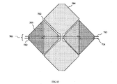
- An exemplary arrangement of an electrode element in accordance with the present embodiment is shown in FIG. 10B.
- the electrode element includes a pair of drive electrodes 601and a sense electrode 604. Different parts of the same drive electrode may be connected by connecting wires 613, 614 and contact holes 612.
- Each drive electrode pair 601 includes a first drive electrode, drive electrode A 602, and a second drive electrode, drive electrode B 603. As shown in FIG.
- each electrode element therefore includes a first mutual coupling capacitor CA formed between drive electrode A and the sense electrode and a second mutual coupling capacitor CB formed between drive electrode B and the sense electrode wherein: the baseline capacitance of the first mutual capacitor CA for each electrode element in the array may be the same; the baseline capacitance of the second mutual capacitor CB for each electrode element in the array may be the same; and the baseline capacitance of the first mutual capacitor CA and the first mutual capacitor CB may be different.
- This matrix is shown in FIG. 10C.
- First half of rows of matrix C contain equal elements CA that represent mutual capacitances between drive electrodes A and sense electrodes of the electrode array, while the second half of rows of matrix C contain equal elements CB that represent mutual capacitances between drive electrodes B and sense electrodes of the electrode array.
- the pattern of excitation signals applied to the drive electrodes A and drive electrodes B over the course of a single frame period can be represented as a drive matrix D2 of dimension 2Nx2N, where N is the number of drive electrodes A, which is also equal to the number of drive electrodes B (and also equal to the number of drive electrode pairs).
- the first half of the columns of drive matrix D2 represents the signals supplied to each of the drive electrodes A 602 over the course of the frame period.
- the first half of the rows of this matrix may represent a first phase of the frame period and the second half of the rows represent a second phase of the frame period.
- the drive electrodes A may be active and the drive electrodes B may be idle.
- the drive electrodes A may be idle and the drive electrodes B may be active. Accordingly, the upper-right and lower-left quadrants of the drive matrix are filled with zeroes, while the upper-left and lower-right quadrants may each be constructed in a similar manner to the drive matrix D of the previous embodiment.
- the form of the drive matrix and the capacitance matrix and the relationship between these and the sense matrix is shown in FIG. 11.
- a limitation of the method described above is that during any given measurement period, only half of the drive electrodes are excited with drive excitation voltages, while the other half of the drive electrodes is idle. This reduces the signal-to-noise ratio of the capacitance measurement to below its maximum achievable value.
- a method is provided to create a drive matrix suitable for measuring with high dynamic range and maximum achievable signal-to-noise ratio the capacitances of an electrode array with more than one drive electrode in each electrode element.
- the present embodiment of this invention utilises the same electrode structure as the one utilised by the second embodiment, however in the present embodiment the drive matrix is constructed in such way that all drive electrodes are supplied with either first or second voltage excitation signal during any given measurement period.
- the drive matrix is constructed in such a way that the baseline signal measured by all sensing circuits during any given measurement period of the frame period, is close to zero when no input object is present in the vicinity of the electrode array, therefore maximising the dynamic range of the system.
- the capacitances of the all mutual capacitors in the array of electrode elements are represented as a single matrix, C of dimension 2NxM, where N is the number of drive electrodes A, which is also equal to the number of drive electrodes B, and M is the number of sense electrodes in the electrode array.
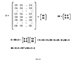
- the first half of rows of matrix C contain elements CA that represent mutual capacitances between drive electrodes A and sense electrodes of the electrode array, while the second half of rows of matrix C contain elements CB that represent mutual capacitances between drive electrodes B and sense electrodes of the electrode array.
- the voltage excitation signals applied to the drive electrodes A and drive electrodes B over the course of a single frame period can be represented as matrix D3 of dimension 2Nx2N, where N is the number of drive electrodes A which is also equal to the number of drive electrodes B.
- the first half of the columns represent the voltage excitation signal applied to the drive electrodes A over the course of the frame period, and the second half of the columns represent the voltage excitation signal applied to the drive electrodes B over the course of the frame period.
- FIG. 12 shows the form of capacitance matrix C and the drive matrix D3, as well as expressions for sense matrix S , the decoding matrix U and the measurement matrix M.
- the baseline capacitances of all first mutual capacitors CA can be assumed to be equal among each other, and the baseline capacitance of all second mutual capacitors CB can be assumed to also be equal among each other. Accordingly, to achieve a baseline sense matrix that is approximately equal to zero, the sum of elements in first half of each row of the drive matrix must be approximately equal to 0, and also the sum of all elements in second half of each row of the drive matrix must be approximately equal to 0. As used herein, the sum of elements in the first half of each row of the drive matrix being approximately equal to 0 means the sum is no greater than 10 percent of the total number of columns in the matrix.
- the drive matrix D3 of the present embodiment may, for example, be constructed by applying a well-known Sylvester type construction method using a primary drive matrix D of dimension NxN as illustrated in FIG. 12.
- the primary drive matrix D may be constructed using the method described previously for the first embodiment of this invention.
- FIG. 13 shows a known arrangement of an electrode element that comprises a sense electrode pair 701 and a drive electrode 704.
- the sense electrode pair further comprises a first sense electrode 702 and a second sense electrode 703. Different parts of the same sense electrode may be connected by connecting wires 713, 714 and contact holes 712.
- a method for measuring with high dynamic range and maximum achievable signal-to-noise ratio the capacitances of an electrode array with more than one sense electrode in each electrode element.
- an array of electrode elements 100 including a set of drive electrodes 108 and sense electrode pairs 701 may be connected to a sense unit 800 which includes a differential sensing apparatus.
- the differential sensing apparatus may include first multiplexer circuits 810, second multiplexer circuits 820 and differential sensing circuits 830.
- the sense electrodes may be connected to the sense unit as illustrated such that the first sense electrodes 702 are connected to the first multiplexing circuits 810 and the second sense electrodes 703 are connected to the second multiplexing circuits 820.
- the at least one measurement period comprises a first measurement period and a second measurement period, and the excitation signal applied during the first measurement period is different from the excitation signal applied during the second measurement period.
- the number of drive electrodes excited by the excitation signal during the first measurement period is substantially the same as the number of drive electrodes excited during the second measurement period.
- the excitation signals comprise at least one of a first voltage signal having a first amplitude and first phase, a second voltage signal having a second amplitude and second phase, or a constant voltage.
- the controller is configured to represent the excitation signals applied to the drive electrodes over one frame as a drive matrix D having dimension NxT, where N is the number of drive electrodes in the array of electrode elements and T is the number of measurement periods in the one frame, each row of the matrix representing a pattern of excitation signals applied to the drive electrodes during a measurement period, and each column of the matrix representing a pattern of excitation signals applied to one drive electrode over the course of a single frame.
- the controller is configured to represent measurements of each sense electrode during the one frame as a sense matrix S having dimension TxM, where M is the number of sense electrodes.
- the controller is configured to determine the capacitances of the mutual coupling capacitors by multiplying the sense matrix S by the inverse of the drive matrix D.
- a first excitation signal is represented in the drive matrix D as a 1 and a second excitation signal is represented in the drive matrix D as a -1, and wherein the drive matrix D is chosen such that the sum of each row of the drive matrix is approximately 0.
- the controller is configured to measure the mutual capacitances in the array during a frame period that includes multiple measurement periods.
- the senor includes: a drive unit coupled to the array of electrode elements, the drive unit configured to provide a drive excitation signal to the drive electrodes of the array of electrode elements, wherein the controller is operatively coupled to the drive unit to cause the drive unit to provide the drive excitation signal to the drive electrodes of the electrode array.
- the drive unit comprises a plurality of signal generating circuits, each signal generating circuit providing a drive excitation signal to a respective drive electrode of the array of electrode elements.
- the senor includes a sense unit coupled to the array of electrode elements, the sense unit configured to measure a signal generated on the sense electrodes in response to the drive excitation signal applied to the drive electrodes
- the sense unit includes a plurality of signal sensing circuits, each signal sensing circuit operative to measure a signal generated on a respective sense electrode of the array of electrode elements in response to the drive excitation signal.
- each electrode of the array of electrode elements comprises a sense electrode and a pair of drive electrodes, the pair of drive electrodes arranged such that a first drive electrode of the pair is adjacent to the sense electrode, and a second drive electrode of the pair is separated from the sense electrode by the first drive electrode.
- the controller is configured to represent the excitation signals applied to the drive electrodes over one frame as a drive matrix D2 having dimension 2Nx2N, where N is the number of drive electrode pairs in the array of electrode elements, and wherein a first half of the columns of the drive matrix D2 represents signals supplied to each first drive electrode over the course of a frame period and a second half of the columns represents signals supplied to each second drive electrode over the course of the frame period, a first half of the rows of the drive matrix D2 represent a first phase of the frame period and a second half of the rows of the drive matrix D2 represent a second phase of the frame period.
- the controller is configured to represent measurements of each sense electrode during the one frame as a sense matrix S having dimension TxM, where T is the number of measurement periods in the one frame and M is the number of sense electrodes.
- the controller is configured to determine the capacitances of the mutual coupling capacitors by multiplying the sense matrix S by the inverse of the drive matrix D2.
- a sum of all elements in a first half of each row of the drive matrix is approximately 0, and a sum of all elements in a second half of each row of the drive matrix is approximately 0.
- the drive matrix is constructed such that all drive electrodes are supplied with a first excitation signal or a second excitation signal during any measurement.
- each electrode element comprises a sense electrode pair, further comprising a differential sensing device operatively coupled to the sense electrode pairs.
- the invention finds application in touch panels and touch-screen devices, for industrial and consumer electronics. It is ideally suited to products such as mobile phones, tablet computers, ‘e-readers,’ and interactive public information terminals.
Landscapes
- Engineering & Computer Science (AREA)
- General Engineering & Computer Science (AREA)
- Theoretical Computer Science (AREA)
- Human Computer Interaction (AREA)
- Physics & Mathematics (AREA)
- General Physics & Mathematics (AREA)
- Position Input By Displaying (AREA)
Abstract
Un capteur tactile capacitif comprend une matrice d'éléments d'électrodes, chaque élément d'électrode comprenant une électrode de commande et une électrode de détection, l'électrode de commande et l'électrode de détection formant au moins un condensateur de couplage mutuel dans chaque élément d'électrode. Un contrôleur est couplé de manière fonctionnelle à la matrice d'éléments d'électrodes, le contrôleur étant conçu pour mesurer au moins une capacité de couplage mutuel sur au moins une période de mesure. De plus, des signaux d'excitation appliqués au cours de ladite au moins une période de mesure sont équilibrés pour réduire l'effet de capacité de ligne de base.
Priority Applications (1)
| Application Number | Priority Date | Filing Date | Title |
|---|---|---|---|
| CN201680018665.2A CN107430464A (zh) | 2015-04-16 | 2016-03-31 | 具有平衡的并联驱动的电容触控面板 |
Applications Claiming Priority (2)
| Application Number | Priority Date | Filing Date | Title |
|---|---|---|---|
| US14/688,666 US9727187B2 (en) | 2015-04-16 | 2015-04-16 | Capacitive touch panel with balanced parallel driving |
| US14/688,666 | 2015-04-16 |
Publications (1)
| Publication Number | Publication Date |
|---|---|
| WO2016166945A1 true WO2016166945A1 (fr) | 2016-10-20 |
Family
ID=57125967
Family Applications (1)
| Application Number | Title | Priority Date | Filing Date |
|---|---|---|---|
| PCT/JP2016/001872 Ceased WO2016166945A1 (fr) | 2015-04-16 | 2016-03-31 | Panneau tactile capacitif à excitation parallèle équilibrée |
Country Status (3)
| Country | Link |
|---|---|
| US (1) | US9727187B2 (fr) |
| CN (1) | CN107430464A (fr) |
| WO (1) | WO2016166945A1 (fr) |
Cited By (1)
| Publication number | Priority date | Publication date | Assignee | Title |
|---|---|---|---|---|
| CN110673756A (zh) * | 2018-09-14 | 2020-01-10 | 友达光电股份有限公司 | 触控显示面板 |
Families Citing this family (19)
| Publication number | Priority date | Publication date | Assignee | Title |
|---|---|---|---|---|
| US10732758B2 (en) * | 2015-11-02 | 2020-08-04 | Neodrón Limited | Touchscreen communication interface |
| TWI567610B (zh) * | 2015-11-13 | 2017-01-21 | Imagination Broadway | Touch Panel Sensing Method and Its Sensing Circuit |
| KR102511952B1 (ko) * | 2016-01-18 | 2023-03-23 | 삼성디스플레이 주식회사 | 터치 스크린 패널 및 그의 구동 방법 |
| US10061375B2 (en) * | 2016-08-02 | 2018-08-28 | Atmel Corporation | Power mode configuration for touch sensors |
| CN106708341B (zh) * | 2016-12-21 | 2024-07-02 | 厦门天马微电子有限公司 | 阵列基板、触控显示面板和触控显示装置 |
| KR102559962B1 (ko) * | 2018-05-02 | 2023-07-26 | 삼성디스플레이 주식회사 | 터치 패널 |
| CN108415623B (zh) * | 2018-05-30 | 2021-01-22 | 京东方科技集团股份有限公司 | 显示基板、显示装置以及获取触控坐标的方法 |
| KR102697626B1 (ko) | 2018-11-12 | 2024-08-26 | 삼성전자주식회사 | 정전식 센서의 커패시턴스 획득 방법 및 정전식 센서 |
| US10691278B1 (en) * | 2019-01-10 | 2020-06-23 | Sharp Kabushiki Kaisha | Reduced line count touch panel for mutual capacitance measurements |
| CN110895293B (zh) * | 2019-12-12 | 2025-05-06 | 深圳芯启航科技有限公司 | 差分式互电容检测电路、方法、芯片及设备 |
| WO2021189443A1 (fr) * | 2020-03-27 | 2021-09-30 | 深圳市汇顶科技股份有限公司 | Circuit de détection de capacité, puce tactile, appareil de détection tactile et dispositif électronique |
| TWI785625B (zh) * | 2020-05-27 | 2022-12-01 | 聯詠科技股份有限公司 | 觸摸感測方法和電子設備 |
| JP7423428B2 (ja) * | 2020-06-05 | 2024-01-29 | シャープ株式会社 | タッチパネル入力装置 |
| US11614839B2 (en) | 2020-08-20 | 2023-03-28 | Apple Inc. | Balanced mutual capacitance systems and methods |
| US11320934B1 (en) | 2020-09-25 | 2022-05-03 | Apple Inc. | System and method for biphase touch sensor panel |
| CN115390703A (zh) * | 2021-05-25 | 2022-11-25 | 矽创电子股份有限公司 | 电容感测装置及其感测方法 |
| CN113777408B (zh) * | 2021-08-19 | 2024-09-27 | 北京他山科技有限公司 | 一种分布式电容传感器系统 |
| CN116459504A (zh) * | 2023-04-28 | 2023-07-21 | 北京他山科技有限公司 | 一种抗干扰低功耗的识别装置 |
| KR102761619B1 (ko) * | 2023-05-26 | 2025-02-03 | 주식회사 하이딥 | 터치 입력 장치 |
Citations (4)
| Publication number | Priority date | Publication date | Assignee | Title |
|---|---|---|---|---|
| US20120013565A1 (en) * | 2010-07-16 | 2012-01-19 | Perceptive Pixel Inc. | Techniques for Locally Improving Signal to Noise in a Capacitive Touch Sensor |
| US20130257786A1 (en) * | 2012-03-30 | 2013-10-03 | Sharp Kabushiki Kaisha | Projected capacitance touch panel with reference and guard electrode |
| WO2013151060A1 (fr) * | 2012-04-04 | 2013-10-10 | シャープ株式会社 | Contrôleur de panneau tactile, circuit intégré, système de panneau tactile et dispositif électronique |
| JP2013246557A (ja) * | 2012-05-24 | 2013-12-09 | Asahi Kasei Electronics Co Ltd | タッチセンサの信号処理回路、およびタッチセンサ |
Family Cites Families (9)
| Publication number | Priority date | Publication date | Assignee | Title |
|---|---|---|---|---|
| US4293734A (en) | 1979-02-23 | 1981-10-06 | Peptek, Incorporated | Touch panel system and method |
| US7663607B2 (en) | 2004-05-06 | 2010-02-16 | Apple Inc. | Multipoint touchscreen |
| US7812827B2 (en) | 2007-01-03 | 2010-10-12 | Apple Inc. | Simultaneous sensing arrangement |
| US9606663B2 (en) | 2008-09-10 | 2017-03-28 | Apple Inc. | Multiple stimulation phase determination |
| US8605054B2 (en) | 2010-09-02 | 2013-12-10 | Texas Instruments Incorporated | Touch-sensitive interface and method using orthogonal signaling |
| JP5079903B1 (ja) | 2011-05-25 | 2012-11-21 | シャープ株式会社 | 静電容量推定方法、集積回路、及び電子機器 |
| JP5231605B2 (ja) | 2011-06-10 | 2013-07-10 | シャープ株式会社 | タッチパネルコントローラ、及びこれを用いた電子機器 |
| US9141239B2 (en) * | 2012-02-07 | 2015-09-22 | Zinitix | Touch screen device, and driving device and driving method for touch panel using predetermined binary sequences |
| US10126883B2 (en) | 2012-07-03 | 2018-11-13 | Sharp Kabushiki Kaisha | Capacitive touch panel with height determination function |
-
2015
- 2015-04-16 US US14/688,666 patent/US9727187B2/en not_active Expired - Fee Related
-
2016
- 2016-03-31 CN CN201680018665.2A patent/CN107430464A/zh active Pending
- 2016-03-31 WO PCT/JP2016/001872 patent/WO2016166945A1/fr not_active Ceased
Patent Citations (4)
| Publication number | Priority date | Publication date | Assignee | Title |
|---|---|---|---|---|
| US20120013565A1 (en) * | 2010-07-16 | 2012-01-19 | Perceptive Pixel Inc. | Techniques for Locally Improving Signal to Noise in a Capacitive Touch Sensor |
| US20130257786A1 (en) * | 2012-03-30 | 2013-10-03 | Sharp Kabushiki Kaisha | Projected capacitance touch panel with reference and guard electrode |
| WO2013151060A1 (fr) * | 2012-04-04 | 2013-10-10 | シャープ株式会社 | Contrôleur de panneau tactile, circuit intégré, système de panneau tactile et dispositif électronique |
| JP2013246557A (ja) * | 2012-05-24 | 2013-12-09 | Asahi Kasei Electronics Co Ltd | タッチセンサの信号処理回路、およびタッチセンサ |
Cited By (2)
| Publication number | Priority date | Publication date | Assignee | Title |
|---|---|---|---|---|
| CN110673756A (zh) * | 2018-09-14 | 2020-01-10 | 友达光电股份有限公司 | 触控显示面板 |
| CN110673756B (zh) * | 2018-09-14 | 2023-06-23 | 友达光电股份有限公司 | 触控显示面板 |
Also Published As
| Publication number | Publication date |
|---|---|
| US20160306456A1 (en) | 2016-10-20 |
| US9727187B2 (en) | 2017-08-08 |
| CN107430464A (zh) | 2017-12-01 |
Similar Documents
| Publication | Publication Date | Title |
|---|---|---|
| WO2016166945A1 (fr) | Panneau tactile capacitif à excitation parallèle équilibrée | |
| US8937607B2 (en) | Capacitive touch panel with dynamically allocated electrodes | |
| US9348470B2 (en) | Projected capacitance touch panel with reference and guard electrode | |
| EP3665555B1 (fr) | Dispositif de traitement de signaux provenant d'un d'un panneau de commande interactif sensible à la pression | |
| KR102719183B1 (ko) | 압력 감지 장치 및 방법 | |
| US9158407B2 (en) | Capacitive touch panel with a ‘dual layer’ force sensor | |
| US11481060B2 (en) | Touch panel pressure detection | |
| US10120478B2 (en) | Piezo based force sensing | |
| KR101735715B1 (ko) | 입력 감지 소자 및 이를 구비한 터치 패널 | |
| JP6290953B2 (ja) | タッチ入力装置 | |
| JP5956989B2 (ja) | 座標位置検出装置 | |
| US9182859B2 (en) | Capacitive touch panel with force sensing | |
| CN101436112B (zh) | 画面输入型图像显示装置 | |
| KR20230003652A (ko) | 압력감지 방식 터치 패널 | |
| CN110199248A (zh) | 具有阵列电极的触摸面板的判别控制器和驱动方法 | |
| CN109669568B (zh) | 带窄边框的有源矩阵触摸面板 | |
| CN103164061B (zh) | 触控感测装置及触控感测设备以及其触控感测方法 | |
| CN109669585B (zh) | 可确定导电类型的电容式触摸感测 | |
| CN108363506B (zh) | 触控显示设备以及用于触控显示面板的方法 | |
| WO2016114123A1 (fr) | Panneau tactile capacitif ayant un motif d'électrode de matrice | |
| KR101613116B1 (ko) | 플렉서블 터치 스크린 패널에 포함되는 터치 검출 장치 |
Legal Events
| Date | Code | Title | Description |
|---|---|---|---|
| 121 | Ep: the epo has been informed by wipo that ep was designated in this application |
Ref document number: 16779744 Country of ref document: EP Kind code of ref document: A1 |
|
| NENP | Non-entry into the national phase |
Ref country code: DE |
|
| 122 | Ep: pct application non-entry in european phase |
Ref document number: 16779744 Country of ref document: EP Kind code of ref document: A1 |