WO2016167218A1 - Corps collé, substrat pour module électrique à dissipateur de chaleur, dissipateur de chaleur, procédé de fabrication de corps collé, procédé de fabrication de substrat pour module électrique à dissipateur de chaleur, et procédé de fabrication de dissipateur de chaleur - Google Patents
Corps collé, substrat pour module électrique à dissipateur de chaleur, dissipateur de chaleur, procédé de fabrication de corps collé, procédé de fabrication de substrat pour module électrique à dissipateur de chaleur, et procédé de fabrication de dissipateur de chaleur Download PDFInfo
- Publication number
- WO2016167218A1 WO2016167218A1 PCT/JP2016/061691 JP2016061691W WO2016167218A1 WO 2016167218 A1 WO2016167218 A1 WO 2016167218A1 JP 2016061691 W JP2016061691 W JP 2016061691W WO 2016167218 A1 WO2016167218 A1 WO 2016167218A1
- Authority
- WO
- WIPO (PCT)
- Prior art keywords
- layer
- heat sink
- metal
- less
- aluminum alloy
- Prior art date
- Legal status (The legal status is an assumption and is not a legal conclusion. Google has not performed a legal analysis and makes no representation as to the accuracy of the status listed.)
- Ceased
Links
Images

Classifications
-
- B—PERFORMING OPERATIONS; TRANSPORTING
- B23—MACHINE TOOLS; METAL-WORKING NOT OTHERWISE PROVIDED FOR
- B23K—SOLDERING OR UNSOLDERING; WELDING; CLADDING OR PLATING BY SOLDERING OR WELDING; CUTTING BY APPLYING HEAT LOCALLY, e.g. FLAME CUTTING; WORKING BY LASER BEAM
- B23K20/00—Non-electric welding by applying impact or other pressure, with or without the application of heat, e.g. cladding or plating
-
- H—ELECTRICITY
- H05—ELECTRIC TECHNIQUES NOT OTHERWISE PROVIDED FOR
- H05K—PRINTED CIRCUITS; CASINGS OR CONSTRUCTIONAL DETAILS OF ELECTRIC APPARATUS; MANUFACTURE OF ASSEMBLAGES OF ELECTRICAL COMPONENTS
- H05K7/00—Constructional details common to different types of electric apparatus
- H05K7/20—Modifications to facilitate cooling, ventilating, or heating
-
- H—ELECTRICITY
- H10—SEMICONDUCTOR DEVICES; ELECTRIC SOLID-STATE DEVICES NOT OTHERWISE PROVIDED FOR
- H10W—GENERIC PACKAGES, INTERCONNECTIONS, CONNECTORS OR OTHER CONSTRUCTIONAL DETAILS OF DEVICES COVERED BY CLASS H10
- H10W40/00—Arrangements for thermal protection or thermal control
- H10W40/10—Arrangements for heating
-
- H—ELECTRICITY
- H10—SEMICONDUCTOR DEVICES; ELECTRIC SOLID-STATE DEVICES NOT OTHERWISE PROVIDED FOR
- H10W—GENERIC PACKAGES, INTERCONNECTIONS, CONNECTORS OR OTHER CONSTRUCTIONAL DETAILS OF DEVICES COVERED BY CLASS H10
- H10W40/00—Arrangements for thermal protection or thermal control
- H10W40/60—Securing means for detachable heating or cooling arrangements, e.g. clamps
-
- H—ELECTRICITY
- H10—SEMICONDUCTOR DEVICES; ELECTRIC SOLID-STATE DEVICES NOT OTHERWISE PROVIDED FOR
- H10W—GENERIC PACKAGES, INTERCONNECTIONS, CONNECTORS OR OTHER CONSTRUCTIONAL DETAILS OF DEVICES COVERED BY CLASS H10
- H10W70/00—Package substrates; Interposers; Redistribution layers [RDL]
- H10W70/60—Insulating or insulated package substrates; Interposers; Redistribution layers
-
- H—ELECTRICITY
- H10—SEMICONDUCTOR DEVICES; ELECTRIC SOLID-STATE DEVICES NOT OTHERWISE PROVIDED FOR
- H10W—GENERIC PACKAGES, INTERCONNECTIONS, CONNECTORS OR OTHER CONSTRUCTIONAL DETAILS OF DEVICES COVERED BY CLASS H10
- H10W70/00—Package substrates; Interposers; Redistribution layers [RDL]
- H10W70/60—Insulating or insulated package substrates; Interposers; Redistribution layers
- H10W70/67—Insulating or insulated package substrates; Interposers; Redistribution layers characterised by their insulating layers or insulating parts
- H10W70/68—Shapes or dispositions thereof
-
- H—ELECTRICITY
- H10—SEMICONDUCTOR DEVICES; ELECTRIC SOLID-STATE DEVICES NOT OTHERWISE PROVIDED FOR
- H10W—GENERIC PACKAGES, INTERCONNECTIONS, CONNECTORS OR OTHER CONSTRUCTIONAL DETAILS OF DEVICES COVERED BY CLASS H10
- H10W90/00—Package configurations
- H10W90/701—Package configurations characterised by the relative positions of pads or connectors relative to package parts
- H10W90/731—Package configurations characterised by the relative positions of pads or connectors relative to package parts of die-attach connectors
- H10W90/734—Package configurations characterised by the relative positions of pads or connectors relative to package parts of die-attach connectors between a chip and a stacked insulating package substrate, interposer or RDL
Definitions
- a metal member made of copper, nickel, or silver is joined to an aluminum alloy member made of an aluminum alloy whose solidus temperature is lower than the eutectic temperature of the metal element constituting the metal member and aluminum.
- a power module substrate with a heat sink including a power module substrate and a heat sink, a heat sink including a heat sink body and a metal member layer, a method for manufacturing the bonded body, and a power module substrate with a heat sink.
- the present invention relates to a manufacturing method and a heat sink manufacturing method.
- Semiconductor devices such as LEDs and power modules have a structure in which a semiconductor element is bonded on a circuit layer made of a conductive material.
- Power semiconductor elements for high power control used for controlling wind power generation, electric vehicles, hybrid vehicles, and the like generate a large amount of heat. Therefore, as a substrate on which a power semiconductor element for high power control is mounted, for example, a ceramic substrate made of AlN (aluminum nitride), Al 2 O 3 (alumina), etc., and one surface of this ceramic substrate has excellent conductivity.
- a power module substrate including a circuit layer formed by bonding metal plates has been widely used.
- a substrate having a metal layer formed on the other surface of a ceramic substrate is also provided.
- a power module substrate in which a circuit layer and a metal layer made of Al are formed on one surface and the other surface of a ceramic substrate, and a solder material is interposed on the circuit layer. And a semiconductor element bonded to each other.
- a heat sink is bonded to the metal layer side of the power module substrate, and heat transferred from the semiconductor element to the power module substrate side is dissipated to the outside through the heat sink.
- Patent Document 2 proposes a technique for joining a circuit layer and a semiconductor element, and a metal layer and a heat sink using a silver oxide paste containing silver oxide particles and a reducing agent made of an organic substance as an alternative to a solder material. ing.
- Patent Document 3 when a circuit layer and a semiconductor element, and a metal layer and a heat sink are bonded using a silver oxide paste, the bonding property between the sintered body of Al and the silver oxide paste is poor. In addition, it is necessary to previously form an Ag underlayer on the circuit layer surface and the metal layer surface. When the Ag underlayer is formed by plating, there is a problem that much labor is required as in the case of Ni plating.
- Patent Document 4 proposes a power module substrate in which a circuit layer and a metal layer have a laminated structure of an Al layer and a Cu layer.
- the Cu layer is disposed on the surface of the circuit layer and the metal layer, the semiconductor element and the heat sink can be favorably bonded using a solder material. For this reason, the thermal resistance in the stacking direction is reduced, and the heat generated from the semiconductor element can be efficiently transmitted to the heat sink side.
- one of the metal layer and the heat sink is made of aluminum or an aluminum alloy, and the other is made of copper or a copper alloy, and the metal layer and the heat sink are solid-phase diffusion bonded.
- a power module substrate with a heat sink has been proposed. In this power module substrate with a heat sink, since the metal layer and the heat sink are solid phase diffusion bonded, the thermal resistance is small and the heat dissipation characteristics are excellent.
- a heat sink having a complicated structure in which a cooling medium flow path or the like is formed may be manufactured by an aluminum casting alloy having a relatively low solidus temperature.
- Patent Document 5 when an aluminum alloy member made of an aluminum cast alloy having a low solidus temperature and a metal member made of copper or a copper alloy are joined by solid phase diffusion bonding, It was confirmed that a lot of Kirkendall voids were generated near the interface due to imbalance of mutual diffusion. When such a Kirkendall void is present between the power module substrate and the heat sink, there is a problem in that the thermal resistance increases and the heat dissipation characteristics deteriorate.
- the present invention has been made in view of the above-described circumstances, and an aluminum alloy member made of an aluminum alloy having a relatively low solidus temperature and a metal member made of copper, nickel, or silver are well bonded.
- the purpose is to do.
- a bonded body includes a metal member made of copper, nickel, or silver, and a solid-state temperature of a metal element that forms the metal member and aluminum.
- An aluminum alloy member made of an aluminum alloy having a temperature lower than the crystallization temperature, wherein the aluminum alloy member and the metal member are solid phase diffusion bonded, and the aluminum alloy member
- the metal member is made of copper or copper alloy, nickel or nickel alloy, or silver or silver alloy.
- the crystal grain aspect ratio (major axis / minor axis) is 2.5 or less and the crystal grain size is 15 ⁇ m or less on the side of the interface between the aluminum alloy member and the metal member. Since a chill layer in which a certain Si phase is dispersed is formed, and the thickness of the chill layer is 50 ⁇ m, the diffusion movement of the metal element constituting the metal member is hindered by this chill layer, and the Kirkendall void Is suppressed, and the thermal resistance in the stacking direction can be lowered.
- a power module substrate with a heat sink includes an insulating layer, a circuit layer formed on one surface of the insulating layer, a metal layer formed on the other surface of the insulating layer, A power module substrate with a heat sink comprising a heat sink disposed on a surface of the metal layer opposite to the insulating layer, wherein the bonding surface of the metal layer to the heat sink is copper, nickel, or
- the joint surface of the heat sink and the metal layer of the heat sink is composed of an aluminum alloy whose solidus temperature is lower than the eutectic temperature of the metal element and aluminum constituting the joint surface of the metal layer.
- the heat sink and the metal layer are solid phase diffusion bonded, and the crystal grain diameter is 2.5 or less on the bonding interface side of the heat sink with the metal layer. 15 ⁇ m are in a chill layer that Si phase is dispersed is formed below, the thickness of the chilled layer is characterized by being the least 50 [mu] m.
- the crystal grain has an aspect ratio (major axis / minor axis) of 2.5 or less and a crystal grain size of 15 ⁇ m or less on the bonding interface side with the metal layer in the heat sink.
- a chill layer in which the Si phase is dispersed is formed, and the thickness of the chill layer is 50 ⁇ m or more. This chill layer prevents the diffusion movement of the metal elements constituting the metal layer, thereby The generation of kendall voids is suppressed, the thermal resistance is low, and the heat dissipation characteristics are particularly excellent.
- a heat sink according to one aspect of the present invention is a heat sink including a heat sink body and the metal member layer, wherein the metal member layer is made of copper, nickel, or silver, and the heat sink body is a solid phase. It is composed of an aluminum alloy whose linear temperature is lower than the eutectic temperature of the metal element and aluminum constituting the metal member layer, and the crystal grain aspect is formed on the bonding interface side of the heat sink body with the metal member layer.
- Si having an aspect ratio (major axis / minor axis) of crystal grains of 2.5 or less and a crystal grain diameter of 15 ⁇ m or less is formed on the bonding interface side with the metal member layer in the heat sink body.
- a chill layer in which phases are dispersed is formed, and the thickness of the chill layer is 50 ⁇ m or more. This chill layer prevents the diffusion movement of the metal element constituting the metal member layer, and the Kirkendall void. Is suppressed, the thermal resistance is low, and the heat dissipation characteristics are particularly excellent.
- a metal member made of copper, nickel, or silver, and a solidus temperature is set to be lower than a eutectic temperature of the metal element constituting the metal member and aluminum.
- the crystal grain has an aspect ratio of 2.5 or less and a crystal grain size of 15 ⁇ m or less on the joint surface side with the metal member.
- a chill layer in which the Si phase is dispersed and the thickness of the chill layer is 80 ⁇ m or more, it is possible to suppress the metal element constituting the metal member from diffusing and moving more than necessary during solid phase diffusion bonding, Generation of Kirkendall void can be suppressed.
- the metal element constituting the metal member is diffused into a part of the chill layer during solid phase diffusion bonding to form a diffusion bonding layer.
- the thickness of the chill layer may be smaller than the thickness of the chill layer before bonding.
- the aluminum alloy member and the metal member are laminated, and the aluminum alloy member and The metal member is preferably solid phase diffusion bonded.
- the temperature rise rate can be increased, and solid phase diffusion bonding can be performed in a relatively short time. It becomes. Thereby, even when it joins in air
- a method for manufacturing a power module substrate with a heat sink includes an insulating layer, a circuit layer formed on one surface of the insulating layer, and a metal layer formed on the other surface of the insulating layer. And a heat sink disposed on a surface of the metal layer opposite to the insulating layer, and a method for manufacturing a power module substrate with a heat sink, wherein the bonding surface of the metal layer to the heat sink is Copper, nickel, or silver, and the joining surface of the heat sink with the metal layer has a solidus temperature less than the eutectic temperature of the metal element and aluminum constituting the joining surface of the metal layer.
- the crystal grain has an aspect ratio of 2.5 or less and a crystal grain size of 15 ⁇ m or less on the joint surface side with the metal layer.
- the thickness of the chilled layer of not less than 80 [mu] m, and a and the heat sink the metal layer characterized by solid-phase diffusion bonding.
- the crystal grain has an aspect ratio of 2.5 or less and a crystal grain size of 15 ⁇ m or less on the bonding surface side with the metal layer.
- the chill layer having a Si phase dispersed therein is formed and the thickness of the chill layer is 80 ⁇ m or more, the metal element constituting the bonding surface of the metal layer diffuses and moves more than necessary during solid phase diffusion bonding. This can be suppressed, and the generation of Kirkendall void can be suppressed. Therefore, it is possible to manufacture a power module substrate with a heat sink having a low thermal resistance in the stacking direction and excellent heat dissipation characteristics.
- the heat sink and the metal layer are laminated, and heated and heated while being pressed in the laminating direction. It is preferable to perform solid phase diffusion bonding with the metal layer.
- the rate of temperature rise can be increased, and solid phase diffusion bonding can be performed in a relatively short time. . Thereby, even when bonded in the atmosphere, for example, the influence of oxidation on the bonding surface is small, and the heat sink and the metal layer can be bonded well.
- a heat sink manufacturing method is a heat sink manufacturing method including a heat sink body and the metal member layer, wherein the metal member layer is made of copper, nickel, or silver,
- the heat sink body is made of an aluminum alloy whose solidus temperature is lower than the eutectic temperature of the metal element and aluminum constituting the metal member layer.
- the metal member layer and A chill layer in which a Si phase having a crystal grain aspect ratio of 2.5 or less and a crystal grain size of 15 ⁇ m or less is dispersed, and the thickness of the chill layer is 80 ⁇ m or more.
- the main body and the metal member layer are solid-phase diffusion bonded.
- the crystal grains in the heat sink body before bonding, on the bonding surface side with the metal member layer, the crystal grains have an aspect ratio of 2.5 or less and a crystal grain size of 15 ⁇ m or less. While forming a chill layer in which phases are dispersed, and the thickness of the chill layer is 80 ⁇ m or more, it is possible to prevent the metal element constituting the metal member layer from diffusing and moving more than necessary during solid phase diffusion bonding, Generation of Kirkendall void can be suppressed. Therefore, it is possible to manufacture a heat sink having low heat resistance in the stacking direction and excellent heat dissipation characteristics.
- the heat sink body and the metal member layer are laminated, and heated and energized while being pressed in the laminating direction. It is preferable to perform solid phase diffusion bonding with the member layer.
- the heat sink body and the metal member layer are energized and heated while being pressed in the stacking direction, so that the rate of temperature rise can be increased and solid phase diffusion bonding can be performed in a relatively short time. It becomes. Thereby, even when it joins in air
- an aluminum alloy member made of an aluminum alloy having a relatively low solidus temperature and a metal member made of copper, nickel, or silver are well bonded, and a bonded body having a low thermal resistance in the stacking direction, It becomes possible to provide a power module substrate with a heat sink and a heat sink, and a manufacturing method of the bonded body, a manufacturing method of the power module substrate with a heat sink, and a manufacturing method of the heat sink.
- FIG. 1 It is a schematic explanatory drawing of the power module provided with the board
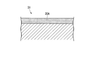
- FIG. 5 is a cross-sectional enlarged explanatory view of a joining surface portion of a heat sink before joining in the method for manufacturing a power module substrate with a heat sink shown in FIG. 4. It is a schematic explanatory drawing of the heat sink which concerns on 2nd embodiment of this invention.
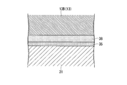
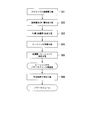
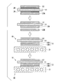
- FIG. 7 is a cross-sectional enlarged explanatory view of a joining interface between a heat sink body and a metal member layer of the heat sink shown in FIG. 6. It is a flowchart explaining the manufacturing method of the heat sink which concerns on 2nd embodiment. It is a schematic explanatory drawing of the manufacturing method of the heat sink which concerns on 2nd embodiment.
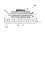
- FIG. 1 the power module 1 using the board
- the power module 1 includes a power module substrate 30 with a heat sink, and a semiconductor element 3 bonded to one surface (the upper surface in FIG. 1) of the power module substrate 30 with a heat sink via a solder layer 2.
- the power module substrate 30 with a heat sink includes a power module substrate 10 and a heat sink 31 bonded to the power module substrate 10.
- the power module substrate 10 is disposed on the ceramic substrate 11 constituting the insulating layer, the circuit layer 12 disposed on one surface (the upper surface in FIG. 1) of the ceramic substrate 11, and the other surface of the ceramic substrate 11. And a metal layer 13 provided.
- the ceramic substrate 11 is made of ceramics such as Si 3 N 4 (silicon nitride), AlN (aluminum nitride), and Al 2 O 3 (alumina) that are excellent in insulation and heat dissipation.
- the ceramic member 11 is made of AlN (aluminum nitride) that is particularly excellent in heat dissipation.
- the thickness of the ceramic substrate 11 is set within a range of 0.2 mm to 1.5 mm, for example, and is set to 0.635 mm in the present embodiment.
- the circuit layer 12 is formed by joining an aluminum plate 22 made of aluminum or an aluminum alloy to one surface of the ceramic substrate 11.
- the circuit layer 12 is formed by joining an aluminum (2N aluminum) rolled plate (aluminum plate 22) having a purity of 99% by mass or more to the ceramic substrate 11.
- the thickness of the aluminum plate 22 used as the circuit layer 12 is set in the range of 0.1 mm or more and 1.0 mm or less, and is set to 0.6 mm in this embodiment.
- the metal layer 13 is laminated on the Al layer 13A disposed on the other surface of the ceramic substrate 11 and on the surface of the Al layer 13A opposite to the surface to which the ceramic substrate 11 is bonded.
- Cu layer 13B As shown in FIG. 4, the Al layer 13 ⁇ / b> A is formed by bonding an aluminum plate 23 ⁇ / b> A made of aluminum or an aluminum alloy to the other surface of the ceramic substrate 11.
- the Al layer 13A is formed by joining an aluminum (2N aluminum) rolled plate (aluminum plate 23A) having a purity of 99% by mass or more to the ceramic substrate 11.
- the thickness of the aluminum plate 23A to be joined is set within a range of 0.1 mm or more and 3.0 mm or less, and is set to 0.6 mm in this embodiment.
- the Cu layer 13B is formed by bonding a copper plate 23B made of copper or a copper alloy to the other surface of the Al layer 13A.
- the Cu layer 13B is formed by bonding an oxygen-free copper rolled plate (copper plate 23B).
- the thickness of the copper layer 13B is set within a range of 0.1 mm to 6 mm, and is set to 1 mm in this embodiment.
- the heat sink 31 is for dissipating heat on the power module substrate 10 side, and in the present embodiment, as shown in FIG. 1, a flow path 32 through which a cooling medium flows is provided.
- This heat sink 31 is made of a cast material of an aluminum alloy whose solidus temperature is less than the eutectic temperature (548 ° C.) of Cu and Al constituting the bonding surface (Cu layer 13B) of the metal layer 13. .
- it is made of a cast material of ADC12 (solidus temperature 515 ° C.) which is an aluminum alloy for die casting containing Si specified in JIS H 2118: 2006.
- the ADC 12 is an aluminum alloy containing Cu in a range of 1.5 mass% to 3.5 mass% and Si in a range of 9.6 mass% to 12.0 mass%.
- the Si content in the cast aluminum alloy is preferably 1% by mass to 25% by mass, but is not limited thereto.
- the heat sink 31 has a crystal grain aspect ratio (major axis / minor axis) of 2.5 or less and a crystal grain size of 15 ⁇ m or less on the side of the joint interface with the metal layer 13 (Cu layer 13B).
- a chill layer 35 in which the Si phase is dispersed is formed.
- the aspect ratio (major axis / minor axis) of the crystal grains of the Si phase is preferably 1.0 or more and 2.0 or less, more preferably 1.0 or more and 1.5, and the crystal grain size is preferably 0.00. Although it is 5 micrometers or more and 10 micrometers or less, More preferably, they are 1 micrometer or more and 7 micrometers or less, However It is not limited to this.
- the chill layer 35 is formed on a surface layer portion (a portion in the vicinity of the mold) of the cast material when the cast material constituting the heat sink 31 is formed. Compared with the inside of the cast material, the chill layer 35 has a crystal grain size. It is fine and has a small aspect ratio. And the thickness (thickness of the chill layer after joining) of the chill layer 35 of the power module substrate 30 with a heat sink is 50 ⁇ m or more. The thickness of the chill layer 35 is preferably 100 ⁇ m or more, more preferably 200 ⁇ m or more, but is not limited thereto.
- the heat sink 31 and the metal layer 13 are solid phase diffusion bonded.
- an intermetallic compound layer 38 is formed at the bonding interface between the metal layer 13 (Cu layer 13 ⁇ / b> B) and the heat sink 31. That is, the intermetallic compound layer 38 is laminated on the chill layer 35 of the heat sink 31.
- the intermetallic compound layer 38 is formed by mutual diffusion of Al atoms of the heat sink 31 and Cu atoms of the Cu layer 13B.
- This intermetallic compound layer 38 has a concentration gradient in which the concentration of Al atoms gradually decreases and the concentration of Cu atoms increases as it goes from the heat sink 31 to the Cu layer 13B.
- the intermetallic compound layer 38 is composed of an intermetallic compound composed of Cu and Al.
- the intermetallic compound layer 38 has a structure in which a plurality of intermetallic compounds are stacked along the bonding interface.
- the thickness of the intermetallic compound layer 38 is set in the range of 1 ⁇ m to 80 ⁇ m, preferably in the range of 5 ⁇ m to 80 ⁇ m.
- the intermetallic compound layer 38 is formed by diffusing Cu of the Cu layer 13B toward the heat sink 31 (chill layer 35), and the intermetallic compound layer 38 includes Si contained in the heat sink 31. The particles are dispersed.
- the intermetallic compound layer 38 has a structure in which three kinds of intermetallic compounds are laminated, and the heat sink 31 and the Cu layer 13B are joined in order from the heat sink 31 side to the Cu layer 13B side.
- a ⁇ phase and a ⁇ 2 phase are stacked along the interface, and at least one of a ⁇ 2 phase, a ⁇ phase, and a ⁇ 2 phase is stacked.
- oxides are dispersed in layers along the bonding interface at the bonding interface between the intermetallic compound layer and the Cu layer 13B.
- this oxide is an aluminum oxide such as alumina (Al 2 O 3 ).
- the oxide is dispersed in a state of being divided at the interface between the intermetallic compound layer and the Cu layer 13B, and there is a region where the intermetallic compound layer and the Cu layer 13B are in direct contact.
- the oxide is dispersed in layers within at least one of the ⁇ phase, ⁇ 2 phase, or ⁇ 2 phase, ⁇ phase, and ⁇ 2 phase.
- an aluminum plate 22 to be the circuit layer 12 is laminated on one surface of the ceramic substrate 11 with an Al—Si brazing material foil 26 interposed therebetween. Further, an aluminum plate 23A to be the Al layer 13A is laminated on the other surface of the ceramic substrate 11 with an Al—Si based brazing material foil 26 interposed therebetween. In this embodiment, an Al-8 mass% Si alloy foil having a thickness of 10 ⁇ m is used as the Al—Si brazing material foil 26.
- circuit layer and Al layer forming step S02 Then, the aluminum plate 22 and the ceramic substrate 11 are joined by placing and heating in a vacuum heating furnace under pressure in the laminating direction (pressure 1 to 35 kgf / cm 2 (0.10 to 3.43 MPa)). The circuit layer 12 is formed. Further, the ceramic substrate 11 and the aluminum plate 23A are joined to form the Al layer 13A.
- the pressure in the vacuum heating furnace is set in the range of 10 ⁇ 6 Pa to 10 ⁇ 3 Pa
- the heating temperature is set to 600 ° C. to 650 ° C.
- the holding time is set in the range of 30 minutes to 180 minutes. It is preferable.
- a copper plate 23B to be the Cu layer 13B is laminated on the other surface side of the Al layer 13A.
- the Al layer 13A and the copper plate 23B are solid-phase diffused by placing them in a vacuum heating furnace under pressure in the stacking direction (pressure 3 to 35 kgf / cm 2 (0.29 to 3.43 MPa)).
- the metal layer 13 is formed by bonding.
- the pressure in the vacuum heating furnace is set within the range of 10 ⁇ 6 Pa to 10 ⁇ 3 Pa
- the heating temperature is set to 400 ° C. to 548 ° C.
- the holding time is set within the range of 5 minutes to 240 minutes. It is preferable.
- each surface of the Al layer 13A and the copper plate 23B to be solid-phase diffusion bonded is previously smoothed by removing scratches on the surfaces.
- a heat sink 31 to be joined is prepared.
- the crystal grain has an aspect ratio of 2.5 or less and a crystal grain size of 15 ⁇ m or less on the side of the heat sink 31 where the metal layer 13 (Cu layer 13B) is joined.
- the chill layer 35A is formed, and the thickness of the chill layer 35A is set to 80 ⁇ m or more.
- the thickness of the chill layer 35A is preferably 100 ⁇ m or more, more preferably 200 ⁇ m or more, but is not limited thereto.
- the thickness of the chill layer 35A described above can be controlled by adjusting the cooling rate of at least the vicinity of the joint surface of the heat sink 31.
- the temperature of the mold during casting is 230 ° C. or lower, preferably 210 ° C. or lower.
- the mold temperature during casting may be 140 ° C. or higher, and preferably 160 ° C. or higher.
- the conditions for casting the heat sink include, for example, a press-fitting pressure of 400 kg / cm 2 to 600 kg / cm 2 , a molten metal temperature of 650 ° C. to 750 ° C., a gate speed of 30 m / s to 60 m / s, and a sleeve filling rate of 40% to 60 %.
- the atmosphere may be an inert atmosphere such as nitrogen or argon, an oxygen atmosphere, a vacuum atmosphere, or the like.
- the thickness of the chill layer 35A can be controlled by adjusting the grinding amount of the surface after casting.
- Metal layer / heat sink bonding step S05 Next, the metal layer 13 (Cu layer 13B) and the heat sink 31 are stacked and pressurized in the stacking direction (pressure 5 to 35 kgf / cm 2 (0.49 to 3.43 MPa)) in a vacuum heating furnace.
- the metal layer 13 (Cu layer 13B) and the heat sink 31 are solid-phase diffusion bonded by arranging and heating.
- each joining surface of the metal layer 13 (Cu layer 13 ⁇ / b> B) and the heat sink 31 to be solid phase diffusion bonded is previously smoothed by removing scratches on the surfaces.
- the pressure during the pressurization is more preferably 8 to 20 kgf / cm 2 (0.78 to 1.96 MPa), but is not limited thereto.
- the pressure in the vacuum heating furnace is in the range of 10 ⁇ 6 Pa to 10 ⁇ 3 Pa
- the heating temperature is 400 ° C. to 520 ° C.
- the holding time is in the range of 0.25 hour to 3 hours.
- the pressure in the vacuum heating furnace is set in the range of 10 ⁇ 5 Pa to 10 ⁇ 4 Pa
- the heating temperature is set to 480 ° C. to 510 ° C.
- the holding time is set in the range of 0.5 hours to 2 hours.
- Cu atoms in the Cu layer 13B diffuse to the chill layer 35A side of the heat sink 31, and as shown in FIG. 2, an intermetallic compound layer 38 and a chill layer 35 are formed. The In this way, the power module substrate with heat sink 30 according to the present embodiment is manufactured.
- semiconductor element bonding step S06 Next, the semiconductor element 3 is laminated on one surface (surface (upper side in FIG. 1)) of the circuit layer 12 via the solder material 2 and soldered in a reduction furnace. As described above, the power module 1 according to the present embodiment is manufactured.
- the heat sink 31 includes Cu and Al whose solidus temperature forms the bonding surface (Cu layer 13B) of the metal layer 13.
- ADC12 solidus temperature 515 ° C.
- the heat sink 31 having a complicated structure having the flow path 32 can be formed, and the heat dissipation performance can be improved.
- the crystal grain aspect ratio (major axis / minor axis) is 2.5 or less and the crystal grain size is 15 ⁇ m or less on the bonding interface side of the heat sink 31 with the metal layer 13 (Cu layer 13B). Since a chill layer 35 in which a certain Si phase is dispersed is formed, and the thickness of the chill layer 35 is 50 ⁇ m or more, diffusion movement of Cu atoms in the metal layer 13 (Cu layer 13B) is caused by the chill layer 35. Can be prevented, and the generation of Kirkendall void can be suppressed. Therefore, even when the power module substrate with heat sink 30 is held at a high temperature, the thermal resistance in the stacking direction does not increase, and deterioration of the heat dissipation characteristics can be suppressed.
- an intermetallic compound layer 38 made of an intermetallic compound layer of Cu and Al is formed at the bonding interface between the metal layer 13 (Cu layer 13B) and the heat sink 31. Since the intermetallic compound layer 38 has a structure in which a plurality of intermetallic compounds are laminated along the bonding interface, the brittle intermetallic compound can be prevented from growing greatly. Further, the volume variation inside the intermetallic compound layer 38 is reduced, and internal strain is suppressed. Further, in the present embodiment, at the bonding interface between the Cu layer 13 ⁇ / b> B and the intermetallic compound layer 38, oxides are dispersed in layers along these bonding interfaces, so that they are formed on the bonding surface of the heat sink 31. Thus, the oxide film is surely broken, and the mutual diffusion of Cu and Al is sufficiently advanced, so that the Cu layer 13B and the heat sink 31 are reliably bonded.
- the bonding to be bonded to the metal layer 13 (Cu layer 13B) in the heat sink 31 in the heat sink preparation step S04, as the heat sink 31 before bonding, the bonding to be bonded to the metal layer 13 (Cu layer 13B) in the heat sink 31.
- the metal layer / heat sink bonding step S05 when the heat sink 31 and the metal layer 13 (Cu layer 13B) are solid phase diffusion bonded, Cu atoms in the Cu layer 13B diffuse and move more than necessary. This can be suppressed, and the generation of Kirkendall void can be suppressed. Therefore, it is possible to manufacture the power module substrate 30 with a heat sink having a low thermal resistance in the stacking direction and excellent heat dissipation characteristics.
- the upper limit of the thickness of the chill layer is not particularly limited, but when the heat sink 31 made of a cast material is used, it is preferably set to 5000 ⁇ m or less. When the heat sink 31 is manufactured by casting, it is difficult to manufacture the heat sink 31 so that the thickness of the chill layer exceeds 5000 ⁇ m. When the heat sink 31 is thin, the entire heat sink 31 may be a chill layer. Even in this case, it is possible to achieve the same effects as the present embodiment.
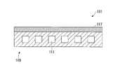
- FIG. 6 shows a heat sink 101 according to the second embodiment of the present invention.
- the heat sink 101 includes a heat sink body 110 and a metal member layer 117 made of copper, nickel, or silver laminated on one surface of the heat sink body 110 (upper side in FIG. 6).
- the metal member layer 117 is configured by joining a metal plate 127 made of an oxygen-free copper rolled plate.
- the heat sink body 110 is provided with a flow path 111 through which a cooling medium flows.
- This heat sink body 110 is made of an aluminum alloy whose solidus temperature is less than the eutectic temperature (548 ° C.) of the metal element (Cu in this embodiment) and Al constituting the metal member layer 117, Specifically, it is made of a cast material of ADC14 (solidus temperature 507 ° C.) which is an aluminum alloy for die casting containing Si specified in JIS H 2118: 2006.
- the ADC 14 is an aluminum alloy containing Si in a range of 16% by mass to 18% by mass and Mg in a range of 0.45% by mass to 0.65% by mass.
- the Si content in the aluminum alloy is preferably 1% by mass to 25% by mass, but is not limited thereto.
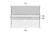
- the heat sink body 110 has a crystal grain aspect ratio (major axis / minor axis) of 2.5 or less and a crystal grain size of 15 ⁇ m or less.
- a chill layer 135 in which a certain Si phase is dispersed is formed.
- the aspect ratio (major axis / minor axis) of the crystal grains of the Si phase is preferably 1.0 or more and 2.0 or less, more preferably 1.0 or more and 1.5, and the crystal grain size is preferably 0.00. Although it is 5 micrometers or more and 10 micrometers or less, More preferably, they are 1 micrometer or more and 7 micrometers or less, However It is not limited to this.
- the chill layer 135 is formed on a surface layer portion (a portion near the mold) of the cast material when forming the cast material constituting the heat sink body 110, and has a crystal grain size as compared with the inside of the cast material. Is fine and has a small aspect ratio.
- the chill layer 135 has a thickness of 50 ⁇ m or more.
- the thickness of the chill layer 135 is preferably 100 ⁇ m or more, more preferably 200 ⁇ m or more, but is not limited thereto.
- the heat sink body 110 and the metal member layer 117 are solid phase diffusion bonded.
- an intermetallic compound layer 138 is formed at the bonding interface between the heat sink body 110 and the metal member layer 117.
- the intermetallic compound layer 138 is formed by mutual diffusion of Al atoms in the heat sink body 110 and Cu atoms in the metal member layer 117.
- the intermetallic compound layer 138 has a concentration gradient in which the Al atom concentration gradually decreases and the Cu atom concentration increases as the heat sink body 110 moves toward the metal member layer 117.
- the intermetallic compound layer 138 is composed of an intermetallic compound composed of Cu and Al.
- the intermetallic compound layer 138 has a structure in which a plurality of intermetallic compounds are stacked along the bonding interface.
- the thickness of the intermetallic compound layer 138 is set in the range of 1 ⁇ m to 80 ⁇ m, preferably in the range of 5 ⁇ m to 80 ⁇ m.
- the intermetallic compound layer 138 is formed by diffusing Cu of the metal member layer 117 toward the heat sink body 110 (chill layer 135), and the intermetallic compound layer 138 includes the heat sink body 110 on the heat sink body 110.
- the Mg particles contained may be dispersed.
- the intermetallic compound layer 138 has a structure in which three kinds of intermetallic compounds are laminated, and the heat sink body 110 and the metal member layer are sequentially arranged from the heat sink body 110 side to the metal member layer 117 side.
- the ⁇ phase and ⁇ 2 phase are laminated along the bonding interface with 117, and at least one of the ⁇ 2 phase, ⁇ phase, and ⁇ 2 phase is laminated.
- the oxide is dispersed in layers along the bonding interface.
- this oxide is an aluminum oxide such as alumina (Al 2 O 3 ).
- the oxide is dispersed in a state of being divided at the interface between the intermetallic compound layer 138 and the metal member layer 117, and there is a region where the intermetallic compound layer 138 and the metal member layer 117 are in direct contact with each other. is doing. In some cases, the oxide is dispersed in layers within at least one of the ⁇ phase, the ⁇ 2 phase, or the ⁇ 2 phase, the ⁇ phase, and the ⁇ 2 phase.
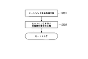
- Heat sink body preparation step S101 First, the heat sink body 110 to be joined is prepared. At this time, the crystal grain aspect ratio is 2.5 or less, similar to the heat sink 31 described in the first embodiment (see FIG. 5), on the bonding surface side of the heat sink body 110 to be bonded to the metal member layer 117.
- the thickness of the chill layer is preferably 100 ⁇ m or more, more preferably 200 ⁇ m or more, but is not limited thereto.
- the thickness of the chill layer can be controlled by adjusting the cooling rate at least in the vicinity of the joint surface of the heat sink body 110.
- the temperature of the mold during casting is 230 ° C. or lower, preferably 210 ° C. or lower.
- the mold temperature during casting may be 140 ° C. or higher, and preferably 160 ° C. or higher.
- the conditions for casting the heat sink include, for example, a press-fitting pressure of 400 kg / cm 2 to 600 kg / cm 2 , a molten metal temperature of 650 ° C.
- the atmosphere may be an inert atmosphere such as nitrogen or argon, an oxygen atmosphere, a vacuum atmosphere, or the like.
- the thickness of the chill layer can be controlled by adjusting the surface grinding amount after casting.
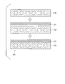
- the heat sink body 110 and the metal plate 127 to be the metal member layer 117 are laminated, and pressure is applied in the laminating direction (pressure 1 to 35 kgf / cm 2 (0.10 to 3.43 MPa).
- pressure is applied in the laminating direction (pressure 1 to 35 kgf / cm 2 (0.10 to 3.43 MPa).
- the metal plate 127 and the heat sink body 110 are solid-phase diffusion bonded by being placed in a vacuum heating furnace and heated.
- each joining surface of the metal plate 127 and the heat sink body 110 to be solid phase diffusion bonded is previously smoothed by removing scratches on the surfaces.
- the pressure during the pressurization is more preferably 8 to 20 kgf / cm 2 (0.78 to 1.96 MPa), but is not limited thereto.
- the pressure in the vacuum heating furnace is in the range of 10 ⁇ 6 Pa to 10 ⁇ 3 Pa
- the heating temperature is 400 ° C. to 520 ° C.
- the holding time is in the range of 0.25 hour to 3 hours. It is preferably set.
- the pressure in the vacuum heating furnace is set in the range of 10 ⁇ 5 Pa to 10 ⁇ 4 Pa
- the heating temperature is set to 480 ° C. to 510 ° C.
- the holding time is set in the range of 0.5 hours to 2 hours.
- Cu atoms in the metal plate 127 diffuse toward the chill layer side of the heat sink body 110, and as shown in FIG. 7, the intermetallic compound layer 138, the chill layer 135, Is formed.
- the heat sink 101 which is this embodiment is manufactured.
- the metal member layer 117 is formed by joining the metal plate 127 made of an oxygen-free copper rolled plate to one surface side of the heat sink body 110. Since it is formed, heat can be spread in the surface direction by the metal member layer 117, and the heat dissipation characteristics can be greatly improved. In addition, other members and the heat sink 101 can be favorably bonded using solder or the like.
- the heat sink body 110 is made of an aluminum alloy whose solidus temperature is less than the eutectic temperature (548 ° C.) of the metal element (Cu) and Al constituting the metal member layer 117, and specifically, Is composed of a cast material of ADC14 (solidus temperature 507 ° C), which is an aluminum alloy for die casting specified in JIS H 2118: 2006. can do.
- the Si phase in which the aspect ratio (major axis / minor axis) of the crystal grains is 2.5 or less and the crystal grain diameter is 15 ⁇ m or less is formed on the bonding interface side with the metal member layer 117 in the heat sink body 110.
- the thickness of the chill layer 135 is 50 ⁇ m or more, the diffusion of Cu atoms in the metal member layer 117 is prevented by the chill layer 135, Generation of Kirkendall void can be suppressed. Therefore, even when the heat sink 101 is held at a high temperature, the thermal resistance in the stacking direction does not increase, and it is possible to suppress deterioration of the heat dissipation characteristics.
- the bonding interface between the metal member layer 117 and the heat sink body 110 has the same configuration as the bonding interface between the Cu layer 13B and the heat sink 31 in the first embodiment. It is possible to achieve the same function and effect.
- the upper limit of the thickness of the chill layer is not particularly limited, but when the heat sink body 110 made of a cast material is used, it is preferably set to 5000 ⁇ m or less. When the heat sink body 110 is manufactured by casting, it is difficult to manufacture the heat sink body 110 so that the thickness of the chill layer exceeds 5000 ⁇ m. When the heat sink body 110 is thin, the entire heat sink body 110 may be a chill layer. Even in this case, it is possible to achieve the same effects as the present embodiment.
- the thickness of the Ni layer is preferably 1 ⁇ m or more and 30 ⁇ m or less. If the thickness of the Ni layer is less than 1 ⁇ m, the effect of improving the reliability of bonding with other members may be lost. If the thickness exceeds 30 ⁇ m, the Ni layer becomes a thermal resistor and heat can be transferred efficiently. There is a risk of disappearing.
- the bonding temperature is set to 400 ° C. or more and 520 ° C. or less for the solid phase diffusion bonding of the Al layer and Ni, but other conditions are the same as in the above-described embodiment. It can be formed under the following conditions.
- the silver oxide of the silver oxide paste is reduced. Since the silver reduced by the agent and the Ag layer to be bonded are bonded between the same kind of metals, the bonding reliability can be improved. Furthermore, since an Ag layer having a good thermal conductivity is formed, heat can be spread efficiently by spreading in the surface direction.
- the thickness of the Ag layer is preferably 1 ⁇ m or more and 20 ⁇ m or less. If the thickness of the Ag layer is less than 1 ⁇ m, the effect of improving the reliability of bonding with other members may be lost.
- the conditions for the solid phase diffusion bonding of the Al layer and Ag are set such that the bonding temperature is 400 ° C. or more and 520 ° C. or less. It can be formed under conditions.
- the metal layer 13 has been described as having the Al layer 13A and the Cu layer 13B.
- the present invention is not limited to this, and as shown in FIG. Or you may comprise with a copper alloy.
- a copper plate is joined to the other surface (lower side in FIG. 10) of the ceramic substrate 11 by the DBC method, the active metal brazing method, or the like.
- a metal layer 213 is formed.
- the metal layer 213 and the heat sink 31 are solid phase diffusion bonded.
- the circuit layer 212 is also made of copper or a copper alloy.
- a power module 201 shown in FIG. 10 includes a power module substrate 230 with a heat sink, and a semiconductor element 3 bonded to one surface (the upper surface in FIG. 10) of the power module substrate 230 with a heat sink via a solder layer 2. It is equipped with.
- the circuit layer is described as being formed by bonding an aluminum plate having a purity of 99% by mass, but is not limited thereto, and pure aluminum having a purity of 99.99% by mass or more, It may be composed of other metals such as aluminum or aluminum alloy, copper or copper alloy.
- the circuit layer may have a two-layer structure of an Al layer and a Cu layer. The same applies to the power module substrate 210 shown in FIG.
- the metal layer 13 (Cu layer 13B) and the heat sink 31 are laminated, placed in a vacuum heating furnace in a state of being pressurized in the lamination direction, and heated.
- the heat sink main body / metal member layer joining step S102 of the second embodiment the heat sink main body 110 and the metal plate 127 to be the metal member layer 117 are stacked and pressurized in the stacking direction (pressure 5 to 35 kgf /
- the present invention is not limited to this, and as shown in FIG.
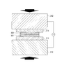
- an electric heating method is used. It may be.
- an aluminum alloy member 301 and a metal member 302 are laminated, and these laminated bodies are laminated by a pair of electrodes 312 and 312 via carbon plates 311 and 311. While pressing in the direction, the aluminum alloy member 301 and the metal member 302 are energized. Then, the carbon plates 311 and 311 and the aluminum alloy member 301 and the metal member 302 are heated by Joule heat, and the aluminum alloy member 301 and the metal member 302 are solid-phase diffusion bonded.
- the rate of temperature increase can be made relatively fast, for example, 30 to 100 ° C./min, and the solid phase can be obtained in a short time. Diffusion bonding can be performed. Thereby, the influence of the oxidation of the bonding surface is small, and for example, bonding can be performed even in an air atmosphere. Further, depending on the resistance value and specific heat of the aluminum alloy member 301 and the metal member 302, it is possible to join the aluminum alloy member 301 and the metal member 302 in a state where a temperature difference is generated, thereby reducing the difference in thermal expansion, Thermal stress can also be reduced.
- the pressure load applied by the pair of electrodes 312 and 312 is set to be within a range of 30 kgf / cm 2 to 100 kgf / cm 2 (2.94 MPa to 9.81 MPa). preferable.
- the pressure load is more preferably 50 kgf / cm 2 or more and 80 kgf / cm 2 or less (4.90 MPa or more and 7.85 MPa or less), but is not limited thereto.
- the surface roughness of the aluminum alloy member 301 and the metal member 302 is 0.3 ⁇ m or more and 0.6 ⁇ m or less in terms of arithmetic average roughness Ra, or 1.
- the surface roughness of the bonding surface is small, but in the case of the electric heating method, if the surface roughness of the bonding surface is too small, the interface contact resistance decreases, and the bonding interface Since it becomes difficult to heat locally, it is preferable to be within the above range.
- the ceramic substrate 11 is an insulator, for example, a jig made of carbon, etc. Therefore, it is necessary to short-circuit the carbon plates 311 and 311.
- the joining conditions are the same as the joining of the aluminum member 301 and the copper member 302 described above.
- the surface roughness of the metal layer 13 (Cu layer 13B) and the heat sink 31 is the same as that of the aluminum member 301 and the copper member 302 described above.
- Example 6-10 an aluminum alloy plate and a metal plate were joined by solid phase diffusion bonding by the electric heating method shown in FIG.
- the pressure load by the electrode was 15 kgf / cm 2 (1.47 MPa)
- the heating temperature was 510 ° C.
- the holding time at the heating temperature was 5 min
- the temperature rising rate was 80 ° C./min.
- the bonding atmosphere was an air atmosphere.
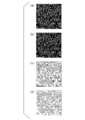
- the thickness of the chill layer formed on the joining surface side was measured as follows. First, using an EPMA (JXA-8530F manufactured by JEOL Ltd.), the surface of the aluminum plate was subjected to Si surface analysis under the conditions of a visual field of 360 ⁇ m ⁇ , an acceleration voltage of 15 kV, and an Si contour level of 0 to 1000. The Si distribution image shown in 12 (a) was obtained. The obtained Si distribution image was converted to an 8-bit gray scale to obtain a Si distribution image as shown in FIG.
- EPMA JXA-8530F manufactured by JEOL Ltd.
- Aspect ratio major axis / minor axis
- Crystal grain size major axis
- the number of particles that do not satisfy the above conditions was determined, and the number of particles that did not satisfy the conditions / conditions was determined.
- measurement was performed every 10 ⁇ m from the surface of the aluminum plate toward the inside of the plate, the number of conditions satisfying the number / number of conditions not satisfying the condition of 3 or more was defined as the chill layer, and the thickness was determined. .
- the evaluation results are shown in Table 1.
- the cross-section of the joined body of the aluminum alloy plate and the metal plate bonded by solid phase diffusion was observed, and the thickness of the chill layer formed at the joint interface was measured as follows.
- the joint interface of the joined body was observed using EPMA (JXA-8530F manufactured by JEOL Ltd.), and the intermetallic compound of Al and the metal elements (Cu, Ni, Ag) of the metal plate grown inside the aluminum alloy plate
- the thickness of the chill layer after joining is obtained by subtracting the thickness of the intermetallic compound of Al and the metal elements (Cu, Ni, Ag) of the metal plate from the thickness of the chill layer before joining. And the thickness.
- the thickness of the intermetallic compound was determined by line analysis of the bonding interface in the thickness direction of the bonded body.
- the Al concentration was 65 at% to 70 at% when copper was used as the metal plate, and nickel was used as the metal plate.
- the thickness was measured by regarding the region of 55 at% to 80 at% as the intermetallic compound when silver was used as the metal plate and the range of 20 at 45 to 45 at% as the metal plate. The evaluation results are shown in Table 1.
- Heat cycle test Next, a heat cycle test was performed on the joined body thus manufactured.
- TSB-51 a thermal shock tester manufactured by Espec Corp.
- test specimen power module with heat sink
- liquid phase Fluorinert
- Comparative Example 1 in which an aluminum alloy plate and a metal plate (copper plate) were solid-phase diffusion bonded without forming a chill layer, it was confirmed that the thermal resistance was higher than that of the present invention. Moreover, when Comparative Example 2 using nickel as the metal plate was compared with Invention Examples 4 and 9, it was confirmed that the thermal resistance of Comparative Example 2 was increased. Similarly, when Comparative Example 3 using silver as a metal plate was compared with Invention Examples 5 and 10, it was confirmed that the thermal resistance of Comparative Example 3 was increased. These are presumed to be due to the formation of Kirkendall void.
- the thermal resistance is smaller than that of the comparative example.
- the thermal resistance is smaller than that of the comparative example.
- an aluminum alloy member made of an aluminum alloy having a relatively low solidus temperature and a metal member made of copper, nickel, or silver are satisfactorily bonded, and the thermal resistance in the stacking direction It was confirmed that it is possible to obtain a bonded body having a low A.
- an aluminum alloy member made of an aluminum alloy having a relatively low solidus temperature and a metal member made of copper, nickel, or silver are well bonded, and a bonded body having a low thermal resistance in the stacking direction, It becomes possible to provide a power module substrate with a heat sink and a heat sink, and a manufacturing method of the bonded body, a manufacturing method of the power module substrate with a heat sink, and a manufacturing method of the heat sink.
Landscapes
- Engineering & Computer Science (AREA)
- Mechanical Engineering (AREA)
- Physics & Mathematics (AREA)
- Thermal Sciences (AREA)
- Microelectronics & Electronic Packaging (AREA)
- Cooling Or The Like Of Semiconductors Or Solid State Devices (AREA)
Abstract
L'invention concerne un corps collé qui est formé par collage d'un organe métallique comprenant du cuivre, du nickel ou de l'argent à un organe en alliage d'aluminium comprenant un alliage d'aluminium dont la température de solidus est inférieure à la température eutectique de l'aluminium et de l'élément métallique qui constitue l'organe métallique. L'organe en alliage d'aluminium et l'organe métallique sont collés par diffusion en phase solide ; une couche de refroidissement, dans laquelle une phase de Si dont les grains cristallins présentent un rapport de forme inférieur ou égal à 2,5 et une dimension de grain cristallin inférieure ou égale à 15 µm est dispersée, est formée côté interface de collage à l'organe métallique de l'organe en alliage d'aluminium ; et l'épaisseur de la couche de refroidissement est configurée pour être supérieure ou égale à 50 µm.
Priority Applications (5)
| Application Number | Priority Date | Filing Date | Title |
|---|---|---|---|
| CN201680022306.4A CN107534034B (zh) | 2015-04-16 | 2016-04-11 | 接合体、自带散热器的功率模块用基板、散热器及接合体的制造方法、自带散热器的功率模块用基板的制造方法、散热器的制造方法 |
| US15/566,817 US10497637B2 (en) | 2015-04-16 | 2016-04-11 | Bonded body, substrate for power module with heat sink, heat sink, method for producing bonded body, method for producing substrate for power module with heat sink, and method for producing heat sink |
| EP16780009.3A EP3285292B1 (fr) | 2015-04-16 | 2016-04-11 | Corps collé, substrat pour module électrique à dissipateur de chaleur, dissipateur de chaleur, procédé de fabrication de corps collé, procédé de fabrication de substrat pour module électrique à dissipateur de chaleur, et procédé de fabrication de dissipateur de chaleur |
| KR1020177029105A KR102422064B1 (ko) | 2015-04-16 | 2016-04-11 | 접합체, 히트 싱크가 부착된 파워 모듈용 기판, 히트 싱크, 및 접합체의 제조 방법, 히트 싱크가 부착된 파워 모듈용 기판의 제조 방법, 히트 싱크의 제조 방법 |
| US15/786,786 US10497585B2 (en) | 2015-04-16 | 2017-10-18 | Bonded body, substrate for power module with heat sink, heat sink, method for producing bonded body, method for producing substrate for power module with heat sink, and method for producing heat sink |
Applications Claiming Priority (4)
| Application Number | Priority Date | Filing Date | Title |
|---|---|---|---|
| JP2015084029 | 2015-04-16 | ||
| JP2015-084029 | 2015-04-16 | ||
| JP2016033201A JP6696214B2 (ja) | 2015-04-16 | 2016-02-24 | 接合体、ヒートシンク付パワーモジュール用基板、ヒートシンク、及び、接合体の製造方法、ヒートシンク付パワーモジュール用基板の製造方法、ヒートシンクの製造方法 |
| JP2016-033201 | 2016-02-24 |
Related Child Applications (2)
| Application Number | Title | Priority Date | Filing Date |
|---|---|---|---|
| US15/566,817 A-371-Of-International US10497637B2 (en) | 2015-04-16 | 2016-04-11 | Bonded body, substrate for power module with heat sink, heat sink, method for producing bonded body, method for producing substrate for power module with heat sink, and method for producing heat sink |
| US15/786,786 Division US10497585B2 (en) | 2015-04-16 | 2017-10-18 | Bonded body, substrate for power module with heat sink, heat sink, method for producing bonded body, method for producing substrate for power module with heat sink, and method for producing heat sink |
Publications (1)
| Publication Number | Publication Date |
|---|---|
| WO2016167218A1 true WO2016167218A1 (fr) | 2016-10-20 |
Family
ID=57126850
Family Applications (1)
| Application Number | Title | Priority Date | Filing Date |
|---|---|---|---|
| PCT/JP2016/061691 Ceased WO2016167218A1 (fr) | 2015-04-16 | 2016-04-11 | Corps collé, substrat pour module électrique à dissipateur de chaleur, dissipateur de chaleur, procédé de fabrication de corps collé, procédé de fabrication de substrat pour module électrique à dissipateur de chaleur, et procédé de fabrication de dissipateur de chaleur |
Country Status (1)
| Country | Link |
|---|---|
| WO (1) | WO2016167218A1 (fr) |
Cited By (2)
| Publication number | Priority date | Publication date | Assignee | Title |
|---|---|---|---|---|
| EP3825118A1 (fr) * | 2019-11-21 | 2021-05-26 | Heraeus Deutschland GmbH & Co KG | Module composé d'échange de chaleur |
| CN113412031A (zh) * | 2021-06-21 | 2021-09-17 | 合肥联宝信息技术有限公司 | 一种升温模组及电子设备 |
Citations (6)
| Publication number | Priority date | Publication date | Assignee | Title |
|---|---|---|---|---|
| JPH04288983A (ja) * | 1991-01-21 | 1992-10-14 | Hakusan Seisakusho:Kk | アルミニウム材と銅材との圧接方法 |
| JP2005103556A (ja) * | 2003-09-26 | 2005-04-21 | Niigata Univ | アルミニウム合金ダイカスト部材の接合方法 |
| JP2009279643A (ja) * | 2008-05-26 | 2009-12-03 | Toyota Central R&D Labs Inc | Al合金ダイカスト鋳物およびその製造方法 |
| JP2011058056A (ja) * | 2009-09-10 | 2011-03-24 | Nissan Motor Co Ltd | アルミニウム合金鋳物部材及びその製造方法 |
| JP2011255389A (ja) * | 2010-06-07 | 2011-12-22 | Furukawa-Sky Aluminum Corp | 金属材料の接合方法 |
| JP2014060215A (ja) * | 2012-09-14 | 2014-04-03 | Mitsubishi Materials Corp | ヒートシンク付パワーモジュール用基板、ヒートシンク付パワーモジュール、及びヒートシンク付パワーモジュール用基板の製造方法 |
-
2016
- 2016-04-11 WO PCT/JP2016/061691 patent/WO2016167218A1/fr not_active Ceased
Patent Citations (6)
| Publication number | Priority date | Publication date | Assignee | Title |
|---|---|---|---|---|
| JPH04288983A (ja) * | 1991-01-21 | 1992-10-14 | Hakusan Seisakusho:Kk | アルミニウム材と銅材との圧接方法 |
| JP2005103556A (ja) * | 2003-09-26 | 2005-04-21 | Niigata Univ | アルミニウム合金ダイカスト部材の接合方法 |
| JP2009279643A (ja) * | 2008-05-26 | 2009-12-03 | Toyota Central R&D Labs Inc | Al合金ダイカスト鋳物およびその製造方法 |
| JP2011058056A (ja) * | 2009-09-10 | 2011-03-24 | Nissan Motor Co Ltd | アルミニウム合金鋳物部材及びその製造方法 |
| JP2011255389A (ja) * | 2010-06-07 | 2011-12-22 | Furukawa-Sky Aluminum Corp | 金属材料の接合方法 |
| JP2014060215A (ja) * | 2012-09-14 | 2014-04-03 | Mitsubishi Materials Corp | ヒートシンク付パワーモジュール用基板、ヒートシンク付パワーモジュール、及びヒートシンク付パワーモジュール用基板の製造方法 |
Cited By (3)
| Publication number | Priority date | Publication date | Assignee | Title |
|---|---|---|---|---|
| EP3825118A1 (fr) * | 2019-11-21 | 2021-05-26 | Heraeus Deutschland GmbH & Co KG | Module composé d'échange de chaleur |
| US11828546B2 (en) | 2019-11-21 | 2023-11-28 | Heraeus Deutschland GmbH & Co. KG | Heat exchange compound module |
| CN113412031A (zh) * | 2021-06-21 | 2021-09-17 | 合肥联宝信息技术有限公司 | 一种升温模组及电子设备 |
Similar Documents
| Publication | Publication Date | Title |
|---|---|---|
| JP6696214B2 (ja) | 接合体、ヒートシンク付パワーモジュール用基板、ヒートシンク、及び、接合体の製造方法、ヒートシンク付パワーモジュール用基板の製造方法、ヒートシンクの製造方法 | |
| KR102422607B1 (ko) | 접합체, 히트 싱크가 부착된 파워 모듈용 기판, 히트 싱크, 및 접합체의 제조 방법, 히트 싱크가 부착된 파워 모듈용 기판의 제조 방법, 히트 싱크의 제조 방법 | |
| KR102154882B1 (ko) | 파워 모듈 | |
| JP6575386B2 (ja) | 接合体の製造方法、ヒートシンク付パワーモジュール用基板の製造方法、及び、ヒートシンクの製造方法 | |
| KR102154369B1 (ko) | 파워 모듈 | |
| JP2016048781A (ja) | 接合体、ヒートシンク付パワーモジュール用基板、ヒートシンク、接合体の製造方法、ヒートシンク付パワーモジュール用基板の製造方法、及び、ヒートシンクの製造方法 | |
| KR102524698B1 (ko) | 접합체, 파워 모듈용 기판, 파워 모듈, 접합체의 제조 방법 및 파워 모듈용 기판의 제조 방법 | |
| US10497585B2 (en) | Bonded body, substrate for power module with heat sink, heat sink, method for producing bonded body, method for producing substrate for power module with heat sink, and method for producing heat sink | |
| WO2016167218A1 (fr) | Corps collé, substrat pour module électrique à dissipateur de chaleur, dissipateur de chaleur, procédé de fabrication de corps collé, procédé de fabrication de substrat pour module électrique à dissipateur de chaleur, et procédé de fabrication de dissipateur de chaleur | |
| JP6673635B2 (ja) | 接合体の製造方法、ヒートシンク付パワーモジュール用基板の製造方法、ヒートシンクの製造方法、及び、接合体、ヒートシンク付パワーモジュール用基板、ヒートシンク | |
| WO2016167217A1 (fr) | Corps lié, substrat pour module d'alimentation pourvu d'un dissipateur thermique, dissipateur thermique, procédé de fabrication de corps lié, procédé de fabrication de substrat pour module d'alimentation pourvu d'un dissipateur thermique, et procédé de fabrication de dissipateur thermique | |
| JP2019087608A (ja) | 接合体、絶縁回路基板、ヒートシンク付絶縁回路基板、ヒートシンク、及び、接合体の製造方法、絶縁回路基板の製造方法、ヒートシンク付絶縁回路基板の製造方法、ヒートシンクの製造方法 | |
| JP6459427B2 (ja) | ヒートシンク付パワーモジュール用基板の製造方法、及び、接合体、ヒートシンク付パワーモジュール用基板、ヒートシンク | |
| TWI753854B (zh) | 接合體之製造方法、附散熱片之電力模組用基板之製造方法、及散熱片之製造方法 |
Legal Events
| Date | Code | Title | Description |
|---|---|---|---|
| 121 | Ep: the epo has been informed by wipo that ep was designated in this application |
Ref document number: 16780009 Country of ref document: EP Kind code of ref document: A1 |
|
| ENP | Entry into the national phase |
Ref document number: 20177029105 Country of ref document: KR Kind code of ref document: A |
|
| WWE | Wipo information: entry into national phase |
Ref document number: 15566817 Country of ref document: US |
|
| NENP | Non-entry into the national phase |
Ref country code: DE |