WO2016174939A1 - Dispositif de détection de rayonnement, dispositif d'imagerie et système d'imagerie - Google Patents
Dispositif de détection de rayonnement, dispositif d'imagerie et système d'imagerie Download PDFInfo
- Publication number
- WO2016174939A1 WO2016174939A1 PCT/JP2016/057474 JP2016057474W WO2016174939A1 WO 2016174939 A1 WO2016174939 A1 WO 2016174939A1 JP 2016057474 W JP2016057474 W JP 2016057474W WO 2016174939 A1 WO2016174939 A1 WO 2016174939A1
- Authority
- WO
- WIPO (PCT)
- Prior art keywords
- radiation detection
- radiation
- detection apparatus
- layer
- substrate
- Prior art date
- Legal status (The legal status is an assumption and is not a legal conclusion. Google has not performed a legal analysis and makes no representation as to the accuracy of the status listed.)
- Ceased
Links
Images











Classifications
-
- A—HUMAN NECESSITIES
- A61—MEDICAL OR VETERINARY SCIENCE; HYGIENE
- A61B—DIAGNOSIS; SURGERY; IDENTIFICATION
- A61B6/00—Apparatus or devices for radiation diagnosis; Apparatus or devices for radiation diagnosis combined with radiation therapy equipment
-
- G—PHYSICS
- G01—MEASURING; TESTING
- G01T—MEASUREMENT OF NUCLEAR OR X-RADIATION
- G01T7/00—Details of radiation-measuring instruments
Definitions
- the present disclosure relates to a radiation detection apparatus, an imaging apparatus, and an imaging system.
- a radiation imaging apparatus that obtains a radiation image by directly detecting radiation without using a radiographic film or the like.
- a radiation imaging apparatus for example, a photoelectric conversion sensor in which a scintillator layer that emits fluorescence upon incidence of radiation is stacked on a light receiving surface is used as a radiation detection element.
- the radiation imaging apparatus it is required for the radiation imaging apparatus to reduce the influence on the subject due to the radiation irradiated at the time of imaging. Therefore, there has been a demand for a radiation imaging apparatus with higher sensitivity that can obtain a clear captured image even with a lower dose of radiation.
- Patent Document 1 when X-rays transmitted through a subject are irradiated from above an X-ray detection element, the X-ray detection element reflects from a member existing below the X-ray detection element and is reflected from the back side.
- a wiring board for mounting an X-ray detection element that shields reflected X-rays that enter the board with a conductor layer or the like is disclosed. According to the wiring board for mounting an X-ray detection element disclosed in Patent Document 1, since the reflected X-rays unrelated to the X-ray transmitted through the subject can be reduced, the X-ray detection element is connected to an external electric circuit. In contrast, a more accurate X-ray image of the subject can be output.
- the present disclosure proposes a new and improved radiation detection apparatus capable of detecting a low dose of radiation, an imaging apparatus including the radiation detection apparatus, and an imaging system including the radiation detection apparatus.
- a substrate including a radiation shielding layer, a plurality of radiation detection elements two-dimensionally arranged on one surface of the substrate, and the other surface of the substrate facing the surface on which the radiation detection elements are arranged are arranged.
- a radiation detection apparatus comprising: at least one circuit element electrically connected to the radiation detection element by a through via penetrating the substrate.
- a substrate including a radiation shielding layer, a plurality of radiation detection elements two-dimensionally arranged on one surface of the substrate, and another surface of the substrate facing the surface on which the radiation detection elements are arranged
- a radiation detection device including at least one circuit element electrically connected to the radiation detection element by a through via penetrating the substrate, and processing an output signal from the radiation detection apparatus Then, an imaging device having an arithmetic processing unit that generates a captured image is provided.
- a substrate including a radiation shielding layer, a plurality of radiation detection elements two-dimensionally arranged on one surface of the substrate, and another surface of the substrate facing the surface on which the radiation detection elements are arranged
- a radiation detection device including at least one circuit element electrically connected to the radiation detection element by a through via penetrating the substrate, and processing an output signal from the radiation detection apparatus Then, an imaging system having an arithmetic processing unit that generates a captured image is provided.
- the current transmission distance between the radiation detection element and the circuit element that converts the detection signal from the radiation detection element into an output signal can be further shortened, noise included in the radiation detection signal is further reduced. can do.
- a radiation detection apparatus capable of detecting a lower dose of radiation.
- an imaging apparatus and an imaging system that can obtain a clear captured image even with a lower dose of radiation using a child that uses the radiation detection apparatus.
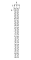
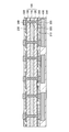
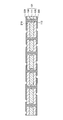
- FIG. 2 is a cross-sectional view taken along the line AA showing the laminated structure of the indirect conversion type radiation detection apparatus according to the embodiment.
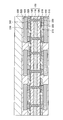
- FIG. 3 is a cross-sectional view taken along the line AA showing the laminated structure of the direct conversion type radiation detection apparatus according to the embodiment. It is the top view which showed an example of arrangement
- FIG. 2B is a cross-sectional view taken along the line AA for explaining one process of manufacturing the radiation detection apparatus shown in FIG. 2A.
- FIG. 2B is a cross-sectional view taken along the line AA for explaining one process of manufacturing the radiation detection apparatus shown in FIG. 2A.
- FIG. 2B is a cross-sectional view taken along the line AA for explaining one process of manufacturing the radiation detection apparatus shown in FIG. 2A.
- FIG. 2B is a cross-sectional view taken along the line AA for explaining one process of manufacturing the radiation detection apparatus shown in FIG. 2A.
- FIG. 2B is a cross-sectional view taken along the line AA for explaining one process of manufacturing the radiation detection apparatus shown in FIG. 2A.
- FIG. 2B is a cross-sectional view taken along the line AA for explaining one process of manufacturing the radiation detection apparatus shown in FIG. 2A.
- FIG. 2B is a cross-sectional view taken along the line AA for explaining one process of manufacturing the radiation detection apparatus shown in FIG. 2A.
- FIG. 2B is a cross-sectional view taken along the line AA for explaining one process of manufacturing the radiation detection apparatus shown in FIG. 2A.
- FIG. 2B is a cross-sectional view taken along the line AA for explaining one process of manufacturing the radiation detection apparatus shown in FIG. 2A.
- FIG. 2B is a cross-sectional view taken along the line AA for explaining one process of manufacturing the radiation detection apparatus shown in FIG. 2A.
- FIG. 2B is a cross-sectional view taken along the line AA for explaining one process of manufacturing the radiation detection apparatus shown in FIG. 2A. It is explanatory drawing which shows the element part of the radiation detection apparatus which concerns on this modification of the embodiment.
- FIG. 2B is a cross-sectional view taken along the line AA for explaining one process of manufacturing the radiation detection apparatus shown in FIG. 2A.
- FIG. 6 is a cross-sectional view taken along the line AA showing the laminated structure of the radiation detection apparatus according to the second embodiment of the present disclosure. It is the top view which showed an example of arrangement
- FIG. 16 is a cross-sectional view taken along the line AA for explaining one process for manufacturing the radiation detection apparatus shown in FIG. 15.
- FIG. 16 is a cross-sectional view taken along the line AA for explaining one process for manufacturing the radiation detection apparatus shown in FIG. 15.
- FIG. 16 is a cross-sectional view taken along the line AA for explaining one process for manufacturing the radiation detection apparatus shown in FIG. 15.
- FIG. 16 is a cross-sectional view taken along the line AA for explaining one process for manufacturing the radiation detection apparatus shown in FIG. 15.
- FIG. 16 is a cross-sectional view taken along the line AA for explaining one process for manufacturing the radiation detection apparatus shown in FIG. 15.
- FIG. 16 is a cross-sectional view taken along the line AA for explaining one process for manufacturing the radiation detection apparatus shown in FIG. 15.
- FIG. 10 is an AA cross-sectional view showing a stacked structure of a radiation detection apparatus according to a third embodiment of the present disclosure.
- FIG. 22 is a cross-sectional view taken along the line AA for explaining one process of manufacturing the radiation detection apparatus shown in FIG. 21.
- FIG. 22 is a cross-sectional view taken along the line AA for explaining one process of manufacturing the radiation detection apparatus shown in FIG. 21.
- FIG. 6 is a cross-sectional view taken along line AA showing a laminated structure of a radiation detection apparatus according to a fourth embodiment of the present disclosure.
- FIG. 25 is a cross-sectional view taken along the line AA for explaining a step of manufacturing the radiation detection apparatus shown in FIG. 24.
- FIG. 25 is a cross-sectional view taken along the line AA for explaining a step of manufacturing the radiation detection apparatus shown in FIG. 24.
- FIG. 25 is a cross-sectional view taken along the line AA for explaining a step of manufacturing the radiation detection apparatus shown in FIG. 24.
- FIG. 25 is a cross-sectional view taken along the line AA for explaining a step of manufacturing the radiation detection apparatus shown in FIG. 24. It is explanatory drawing which showed typically the radiation imaging device (or radiation imaging system) using the radiation detection apparatus which concerns on each embodiment of this indication.
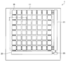
- FIG. 1 is an explanatory diagram showing the overall configuration of the radiation detection apparatus 1 according to the present embodiment.
- the radiation detection apparatus 1 according to the present embodiment detects radiation such as alpha rays, beta rays, gamma rays, and X-rays.
- the radiation detection apparatus 1 includes an element unit 11 having a plurality of radiation detection elements 10, and includes drive circuit units 21, 23, and 25 around the element unit 11.
- the element unit 11 includes a plurality of radiation detection elements 10 that generate signal charges based on incident radiation, and forms a detection region for detecting radiation.
- the plurality of radiation detection elements 10 are two-dimensionally arranged in a matrix (matrix), for example.
- the radiation detection element 10 is an element that detects radiation.
- the radiation detection element 10 may be an element that indirectly converts radiation into a signal charge (indirect conversion type), or may be an element that directly converts radiation into a signal charge (direct conversion type). .
- Examples of the element that indirectly converts radiation into signal charges include a photodiode in which a scintillator layer that emits fluorescence upon incidence of radiation is laminated on a light receiving surface.
- Examples of the radiation detection element 10 that directly converts radiation into signal charges include an element using an amorphous selenium semiconductor, a cadmium tellurium semiconductor, or the like that generates holes and electrons upon incidence of radiation. .
- the circuit element is an element constituting an electric circuit such as an IV (current-voltage) conversion circuit, an amplifier circuit, and a switch circuit.
- circuit elements are connected by signal lines (for example, ground lines, power supply lines, sample hold lines, switch selection lines, reference signal lines, reset control lines, signal output lines, etc.) wired for each row and column.
- signal lines for example, ground lines, power supply lines, sample hold lines, switch selection lines, reference signal lines, reset control lines, signal output lines, etc.
- a ground line, a power supply line, a sample hold line, and the like may be wired for each row of circuit elements, and a bias voltage for signal reading may be transmitted to the circuit elements.
- a switch selection line, a reference signal line, a reset control line, a signal output line, and the like are wired for each column of circuit elements, and an output signal read from the circuit element is transmitted to the drive circuit units 21, 23, 25, and the like. May be transmitted.
- the drive circuit units 21, 23, and 25 control driving of each circuit element in the element unit 11 and reading of signals through the signal line.
- the drive circuit units 21, 23, and 25 may read the output signal from each circuit element in the element unit 11 by driving each circuit element while scanning in units of rows or columns.
- the radiation detection apparatus 1 is a detection apparatus capable of detecting radiation in a large area, and is preferably used in a radiation imaging apparatus, a radiation imaging system, and the like.
- the radiation imaging apparatus and the radiation imaging system using the radiation detection apparatus 1 according to the present embodiment are, for example, for medical X-ray imaging apparatuses (so-called X-ray imaging apparatuses), non-destructive inspections such as baggage inspections. It can be suitably used as an X-ray imaging apparatus.
- the radiation detection apparatus 1 includes an element unit 11 having a structure in which the radiation detection elements 10 are two-dimensionally arranged in a matrix, and each radiation detection element 10 corresponds to each pixel in the imaging apparatus. It corresponds.
- the radiation detection elements 10 which are light receiving elements can be formed more densely by forming the radiation detection elements 10 more finely. Therefore, since the radiation detection apparatus 1 can reduce the element spacing of the radiation detection elements 10, it can increase the light receiving area in the element portion 11 and improve the radiation detection sensitivity. Furthermore, since the radiation detection apparatus 1 can reduce the pixels in the imaging apparatus by forming the radiation detection element 10 more finely, the resolution of the radiation imaging image can be further improved.
- the signal charge generated in the radiation detection element 10 is converted into an output signal by a circuit element arranged immediately below the radiation detection element 10.
- a radiation shielding layer (not shown) is provided between the radiation detection element 10 and the circuit element directly below. According to such a radiation shielding layer, it is possible to prevent the circuit element from being deteriorated by the radiation transmitted through the radiation detection element 10 or the like. Thereby, in the radiation detection apparatus 1, it is possible to suppress an increase in leakage current, noise, operation failure, and the like due to circuit element degradation.
- the radiation detection apparatus 1 it is also proposed to laminate a fiber optical plate (FOP) on the light receiving surface side of the radiation detection element 10 in order to shield radiation reaching the circuit element.
- FOP fiber optical plate
- the radiation incident on the radiation detection element 10 is attenuated by the FOP, so that the sensitivity of the radiation detection apparatus 1 is lowered.
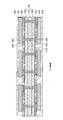
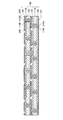
- FIG. 2A is an AA cross-sectional view showing a laminated structure of an indirect conversion type radiation detection apparatus
- FIG. 2B is an AA cross-sectional view showing a laminated structure of the direct conversion type radiation detection apparatus.
- an external wiring layer 220 is provided on one surface of the substrate 100 including the shielding insulating layer 110 sandwiched between the substrate forming layers 120 and 130, and the insulating layer 310 and the terminal electrode 330 are provided on the external wiring layer 220. Is provided.
- a circuit element 410 is provided on the terminal electrode 330, and the circuit element 410 is embedded with a protective layer 510.
- the external wiring layer 230 is provided on the other surface facing the one surface of the substrate 100, and the insulating layer 320 and the terminal electrode 340 are provided on the external wiring layer 230.
- the external wiring layer 230 is electrically connected to the external wiring layer 220 by through vias 210 penetrating the substrate forming layers 120 and 130 and the shielding insulating layer 110.
- a photoelectric conversion element 420 is provided over the terminal electrode 340, and the photoelectric conversion element 420 is embedded with a protective layer 520.
- a scintillator layer 530 and a reflective layer 540 are sequentially provided on the protective layer 520.
- the scintillator layer 530 generates fluorescence having a visible light wavelength by the incidence of radiation, and the generated fluorescence is detected by the photoelectric conversion element 420 formed below the scintillator layer 530. Thus, radiation is detected.
- the external wiring layer 220 and the external wiring layer 230 are electrically connected by a through via 210 penetrating the substrate 100.
- the radiation detection apparatus 1 can transmit the signal charge generated in the photoelectric conversion element 420 to the circuit element 410 and convert it into an output signal at a short current transmission distance, so that noise included in the output signal can be reduced. Can be reduced.
- the shielding insulating layer 110 is a layer formed of an insulator capable of shielding radiation.
- the shielding insulating layer 110 includes a metal element capable of shielding radiation and is a layer formed of an insulating material such as resin and glass.
- the shielding insulating layer 110 is preferably formed of glass having a small thermal expansion coefficient.
- the metal element capable of shielding radiation specifically represents a metal element having an atomic number of 22 or more. For example, tungsten (W), tin (Sn), lead (Pb), copper ( Cu), platinum (Pt), gold (Au), silver (Ag), nickel (Ni), strontium (Sr), barium (Ba), and the like.
- the shielding insulating layer 110 is preferably formed of lead-containing glass containing lead oxide.
- the glass containing lead contains lead oxide so that the specific gravity is 2.5 g / cm 3 or more and 5.2 g / cm 3 or less.
- the lead oxide is 20 mass% or more and 90 mass%. What is contained is preferable. Since leaded glass is inexpensive and can shield radiation with high efficiency, it can be suitably used as the shielding insulating layer 110. However, when it is difficult to use lead-containing glass due to legal restrictions or the like, for example, it is preferable to use glass containing tungsten, lead-free radiation shielding glass containing strontium, barium and the like.
- the substrate forming layers 120 and 130 are layers that sandwich the shielding insulating layer 110 and form the substrate 100.
- the substrate forming layers 120 and 130 may be formed by, for example, a prepreg in which a sheet material is impregnated with an organic resin that can be bonded to the shielding insulating layer 110.
- the substrate forming layers 120 and 130 may be formed of a prepreg in which a fibrous reinforcing material is impregnated with an epoxy or acrylic thermosetting resin.
- External wiring layers 220 and 230 are provided on the surface of the substrate 100 and electrically connect the circuit element 410 or the photoelectric conversion element 420 to other elements.
- the external wiring layers 220 and 230 can be formed of a known metal having high conductivity.
- the external wiring layers 220 and 230 may be formed of a metal such as copper (Cu), nickel (Ni), tungsten (W), platinum (Pt), gold (Au), and silver (Ag).
- the through via 210 is provided to penetrate the substrate 100 and electrically connects the external wiring layer 220 and the external wiring layer 230. Specifically, the through via 210 electrically connects a circuit element 410 and a photoelectric conversion element 420 to be described later via the external wiring layers 220 and 230 and the terminal electrodes 330 and 340. Thereby, since the through via 210 can connect the circuit element 410 and the photoelectric conversion element 420 with a short current transmission distance, noise generated when the current transmission distance becomes long can be reduced.
- the through via 210 can be formed of a known metal having high conductivity.
- the through via 210 may be formed of a metal such as copper (Cu), nickel (Ni), tungsten (W), platinum (Pt), gold (Au), and silver (Ag).
- FIG. 2A shows an example in which two through vias 210 are provided, the number of through vias 210 may be at least one and can be arbitrarily set. In FIG. The examples are not limited.
- the insulating layers 310 and 320 are provided on the external wiring layers 220 and 230, protect the external wiring layers 220 and 230, and ensure electrical insulation between the external wiring layers 220 and 230 formed on the same surface.
- the insulating layers 310 and 320 are provided with openings for forming the terminal electrodes 330 and 340 on partial regions of the external wiring layers 220 and 230.
- the insulating layers 310 and 320 can be formed of a known solder resist.
- the insulating layers 310 and 320 may be formed of an epoxy-based thermosetting resin.
- the terminal electrodes 330 and 340 are provided in the openings of the insulating layers 310 and 320, and electrically connect the external wiring layers 220 and 230 to the circuit element 410 and the photoelectric conversion element 420.
- the terminal electrodes 330 and 340 may be so-called under bump metal.
- the terminal electrodes 330 and 340 can be formed of a known metal having high conductivity.
- the terminal electrodes 330 and 340 may be formed of a metal such as nickel (Ni), platinum (Pt), gold (Au), tungsten (W), copper (Cu), and silver (Ag).
- the circuit element 410 is provided on the terminal electrode 330, is electrically connected to the photoelectric conversion element 420 through the through via 210, and converts the signal charge from the photoelectric conversion element 420 into an output signal.
- the circuit element 410 is an element constituting an electronic circuit including an IV (current-voltage) conversion circuit. With such an electric circuit, the circuit element 410 can convert the signal charge generated in the photoelectric conversion element 420 into a voltage change and output it as an output signal.
- the photoelectric conversion element 420 is provided on the terminal electrode 340, detects fluorescence generated in the scintillator layer 530 by the incidence of radiation, and generates a signal charge.
- the photoelectric conversion element 420 is preferably a photodiode, and more preferably a silicon photodiode. This is because the silicon photodiode can sufficiently absorb the light in the visible light region and can sufficiently detect the fluorescence in the visible light region generated in the scintillator layer 530.
- the silicon photodiode is more preferably one using single crystal silicon.
- a photodiode using single crystal silicon is more sensitive than a photodiode using amorphous silicon, LTPS (low temperature polycrystalline silicon), and the like, so that the detection sensitivity of the radiation detection apparatus 1 can be improved.
- a photodiode using single crystal silicon is a semiconductor that is difficult to manufacture in a large area, but in the radiation detection apparatus 1 according to the present embodiment, it is necessary to manufacture the photoelectric conversion element 420 in a large area. Is low. Therefore, a photodiode using single crystal silicon can be preferably used as the photoelectric conversion element 420.
- the protective layers 510 and 520 are provided so as to embed the circuit element 410 and the photoelectric conversion element 420 on the insulating layers 310 and 320, and protect the circuit element 410 and the photoelectric conversion element 420 from the external environment. Moreover, the intensity
- the protective layer 520 is preferably formed of a transparent resin in order to allow the fluorescence generated in the scintillator layer 530 to reach the photoelectric conversion element 420.
- the protective layer 520 in which the photoelectric conversion element 420 is embedded may be formed of a transparent resin such as an acrylic resin, an epoxy resin, polystyrene, polyvinyl chloride, or polypropylene.
- the protective layer 510 in which the circuit element 410 is embedded can be formed of a known organic resin without any particular limitation.
- the protective layer 510 may be formed of an organic resin such as an acrylic resin, an epoxy resin, polystyrene, polyvinyl chloride, polypropylene, and a polyimide resin.
- the scintillator layer 530 is provided on the protective layer 520 and emits fluorescence upon incidence of radiation. That is, the scintillator layer 530 converts the radiation incident on the light receiving surface of the radiation detection apparatus 1 into visible light or the like, and enables detection by the lower photoelectric conversion element 420.
- the scintillator layer 530 is specifically formed of a known phosphor that converts radiation such as alpha rays, beta rays, gamma rays, and X-rays into visible light.
- the scintillator layer 530 includes cesium iodide (CsI) added with thallium (Tl) or sodium (Na), sodium iodide (NaI) added with thallium (Tl), and cesium bromide added with europium (Eu).
- CsBr cesium fluoride bromide
- Eu europium
- Gd 2 O 2 S gadolinium oxysulfide
- the reflection layer 540 is formed on the scintillator layer 530, reflects the fluorescence emitted from the scintillator layer 530 to the side opposite to the photoelectric conversion element 420, and increases the fluorescence reaching the photoelectric conversion element 420.
- the reflective layer 540 is preferably formed as a metal thin film layer having a high light reflectivity.
- the reflective layer 540 is preferably formed as a thin film layer such as a silver alloy or aluminum.
- the moisture-proof layer is preferably formed using an organic film having a high water vapor barrier property such as polyparaxylylene.
- the direct conversion type radiation detection apparatus does not include the scintillator layer 530 and the reflection layer 540, but replaces the photoelectric conversion element 420 with respect to the indirect conversion type radiation detection apparatus 1 shown in FIG. 2A.
- the difference is that a radiation detecting element 421 is provided. Since the other configuration of the direct conversion type radiation detection apparatus is the same as that of the indirect conversion type radiation detection apparatus 1 shown in FIG. 2A, description thereof is omitted here.
- the radiation detection element 421 is an element that is provided on the terminal electrode 340 and generates holes and electrons by the incidence of radiation. Specifically, the radiation detection element 421 is an element that generates electrons and holes by ionizing a semiconductor in a detection region of the element by incident radiation.
- the semiconductor used for the radiation detection element 421 include an amorphous selenium semiconductor and a cadmium tellurium semiconductor.
- the scintillator layer 530 and the reflective layer 540 are not provided on the protective layer 520 in which the radiation detection element 421 is embedded. This is because the radiation detection element 421 can directly detect radiation, so that the scintillator layer 530 that converts radiation into visible light or the like, and visible light or the like generated in the scintillator layer 530 is reflected to the photoelectric conversion element 420 side. This is because it is not necessary to provide the reflective layer 540.
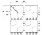
- FIG. 3 is a plan view showing an example of the arrangement relationship between the photoelectric conversion element 420 (in FIG. 2B, the radiation detection element 421) and the through via 210. As shown in FIG. 3
- the through via 210 is provided in the projection region of the photoelectric conversion element 420 in the substrate 100. Further, when a plurality of through vias 210 are provided, the through vias 210 are arranged so that the interval between them is wider. This is not preferable when the interval between the through vias 210 is narrow, because the difficulty of the process of forming the through vias 210 may increase, and the strength of the substrate 100 serving as a partition between the through vias 210 may decrease. Because.
- the arrangement of the through vias 210 is the same for each photoelectric conversion element 420, but the arrangement of the through vias 210 may be different for each photoelectric conversion element 420.
- the arrangement of the through vias 210 is different for each photoelectric conversion element 420, the interval between the through vias 210 between the adjacent photoelectric conversion elements 420 may be narrowed. Therefore, it is preferable that the arrangement of the through vias 210 is the same in each photoelectric conversion element 420.
- the interval DG between adjacent photoelectric conversion elements 420 may be, for example, 20 ⁇ m.
- the diameter VD of the through vias 210 may be 60 ⁇ m, for example, and the interval HG between the through vias 210 may be 38 ⁇ m.
- the through via 210 can be easily formed if the aspect ratio is about 2 to 3. In the above case, the through via 210 is easily formed on the substrate 100 having a thickness of about 120 ⁇ m to 180 ⁇ m. Can do.
- the radiation detection apparatus 1 uses the signal charge generated in the photoelectric conversion element 420 (radiation detection element 421 in FIG. 2B) to generate a signal with a short current transmission distance.
- the charge can be transmitted to a circuit element 410 that converts it into an output signal.
- the radiation detection apparatus 1 which concerns on this embodiment can reduce the noise contained in an output signal.
- the radiation detection apparatus 1 according to the present embodiment can suppress the deterioration of the circuit element 410 due to radiation by the shielding insulating layer 110. Thereby, the radiation detection apparatus 1 according to the present embodiment can suppress the occurrence of leakage current, noise, and malfunction due to the deteriorated circuit element 410.
- FIGS. 4 to 13 are AA cross-sectional views for explaining one process for manufacturing the radiation detection apparatus 1 shown in FIG. 2A.
- the manufacturing method shown below is an example to the last, and the manufacturing method of the radiation detection apparatus 1 which concerns on this embodiment is not necessarily limited to the following illustrations. Moreover, since it is possible to apply a well-known manufacturing apparatus and manufacturing conditions about the specific manufacturing apparatus and manufacturing conditions in each process, detailed description is abbreviate
- a laminate in which the metal foil 221, the substrate forming layer 120, the shielding insulating layer 110, the substrate forming layer 130, and the metal foil 231 are laminated is formed.
- the laminated body shown in FIG. 4 is formed by sandwiching the shielding insulating layer 110 with the substrate forming layer 120 (130) in which the metal foil 221 (231) is laminated on one side and then thermocompression bonding. Can do.
- the substrate forming layer 120 in which the metal foil 221 is laminated on one side and the shielding insulating layer 110 are bonded together to form a semi-laminate, and then the substrate forming layer 130 in which the metal foil 231 is laminated on one side
- the laminated body shown in FIG. 4 may be formed by bonding to the laminated body and thermocompression bonding.
- the shielding insulating layer 110 is, for example, a glass substrate containing a metal element, and the substrate forming layers 120 and 130 may be prepregs in which a fibrous reinforcing material is impregnated with an epoxy-based thermosetting resin.
- the metal foils 221 and 231 may be copper foils, for example.
- through holes 211 are formed in the laminate shown in FIG.
- a known method can be used. For example, drilling with a drill or a laser, wet etching using a patterned resist, or the like can be used. Note that the arrangement of the through holes 211 can be appropriately designed in consideration of the arrangement of the photoelectric conversion elements 420 and the circuit elements 410.
- the technology according to the present disclosure is not limited to the above example.
- the shielding insulating layer 110 may be formed by SOG (Spin On Glass) or the like using a mold or the like having a shape such that the shielding insulating layer 110 is not formed at a position corresponding to the through hole 211. .
- the substrate forming layers 120 and 130 and the metal foils 221 and 231 are also formed so that the respective layers are not formed at positions corresponding to the through holes 211, and the positions of the through holes 211 of the respective layers are aligned.
- a laminated body may be formed by bonding.
- the through vias 210 are formed by embedding the through holes 211 with metal.
- the through via 210 can be formed by depositing a metal such as copper on the stacked body in which the through hole 211 is formed using electroless plating using a reducing agent.
- a metal such as copper
- electroless plating using a reducing agent.
- external wiring layers 220 and 230 are formed on both surfaces of the substrate 100. Specifically, after a resist is applied onto the metal foils 221 and 231, regions where the external wiring layers 220 and 230 are formed are exposed by photolithography or the like, and the exposed resist is removed by development. Subsequently, a metal film is formed by electrolytic plating on the metal foils 221 and 231 whose metal surfaces are exposed by removing the resist, and the resist and the metal foils 221 and 231 are removed by entire surface etching. Thereby, the external wiring layers 220 and 230 are formed.
- the metal formed into the external wiring layers 220 and 230 by electrolytic plating is the same metal as the metal foils 221 and 231 in consideration of adhesion and the like, for example, copper or the like can be used.
- insulating layers 310 and 320 are formed on the external wiring layers 220 and 230 so that openings are provided in a part of regions on the external wiring layers 220 and 230.
- a solder resist for forming the insulating layers 310 and 320 is applied on the external wiring layers 220 and 230.
- the exposed solder resist is removed by development, whereby the external wiring layers 220 and 230 are formed on the insulating layers 310 and 320. An opening that exposes a portion of is formed.
- a region where the opening is formed is preferably a region including a region directly below the through via 210 in order to shorten a current transmission distance between the photoelectric conversion element 420 and the circuit element 410.
- terminal electrodes 330 and 340 are formed in the openings of the insulating layers 310 and 320. Specifically, the terminal electrodes 330 and 340 are formed in the openings of the insulating layers 310 and 320 by electrolytic plating or substitutional electroless plating. The terminal electrodes 330 and 340 function as terminals of the external wiring layers 220 and 230.
- the terminal electrodes 330 and 340 can be formed of a metal such as nickel (Ni), platinum (Pt), and gold (Au), for example, in order to suppress wiring resistance.
- electrolytic plating in order to plate the terminal electrodes 330 and 340 only on the openings.
- noble metals Pt, Au, etc.
- substitutional electroless plating in which plating is performed only on the metal surface.
- the circuit element 410 is mounted on the terminal electrode 330, and the protective layer 510 is formed on the insulating layer 310 so as to embed the circuit element 410.
- solder or the like is applied onto the terminal electrode 330, and the terminal electrode 330 and a terminal (pad) of an IC (Integrated Circuit) element including an IV conversion circuit are aligned and thermocompression bonded, whereby the terminal A circuit element 410 is mounted on the electrode 330.
- the protective layer 510 is formed by applying an organic resin or the like over the insulating layer 310.
- any organic resin can be used as long as it is used as an embedding material or a sealing material such as an IC chip.
- the photoelectric conversion element 420 is mounted on the terminal electrode 340, and the protective layer 520 is formed on the insulating layer 320 so as to embed the photoelectric conversion element 420.
- solder or the like is applied onto the terminal electrode 340, and the position of the terminal electrode 340 and the terminal (pad) of the photoelectric conversion element 420 such as a photodiode are aligned and thermocompression bonded, whereby the terminal electrode 340 A photoelectric conversion element 420 is mounted.
- the protective layer 520 is formed by applying an organic resin or the like over the insulating layer 320.
- the protective layer 520 can be any organic resin as long as it is used as an embedding material or sealing material such as an IC chip and is transparent.
- a scintillator layer 530 is formed on the protective layer 520.
- the scintillator layer 530 can be formed by vaporizing a compound that forms the scintillator layer 530 in a vacuum apparatus and vapor-depositing it on the protective layer 520 using a vapor deposition method or the like.
- a known phosphor as described above can be used as the compound that forms the scintillator layer 530.
- a reflective layer 540 is formed on the scintillator layer 530.
- the reflective layer 540 can be formed by vapor-depositing a silver alloy, aluminum, or the like using a vacuum vapor deposition method such as a PVD (Physical Vapor Deposition) method or a sputtering method.
- a vacuum vapor deposition method such as a PVD (Physical Vapor Deposition) method or a sputtering method.
- the radiation detection apparatus 1 can be manufactured through the above steps.
- the radiation detection apparatus 1 manufactured by such a process reduces noise included in the output signal because the photoelectric conversion element 420 and the circuit element 410 are connected by the through via 210 at a short current transmission distance. It is possible.
- the radiation detection apparatus 1 since the radiation detection apparatus 1 includes the shielding insulating layer 110 between the photoelectric conversion element 420 and the circuit element 410, the radiation detection apparatus 1 suppresses deterioration of the circuit element 410 due to radiation, and leak current caused by the deteriorated circuit element 410. The occurrence of noise and malfunction can be suppressed.
- FIG. 14 is an explanatory diagram showing an element part of the radiation detection apparatus according to this modification.
- the element part 11A of the radiation detection apparatus according to this modification for example, two radiation detection elements 10A are formed as one set.
- One circuit element (not shown) including an IV conversion circuit and the like is provided for one set of radiation detection elements 10A. That is, the radiation detection apparatus according to this modification is different in that one circuit element is provided for the plurality of radiation detection elements 10A.
- a circuit element provided directly below the plurality of radiation detection elements 10A is connected to the plurality of radiation detection elements 10A in order to convert signal charges generated in each of the radiation detection elements 10A into output signals.
- FIG. 14 shows an example in which one circuit element is provided directly below the two radiation detection elements 10A, but the present modification is not limited to the above example. In this modification, it is sufficient that one circuit element is provided for at least two or more radiation detection elements 10A. For example, one circuit element is provided for four radiation detection elements 10A. May be.
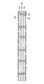
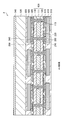
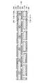
- FIG. 15 is a cross-sectional view taken along line AA showing the laminated structure of the radiation detection apparatus according to the present embodiment.
- an indirect conversion type radiation detection apparatus will be mainly described as an example, but it goes without saying that the radiation detection apparatus according to the present embodiment may be a direct conversion type radiation detection apparatus.
- an external wiring layer 220 is provided on one surface of the substrate 101 including the shielding metal layer 111 sandwiched between the substrate forming layers 120 and 130, and the insulating layer 310 and the terminal electrode 330 are provided on the external wiring layer 220. Is provided.
- a circuit element 410 is provided on the terminal electrode 330, and the circuit element 410 is embedded with a protective layer 510.
- the external wiring layer 230 is provided on the other surface facing the one surface of the substrate 101, and the insulating layer 320 and the terminal electrode 340 are provided on the external wiring layer 230.
- the external wiring layer 230 is electrically connected to the external wiring layer 220 through a through via 210 that passes through the substrate forming layers 120 and 130 and passes through the opening 113 of the shielding metal layer 111.
- a photoelectric conversion element 420 is provided over the terminal electrode 340, and the photoelectric conversion element 420 is embedded with a protective layer 520.
- a scintillator layer 530 and a reflective layer 540 are sequentially provided on the protective layer 520.
- the radiation detection apparatus 2 according to the second embodiment is different from the radiation detection apparatus 1 according to the first embodiment in that the substrate 101 includes a shielding metal layer 111 instead of the shielding insulating layer 110.
- the external wiring layer 220 and the external wiring layer 230 are electrically connected by a through via 210 formed through the opening 113 provided in the shielding metal layer 111.
- the through via 210 is formed through the opening 113 provided in the shielding metal layer 111 so as not to contact the shielding metal layer 111.
- the radiation detection apparatus 2 can transmit the signal charge generated in the photoelectric conversion element 420 to the circuit element 410 at a short current transmission distance and convert it to the output signal, thereby reducing noise included in the output signal. can do.
- the radiation detection apparatus 2 can be electrically insulated from the through via 210 and the shielding metal layer 111, occurrence of a short circuit (short circuit) can be suppressed.
- At least one of the external wiring layers 220 and 230 and the terminal electrodes 330 and 340 is a region that secures electrical insulation between the through via 210 and the shielding metal layer 111 (hereinafter, an insulation securing region). (Also referred to as).
- the shielding metal layer 111 is a layer formed of a metal capable of shielding radiation.
- the metal capable of shielding radiation specifically represents a metal element having an atomic number of 22 or more, for example, tungsten (W), iron (Fe), lead (Pb), gold (Au), It represents platinum (Pt), silver (Ag), copper (Cu), chromium (Cr), nickel (Ni), molybdenum (Mo), tin (Sn), and the like.
- metals capable of shielding radiation include tungsten (W), lead (Pb), copper (Cu), chromium (Cr), nickel (Ni), gold (Au), platinum (Pt), silver (Ag) and tin (Sn) are preferred.
- an opening 113 is formed in the shielding metal layer 111 so as to allow the through via 210 to pass therethrough. Since the shielding metal layer 111 has conductivity, when the shielding metal layer 111 and the through via 210 are in contact with each other, a short circuit may occur. Therefore, in the present embodiment, the opening 113 having a diameter larger than the diameter of the through via 210 is formed in the shielding metal layer 111, and the through via 210 is formed so as to pass through the opening 113, thereby generating a short circuit. Is preventing.
- the through via 210 and the shielding metal layer 111 may be in contact with each other. Not too long.
- At least one of the external wiring layers 220 and 230 and the terminal electrodes 330 and 340 is a region that secures electrical insulation between the through via 210 and the shielding metal layer 111 (hereinafter referred to as “a region”). Then, it is also formed in a region corresponding to an insulation securing region). This is because, in the insulation securing region between the through via 210 and the shielding metal layer 111, neither the through via 210 nor the shielding metal layer 111 is formed, so that radiation is not shielded by the through via 210 and the shielding metal layer 111. is there.
- the radiation detection apparatus 2 forms at least one of the external wiring layers 220 and 230 made of metal and the terminal electrodes 330 and 340 in a region corresponding to the insulation ensuring region, so that the radiation in the insulation ensuring region is formed. Shielding is possible. Thereby, the radiation detection apparatus 2 can suppress deterioration of the circuit element 410 due to radiation. Further, in order to shield radiation more reliably, it is preferable that more metal layers (external wiring layers 220 and 230 and terminal electrodes 330 and 340) are formed in a region corresponding to the insulation ensuring region.
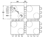
- FIG. 16 is a plan view illustrating an example of an arrangement relationship between the photoelectric conversion element and the through via.
- the opening 113 is provided in the projection region of the photoelectric conversion element 420 in the substrate 101. Further, the through via 210 passes through the opening 113.
- a region where the through via passes in the opening 113 is the through via region 213, and an outer peripheral region of the through via region 213 in the opening 113 is the insulation securing region 115.
- the openings 113 are arranged so that the interval between them becomes wider. This is not preferable when the distance between the openings 113 is narrow, because the difficulty of the process of forming the openings 113 may increase and the strength of the substrate 101 serving as a partition between the openings 113 may decrease. Because.
- the arrangement of the through via 210 and the opening 113 is the same for each photoelectric conversion element 420, but the arrangement of the through via 210 and the opening 113 may be different for each photoelectric conversion element 420. .
- the arrangement of the opening 113 is different for each photoelectric conversion element 420, there is a possibility that the interval between the openings 113 is narrowed between the adjacent photoelectric conversion elements 420. Therefore, it is preferable that the arrangement of the through via 210 and the opening 113 is the same in each photoelectric conversion element 420.
- the interval DG between adjacent photoelectric conversion elements 420 may be, for example, 20 ⁇ m.
- the diameter HD of the opening 113 may be 60 ⁇ m, for example, and the diameter VD of the through via region 213 may be 40 ⁇ m.
- the width of the insulation ensuring region 115 is preferably 10 ⁇ m. This is because in order to ensure the insulation between the through via 210 and the shielding metal layer 111, it is preferable that an insulator of at least 10 ⁇ m or more exists between them. Further, the interval HG between the openings 113 may be 38 ⁇ m. Since the through via 210 can be easily formed if the aspect ratio is about 2 to 3, in the above case, the through via 210 is easily formed on the substrate 101 having a thickness of about 80 ⁇ m to 120 ⁇ m. Can do.
- the radiation detection apparatus 2 converts the signal charge generated by the photoelectric conversion element 420 into an output signal at a short current transmission distance. Can be transmitted. Thereby, the radiation detection apparatus 2 which concerns on this embodiment can reduce the noise contained in an output signal.
- the radiation detection apparatus 2 can shield radiation reaching the circuit element 410 by the shielding metal layer 111, the through via 210, the external wiring layers 220 and 230, and the terminal electrodes 330 and 340. Therefore, the radiation detection apparatus 2 can suppress the deterioration of the circuit element 410 due to the radiation, and can suppress the occurrence of leakage current, noise, and malfunction due to the deteriorated circuit element 410.
- FIGS. 17 to 20 are cross-sectional views taken along the line AA for explaining one process for manufacturing the radiation detection apparatus 2 shown in FIG.
- FIGS. 17 to 20 are cross-sectional views taken along the line AA for explaining one process for manufacturing the radiation detection apparatus 2 shown in FIG.
- the manufacturing method shown below is an example to the last, and the manufacturing method of the radiation detection apparatus 2 which concerns on this embodiment is not necessarily limited to the following illustrations. Moreover, since it is possible to apply a well-known manufacturing apparatus and manufacturing conditions about the specific manufacturing apparatus and manufacturing conditions in each process, detailed description is abbreviate
- a laminated body is formed in which the metal foil 221, the substrate forming layer 120, the shielding metal layer 111 in which the opening 113 is formed, the substrate forming layers 120 and 130, and the metal foil 221 are laminated.
- the laminate shown in FIG. 17 is formed by sandwiching the shielding metal layer 111 with the substrate forming layer 120 (130) having the metal foil 221 (231) laminated on one side and then thermocompression bonding. Can do.
- the substrate forming layer 120 having the metal foil 221 laminated on one side and the shielding metal layer 111 are bonded together to form a semi-laminated body, and then the substrate forming layer 130 having the metal foil 231 laminated on one side is formed into the half laminated body.
- the laminated body shown in FIG. 17 may be formed by bonding to the laminated body and thermocompression bonding.
- the substrate forming layers 120 and 130 may be prepregs in which a fibrous reinforcing material is impregnated with an epoxy thermosetting resin, and the metal foils 221 and 231 may be copper foils, for example.
- the shielding metal layer 111 is a metal layer made of, for example, tungsten and has an opening 113.
- the opening 113 is formed in an arrangement corresponding to the arrangement of the through via 210 to be formed. Further, in order to ensure electrical insulation between the shielding metal layer 111 and the through via 210, the opening 113 is formed with a diameter larger than the diameter of the through via 210.
- through holes 211 are formed in the laminate shown in FIG.
- a known method can be used. For example, drilling with a drill or a laser, wet etching using a patterned resist, or the like can be used.
- the through hole 211 in which the through via 210 is formed is formed in the opening 113 in order to ensure electrical insulation between the shielding metal layer 111 and the through via 210.
- the through hole 211 is filled with metal to form a through via 210.
- the through via 210 can be formed by depositing a metal such as copper on the stacked body in which the through hole 211 is formed using electroless plating using a reducing agent.
- a metal such as copper
- electroless plating using a reducing agent.
- external wiring layers 220 and 230 are formed on both surfaces of the substrate 101. Specifically, after a resist is applied onto the metal foils 221 and 231, regions where the external wiring layers 220 and 230 are formed are exposed by photolithography or the like, and the exposed resist is removed by development. Subsequently, a metal film is formed by electrolytic plating on the metal foils 221 and 231 whose metal surfaces are exposed by removing the resist, and the resist and the metal foils 221 and 231 are removed by entire surface etching. Thereby, the external wiring layers 220 and 230 are formed.
- the metal formed as the external wiring layers 220 and 230 by electrolytic plating is preferably the same metal as the metal foils 221 and 231 in view of adhesion and the like, for example, copper is preferably used.
- the radiation detection apparatus 2 can be manufactured through the above steps.
- the radiation detection apparatus 2 manufactured by such a process reduces noise included in the output signal because the photoelectric conversion element 420 and the circuit element 410 are connected by the through via 210 at a short current transmission distance. It is possible.
- the radiation detection apparatus 2 can shield the radiation reaching the circuit element 410 by the shielding metal layer 111, the through via 210, the external wiring layers 220 and 230, and the terminal electrodes 330 and 340, the radiation of the circuit element 410 Deterioration can be suppressed. Thereby, the radiation detection apparatus 2 according to the present embodiment can suppress the occurrence of leakage current, noise, and malfunction due to the deteriorated circuit element 410.
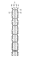
- FIG. 21 is a cross-sectional view along the line AA showing the laminated structure of the radiation detection apparatus 3 according to this embodiment.
- an indirect conversion type radiation detection apparatus will be mainly described as an example, but it goes without saying that the radiation detection apparatus according to the present embodiment may be a direct conversion type radiation detection apparatus.
- the substrate 103 includes a shielding insulating layer 110 and a shielding metal layer 111.
- a substrate formation layer 130 is provided between the shielding insulating layer 110 and the shielding metal layer 111, and the substrate 103 is formed by stacking the shielding insulating layer 110, the substrate forming layer 130, and the shielding metal layer 111. It is formed by being sandwiched between layers 120 and 140.
- an external wiring layer 220 is provided on one surface of the substrate 103, and an insulating layer 310 and a terminal electrode 330 are provided on the external wiring layer 220.
- a circuit element 410 is provided on the terminal electrode 330, and the circuit element 410 is embedded with a protective layer 510.
- an external wiring layer 230 is provided on the other surface facing one surface of the substrate 103, and an insulating layer 320 and a terminal electrode 340 are provided on the external wiring layer 230.
- the external wiring layer 230 is electrically connected to the external wiring layer 220 by a through via 210 that penetrates the shielding insulating layer 110, the shielding metal layer 111, and the substrate forming layers 120, 130, and 140.
- a photoelectric conversion element 420 is provided over the terminal electrode 340, and the photoelectric conversion element 420 is embedded with a protective layer 520.
- a scintillator layer 530 and a reflective layer 540 are sequentially provided on the protective layer 520.
- the radiation detection apparatus 3 according to the third embodiment is different from the radiation detection apparatus 1 according to the first embodiment in that the substrate 103 includes the shielding insulating layer 110 and the shielding metal layer 111.
- the radiation detection apparatus 3 according to the present embodiment for example, when the shielding insulation layer 110 alone is not enough to shield radiation, or when it is difficult to form the shielding insulation layer 110 and the shielding metal layer 111 thick. In addition, radiation can be shielded more reliably.
- the external wiring layer 220 and the external wiring layer 230 are electrically connected by a through via 210 penetrating the substrate 103.
- the through via 210 is formed through the opening 113 provided in the shielding metal layer 111 so as not to contact the shielding metal layer 111.
- the radiation detection apparatus 3 can transmit the signal charge generated in the photoelectric conversion element 420 to the circuit element 410 at a short current transmission distance and convert it to the output signal, thereby reducing noise included in the output signal. can do.
- the radiation detection apparatus 3 can electrically insulate the through via 210 and the shielding metal layer 111, the occurrence of a short circuit (short circuit) can be suppressed.
- the radiation detection apparatus 3 is configured to receive radiation that reaches the circuit element 410 by at least one of the external wiring layers 220 and 230 and the terminal electrodes 330 and 340 even in the insulation ensuring region where the shielding metal layer 111 is not formed. Can be shielded.
- metal layers (external wiring layers 220 and 230 and terminal electrodes 330 and 340) are formed in a region corresponding to the insulation ensuring region.
- 21 illustrates an example in which the shielding insulating layer 110 is formed on the circuit element 410 side and the shielding metal layer 111 is formed on the photoelectric conversion element 420 side, but the technology according to the present disclosure is limited to the above examples. Not.
- the shielding metal layer 111 may be formed on the circuit element 410 side, and the shielding insulating layer 110 may be formed on the photoelectric conversion element 420 side.
- the manufacturing method shown below is an example to the last, and the manufacturing method of the radiation detection apparatus 2 which concerns on this embodiment is not necessarily limited to the following illustrations. Moreover, since it is possible to apply a well-known manufacturing apparatus and manufacturing conditions about the specific manufacturing apparatus and manufacturing conditions in each process, detailed description is abbreviate
- a laminate in which the metal foil 221, the substrate forming layer 120, the shielding insulating layer 110, the substrate forming layer 130, the shielding metal layer 111, the substrate forming layer 140, and the metal foil 231 are laminated is formed.
- the shielding metal layer 111 in which the opening 113 is formed and the shielding insulating layer 110 are bonded through the substrate forming layer 120.
- the laminate in which the shielding metal layer 111, the substrate forming layer 120, and the shielding insulating layer 110 are bonded is sandwiched between the substrate forming layer 120 (140) in which the metal foil 221 (231) is laminated on one side,
- the stacked body shown in FIG. 21 can be formed by pressure bonding.
- the shielding insulating layer 110 is, for example, a glass substrate containing a metal element.
- the shielding metal layer 111 is a metal layer made of, for example, tungsten and having an opening 113 formed in an arrangement corresponding to the arrangement of the through via 210.
- the opening 113 is formed with a diameter larger than the diameter of the through via 210.
- the substrate forming layers 120, 130, and 140 may be prepregs in which a fibrous reinforcing material is impregnated with an epoxy-based thermosetting resin.
- the metal foils 221 and 231 may be copper foils, for example.
- through holes 211 are formed in the laminate shown in FIG.
- a known method can be used. For example, drilling or laser drilling, wet etching using a patterned resist, or the like can be used.
- the through hole 211 in which the through via 210 is formed is formed in the opening 113 in order to ensure electrical insulation between the shielding metal layer 111 and the through via 210.
- the radiation detection apparatus 3 can be manufactured through the above steps.
- the radiation detection device 3 manufactured by such a process reduces noise included in the output signal because the photoelectric conversion element 420 and the circuit element 410 are connected by the through via 210 at a short current transmission distance. Is possible.
- the radiation detection device 3 can more reliably shield the radiation reaching the circuit element 410 by the shielding insulating layer 110 and the shielding metal layer 111. Thereby, the radiation detection apparatus 3 can further suppress the occurrence of leakage current, noise, and malfunction due to deterioration of the circuit element 410 due to radiation.
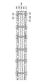
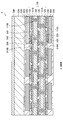
- FIG. 24 is a cross-sectional view taken along line AA showing the laminated structure of the radiation detection apparatus 4 according to this embodiment.
- an indirect conversion type radiation detection apparatus will be mainly described as an example, but it goes without saying that the radiation detection apparatus according to the present embodiment may be a direct conversion type radiation detection apparatus.
- the substrate 105 includes a first shielding metal layer 111A and a second shielding metal layer 111B. Further, a substrate forming layer 130, an internal wiring layer 240, and a substrate forming layer 140 are provided between the first shielding metal layer 111A and the second shielding metal layer 111B to form a laminate. . In addition, the substrate 105 is formed by further sandwiching the stacked body between substrate forming layers 120 and 150.
- an external wiring layer 220 is provided on one surface of the substrate 103, and an insulating layer 310 and a terminal electrode 330 are provided on the external wiring layer 220.
- a circuit element 410 is provided on the terminal electrode 330, and the circuit element 410 is embedded with a protective layer 510.
- an external wiring layer 230 is provided on the other surface facing one surface of the substrate 103, and an insulating layer 320 and a terminal electrode 340 are provided on the external wiring layer 230.
- the external wiring layer 230 is electrically connected to the internal wiring layer 240 by a second through via 210B that penetrates the second shielding metal layer 111B and the substrate forming layers 150 and 140.
- the external wiring layer 220 is electrically connected to the first shielding metal layer 111A and the first through vias 210A penetrating the substrate forming layers 130 and 120.
- a photoelectric conversion element 420 is provided over the terminal electrode 340, and the photoelectric conversion element 420 is embedded with a protective layer 520.
- a scintillator layer 530 and a reflective layer 540 are sequentially provided on the protective layer 520.
- the first embodiment is that the substrate 105 includes a plurality of shielding metal layers (first shielding metal layer 111A and second shielding metal layer 111B). It differs from the radiation detection apparatus 1 which concerns on a form. According to the radiation detection apparatus 4 according to the present embodiment, for example, when it is difficult to form a thick shielding metal layer, radiation can be shielded more reliably.
- the external wiring layer 220 and the external wiring layer 230 are electrically connected by the first through via 210A, the second through via 210B, and the internal wiring layer 240.
- the first through via 210A is formed through the first opening 113A provided in the first shielding metal layer 111A so as not to contact the first shielding metal layer 111A.
- the second through via 210B is formed through the second opening 113B provided in the second shielding metal layer 111B so as not to contact the second shielding metal layer 111B.
- the radiation detection apparatus 4 can transmit the signal charge generated in the photoelectric conversion element 420 to the circuit element 410 at a short current transmission distance and convert it to the output signal, thereby reducing noise included in the output signal. can do. Further, the radiation detection device 4 electrically insulates between the first through via 210A and the first shielding metal layer 111A and between the second through via 210B and the second shielding metal layer 111B. Therefore, the occurrence of a short circuit (short circuit) can be suppressed.
- At least one of the external wiring layers 220 and 230, the internal wiring layer 240, and the terminal electrodes 330 and 340 includes the first shielding metal layer 111A and the second shielding metal layer 111A.
- the shielding metal layer 111B is formed in a region corresponding to the insulation ensuring region.
- the radiation detection apparatus 4 is configured so that the external wiring layers 220 and 230, the internal wiring layer 240, and the terminal electrode are provided in the insulation ensuring region where the first shielding metal layer 111A and the second shielding metal layer 111B are not formed.
- the radiation reaching the circuit element 410 can be shielded by at least one of 330 and 340.
- metal layers In order to shield radiation more reliably, more metal layers (external wiring layers 220 and 230, internal wiring layers 240, and terminal electrodes 330 and 340) are formed in a region corresponding to the insulation ensuring region. It is preferable.
- the region where the first opening 113A is formed and the region where the second opening 113B is formed do not overlap when viewed from one surface side of the substrate 105 in plan view. This is because the regions where the first shielding metal layer 111A and the second shielding metal layer 111B having a high radiation shielding effect are not overlapped with each other cause a large difference in the radiation shielding effect depending on the region. This is to prevent it from occurring.
- FIGS. 25 to 28 are AA cross-sectional views for explaining one process for manufacturing the radiation detection apparatus 4 shown in FIG.
- FIGS. 25 to 28 are AA cross-sectional views for explaining one process for manufacturing the radiation detection apparatus 4 shown in FIG.
- FIGS. 25 to 28 are AA cross-sectional views for explaining one process for manufacturing the radiation detection apparatus 4 shown in FIG.
- FIGS. 25 to 28 are AA cross-sectional views for explaining one process for manufacturing the radiation detection apparatus 4 shown in FIG.
- FIGS. 25 to 28 are AA cross-sectional views for explaining one process for manufacturing the radiation detection apparatus 4 shown in FIG.
- only characteristic processes will be described, and description of processes substantially similar to the processes described in the first and second embodiments will be omitted.
- the manufacturing method shown below is an example to the last, and the manufacturing method of the radiation detection apparatus 2 which concerns on this embodiment is not necessarily limited to the following illustrations. Moreover, since it is possible to apply a well-known manufacturing apparatus and manufacturing conditions about the specific manufacturing apparatus and manufacturing conditions in each process, detailed description is abbreviate
- the substrate forming layer 130 As shown in FIG. 25, for example, by stacking the substrate forming layer 130, the first shielding metal layer 111A, the substrate forming layer 120, and the metal foil 221 on the stacked body shown in FIG. Is formed.
- the first shielding metal layer 111A in which the first opening 113A is formed is bonded to one surface of the stacked body shown in FIG.
- the substrate forming layer 120 having the metal foil 221 laminated on one side is bonded to the first shielding metal layer 111A and thermocompression bonded, whereby the laminate shown in FIG. 25 can be formed.
- the first shielding metal layer 111A is a metal layer made of, for example, tungsten and having the first opening 113A.
- the first opening 113A is preferably formed in any region where the internal wiring layer 240 is formed, and is not formed in a region immediately below the second opening 113B.
- the substrate forming layers 120 and 130 may be prepregs in which a fibrous reinforcing material is impregnated with an epoxy thermosetting resin.
- the metal foil 221 may be a copper foil, for example.
- the first through-hole 211A is formed in the laminate shown in FIG.
- the first through hole 211A is formed so as to expose the internal wiring layer 240.
- a known method can be used. For example, drilling or laser drilling, wet etching using a patterned resist, or the like can be used.
- first through hole 211A in which the first through via 210A is formed is provided in the first through hole 211A in order to ensure electrical insulation between the first shielding metal layer 111A and the first through via 210A. Is formed in the opening 113A.
- the first through-hole 211A is filled with metal to form a first through-via 210A.
- the first through via 210A is formed by depositing a metal such as copper on the stacked body in which the first through hole 211A is formed by using electroless plating using a reducing agent. Can be formed.
- the first through via 210A is electrically connected to the internal wiring layer 240.
- a reduction type electroless plating using a reducing agent.
- an external wiring layer 220 is formed on the metal foil 221 side of the substrate 105. Specifically, after applying a resist on the metal foil 221, a region for forming the external wiring layer 220 is exposed by photolithography or the like, and the exposed resist is removed by development. Subsequently, a metal film is formed by electrolytic plating on the metal foils 221 and 231 whose metal surfaces are exposed by removing the resist, and the resist and the metal foil 221 are removed by whole surface etching. Thereby, the external wiring layer 220 is formed.
- the metal formed as the external wiring layer 220 by electrolytic plating is the same metal as the metal foil 221 in view of adhesion and the like, for example, copper is preferably used.
- the radiation detection apparatus 4 can be manufactured through the above steps.
- the photoelectric conversion element 420 and the circuit element 410 are arranged at a short current transmission distance by the first through via 210A, the internal wiring layer 240, and the second through via 210B. Since it is connected, it is possible to reduce noise included in the output signal.
- the radiation detection device 4 can shield the radiation reaching the circuit element 410 with a plurality of shielding metal layers (first shielding metal layer 111A and second shielding metal layer 111B). Deterioration can be further suppressed. Thereby, the radiation detection apparatus 4 according to the present embodiment can suppress the occurrence of leakage current, noise, and malfunction caused by the deteriorated circuit element 410.
- the radiation detection apparatus 4 showed the structure which has two shielding metal layers in the above, the technique which concerns on this indication is not limited above.
- the radiation detection apparatus 4 may have three or more shielding metal layers. Any one of the shielding metal layers may be replaced with a shielding insulating layer.
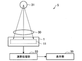
- FIG. 29 is an explanatory diagram schematically illustrating a radiation imaging apparatus (or radiation imaging system) using the radiation detection apparatus according to each embodiment of the present disclosure.
- the radiation detection apparatus according to each embodiment of the present disclosure is applicable to, for example, the radiation imaging apparatus (or radiation imaging system) illustrated in FIG.
- the radiation imaging apparatus 5 includes the radiation detection apparatus 1 according to each embodiment, an arithmetic processing unit 33, and a display unit 35.
- the calculation processing unit 33 generates a captured image by performing calculation processing on the detection signal output from the radiation detection apparatus 1.
- the display unit 35 displays a display image based on the captured image generated by the arithmetic processing unit 33.
- a radiation imaging apparatus 5 In such a radiation imaging apparatus 5, first, radiation is emitted from a light source (for example, a radiation source such as an X-ray source) 31 toward the subject 30, and the radiation transmitted through the subject 30 is an element unit in the radiation detection apparatus 1. 11 is detected. Next, the radiation detection device 1 outputs an output signal from the element unit 11 to the arithmetic processing unit 33, and the arithmetic processing unit 33 performs arithmetic processing on the output signal from the radiation detection device 1 to generate a captured image. The captured image signal is output to the display unit 35. The display unit 35 displays the captured image captured by the radiation imaging apparatus 5 as a display image based on the captured image signal from the arithmetic processing unit 33.
- a light source for example, a radiation source such as an X-ray source
- the radiation imaging apparatus 5 (or radiation imaging system) according to this application example can acquire a radiation imaging image of the subject 30 based on the output signal from the radiation detection apparatus 1. It is. In addition, the radiation imaging apparatus 5 according to this application example can also display the radiation imaging image of the subject 30 by outputting the acquired imaging signal based on the radiation to the display unit 35 or an external display device.
- a substrate including a radiation shielding layer; A plurality of radiation detection elements arranged two-dimensionally on one surface of the substrate; A circuit element disposed on the other surface of the substrate facing the surface on which the radiation detection elements are arranged, and electrically connected to at least one of the radiation detection elements by a through via penetrating the substrate;
- a radiation detection apparatus comprising: (2) The radiation detection apparatus according to (1), wherein the radiation shielding layer is an insulating layer containing a metal element. (3) The radiation detection apparatus according to (2), wherein the radiation shielding layer is formed of glass containing a metal element. (4) The radiation detection apparatus according to (1), wherein the radiation shielding layer is a metal layer.
- the substrate includes a plurality of the radiation shielding layers, The radiation detection apparatus according to (5) or (6), wherein the through via passes through each of the radiation shielding layers at an opening formed in a different planar region of the radiation shielding layer.
- the radiation detection apparatus according to any one of (1) to (6), wherein the substrate includes a single radiation shielding layer.
- the electric circuit including the circuit element includes a current-voltage conversion circuit.
- the radiation detection element is an element that directly converts radiation into an electrical signal.
- the circuit element is electrically connected to a plurality of the radiation detection elements.
- a substrate including a radiation shielding layer, a plurality of radiation detection elements two-dimensionally arranged on one surface of the substrate, and a surface of the substrate opposite to the surface on which the radiation detection elements are arranged are disposed and penetrates the substrate
- a radiation detection device comprising: a circuit element electrically connected to at least one of the radiation detection elements by a through via; An arithmetic processing unit that arithmetically processes an output signal from the radiation detection device and generates a captured image;
- An imaging apparatus having (13) A substrate including a radiation shielding layer, a plurality of radiation detection elements two-dimensionally arranged on one surface of the substrate, and a surface of the substrate opposite to the surface on which the radiation detection elements are arranged are disposed and penetrates the substrate
- a radiation detection device comprising: a circuit element electrically connected to at least one of the radiation detection elements by a through via; An arithmetic processing unit that arithmetically processes an output signal from the radiation detection device and generates a captured image;
- Radiation detection apparatus 1
- Radiation imaging apparatus 10
- Radiation detection element 11 Element part 110 Shielding insulating layer 111 Shielding metal layer 113 Opening part 120, 130, 140, 150
- Substrate formation layer 210 Through-via 220, 230 External wiring Layer 240 Internal wiring layer 310, 320 Insulating layer 330, 340 Terminal electrode 410 Circuit element 420 Photoelectric conversion element 510, 520 Protective layer 530 Scintillator layer 540 Reflective layer
Landscapes
- Health & Medical Sciences (AREA)
- Life Sciences & Earth Sciences (AREA)
- Physics & Mathematics (AREA)
- Engineering & Computer Science (AREA)
- Molecular Biology (AREA)
- High Energy & Nuclear Physics (AREA)
- Medical Informatics (AREA)
- Radiology & Medical Imaging (AREA)
- Surgery (AREA)
- Pathology (AREA)
- Nuclear Medicine, Radiotherapy & Molecular Imaging (AREA)
- Biomedical Technology (AREA)
- Heart & Thoracic Surgery (AREA)
- Biophysics (AREA)
- Optics & Photonics (AREA)
- Animal Behavior & Ethology (AREA)
- General Health & Medical Sciences (AREA)
- Public Health (AREA)
- Veterinary Medicine (AREA)
- General Physics & Mathematics (AREA)
- Spectroscopy & Molecular Physics (AREA)
- Measurement Of Radiation (AREA)
- Apparatus For Radiation Diagnosis (AREA)
Abstract
L'invention cherche à permettre la détection de doses inférieures de rayonnement. Pour ce faire, l'invention prévoit un dispositif de détection de rayonnement qui comporte un substrat comprenant une couche de protection contre le rayonnement, une pluralité d'éléments de détection de rayonnement disposés de façon bidimensionnelle sur une surface du substrat, et un élément de circuit qui est disposé sur l'autre surface du substrat, opposée à la surface sur laquelle les éléments de détection de rayonnement sont disposés, et qui est connecté électriquement à un ou plusieurs des éléments de détection de rayonnement par un trou d'interconnexion traversant qui pénètre dans le substrat.
Applications Claiming Priority (2)
| Application Number | Priority Date | Filing Date | Title |
|---|---|---|---|
| JP2015-090393 | 2015-04-27 | ||
| JP2015090393A JP2016206101A (ja) | 2015-04-27 | 2015-04-27 | 放射線検出装置、撮像装置、および撮像システム |
Publications (1)
| Publication Number | Publication Date |
|---|---|
| WO2016174939A1 true WO2016174939A1 (fr) | 2016-11-03 |
Family
ID=57199672
Family Applications (1)
| Application Number | Title | Priority Date | Filing Date |
|---|---|---|---|
| PCT/JP2016/057474 Ceased WO2016174939A1 (fr) | 2015-04-27 | 2016-03-09 | Dispositif de détection de rayonnement, dispositif d'imagerie et système d'imagerie |
Country Status (2)
| Country | Link |
|---|---|
| JP (1) | JP2016206101A (fr) |
| WO (1) | WO2016174939A1 (fr) |
Families Citing this family (1)
| Publication number | Priority date | Publication date | Assignee | Title |
|---|---|---|---|---|
| JP7534253B2 (ja) * | 2021-03-26 | 2024-08-14 | 京セラ株式会社 | 基板、検出装置および検出モジュール |
Citations (4)
| Publication number | Priority date | Publication date | Assignee | Title |
|---|---|---|---|---|
| JP2004209117A (ja) * | 2003-01-08 | 2004-07-29 | Hitachi Medical Corp | 放射線検出装置およびその製造方法 |
| JP2004219318A (ja) * | 2003-01-16 | 2004-08-05 | Hamamatsu Photonics Kk | 放射線検出器 |
| JP2004265884A (ja) * | 2003-01-08 | 2004-09-24 | Hamamatsu Photonics Kk | 配線基板、及びそれを用いた放射線検出器 |
| JP2005349187A (ja) * | 2004-05-11 | 2005-12-22 | Toshiba Corp | X線ct装置、放射線検出器および放射線検出器における電気信号の読出方法 |
-
2015
- 2015-04-27 JP JP2015090393A patent/JP2016206101A/ja active Pending
-
2016
- 2016-03-09 WO PCT/JP2016/057474 patent/WO2016174939A1/fr not_active Ceased
Patent Citations (4)
| Publication number | Priority date | Publication date | Assignee | Title |
|---|---|---|---|---|
| JP2004209117A (ja) * | 2003-01-08 | 2004-07-29 | Hitachi Medical Corp | 放射線検出装置およびその製造方法 |
| JP2004265884A (ja) * | 2003-01-08 | 2004-09-24 | Hamamatsu Photonics Kk | 配線基板、及びそれを用いた放射線検出器 |
| JP2004219318A (ja) * | 2003-01-16 | 2004-08-05 | Hamamatsu Photonics Kk | 放射線検出器 |
| JP2005349187A (ja) * | 2004-05-11 | 2005-12-22 | Toshiba Corp | X線ct装置、放射線検出器および放射線検出器における電気信号の読出方法 |
Also Published As
| Publication number | Publication date |
|---|---|
| JP2016206101A (ja) | 2016-12-08 |
Similar Documents
| Publication | Publication Date | Title |
|---|---|---|
| US8067743B2 (en) | Imaging apparatus and radiation imaging apparatus | |
| US10656290B2 (en) | Direct photon conversion detector | |
| JP5043373B2 (ja) | 変換装置、放射線検出装置、及び放射線検出システム | |
| JP5448877B2 (ja) | 放射線検出器 | |
| JP6570844B2 (ja) | 光検出器、その製造方法、放射線検出器、および放射線検出装置 | |
| JP5043374B2 (ja) | 変換装置、放射線検出装置、及び放射線検出システム | |
| CN102956665B (zh) | 光电转换基底、辐射检测器、射线照相图像捕获装置以及辐射检测器的制造方法 | |
| WO2011152322A1 (fr) | Dispositif d'imagerie radiographique | |
| US20100072383A1 (en) | Radiation detecting element | |
| JP2007035773A (ja) | 電磁波検出装置、放射線検出装置及び放射線撮像システム | |
| JP2013044725A (ja) | 放射線検出器および放射線画像撮影装置 | |
| JP5150325B2 (ja) | X線検出器 | |
| JP2015133408A (ja) | 放射線検出器 | |
| CN104459757A (zh) | 放射检测器和放射检测装置 | |
| CN105280659A (zh) | 用于电磁射线的成像装置 | |
| WO2013065645A1 (fr) | Dispositif d'imagerie radiologique, programme et procédé d'imagerie radiologique | |
| JP2007170908A (ja) | 放射線検出器およびそれを用いた撮像装置 | |
| WO2016174939A1 (fr) | Dispositif de détection de rayonnement, dispositif d'imagerie et système d'imagerie | |
| JP2011176274A (ja) | 放射線検出素子 | |
| JP2014122903A (ja) | 放射線検出器および放射線画像撮影装置 | |
| JP5442087B2 (ja) | 放射線検出装置および放射線撮像システム | |
| JP2013019690A (ja) | 放射線検出器 | |
| JP4397012B2 (ja) | 孔型電極を有する半導体イメージセンサ及びその製造方法 | |
| JP2009158510A (ja) | 放射線画像検出装置 | |
| JP2010216893A (ja) | X線検出器 |
Legal Events
| Date | Code | Title | Description |
|---|---|---|---|
| 121 | Ep: the epo has been informed by wipo that ep was designated in this application |
Ref document number: 16786216 Country of ref document: EP Kind code of ref document: A1 |
|
| NENP | Non-entry into the national phase |
Ref country code: DE |
|
| 122 | Ep: pct application non-entry in european phase |
Ref document number: 16786216 Country of ref document: EP Kind code of ref document: A1 |