WO2016178332A1 - Dispositif à logique programmable, procédé de vérification d'erreur de dispositif à logique programmable, et procédé de formation de circuit de dispositif à logique programmable - Google Patents
Dispositif à logique programmable, procédé de vérification d'erreur de dispositif à logique programmable, et procédé de formation de circuit de dispositif à logique programmable Download PDFInfo
- Publication number
- WO2016178332A1 WO2016178332A1 PCT/JP2016/055389 JP2016055389W WO2016178332A1 WO 2016178332 A1 WO2016178332 A1 WO 2016178332A1 JP 2016055389 W JP2016055389 W JP 2016055389W WO 2016178332 A1 WO2016178332 A1 WO 2016178332A1
- Authority
- WO
- WIPO (PCT)
- Prior art keywords
- circuit
- arithmetic
- programmable logic
- verification
- logic device
- Prior art date
- Legal status (The legal status is an assumption and is not a legal conclusion. Google has not performed a legal analysis and makes no representation as to the accuracy of the status listed.)
- Ceased
Links
Images



Classifications
-
- H—ELECTRICITY
- H03—ELECTRONIC CIRCUITRY
- H03K—PULSE TECHNIQUE
- H03K19/00—Logic circuits, i.e. having at least two inputs acting on one output; Inverting circuits
- H03K19/02—Logic circuits, i.e. having at least two inputs acting on one output; Inverting circuits using specified components
- H03K19/173—Logic circuits, i.e. having at least two inputs acting on one output; Inverting circuits using specified components using elementary logic circuits as components
- H03K19/177—Logic circuits, i.e. having at least two inputs acting on one output; Inverting circuits using specified components using elementary logic circuits as components arranged in matrix form
- H03K19/17724—Structural details of logic blocks
-
- G—PHYSICS
- G06—COMPUTING OR CALCULATING; COUNTING
- G06F—ELECTRIC DIGITAL DATA PROCESSING
- G06F7/00—Methods or arrangements for processing data by operating upon the order or content of the data handled
- G06F7/02—Comparing digital values
-
- G—PHYSICS
- G06—COMPUTING OR CALCULATING; COUNTING
- G06F—ELECTRIC DIGITAL DATA PROCESSING
- G06F7/00—Methods or arrangements for processing data by operating upon the order or content of the data handled
- G06F7/38—Methods or arrangements for performing computations using exclusively denominational number representation, e.g. using binary, ternary, decimal representation
- G06F7/48—Methods or arrangements for performing computations using exclusively denominational number representation, e.g. using binary, ternary, decimal representation using non-contact-making devices, e.g. tube, solid state device; using unspecified devices
- G06F7/483—Computations with numbers represented by a non-linear combination of denominational numbers, e.g. rational numbers, logarithmic number system or floating-point numbers
-
- H—ELECTRICITY
- H03—ELECTRONIC CIRCUITRY
- H03K—PULSE TECHNIQUE
- H03K19/00—Logic circuits, i.e. having at least two inputs acting on one output; Inverting circuits
- H03K19/02—Logic circuits, i.e. having at least two inputs acting on one output; Inverting circuits using specified components
- H03K19/173—Logic circuits, i.e. having at least two inputs acting on one output; Inverting circuits using specified components using elementary logic circuits as components
Definitions
- the present invention relates to a programmable logic device, a programmable logic device error verification method, and a programmable logic device circuit formation method.
- programmable logic devices especially FPGA (Field Programmable Gate Array) have come to be widely used in the field of control and communication.
- the FPGA loads the configuration information into the configuration memory in the FPGA, thereby combining arithmetic circuit by combining circuit blocks such as basic logic blocks (also called CLB (Configurable Logic Block), LE (Logic Element), etc.).
- CLB Configurable Logic Block
- LE Logic Element
- Various arithmetic circuits can be realized, ranging from those that perform simple numerical operations to those that have a function corresponding to a CPU (Central Processing Unit) (for example, see Patent Document 1).
- CPU Central Processing Unit
- each calculation that realizes a calculation function corresponds to a circuit block, and various calculation functions are realized by changing the combination of the circuit blocks. For this reason, in the FPGA, the number of circuit blocks used in the arithmetic circuit increases as the number of arithmetic functions increases. As a result, in a FPGA, when a complex arithmetic circuit having a large number of circuit blocks is formed, an AND gate in the circuit block used for the arithmetic circuit is increased as the number of circuit blocks used for the arithmetic circuit increases. The number of circuit elements such as OR gates also increases.
- circuit elements such as AND gates and OR gates may malfunction due to the influence of charged particles in the atmosphere.
- a circuit element incorporated in the arithmetic circuit malfunctions, an arithmetic result of the arithmetic circuit becomes an error. Therefore, in an FPGA, when the number of circuit elements used in an arithmetic circuit increases, the number of circuit elements increases, so the probability of being affected by charged particles in the atmosphere increases, and there is a high risk of errors. There is a problem of becoming.
- the arithmetic circuit is made redundant with a plurality of arithmetic circuits that combine the same types of circuit blocks and perform the same arithmetic processing. For this reason, when an error due to a factor common to the entire FPGA (hereinafter referred to as a common factor) such as a temperature variation of the FPGA itself, a voltage variation of the FPGA power supply, a clock variation for driving the FPGA, or the like occurs, In spite of an error occurring in the calculation result obtained from each of the calculation circuits, there is a problem that the same calculation result is obtained and the occurrence of the error cannot be detected in some cases. Therefore, the conventional error verification method cannot be said to have a sufficiently high error detection rate.
- a common factor such as a temperature variation of the FPGA itself, a voltage variation of the FPGA power supply, a clock variation for driving the FPGA, or the like.
- the present invention has been made in view of the above circumstances, and provides a programmable logic device, an error verification method for a programmable logic device, and a circuit formation method for a programmable logic device capable of improving the error detection rate as compared with the conventional technology. For the purpose.
- the present invention provides a first arithmetic circuit and a second arithmetic circuit that are different in combination and connection state of circuit blocks and perform the same operation in a programmable logic device that can change an arithmetic function by changing a combination of a plurality of circuit blocks.
- Arithmetic circuit, and provided in each of the first arithmetic circuit and the second arithmetic circuit, the verification circuit for verifying the arithmetic result includes an output unit for outputting the arithmetic result of the first arithmetic circuit and the second arithmetic circuit It is.
- the present invention also relates to an error verification method for a programmable logic device that can change an arithmetic function by changing a combination of a plurality of circuit blocks.
- a circuit formation step for forming one arithmetic circuit and a second arithmetic circuit, an arithmetic step for performing arithmetic operations in the first arithmetic circuit and the second arithmetic circuit, respectively, and the arithmetic results from the first arithmetic circuit and the second arithmetic circuit are verified. And a verification step.
- the present invention sequentially sets synthesis parameters having different conditions regarding the combination of circuit blocks in a circuit formation method for a programmable logic device capable of changing an arithmetic function by changing a combination of a plurality of circuit blocks according to configuration information.
- a synthesis parameter is set in the synthesis parameter setting step and the synthesis parameter setting step, logic synthesis is performed under the set synthesis parameter, and a plurality of arithmetic circuit description information described in the hardware description language are used.
- a set of circuit blocks The first arithmetic circuit and the second arithmetic circuit that are different from each other in the combination and connection state and perform the same arithmetic operation, and the first arithmetic circuit and the second arithmetic circuit are provided in the first arithmetic circuit and the second arithmetic circuit, respectively. Forming a circuit and an output unit for outputting a calculation result of the second calculation circuit in a programmable logic device.
- each arithmetic circuit has different operation states for common factors of temperature fluctuation, voltage fluctuation, and clock fluctuation depending on the combination of circuit blocks. Since the error occurrence state that occurs at the same time also differs, when comparing the calculation results obtained from each calculation circuit, compared to the conventional calculation results obtained from a plurality of redundant calculation circuits. Thus, errors caused by common factors can be detected, and thus the error detection rate can be improved as compared with the conventional case.
- the circuit formation method of the programmable logic device of the present invention by applying the configuration information generated from a plurality of netlists to the programmable logic device, the plurality of combinations having the same arithmetic function and different circuit blocks are provided. Can be formed in the programmable logic device.
- the operation state of each arithmetic circuit for common factors of temperature fluctuation, voltage fluctuation, and clock fluctuation differs depending on the combination of circuit blocks. Since the error occurrence state that occurs at the same time also differs, when comparing the calculation results obtained from each calculation circuit, compared to the conventional calculation results obtained from a plurality of redundant calculation circuits. Thus, errors caused by common factors can be detected, and thus the error detection rate can be improved as compared with the conventional case.
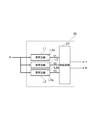
- FIG. 1 shows an FPGA (Field Programmable Gate Array) 10 used in this embodiment.
- FPGA Field Programmable Gate Array
- the FPGA 10 is a device that can change arithmetic functions such as a communication processing function, an encryption processing function, and an image processing function.
- the FPGA 10 includes a basic logic block 11, a DSP block 12, a block RAM 13, an IO block (Input / Output block) in order to realize a desired calculation function in accordance with the type of signal to be calculated and the content of the calculation process. 14, PLL block 15 and the like are provided as circuit blocks (circuit elements).
- the FPGA 10 is provided with a configuration memory 16 and wiring resources (not shown) for connecting the circuit blocks.
- the basic logic block 11 is a basic circuit block constituting the FPGA 10, and is also referred to as a CLB (Configurable Logic Block), a logic element (Logic Element), a logic cell (Logic Cell), or the like.
- the basic logic block 11 has various configurations, but in general, a plurality of basic circuits having a LUT (Lookup table) and a register (flip-flop) as basic elements (sometimes referred to as a slice or the like). It is composed of
- the DSP block 12 is not a combination of the basic logic blocks 11, but is a circuit block that is incorporated in advance as hardware (hardware macro) in order to process operations such as multiplication and product-sum operations at high speed. Sometimes called.
- the DSP block 12 is composed of a high-speed multiplier and adder as basic elements.
- the block RAM 13 is a circuit block that can be used as a general memory. The block RAM 13 is used, for example, when temporarily storing data that is being output from other circuit blocks.
- the IO block 14 is a circuit block that provides an input function and an output function of the FPGA 10.
- the PLL block 15 generates a clock necessary for the operation of the circuit block.
- the wiring resource is composed of a wiring connecting circuit blocks and a pass transistor provided on the wiring.
- Configuration information 18 is loaded (written) into the configuration memory 16.
- the configuration information 18 defines the operation of the circuit block, the connection between the circuit blocks by wiring resources, and is called configuration data, a bit stream, or the like.
- a desired arithmetic circuit is formed in the FPGA 10 according to the configuration information 18.
- the FPGA 10 is a device in which the combination of a plurality of circuit blocks is changed in accordance with the configuration information 18 and the arithmetic function can be changed thereby.
- the FPGA 10 loads the configuration information 18 having the same calculation function and forms a plurality of calculation circuits having different combinations and connection states of circuit blocks into the configuration memory 16.
- arithmetic circuits L1 to L3 and a verification circuit 21 are formed. That is, at least a first arithmetic circuit and a second arithmetic circuit are formed in the FPGA 10. Further, in the arithmetic circuits L1 to L3, output units L1a to L3a for outputting the operation results of the corresponding operation circuits are formed in the verification circuit 21 for verifying the operation results, respectively.
- the configuration information 18 may be loaded into the configuration memory 16 from an external computer, or may be automatically loaded from a nonvolatile memory in which the configuration information 18 is written in advance.
- p (p ⁇ 1) -bit input data X (x 1 to x p ) is input to the FPGA 10 in this example.
- the input data X is not limited to representing one value.
- a plurality of detection values may be combined into the input data X.
- the total number of bits of the plurality of detection values is p bits.
- the input data X may be, for example, one or more sets of numerical values generated by a computer, data received via a network, timing signals for controlling driving of various devices, and the like.
- the above input data X is input to the arithmetic circuits L1 to L3 in the FPGA 10, respectively.
- the arithmetic circuit L1 performs a predetermined operation and outputs q (q ⁇ 1) bits of operation result data V1 (v 11 to v 1q ).
- a predetermined calculation is performed, and calculation result data V2 (v 21 to v 2q ) and V3 (v 31 to v 3q ) are output. .
- the arithmetic circuits L1 to L3 have the same arithmetic function, but in order to improve the error detection rate, the combinations and connection states of the circuit blocks are different from each other. That is, the arithmetic circuits L1 to L3 have different types and numbers of circuit blocks to be used, how to use LUTs and registers in the circuit blocks, and the connection states of these circuit blocks in the arithmetic circuits L1 to L3. However, when no error occurs in the arithmetic circuits L1 to L3, the arithmetic circuits L1 to L3 are configured to output the same arithmetic result data V1 to V3 in response to the input of the same input data X. . From the viewpoint that the combination and connection state of the circuit blocks are different from each other, the arithmetic circuits L1 to L3 are in a relationship between the first arithmetic circuit and the second arithmetic circuit.
- the arithmetic circuits L1 and L3 have a circuit configuration in which at least one DSP block 12 is included in a plurality of circuit blocks to be combined.
- the arithmetic circuit L2 has a circuit configuration in which circuit blocks other than the DSP block 12 are combined (for example, a circuit configuration mainly including the basic logic block 11 including the LUT). Therefore, from the viewpoint of whether or not the circuit configuration includes the DSP block 12, the arithmetic circuits L1 and L3 correspond to the first arithmetic circuit, and the arithmetic circuit L2 corresponds to the second arithmetic circuit.
- the arithmetic circuit L1 and the arithmetic circuit L2 use, for example, a block RAM 13 as a memory for holding data being calculated (hereinafter referred to as a data holding memory), whereas the arithmetic circuit L3 has a basic logic block 11 configuration.
- a block RAM 13 as a memory for holding data being calculated
- the arithmetic circuit L3 has a basic logic block 11 configuration.
- This is a combination of circuit blocks using a so-called distributed RAM using flip-flops. In this way, the arithmetic circuits L1 to L3 use different types of circuit blocks, and the combinations of the circuit blocks are different from each other.
- the DSP block 12 When the DSP block 12 is used like the arithmetic circuits L1 and L3, the number of the basic logic blocks 11 used is greatly reduced compared to the case where the DSP block 12 is not used like the arithmetic circuit L2.
- the combination of the circuit blocks 11 forming the arithmetic circuit including the length of the wiring connecting the circuit blocks can be greatly varied. That is, the arithmetic circuits L1 and L3 and the arithmetic circuit L2 have the same logical arithmetic function, but the operation at the gate level (physical process of signal processing, behavior inside the element at the physical property level, etc.) is greatly different.
- the verification circuit 21 is formed in the FPGA 10 by combining a plurality of circuit blocks.
- the output units L1a to L3a send the operation result data V1 to V3 to the verification circuit 21.
- the verification circuit 21 verifies the operation result data V1 to V3, and generates verification data R as the verification result. Further, when the verification circuit 21 estimates that there is no error among the calculation result data V1 to V3, the verification circuit 21 generates output data Y (y 1 to y q ) as calculation result data.
- the verification circuit 21 outputs verification data R and output data Y to a system controller (not shown) of the control system.
- the verification circuit 21 determines the output data Y by, for example, a majority method. That is, the values of the operation result data V1 to V3 are compared to determine whether they match or not, and the operation result data with the largest number of operation result data having the same value is set as a normal value, and the normal value is output data Y Output as.
- the arithmetic result data V1 to V3 obtained from the arithmetic circuits L1 to L3 all match. Further, when an error occurs only in the arithmetic circuit L1 among the arithmetic circuits L1 to L3, for example, the arithmetic result data V2 and V3 obtained from the arithmetic circuits L2 and L3, and the arithmetic result data V1 obtained from the arithmetic circuit L1 Will be different.
- the arithmetic result data V2 and V3 obtained from the arithmetic circuits L2 and L3 and the arithmetic result data obtained from the arithmetic circuit L1 V1 is different.
- the FPGA 10 has a circuit configuration in which the combinations of the circuit blocks are different from each other in the arithmetic circuits L1 to L3 as described above, so that even if an error occurs due to a common factor of temperature fluctuation, voltage fluctuation, and clock fluctuation, Since the operation states in the operation circuits L1 to L3 with respect to the factors are different, the operation result data V1 to V3 obtained from the operation circuits L1 to L3 are different from each other.
- the FPGA 10 can determine that no error has occurred in the FPGA 10 when all the operation result data V1 to V3 obtained from the operation circuits L1 to L3 match, and each operation obtained from the operation circuits L1 to L3. When the result data V1 to V3 do not match, it can be determined that an error has occurred in the FPGA 10.
- the verification data R is information that serves as an index for determining the error occurrence status and the accuracy of the output data Y.
- the verification data R includes individual verification data R1 to R3 corresponding to the operation result data V1 to V3.
- the individual verification data R1 to R3 indicate in the output data Y, for example, the number of error bits in the corresponding operation result data V1 to V3 and the number of error bits when the output data Y is a normal value. It has information such as the difference between the calculated value and the calculation result data.
- the system controller estimates that the number of calculation result data that does not match the normal value, the number of bits in the mismatch calculation result data, and an error have occurred. Any of the operation circuits to be obtained can acquire information such as the difference between the value of the calculation result data and the normal value that are inconsistent, and the maximum value, minimum value, width, etc. of the difference.
- the configuration information 18 loaded into the FPGA 10 is generated by the configuration information generation device 24.
- the configuration information generation device 24 generates configuration information 18 from the circuit description information 26.
- the circuit description information 26 is a description of arithmetic function specifications abstracted at a register transfer level (Register transfer level, RTL) using a hardware description language (HDL).
- the circuit description information 26 includes verification circuit description information 26a described corresponding to the verification circuit 21 and arithmetic circuit description information 26b.
- the circuit description information 26b For the plurality of arithmetic circuits L1 to L3 (FIG. 2), For example, one arithmetic circuit description information 26b is commonly used. It is described using FBD (Function Block Diagram) language used for industrial applications, etc., and high-level synthesis is performed on hardware description information with higher abstraction level (behavioral level). Then, the circuit description information 26 at the register transfer level may be generated.
- FBD Field Block Diagram
- the configuration information generation device 24 includes a logic synthesis unit 24a, a synthesis parameter setting unit 24b, a combining unit 24c, and a mapping unit 24d.
- the logic synthesis unit 24a, the coupling unit 24c, and the mapping unit 24d are realized by installing an application program known as a logic synthesis tool or the like in a computer.
- the synthesis parameter setting unit 24b is configured to change a synthesis parameter related to logic synthesis of the logic synthesis tool.
- the synthesis parameter specifies conditions for forming the arithmetic circuits L1 to L3 in the FPGA 10, and the conditions regarding the combination of circuit blocks can be changed by the synthesis parameters.
- the logic synthesis unit 24 a performs logic synthesis for generating a net list from the circuit description information 26.
- the netlist describes the wiring and the like for connecting the circuit blocks.
- the synthesis parameter setting unit 24b sets parameter sets P 0 to P 3 when the logic synthesis unit 24a performs logic synthesis.
- the parameter set P 0 is a set of a plurality of synthesis parameters set so that the combination of circuit blocks is optimized for the verification circuit 21. This parameter set P 0 is used when generating the net list N 0 of the verification circuit 21 from the verification circuit description information 26a.
- each of the parameter sets P 1 to P 3 is a set of a plurality of synthesis parameters when the arithmetic circuit description information 26b is embodied in a combination of circuit blocks.
- These parameter sets P 1 to P 3 include several synthesis parameters in order to generate the arithmetic circuits L1 to L3 having different combinations of circuit blocks as described above from the same arithmetic circuit description information 26b. The settings are different.
- the parameter sets P 1 to P 3 include synthesis parameters relating to the use of the DSP block 12 (hereinafter referred to as DSP parameters) and synthesis parameters relating to the data holding memory (hereinafter referred to as memory parameters).
- DSP parameters synthesis parameters relating to the use of the DSP block 12
- memory parameters synthesis parameters relating to the data holding memory
- Parameter set P 1 is for generating the netlist N 1 arithmetic circuit L1.
- the DSP parameter of the parameter set P 1 is a setting value that uses the DSP block 12 to the maximum extent.
- the memory parameter in the parameter set P 1 is adapted to set value using the block RAM13 as data memory.
- Parameter set P 2 is for generating a netlist N 2 arithmetic circuit L2.
- DSP parameters of this parameter set P 2 is the set value without using the DSP block 12, also a memory parameter is adapted to set value using the block RAM13 as data memory.
- the parameter set P 3 is for generating a netlist N 3 of the arithmetic circuit L3.
- DSP parameters of this parameter set P 3 is a set value for maximum use of the DSP block 12, also a memory parameter is adapted to set value using distributed RAM as data memory.
- the synthesis parameter setting unit 24b sets the parameter sets P 1 to P 3 in the logic synthesis unit 24a during logic synthesis for the operation circuits L1 to L3, thereby forming the operation circuits L1 to L3.
- Conditions relating to the combination of circuit blocks (FPGA resources) are given, and the circuit blocks of the arithmetic circuits L1 to L3 are made different from each other to give diversity to the arithmetic circuits L1 to L3.
- Logic synthesis unit 24a by performing logic synthesis under composition parameter set P 0, to generate a net list N 0 from the verification circuit description information 26a.
- the logic synthesis unit 24a generates netlists N 1 to N 3 by performing logic synthesis using the operation circuit description information 26b under the synthesis parameter sets P 1 to P 3 , respectively.
- the arithmetic circuits L1 to L3 have different combinations of circuit blocks, even if the input data X is input at the same timing between the arithmetic circuits L1 to L3, the operation result data V1 to V3 are output. Timing may be different. In such a case, for example, a delay circuit may be formed so that the input timing of the operation result data V1 to V3 to the verification circuit 21 is the same.
- the combining unit 24c combines the four net lists N 0 to N 3 obtained from the logic synthesis unit 24a into one net list. At the time of this combination, the combining unit 24c generates a net list in which three sets of output terminals shown in the net lists N 1 to N 3 are connected to three sets of input terminals of the net list N 0 .
- the mapping unit 24d performs so-called mapping (placement wiring) that allocates connections shown in the net list to circuit blocks and input / output pins of the FPGA 10 according to the net list from the coupling unit 24c.
- the mapping unit 24 d outputs the mapped information as configuration information 18 to the configuration memory 16 of the FPGA 10.
- the configuration information 18 includes verification circuit configuration information C 0 for forming the verification circuit 21 and arithmetic circuit configuration information C 1 to C 3 for forming the arithmetic circuits L1 to L3.
- the verification circuit description information 26a and the arithmetic circuit description information 26b common to the arithmetic circuits L1 to L3 are prepared, and the configuration information generation device 24 generates the configuration information 18 based on these.
- synthesis parameter setting unit 24b sets a parameter set P 0 to the first logical combining unit 24a.
- logic synthesis unit 24a reads the verification circuit description information 26a, performs logical synthesis under the parameter set P 0, to generate a net list N 0 from the verification circuit description information 26a.
- the synthesis parameter setting unit 24b sets a parameter set P 1 to the logic synthesizing section 24a. Thereafter, logic synthesis unit 24a reads the arithmetic circuit description information 26b, by performing logic synthesis under parameter set P 1, to generate a net list N 1 from the arithmetic circuit description information 26b.
- the DSP parameter of the parameter set P 1 is a setting value that uses the DSP block 12 as much as possible
- the memory parameter is a setting value that uses the block RAM 13 as a data holding memory. Accordingly, the arithmetic circuit description information 26b to realize a predetermined calculation function, the parameters under set P 1, the DSP block 12 maximally used, and the net combination of circuit blocks using block RAM13 as data memory It is converted to a list N 1.
- the parameter set P 2 is set by the synthesis parameter setting unit 24b. Thereafter, logic synthesis unit 24a reads the arithmetic circuit description information 26b, by performing logic synthesis under the parameter set P 2, to produce a netlist N 2 from the arithmetic circuit description information 26b.
- the DSP parameter is a setting value that does not use the DSP block 12
- the memory parameter is a setting value that uses the block RAM 13 as a data holding memory.
- the arithmetic circuit description information 26b to realize a predetermined calculation function, under the parameter set P 2, without using the DSP block 12, and the net list of the combinations of circuit blocks using block RAM13 as a data holding memory N Is converted to 2 .
- the parameter set P 3 is set in the logic synthesis unit 24 a by the synthesis parameter setting unit 24 b. Thereafter, logic synthesis unit 24a, the arithmetic circuit description information 26b is read into the logic synthesis unit 24a, under the parameter set P 3, to produce a netlist N 3 from the arithmetic circuit description information 26b.
- the DSP parameter is a setting value that uses the DSP block 12 as much as possible
- the memory parameter is a setting value that uses the distributed RAM as the data holding memory.
- the configuration information 18 from the mapping unit 24d is loaded into the configuration memory 16 of the FPGA 10.
- arithmetic circuits L1 to L3 and a verification circuit 21 are formed in the FPGA 10.
- the arithmetic circuits L1 to L3 have the same arithmetic function, but the combinations of circuit blocks are different from each other.
- the arithmetic circuits L1 and L3 are combinations of circuit blocks that use the DSP block 12 to the maximum, whereas the arithmetic circuit L2 is a combination of circuit blocks other than the DSP block 12.
- the arithmetic circuits L1 and L2 use a block RAM 13 as a data holding memory, whereas the arithmetic circuit L3 is a combination of circuit blocks using a distributed RAM as a data holding memory.
- the configuration information generation device 24 performs logic synthesis under the synthesis parameters, and uses the same arithmetic circuit description information 26b.
- Netlists N 1 to N 3 corresponding to the arithmetic circuits L1 to L3 are generated, and configuration information 18 including the arithmetic circuit configuration information C 1 to C 3 is generated using the net lists N 1 to N 3 .
- the arithmetic circuits L1 to L3 and the verification circuit 21 are formed as described above, when input data X is input, the input data X is input to the arithmetic circuits L1 to L3, respectively.
- the arithmetic circuit L1 performs an operation on the input data X, and outputs the operation result data V1 obtained as a result to the verification circuit 21.
- the operation circuits L2 and L3 perform operations on the input data X, and output the operation result data V2 and V3 obtained as a result to the verification circuit 21, respectively.
- the FPGA 10 generates a plurality of calculation result data V 1 to V 3 for one input data X, and inputs these calculation result data V 1 to V 3 to the verification circuit 21.
- the verification circuit 21 compares the operation result data V1 to V3 each time the operation result data V1 to V3 are input as described above. Then, when all the operation result data V1 to V3 match, the verification circuit 21 outputs any one of the operation result data as output data Y to the system controller. Further, the verification circuit 21 generates individual verification data R1 to R3 indicating that the calculation result data V1 to V3 are the same data as the output data Y, and the individual verification data R1. The verification data R including .about.R3 is also output to the system controller.
- the verification circuit 21 when only two of the operation result data V1 to V3 match, the verification circuit 21 outputs one of the two calculated operation result data as output data Y to the system controller. For example, if the calculation result data V1 and V3 match and the calculation result data V2 does not match, one of the calculation result data V1 and V3 is output as output data Y from the verification circuit 21 to the system controller. . At this time, the verification circuit 21 generates individual verification data R1 and R3 indicating that the calculation result data V1 and V3 are the same data as the output data Y, and the calculation result data V2 is different from the output data Y. Individual verification data R2 having information indicating bits to be generated is generated, and verification data R including the individual verification data R1 to R3 is output to the system controller.
- the verification circuit 21 If all of the operation result data V1 to V3 do not match, the verification circuit 21 outputs a specified value as output data Y to the system controller, for example. In this case, the verification circuit 21 generates individual verification data R1 to R3 indicating that the operation result data V1 to V3 do not match, and the verification data R including the individual verification data R1 to R3 is generated. Output to the system controller.
- a plurality of arithmetic circuits having the same arithmetic function and the combination of the same circuit blocks are formed to perform error verification. If an error has occurred in each arithmetic circuit due to a common cause of voltage fluctuation and clock fluctuation, the operation status of each arithmetic circuit for the common factor will be the same. The state will be the same. For this reason, in the conventional FPGA error verification method, each arithmetic circuit generates the same operation result data, and therefore, it is difficult to detect that an error has occurred because all of the operation result data match. It was.
- the FPGA 10 of this embodiment although the arithmetic circuits L1 to L3 have the same arithmetic function as described above, the combinations of circuit blocks constituting the arithmetic circuits L1 to L3 are different from each other.
- the operation states of the arithmetic circuits L1 to L3 are different, and the occurrence states of errors occurring in the arithmetic circuits L1 to L3 are also different.
- the arithmetic circuits L1 to L3 may simultaneously generate the same arithmetic result data V1 to V3.
- the calculation result data V1 to V3 are very unlikely to be inconsistent. Therefore, the FPGA 10 can detect an error based on the determination result of the verification circuit 21 that the operation result data V1 to V3 do not match.
- errors may occur in all the arithmetic circuits L1 to L3 as described above, or combinations of circuit blocks constituting the arithmetic circuits L1 to L3 are different from each other.
- An error may occur in one or two of the arithmetic circuits L1 to L3, and no error may occur in other arithmetic circuits.
- the arithmetic circuits L1 to L3 do not generate the same arithmetic result data V1 to V3 at the same time, so that the arithmetic result data V1 to V3 are inconsistent, and the verification circuit 21 is based on this result. Can detect errors.
- the FPGA 10 can detect an error based on the determination result of the verification circuit 21 that the operation result data V1 to V3 do not match.
- the error detection rate based on the calculation result data V1 to V3 from the plurality of calculation circuits L1 to L3 having the same calculation function and various combinations of circuit blocks is the same as the conventional calculation. This is higher than when redundancy is provided by a plurality of arithmetic circuits having functions and combining the same circuit blocks.
- the mode for making the combination of the circuit blocks of the plurality of arithmetic circuits L1 to L3 described above different from each other is an example and is not limited to the above.
- the DSP block 12 when there are two arithmetic circuits, only whether or not the DSP block 12 is used may be different as in the relation between the arithmetic circuit L1 and the arithmetic circuit L2.
- the number of DSP blocks 12 used in each of the plurality of arithmetic circuits L1 to L3 and the ratio of the number of DSP blocks 12 to the total number of circuit blocks forming the arithmetic circuits L1 to L3 may be different.
- the present invention is not limited to the DSP block 12, and for example, whether or not a specific hard macro such as a multiplier is used, the number and ratio thereof may be different.
- the verification circuit 21 is formed in the FPGA 10, but without the verification circuit 21 being formed in the FPGA 10, the operation result data of each of the operation circuits L1 to L3 is directly output from the FPGA 10 to an external device. You may comprise. In this case, verification similar to that performed by the verification circuit 21 may be performed in an external device.
- the method of determining the output data Y in the verification circuit 21 is an example. For example, the operation result data having the largest value may be used as the output data Y (high value selection). Conversely, the operation result data having a small value may be used as the output data Y (low value selection).
- an average value or an intermediate value of each calculation result data may be set as the output data Y, or a value of calculation result data exceeding a certain number, for example, a majority, may be set as the output data Y (conditional majority decision).
- the distribution of the values of each calculation result data is calculated, and high value selection, low value selection, average value, intermediate value, majority vote, conditional majority vote, etc. are calculated from the calculation result data out of the specific deviation range. You may go. Further, the above methods may be combined when determining the output data Y. In the case of conditional majority, if there is no calculation result data exceeding a certain number, a specified value can be output as output data Y.
- the selected bit value may be assigned to the bit of the output data Y by performing a majority vote, a conditional majority vote or the like between corresponding bits of each operation result data. Also, a reference bit string obtained by performing majority vote, conditional majority vote, etc. between corresponding bits of each operation result data is generated, and the corresponding bits of the reference bit string and the bit string of each operation result data are compared with each other. A small amount of calculation result data may be output data Y.
- the operation description information of the multiplication function described in the FBD language which is a control description language compliant with IEC-61131, mounted on the plant control apparatus is synthesized at a high level, and the arithmetic circuit description information by Verilog HDL was generated.
- logic synthesis was performed using two different parameter sets to generate net lists N 1 and N 2 corresponding to the two arithmetic circuits L1 and L2, respectively.
- the netlists N 1 and N 2 were combined into one netlist and mapped based on the netlist to obtain configuration information 18.
- the timing simulation is performed on the simulation tool using the configuration information 18 and the propagation delay information of the FPGA 10 to be simulated.
- ISE registered trademark
- FPGA 10 is XC7K325T-2 (Kintex-7, manufactured by Xilinx).
- the calculation performed by the calculation circuits L1 and L2 in the verification example is a multiplication of two input values (integers).
- the two input values are generated by random numbers, and these two input values are input to the arithmetic circuits L1 and L2 as one input data X, respectively.
- the calculation result data V1 and V2 obtained from the calculation circuits L1 and L2 are 32 bits, respectively.
- the DSP parameter of the setting value that uses the DSP block 12 to the maximum is used, and in the logic synthesis for generating the netlist N 2 , the DSP parameter of the setting value that does not use the DSP block 12 is used.
- the netlists N 1 and N 2 were generated without any particular setting.
- the arithmetic circuit L1 of the verification example has a circuit configuration in which the DSP block 12 is used to the maximum extent.
- the arithmetic circuit L2 of the verification example has a circuit configuration in which circuit blocks other than the DSP block 12 are combined.
- Table 1 shows the usage state of the circuit blocks of the arithmetic circuits L1 and L2 as a verification example.
- Table 1 shows, as another verification example, the use state of the circuit block in the case where the arithmetic circuits L1 and L2 are configured to perform proportional-integral calculation with the same synthesis parameter setting.
- the “slice” is a basic circuit that constitutes the above-described basic configuration block, and includes a LUT and a register (flip-flop) as basic elements.
- the error occurrence situation in the actual environment resembles the situation where the operating frequency of the FPGA 10 fluctuated.
- a state similar to a state in which a signal propagation delay occurs between each circuit block due to temperature variation or voltage variation is generated by changing the operating frequency of the FPGA 10 on the simulation.
- the operating frequency is changed by 2 MHz from 160 MHz to 258 MHz, and the multiplication operation is executed by the arithmetic circuits L1 and L2 at each operating frequency.
- Fig. 4 shows the relationship between the error rate and the operating frequency in the above verification example.
- the horizontal axis of the graph of FIG. 4 is the operating frequency of the FPGA 10, and the vertical axis is the error occurrence rate.
- the number of error occurrences is counted when at least one of the operation result data V1 and V2 becomes an incorrect value, and the error occurrence rate is calculated based on the input data X for each operating frequency.
- the ratio (%) of the number of error occurrences to the number of inputs (10,000 times). Whether or not the calculation result data V1 and V2 have incorrect values is determined by comparing the true value calculated separately and the calculation result data V1 and V2.
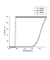
- FIG. 5 shows the error detection rate due to the mismatch between the calculation result data V1 and V2.
- the horizontal axis of the graph of FIG. 5 is the operating frequency of the FPGA 10, and the vertical axis is the error detection rate.
- the number of times of error detection is counted assuming that the calculation result data V1 and V2 do not coincide with each other, and the error detection rate is the number of inputs of the input data X for each operating frequency (1 The ratio (%) of error detection times to (10,000 times).
- FIG. 5 shows the result of verification at an operating frequency of 178 MHz or higher in which an error was detected in Comparative Example 1 described later.
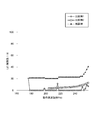
- FIG. 6 shows the distance between the calculation result data V1 and V2 (hereinafter referred to as the mismatch distance).
- the mismatch distance (D) is obtained by dividing the sum of error bits normalized by 32 bits by the number of times of error detection at the operating frequency for each operating frequency. Indicated by The mismatch distance increases when the difference between the calculation result data V1 and V2 is large.
- E (i, f) in the above equation (1) is the number of bits that do not match between the operation result data V1 and V2 for the i-th input data X at the operating frequency f.
- S (f) is the number of times of error detection at the operating frequency f.
- Comparative Example 1 a timing simulation for an FPGA in which two arithmetic circuits L1 in which the DSP block 12 is used to the maximum is formed is referred to as Comparative Example 1.
- Comparative Example 2 A timing simulation of an FPGA in which two arithmetic circuits L2 formed by combining circuit blocks are formed is referred to as Comparative Example 2.
- the configuration information for forming the arithmetic circuits L1 and L2 in the FPGAs of Comparative Example 1 and Comparative Example 2 was generated in the same manner as in the verification example. And also about the comparative example 1 and the comparative example 2, the timing simulation was performed on the simulation tool similarly to the verification example.
- the verification results of Comparative Example 1 and Comparative Example 2 are also shown in FIGS.
- Comparative Example 1 From the above, in Comparative Example 1, it can be seen that the operation result data output from at least one of the two operation circuits L1 has an incorrect value at an operating frequency of 178 MHz or higher. However, as shown in FIG. 5, in Comparative Example 1, errors are detected at several operating frequencies of 178 MHz or higher, but errors are not detected at other operating frequencies. This is because, in Comparative Example 1, two arithmetic circuits L1 composed of the same circuit block combination are used, so that the same error occurs in each of the two arithmetic circuits L1, and the respective arithmetic operations to be output This is because the result data is exactly the same and as a result cannot be detected as an error. In Comparative Example 2, the error detection rate is almost 100%, but at the operating frequency above 218 MHz, a decrease in the error detection rate of about 1 to 2% was observed.
- the error detection rate of the verification example according to the present invention was 100% at all operating frequencies. That is, rather than a configuration in which a plurality of arithmetic circuits having the same combination of circuit blocks are made redundant as in Comparative Example 1 and Comparative Example 2, a plurality of arithmetic circuits L1 having different combinations of circuit blocks as in the verification example of the present invention. L2, that is, by using a configuration in which a plurality of arithmetic circuits having diversity are formed, it has been confirmed that errors can be detected more reliably, thus improving the error detection rate. Further, as shown in FIG. 6, it was confirmed that the mismatch distance in the verification example was three times or more larger than that in Comparative Example 1 and Comparative Example 2.
Landscapes
- Engineering & Computer Science (AREA)
- Physics & Mathematics (AREA)
- General Physics & Mathematics (AREA)
- Theoretical Computer Science (AREA)
- Computing Systems (AREA)
- General Engineering & Computer Science (AREA)
- Mathematical Analysis (AREA)
- Pure & Applied Mathematics (AREA)
- Mathematical Optimization (AREA)
- Computational Mathematics (AREA)
- Mathematical Physics (AREA)
- Computer Hardware Design (AREA)
- Nonlinear Science (AREA)
- Logic Circuits (AREA)
Abstract
La présente invention forme des circuits d'opération arithmétique (L1-L3) et un circuit de vérification (21) en chargeant des informations de configuration dans la mémoire de configuration d'un réseau prédiffusé programmable par l'utilisateur (10). Bien que les circuits d'opération arithmétique (L1-L3) aient la même fonction d'opération arithmétique, ils diffèrent les uns des autres dans leurs combinaisons de blocs de circuit. Les circuits d'opération arithmétique (L1 et L3) présentent une combinaison de blocs de circuit dans laquelle le nombre maximum de blocs DSP (12) est utilisé, et le circuit d'opération arithmétique (L2) présente une combinaison de blocs de circuit ne comprenant aucun bloc DSP (12). Les circuits d'opération arithmétique (L1 et L2) utilisent un bloc de mémoire RAM (13) en tant que mémoire de stockage de données, et le circuit d'opération arithmétique (L3) utilise une mémoire RAM répartie en tant que mémoire de stockage de données. Des données d'entrée (X) sont entrées dans chacun des circuits d'opération arithmétique (L1-L3), qui délivrent en sortie des données de résultats d'opération arithmétique (V1-V3). Le circuit de vérification compare (21) les données de résultats d'opération arithmétique (V1-V3) et vérifie s'il y a une erreur.
Priority Applications (2)
| Application Number | Priority Date | Filing Date | Title |
|---|---|---|---|
| US15/572,140 US10067742B2 (en) | 2015-05-07 | 2016-02-24 | Programmable logic device, method for verifying error of programmable logic device, and method for forming circuit of programmable logic device |
| EP16789468.2A EP3293883B1 (fr) | 2015-05-07 | 2016-02-24 | Dispositif à logique programmable, procédé de vérification d'erreur de dispositif à logique programmable, et procédé de formation de circuit de dispositif à logique programmable |
Applications Claiming Priority (2)
| Application Number | Priority Date | Filing Date | Title |
|---|---|---|---|
| JP2015094970A JP5807887B1 (ja) | 2015-05-07 | 2015-05-07 | プログラマブルロジックデバイス、プログラマブルロジックデバイスのエラー検証方法、及びプログラマブルロジックデバイスの回路形成方法 |
| JP2015-094970 | 2015-05-07 |
Publications (1)
| Publication Number | Publication Date |
|---|---|
| WO2016178332A1 true WO2016178332A1 (fr) | 2016-11-10 |
Family
ID=54545798
Family Applications (1)
| Application Number | Title | Priority Date | Filing Date |
|---|---|---|---|
| PCT/JP2016/055389 Ceased WO2016178332A1 (fr) | 2015-05-07 | 2016-02-24 | Dispositif à logique programmable, procédé de vérification d'erreur de dispositif à logique programmable, et procédé de formation de circuit de dispositif à logique programmable |
Country Status (4)
| Country | Link |
|---|---|
| US (1) | US10067742B2 (fr) |
| EP (1) | EP3293883B1 (fr) |
| JP (1) | JP5807887B1 (fr) |
| WO (1) | WO2016178332A1 (fr) |
Families Citing this family (4)
| Publication number | Priority date | Publication date | Assignee | Title |
|---|---|---|---|---|
| JP6696352B2 (ja) * | 2016-08-18 | 2020-05-20 | 富士通株式会社 | プログラマブルロジック装置、情報処理装置、処理方法、及び処理プログラム |
| KR102525165B1 (ko) * | 2018-12-18 | 2023-04-24 | 삼성전자주식회사 | 연산 회로를 포함하는 비휘발성 메모리 장치 및 이를 포함하는 뉴럴 네트워크 시스템 |
| CN110096397B (zh) * | 2019-03-27 | 2022-10-25 | 天津大学 | 基于多环形振荡器fpga配置电路鲁棒性检测方法 |
| WO2025080293A2 (fr) * | 2023-05-12 | 2025-04-17 | Massachusetts Institute Of Technology | Processeur 3d |
Citations (2)
| Publication number | Priority date | Publication date | Assignee | Title |
|---|---|---|---|---|
| JP2001099627A (ja) * | 1999-07-23 | 2001-04-13 | Matsushita Electric Works Ltd | 画像処理システムおよびその構成方法 |
| JP2011216020A (ja) * | 2010-04-01 | 2011-10-27 | Mitsubishi Electric Corp | 情報処理装置および回路再構成装置 |
Family Cites Families (8)
| Publication number | Priority date | Publication date | Assignee | Title |
|---|---|---|---|---|
| JP5310036B2 (ja) * | 2009-01-30 | 2013-10-09 | 富士通株式会社 | 検証支援プログラムおよび検証支援装置 |
| US8949609B2 (en) * | 2009-07-13 | 2015-02-03 | Nec Corporation | Anonymous authentication signature system, user device, verification device, signature method, verification method, and program therefor |
| NL1037275C2 (nl) * | 2009-09-11 | 2011-03-14 | Advanced Public Transp Systems B V | Stuurinrichting voor een vooraf gedefinieerd traject verplaatsbaar voertuig, automatisch gestuurd en via tenminste een eerste as , alsmede een voertuig voorzien van een dergelijke stuurinrichting. |
| US8365131B2 (en) * | 2010-01-11 | 2013-01-29 | Empire Technology Development Llc | Hardware synthesis using thermally aware scheduling and binding |
| JP2012043197A (ja) * | 2010-08-19 | 2012-03-01 | Toshiba Tec Corp | 情報処理装置及びプログラム |
| US20140237263A1 (en) * | 2013-02-19 | 2014-08-21 | Kabushiki Kaisha Toshiba | Nonvolatile semiconductor memory device and memory system using the same |
| US8769450B1 (en) * | 2013-06-28 | 2014-07-01 | Xilinx, Inc. | Synthesis flow for formal verification |
| JP6528612B2 (ja) * | 2015-08-31 | 2019-06-12 | 株式会社ソシオネクスト | 電源電圧制御回路、電源電圧制御方法および電源電圧制御プログラム |
-
2015
- 2015-05-07 JP JP2015094970A patent/JP5807887B1/ja active Active
-
2016
- 2016-02-24 US US15/572,140 patent/US10067742B2/en active Active
- 2016-02-24 WO PCT/JP2016/055389 patent/WO2016178332A1/fr not_active Ceased
- 2016-02-24 EP EP16789468.2A patent/EP3293883B1/fr active Active
Patent Citations (2)
| Publication number | Priority date | Publication date | Assignee | Title |
|---|---|---|---|---|
| JP2001099627A (ja) * | 1999-07-23 | 2001-04-13 | Matsushita Electric Works Ltd | 画像処理システムおよびその構成方法 |
| JP2011216020A (ja) * | 2010-04-01 | 2011-10-27 | Mitsubishi Electric Corp | 情報処理装置および回路再構成装置 |
Non-Patent Citations (1)
| Title |
|---|
| See also references of EP3293883A4 * |
Also Published As
| Publication number | Publication date |
|---|---|
| US20180129471A1 (en) | 2018-05-10 |
| JP2016213637A (ja) | 2016-12-15 |
| JP5807887B1 (ja) | 2015-11-10 |
| EP3293883A1 (fr) | 2018-03-14 |
| US10067742B2 (en) | 2018-09-04 |
| EP3293883B1 (fr) | 2020-11-18 |
| EP3293883A4 (fr) | 2018-12-19 |
Similar Documents
| Publication | Publication Date | Title |
|---|---|---|
| US10289483B2 (en) | Methods and apparatus for embedding an error correction code in storage circuits | |
| US8997033B1 (en) | Techniques for generating a single configuration file for multiple partial reconfiguration regions | |
| JP6363297B2 (ja) | シミュレータ、半導体回路装置の設計支援システムおよび方法 | |
| US11748548B2 (en) | Hierarchical clock tree implementation | |
| EP3324317B1 (fr) | Procédés de vérification de circuits recalés avec initialisation temporisée | |
| US20100313176A1 (en) | Delay library, delay library creation method, and delay calculation method | |
| CN112069763B (zh) | 修正电路的方法 | |
| US8984462B1 (en) | Physical optimization for timing closure for an integrated circuit | |
| JP5807887B1 (ja) | プログラマブルロジックデバイス、プログラマブルロジックデバイスのエラー検証方法、及びプログラマブルロジックデバイスの回路形成方法 | |
| US8977998B1 (en) | Timing analysis with end-of-life pessimism removal | |
| US10302698B1 (en) | Estimation of power consumed by combinatorial circuitry | |
| US10162916B1 (en) | Timing verification in a programmable circuit design using variation factors | |
| US8813018B1 (en) | Method and apparatus for automatically configuring memory size | |
| US8893068B1 (en) | Techniques to generate a more accurate simulation model | |
| US10169518B1 (en) | Methods for delaying register reset for retimed circuits | |
| US9672307B2 (en) | Clock placement for programmable logic devices | |
| US9152756B2 (en) | Group based routing in programmable logic device | |
| KR20180051708A (ko) | 스위칭 액티비티에 기초한 반도체 장치의 배치 방법 및 이에 의해 제조된 반도체 장치 | |
| CN118966096A (zh) | 芯片的安全设计方法、电子设备及存储介质 | |
| US8881082B2 (en) | FEC decoder dynamic power optimization | |
| US9268891B1 (en) | Compact and efficient circuit implementation of dynamic ranges in hardware description languages | |
| US10565334B1 (en) | Targeted delay optimization through programmable clock delays | |
| JP7051151B2 (ja) | 数値情報生成装置、数値情報生成方法及びプログラム | |
| US9811503B1 (en) | Methods for implementing arithmetic functions with user-defined input and output formats | |
| US20260093885A1 (en) | Skew balancing among circuit signal pathways |
Legal Events
| Date | Code | Title | Description |
|---|---|---|---|
| 121 | Ep: the epo has been informed by wipo that ep was designated in this application |
Ref document number: 16789468 Country of ref document: EP Kind code of ref document: A1 |
|
| WWE | Wipo information: entry into national phase |
Ref document number: 15572140 Country of ref document: US |
|
| NENP | Non-entry into the national phase |
Ref country code: DE |