WO2016181553A1 - Unité de protection pouvant être montée sur une surface et dispositif électronique la comprenant - Google Patents
Unité de protection pouvant être montée sur une surface et dispositif électronique la comprenant Download PDFInfo
- Publication number
- WO2016181553A1 WO2016181553A1 PCT/JP2015/063927 JP2015063927W WO2016181553A1 WO 2016181553 A1 WO2016181553 A1 WO 2016181553A1 JP 2015063927 W JP2015063927 W JP 2015063927W WO 2016181553 A1 WO2016181553 A1 WO 2016181553A1
- Authority
- WO
- WIPO (PCT)
- Prior art keywords
- partition wall
- frame
- cap
- substrate
- shielding unit
- Prior art date
- Legal status (The legal status is an assumption and is not a legal conclusion. Google has not performed a legal analysis and makes no representation as to the accuracy of the status listed.)
- Ceased
Links
Images


Classifications
-
- H—ELECTRICITY
- H05—ELECTRIC TECHNIQUES NOT OTHERWISE PROVIDED FOR
- H05K—PRINTED CIRCUITS; CASINGS OR CONSTRUCTIONAL DETAILS OF ELECTRIC APPARATUS; MANUFACTURE OF ASSEMBLAGES OF ELECTRICAL COMPONENTS
- H05K9/00—Screening of apparatus or components against electric or magnetic fields
Definitions
- This application relates to a surface mount type shielding unit and an electronic device including the shielding unit.
- Electronic devices having a wireless communication function such as mobile phones, tablet terminals, and mobile PCs include various electronic components such as a high-speed CPU and a memory on the same substrate in addition to wireless components.
- the sensitivity of the wireless component may deteriorate due to radiation noise from the CPU and memory or noise interference between the wireless components.
- the influence of unnecessary radiation noise is reduced by mounting a noise shielding frame unit that covers electronic components on a substrate.
- the noise shielding frame unit includes a small sheet metal frame that independently covers one electronic component that is a noise generation source, and a large sheet metal frame that collectively covers a plurality of electronic components. included.
- the latter frame unit has an internal partition for dividing a space surrounded by the sheet metal frame. Therefore, the latter frame unit may be referred to as a “partitioned” frame unit below. Further, the former frame unit may be hereinafter referred to as a “no partition” frame unit for comparison with a “partition” frame unit.
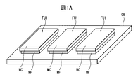
- FIG. 1A is a perspective view showing a circuit board CB on which a frame unit FU1 without partition is mounted.
- 1B is a top view of the circuit board CB and the frame unit FU1 in FIG. 1A
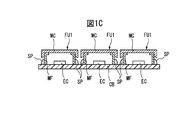
- FIG. 1C is a cross-sectional view taken along line 1C-1C in FIG. 1B.
- three frame units FU1 that independently cover three electronic components EC arranged in the left-right direction are mounted on a circuit board CB.
- the undivided frame unit FU1 has a sheet metal frame MF and a sheet metal cap MC formed in accordance with the dimensions and mounting conditions of the individual electronic components EC.
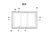
- FIG. 2A is a perspective view showing the circuit board CB on which the frame unit with partition FU2 is mounted.
- 2B is a top view of the circuit board CB and the frame unit FU2 in FIG. 2A
- FIG. 2C is a cross-sectional view taken along line 2C-2C in FIG. 2B.
- a single frame unit FU2 that collectively covers three electronic components EC arranged in the left-right direction is mounted on the circuit board CB.
- the frame unit FU2 with partitions has two internal partitions IP that divide the space surrounded by the sheet metal frame, and each internal partition IP includes the adjacent electronic components EC, It is arranged between ECs.
- the partition-attached frame unit FU2 When the partition-attached frame unit FU2 is used, the clearance between the sheet metal frames is not provided, so that the mounting area on the circuit board CB becomes relatively small.
- a contact failure between the sheet metal cap MP and the internal partition IP may occur due to manufacturing errors such as the internal partition IP and the sheet metal cap MC.
- the sheet metal cap MC may be partially lifted by the internal partition IP due to manufacturing errors such as the internal partition IP and the sheet metal cap MC. The above event will be described with reference to FIGS. 3A to 3D.
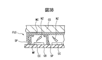
- FIG. 3A is a cross-sectional view showing a circuit board CB on which a frame unit F3 with a partition similar to the frame unit FU2 in FIGS. 2A to 2C is mounted.
- FIG. 3A also shows a device case CS attached above the circuit board CB (the same applies to FIGS. 3B to 3D described later).
- the electromagnetic wave noise NZ radiated from one electronic component EC passes through the internal partition IP to the other electronic component EC.
- the sheet metal cap MC is not lifted by the internal partition IP.
- FIG. 3B is a cross-sectional view similar to FIG. 3A and shows the frame unit FU3 in which the internal partition IP is lower than the sheet metal frame due to manufacturing errors.
- the electromagnetic wave noise NZ radiated from one electronic component EC passes through the internal partition IP to the other electronic component EC. There is a risk of reaching. As a result, noise interference may occur between the adjacent electronic components EC and EC.
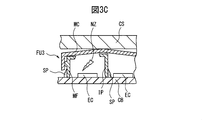
- FIG. 3C is a cross-sectional view similar to FIG. 3A, showing the frame unit FU3 in which the internal partition IP is higher than the sheet metal frame MF due to manufacturing errors. In the example of FIG.
- the height of the gap between the circuit board CB and the device case CS is designed to include a clearance for preventing the sheet metal cap MC from contacting the device case CS.
- the clearance is determined in consideration of the dimensional tolerance of the internal partition IP.
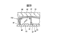
- FIG. 3D is a cross-sectional view similar to FIG. 3A, and shows a frame unit FU3 in which a projection PP is provided on the inner surface of the sheet metal cap MC to ensure contact with the internal partition IP. Also in the example of FIG. 3D, since a part of the sheet metal cap MC is lifted by the internal partition IP, the height of the gap between the circuit board CB and the device case CS is designed to include the clearance. Yes.
- the design in which the height of the gap between the circuit board CB and the device case CS is increased as shown in FIGS. 3C and 3D is disadvantageous in downsizing the device (particularly in reducing the thickness).
- the present invention has been made in view of the above-described problems, and an object of the present invention is a surface mount type that eliminates the lifting of the cap due to the partition wall while ensuring contact between the cap and the partition wall in the frame. Is to provide a shielding unit.
- a frame that surrounds a plurality of electronic components installed on the upper surface of the substrate, a partition wall that partitions a space inside the frame in which the plurality of electronic components are arranged, and a top plate that covers the frame A side plate facing the outer surface of the frame, and a cap having an inclined surface formed so as to be slidably contactable with the partition wall at a position facing the partition wall on the inner surface of the top plate. It has a support part that supports the side plate so that the outer edge of the plate can move in the direction toward or away from the partition wall, and the cap is interlocked with the inclined surface sliding obliquely downward with respect to the partition wall.
- a surface-mount type shielding unit is provided in which the outer edge portion is formed so as to move in a direction toward the partition wall or in a direction away from the partition wall.
- the disclosed shielding unit even if the cap is lifted by the partition wall due to a dimensional error of the partition wall, the lifted portion of the top plate is moved diagonally downward by pressing the top plate toward the substrate. Can be made. Therefore, according to the disclosed shielding unit, it is possible to eliminate the lifting of the cap due to the partition wall while ensuring the contact between the cap and the partition wall.
- FIG. 1A is a perspective view showing a circuit board on which a frame unit without partition is mounted.
- FIG. 1B is a top view of the circuit board and the frame unit in FIG. 1A.
- 1C is a cross-sectional view taken along line 1C-1C in FIG. 1B.
- FIG. 2A is a perspective view showing a circuit board on which a frame unit without partition is mounted.
- 2B is a top view of the circuit board and the frame unit in FIG. 2A.
- 2C is a cross-sectional view taken along line 2C-2C in FIG. 2B.
- FIG. 3A is a cross-sectional view showing a circuit board on which a frame unit with a partition similar to the frame unit in FIGS. 2A to 2C is mounted.
- FIG. 3A is a cross-sectional view showing a circuit board on which a frame unit with a partition similar to the frame unit in FIGS. 2A to 2C is mounted.
- FIG. 3B is a cross-sectional view similar to FIG. 3A, showing a frame unit in which the internal partition is lower than the sheet metal frame due to manufacturing errors.
- FIG. 3C is a cross-sectional view similar to FIG. 3A, showing a frame unit in which the internal partition is higher than the sheet metal frame due to manufacturing errors.
- FIG. 3D is a cross-sectional view similar to FIG. 3A, showing a frame unit in which a protrusion for ensuring contact with the internal partition is provided on the inner surface of the top plate of the sheet metal cap.
- FIG. 4A is an exploded perspective view of an electronic device ED including a surface mount type shielding unit 1 according to an embodiment of the present application.
- FIG. 4B is a cross-sectional view perpendicular to the longitudinal direction of the electronic apparatus of FIG. 4A.
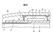
- 4C is an enlarged cross-sectional view of a portion surrounded by a broken line in FIG. 4B.
- FIG. 5A is a perspective view schematically showing the shielding unit and the substrate in FIGS. 4B and 4C.
- FIG. 5B is an exploded perspective view corresponding to FIG. 5A and shows a state where the cap of the shielding unit in FIG. 5A is removed from the frame.
- 5C is a cross-sectional view perpendicular to the horizontal direction of the shielding unit and the substrate in FIG. 5A.
- 6A is a cross-sectional view perpendicular to the front-rear direction of the shielding unit and the substrate in FIG.
- FIG. 5A shows a state before the device case is attached to the substrate.
- FIG. 6B is a cross-sectional view perpendicular to the front-rear direction of the shielding unit and the substrate in FIG. 5A and shows a state after the device case CS is attached to the substrate.
- FIG. 7A is an enlarged view showing the vicinity of the first side wall and the partition wall in FIG. 6A.
- FIG. 7B is an enlarged view showing the vicinity of the first side wall and the partition wall in FIG. 6B.
- FIG. 8A is an enlarged view similar to FIG. 7A and shows a shielding unit in which the partition wall is lower than the side wall of the frame due to manufacturing errors.
- FIG. 8B is an enlarged view similar to FIG.
- FIG. 7B shows the shielding unit in which the partition wall is lower than the side wall of the frame due to manufacturing errors.
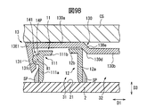
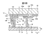
- FIG. 9A is an enlarged view similar to FIG. 7A and shows a first modification of the cap of the shielding unit.
- FIG. 9B is an enlarged view similar to FIG. 7B and shows a first modification of the cap of the shielding unit.
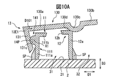
- FIG. 10A is an enlarged view similar to FIG. 7A and shows a second modification of the cap of the shielding unit.
- FIG. 10B is an enlarged view similar to FIG. 7B and shows a second modification of the cap of the shielding unit.
- a wireless communication device such as a mobile phone or a smartphone is illustrated as an electronic device including a surface-mount type shielding unit.
- the electronic device including the surface mount type shielding unit may be another device having a wireless communication function such as a tablet terminal or a mobile PC.
- FIG. 4A is an exploded perspective view of an electronic device ED including a surface mount type shielding unit 1 according to an embodiment of the present application.
- the electronic device ED is a thin wireless communication device such as a mobile phone or a smartphone, and the shielding unit 1 is mounted on a substrate 2 disposed inside the device case CS of the electronic device ED.
- the electronic device ED includes a flat display unit DU, a device case CS attached to the back side of the display unit DU, and a substrate 2 disposed between the display unit DU and the device case CS. is doing.
- the electronic device ED includes a flat battery BT disposed between the display unit DU and the substrate 2.
- FIG. 4B is a cross-sectional view perpendicular to the longitudinal direction of the electronic device ED of FIG. 4A.
- the display unit DU includes a display panel DP such as an LCD panel that forms a display screen of the electronic device ED, and a display control unit DC such as an LCD controller located on the back surface of the display panel DP.
- the battery BT is a secondary battery such as a lithium ion battery or a nickel metal hydride battery.
- the device case CS has a convex curved cross section protruding in a direction away from the back surface of the display panel DP, and the edge of the device case CS in the horizontal direction is displayed on the display panel by a mounting member M having a predetermined shape. It is fixedly attached to the DP.
- An internal space for accommodating the display control unit DC, the battery BT, the substrate 2 and the shielding unit 1 is formed between the inner surface of the device case CS and the back surface of the display panel DP.
- the substrate 2 is a flat plate member for fixing and wiring various electronic components.
- the board 2 is, for example, a printed board.
- the electronic device ED includes a plurality of electronic components EC1 and EC2 mounted on the upper surface 21 of the substrate 2 facing the inner surface of the device case CS.
- the shielding unit 1 is mounted on the upper surface 21 of the substrate 2 by the soldering part SP so as to cover the plurality of electronic components EC1 and EC2 together. That is, the shielding unit 1 plays a role of shielding electromagnetic noise radiated from the plurality of electronic components EC1 and EC2 on the substrate 2.
- 4C is an enlarged cross-sectional view of a portion surrounded by a broken line in FIG. 4B. As shown in FIG.
- the electronic device ED includes a substrate holding member H attached to the lower surface 22 of the substrate 2 so as to support the substrate 2, and the substrate holding member H is formed by laminating two thin plates. Is formed by.
- the substrate holding member H is fixed to the mounting member M via a fixing member F having a predetermined shape (see FIG. 4B). That is, the device case CS is attached to the substrate 2 via the attachment member M, the fixing member F, and the substrate holding member H.
- the shielding unit 1 includes a frame 11 that is mounted on the upper surface 21 of the substrate 2 so as to surround the plurality of electronic components EC1 and EC2, and a frame that partitions the space inside the frame 11. 11 and the partition wall 12 attached to 11. Furthermore, the shielding unit 1 has a cap 13 attached to the frame 11 so as to cover the upper part of the frame 11.
- the frame 11, the partition wall 12, and the cap 13 of the shielding unit 1 are made of various conductive materials that block electromagnetic waves, and are made of, for example, metal materials such as copper, aluminum, and brass. The structure of each part of the shielding unit 1 will be described with reference to FIGS. 5A to 5C and the like.
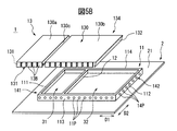
- FIG. 5A is a perspective view schematically showing the substrate 2 and the shielding unit 1 in FIGS. 4A to 4C
- FIG. 5B is an exploded perspective view corresponding to FIG. 5A, and shows the shielding unit 1 in FIG. 5A.
- a state where the cap 13 is removed from the frame 11 is shown.
- illustration of a plurality of electronic components EC1 and EC2 mounted on the substrate 2 is omitted.
- the frame 11 of the shielding unit 1 includes a first side wall 111 and a second side wall 112 that extend parallel to each other along the upper surface 21 of the substrate 2, and a first side wall 111 and a second side wall 112.
- the direction in which the two side walls 111 and 112 are arranged is referred to as the left-right direction
- the direction in which the front wall 113 and the rear wall 114 are arranged is referred to as the front-rear direction.
- the left-right direction is represented by an arrow D1
- the front-rear direction is represented by an arrow D2 (the same applies to other drawings).
- the partition wall 12 of the shielding unit 1 is located between the first and second side walls 111 and 112 and extends in parallel with the first and second side walls 111 and 112.
- the internal space of the frame 11 located between the first side wall 111 and the partition wall 12 is referred to as a first internal space 31, and the frame located between the second side wall 112 and the partition wall 12 is referred to as the first internal space 31.
- the internal space is referred to as a second internal space 32.
- the first electronic component EC1 is disposed in the first internal space 31 of the frame 11, and the second electronic component EC2 is disposed in the second internal space 32 (see FIG. 4B).
- the first electronic component EC1 is a CPU
- the second electronic component EC2 is a wireless component.
- the partition wall 12 plays a role of preventing noise leakage between the first and second inner spaces 31, 32 of the frame 11, and thereby noise interference between the first and second electronic components EC1, EC2. Yes.
- the cap 13 of the shielding unit 1 includes a top plate 130 that covers the first and second internal spaces 31 and 32 of the frame 11.
- the cap 13 of the shielding unit 1 includes a first side plate 131 that faces the outer surface of the first side wall 111 of the frame 11, a second side plate 132 that faces the outer surface of the second side wall 112 of the frame 11, and Contains.
- the top plate 130 of the cap 13 includes a first plate-like portion 130a adjacent to the first side plate 131, and a second plate-like portion 130b adjacent to the second side plate 132. And a recessed portion 130c positioned between the two plate-like portions 130a and 130b.
- the recessed portion 130 c of the top plate 130 is recessed in a direction away from the inner surfaces of the plate-like portions 130 a and 130 b facing the upper surface 21 of the substrate 2 (that is, toward the upper surface 21 of the substrate 2).
- the inner space 32 extends in the front-rear direction along the partition wall 12.
- the recessed part 130c of the top plate 130 in FIGS. 5A and 5B has a V-shaped cross section in a plane perpendicular to the front-rear direction.
- the recessed portion 130 c of the top plate 130 has an inclined surface that can slide-contact with the upper end portion of the partition wall 12. This inclined surface will be further described later with reference to FIGS. 6A and 6B.
- the first side wall 111 of the frame 11 has a first support portion 141 that supports the first side plate 131 of the cap 13.
- the second side wall 112 of the frame 11 has a second support portion 142 that supports the second side plate 132 of the cap 13.
- the second support portion 142 is formed of a plurality of protrusions 14 ⁇ / b> P that protrude from the outer surface of the second side wall 112.
- the first support portion 141 is formed from a plurality of protrusions 14 ⁇ / b> P that protrude from the outer surface of the first side wall 111.
- the detailed structure of the two support portions 141 and 142 will be described later with reference to FIGS. 7A and 7B.
- the cap 13 further includes a front surface portion 133 that faces the outer surface of the front wall 113 of the frame 11 and a rear surface portion 134 that faces the outer surface of the rear wall 114 of the frame 11. .
- the front surface portion 133 of the cap 13 is formed of a plurality of plate-like portions 13B arranged at intervals in the left-right direction.
- the rear surface portion 134 of the cap 13 is formed of a plurality of plate-like portions 13B arranged at intervals in the left-right direction.
- the plate-like portion 13B is a small thin plate and is formed integrally with the top plate 130. As shown in FIG.
- the outer surface of the front wall 113 of the frame 11 is provided with a plurality of protrusions 11P that are spaced apart in the left-right direction.
- a plurality of protrusions 11P are provided on the outer surface of the rear wall 114 of the frame 11 so as to be spaced apart in the left-right direction.
- Each plate-like portion 13B of the front surface portion 133 is provided with a recess that engages with the protrusion 11P of the front wall 113.
- each plate-like portion 13B of the rear surface portion 134 is provided with a recess that engages with the protrusion 11P of the rear wall 114.
- the structure of each plate-like part 13B of the front part 133 and the rear part 134 will be described with reference to FIG. 5C.
- FIG. 5C is a cross-sectional view perpendicular to the left-right direction of the shielding unit 1 and the substrate 2 in FIG. 5A.
- the front wall 113 of the frame 11 has a partially spherical protrusion 11P.
- the plate-like portion 13B of the front surface portion 133 of the cap 13 has a partial spherical concave surface 13C that can accommodate the protrusion 11P of the front wall 113 of the frame 11.
- the concave surface 13C of the plate-like portion 13B of the front surface portion 133 has a larger diameter than the protrusion 11P of the front wall 113.
- the individual plate-like portions 13B of the front surface portion 133 are movable within a predetermined range in the vertical direction with respect to the front wall 113 of the frame 11.
- the up-down direction here is a direction perpendicular to both the left-right direction and the front-rear direction.
- the above vertical direction is indicated by an arrow D3 (the same applies to other drawings).
- the concave surface 13C of the plate-like portion 13B of the rear surface portion 134 has a larger diameter than the protrusion 11P of the rear wall 114 (see FIGS. 5A and 5B). Therefore, each plate-like portion 13B of the rear surface portion 134 is movable within a predetermined range in the vertical direction with respect to the rear wall 114 of the frame 11.
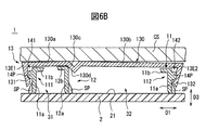
- FIG. 6A and 6B are cross-sectional views perpendicular to the front-rear direction of the shielding unit 1 and the substrate 2 in FIG. 5A.
- 6A shows a state before the device case CS is attached to the substrate 2
- FIG. 6B shows a state after the device case CS is attached to the substrate 2 (FIGS. 4A to 4). See also FIG. 4C).
- 6A and 6B, the first side wall 111, the second side wall 112, and the partition wall 12 of the frame 11 are fixed to the upper surface 21 of the substrate 2 by the soldering portion SP.
- Each of the side walls 111 and 112 is provided with a main body portion 11a erected perpendicularly to the upper surface 21 of the substrate 2 and a horizontal line extending from the upper end portion of the main body portion 11a in parallel to the upper surface 21 of the substrate 2 and toward the partition wall 12. Part 11b.
- the partition wall 12 includes a main body portion 12a erected perpendicularly to the upper surface 21 of the substrate 2, and an upper end portion of the main body portion 12a parallel to the upper surface 21 of the substrate 2 and And a horizontal portion 12b extending toward one side wall 111.
- the main body 12a of the partition wall 12 is designed to have a predetermined height that does not cause the top plate 130 to lift. Said predetermined height is the same height as the main-body part 11a of each side wall 111,112 of the flame
- the actual partition wall 12 may be higher or lower than the side walls 111 and 112 of the frame 11 due to manufacturing errors and the like. In the example of FIGS.
- the partition wall 12 is higher than the side walls 111 and 112 of the frame 11. Therefore, in the state of FIG. 6A, a part of the top plate 130 is lifted by the partition wall 12. However, the lifting of the top plate 130 is eliminated by, for example, receiving a downward pressing force acting on the top plate 130 when the apparatus case CS is attached, and moving each part of the cap 13 relative to the frame 11 and the partition wall 12. (See FIG. 6B). The behavior of the cap 13 for eliminating the lifting of the top plate 130 will be described later.
- the first side plate 131 of the cap 13 forms an acute angle with respect to the first plate-like portion 130a of the top plate 130.
- the second side plate 132 forms an acute angle with respect to the second plate-like portion 130 b of the top plate 130.
- the surface of the recessed portion 130 c facing the substrate 2 includes an inclined surface 130 d that can slide-contact with the upper end portion of the main body 12 a of the partition wall 12.
- An inclined surface 130d of the cap 13 in FIGS. 6A and 6B is a flat surface formed so as to be inclined with respect to the upper surface 21 of the substrate 2, and forms an obtuse angle with the adjacent first plate-like portion 130a. . As shown in FIGS.
- the inclined surface 130 d of the cap 13 is in contact with the upper end portion of the partition wall 12 in both the state before and after the device case CS is attached to the substrate 2. Therefore, according to the cap 13 in FIGS. 6A and 6B, noise leakage between the first and second inner spaces 31 and 32 of the frame 11, and thereby between the first and second electronic components EC ⁇ b> 1 and EC ⁇ b> 2. Noise interference can be effectively prevented. Further, the cap 13 is formed such that the inclined surface 130d slides obliquely downward with respect to the upper end portion of the partition wall 12 as the top plate 130 is pressed downward by the device case CS or the like. The inclined surface 130d in FIGS.
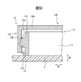
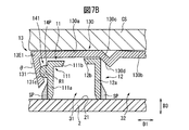
- FIG. 7A is an enlarged view showing the vicinity of the first side wall 111 and the partition wall 12 in FIG. 6A.
- 7B is an enlarged view showing the vicinity of the first side wall 111 and the partition wall 12 in FIG. 6B.
- the first support portion 141 is configured so that the outer edge portion 13E1 of the top plate 130 adjacent to the first side plate 131 (that is, the outer edge portion 13E1 of the first plate-like portion 130a) can move in the direction toward the partition wall 12. 1 side plate 131 is supported.
- the second support portion 142 can move in a direction in which the outer edge portion 13E2 of the top plate 130 adjacent to the second side plate 132 (that is, the outer edge portion 13E2 of the second plate-like portion 130b) is separated from the partition wall 12.
- the second side plate 132 is supported (see FIGS. 6A and 6B).
- the first support part 141 includes a plurality of partial spherical protrusions 14P protruding from the outer surface of the first side wall 111, and the plurality of protrusions 14P are parallel to the front-rear direction and It arrange
- a plurality of partial spherical concave surfaces 131 ⁇ / b> C that engage with the plurality of protrusions 14 ⁇ / b> P of the first support portion 141 are provided on the inner surface of the first side plate 131 that faces the first side wall 111.
- the plurality of concave surfaces 131 ⁇ / b> C of the first side plate 131 are formed so as to be in sliding contact with the plurality of protrusions 14 ⁇ / b> P of the first support portion 141.
- the entire first side plate 131 is moved as the plurality of concave surfaces 131C slide relative to the plurality of protrusions 14P. Oscillates around the support shaft R1 along the direction in which the plurality of protrusions 14P are arranged.
- the support shaft R1 extends in parallel with the front-rear direction. That is, the support shaft R1 extends perpendicular to the paper surface of FIGS. 7A and 7B.
- the magnitude of the angle ⁇ formed between the first side plate 131 and the vertical plane changes, so that the outer edge portion 13E1 of the top plate 130 is It moves in the direction toward the partition wall 12 or in the direction away from the partition wall 12.
- the angle ⁇ formed becomes smaller, so that the outer edge portion 13E1 of the top plate 130 becomes the partition wall 12. (See arrow D72 in FIG. 7A).
- the behavior of the cap 13 for eliminating the above-described lifting of the top plate 130 will be described with reference to FIGS. 6A and 6B again.
- the inclined surface 130 d slides obliquely downward with respect to the partition wall 12 as the raised portion of the top plate 130 is pressed downward by the device case CS.
- the cap 13 is formed such that the first outer edge portion 13E1 of the top plate 130 moves toward the partition wall 12 in conjunction with the slanting surface 130d sliding obliquely downward with respect to the partition wall 12.
- the moving direction of the first outer edge portion 13E1 is indicated by an arrow D61 in FIG. 6A.
- the cap 13 is formed such that the second outer edge portion 13E2 of the top plate 130 moves in a direction away from the partition wall 12 in conjunction with the inclined surface 130d sliding obliquely downward with respect to the partition wall 12.
- the moving direction of the second outer edge portion 13E2 is represented by an arrow D62 in FIG. 6A.
- the inclined surface 130d can be slid obliquely downward by the downward pressing force acting on the top plate 130 of the cap 13 from the device case CS when the device case CS is attached. As a result, there is no need to provide a clearance for preventing the contact between the top plate 130 of the cap 13 and the device case CS, so that the electronic device ED can be thinned.
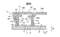
- FIGS. 8A and 8B are enlarged views similar to FIGS. 7A and 7B.
- the partition wall 12 is higher than the first side wall 111 of the frame 11 due to a manufacturing error of the partition wall 12.
- the partition wall 12 is lower than the first side wall 111 of the frame 11 due to a manufacturing error of the partition wall 12.
- the inclined surface 130 d of the cap 13 is in contact with the upper end portion of the partition wall 12 in both the state before and after the device case CS is attached to the substrate 2. Therefore, also in the example of FIGS. 8A and 8B, noise leakage between the first and second inner spaces 31 and 32 of the frame 11 and noise interference caused thereby can be effectively prevented.
- the inclined surface 130d of the cap 13 is formed so as to always contact the upper end of the partition wall 12 even when the dimensions of the partition wall 12 vary. Further, the inclined surface 130d of the cap 13 is formed so as to always come into contact with the upper end portion of the partition wall 12 even when the mounting position in the left-right direction of the partition wall 12 varies. That is, the position and dimensions of the inclined surface 130d in the cap 13 ensure that the inclined surface 130d contacts the upper end of the partition wall 12 as long as the manufacturing error of the partition wall 12 is within a predetermined tolerance range. Has been determined to be. Thereby, the partition wall 12 can exhibit a desired shielding performance inside the frame 11. 8A and 8B, since the partition wall 12 does not lift a part of the top plate 130 of the cap 13, the top plate 130 is pressed downward by the device case CS when the device case CS is attached. There is nothing.
- the top plate 130 of the cap 13 of this example includes a plate-like inclined portion 130 e that forms the above-described inclined surface 130 d capable of sliding contact with the upper end portion of the partition wall 12.
- the top plate 130 of the cap 13 of this example includes a first plate-like portion 130a extending from the upper edge of the inclined portion 130e to the first side plate 131, and a second edge from the lower edge of the inclined portion 130e.
- a second plate portion 130b extending to the side plate 132 (not shown in FIGS. 9A and 9B). That is, a stepped portion formed by the inclined portion 130e exists between the first plate-like portion 130a and the second plate-like portion 130b. As shown in FIGS. 9A and 9B, the inclined portion 130e forms an obtuse angle with each of the first plate-like portion 130a and the second plate-like portion 130b.
- the structure of the portion other than the top plate 130 of the cap 13 in FIGS. 9A and 9B is the same as the example in FIGS. 7A and 7B. Moreover, the structure of the frame 11 and the partition wall 12 in FIGS. 9A and 9B is the same as the example of FIGS. 7A and 7B. That is, in the cap 13 of this example, the outer edge portion 13E1 of the first plate-like portion 130a faces the partition wall 12 in conjunction with the inclined surface 130d sliding obliquely downward with respect to the upper end portion of the partition wall 12. It is formed to move.
- the moving direction of the outer edge portion 13E1 is represented by an arrow D91 in the drawing. As shown in FIG.
- the distance from the upper surface 21 of the substrate 2 to the top plate 130 is changed between the first plate-like portion 130a and the second plate-like portion 130b. Can do. Therefore, according to the cap 13 of this example, it is possible to dispose two electronic components having greatly different height dimensions in the first and second internal spaces 31 and 32 of the frame 11.
- the top plate 130 of the cap 13 of this example includes a first plate-like portion 130a adjacent to the first side plate 131 and a second side plate 132 (omitted in FIGS. 10A and 10B). ) Adjacent to the second plate-like portion 130b.
- the top plate 130 of the cap 13 of this example has a recessed portion 130c located between the first and second plate-like portions 130a and 130b.
- the recessed part 130c of the cap 13 of this example is in a direction away from the inner surfaces of the first and second plate-like parts 130a and 130b (that is, the upper surface of the substrate 2), like the recessed part 130c in FIGS. 7 and 7B. It is depressed (toward 21).
- the recessed portion 130c in FIGS. 7A and 7B has a V-shaped cross section in a plane perpendicular to the front-rear direction, whereas the recessed portion 130c of the cap 13 of this example faces downward in the same plane. It has a convex curved cross section.
- FIGS. 10A and the structure of the portion other than the top plate 130 of the cap 13 in FIG. 10 is the same as the example of FIGS. 7A and 7B.
- the structures of the frame 11 and the partition wall 12 in FIGS. 10A and 10B are the same as those in the examples of FIGS. 7A and 7B. That is, in the cap 13 of this example, the outer edge portion 13E1 of the first plate-like portion 130a faces the partition wall 12 in conjunction with the inclined surface 130d sliding obliquely downward with respect to the upper end portion of the partition wall 12. It is formed to move.
- the moving direction of the outer edge portion 13E1 is represented by an arrow D101 in the drawing.
- the top plate can be formed by sliding the inclined surface 130d obliquely downward with respect to the partition wall 12.
- the lifting of 130 can be eliminated. As a result, it is not necessary to provide a clearance for preventing contact between the cap 13 and the device case CS, so that the electronic device ED can be thinned.
- the present invention is not limited to the above-described embodiment, and can be variously modified within the scope described in the claims.
- the dimensions, shapes, materials, and the like of the respective portions of the shielding unit described above are merely examples, and various sizes, shapes, materials, and the like can be employed to achieve the effects of the present invention.
Landscapes
- Engineering & Computer Science (AREA)
- Microelectronics & Electronic Packaging (AREA)
- Shielding Devices Or Components To Electric Or Magnetic Fields (AREA)
- Casings For Electric Apparatus (AREA)
Abstract
L'invention concerne une unité de protection (1) pouvant être montée sur une surface comprenant : un cadre (11) qui entoure une multiplicité de composants électroniques montés sur un substrat (2) ; une paroi de séparation (12) qui sépare un espace à l'intérieur de (11) l'endroit où les composants électroniques sont situés ; et un capuchon (13) qui comprend une plaque supérieure (130) recouvrant le cadre (11), des plaques latérales (131, 132) faisant face aux surfaces externes du cadre (11) et une surface diagonale (130d) formée dans un emplacement sur la surface interne de la plaque supérieure (130), faisant face à la paroi de séparation (12), de manière à pouvoir établir un contact coulissant avec la paroi de séparation (12). Le cadre (11) présente des sections de support (141, 142) qui supportent les plaques latérales (131, 132), de sorte que les sections de bord externes (13E1, 13E2) de (130), qui sont adjacentes aux plaques latérales (131, 132), puissent se déplacer dans la direction vers la paroi de séparation (12) ou dans la direction s'éloignant de la paroi de séparation (12). Le capuchon (13) est formé de sorte que les sections de bord externes (13E1, 13E2) se déplacent dans la direction vers la paroi de séparation (12) ou s'éloignant de la paroi de séparation (12) en conjonction avec le mouvement coulissant de la surface diagonale (130d) qui est un mouvement en diagonale vers le bas par rapport à la paroi de séparation (12).
Priority Applications (2)
| Application Number | Priority Date | Filing Date | Title |
|---|---|---|---|
| PCT/JP2015/063927 WO2016181553A1 (fr) | 2015-05-14 | 2015-05-14 | Unité de protection pouvant être montée sur une surface et dispositif électronique la comprenant |
| JP2017517567A JP6439221B2 (ja) | 2015-05-14 | 2015-05-14 | 表面実装型の遮蔽ユニット及び遮蔽ユニットを備える電子機器 |
Applications Claiming Priority (1)
| Application Number | Priority Date | Filing Date | Title |
|---|---|---|---|
| PCT/JP2015/063927 WO2016181553A1 (fr) | 2015-05-14 | 2015-05-14 | Unité de protection pouvant être montée sur une surface et dispositif électronique la comprenant |
Publications (1)
| Publication Number | Publication Date |
|---|---|
| WO2016181553A1 true WO2016181553A1 (fr) | 2016-11-17 |
Family
ID=57249508
Family Applications (1)
| Application Number | Title | Priority Date | Filing Date |
|---|---|---|---|
| PCT/JP2015/063927 Ceased WO2016181553A1 (fr) | 2015-05-14 | 2015-05-14 | Unité de protection pouvant être montée sur une surface et dispositif électronique la comprenant |
Country Status (2)
| Country | Link |
|---|---|
| JP (1) | JP6439221B2 (fr) |
| WO (1) | WO2016181553A1 (fr) |
Cited By (2)
| Publication number | Priority date | Publication date | Assignee | Title |
|---|---|---|---|---|
| WO2019164190A1 (fr) * | 2018-02-21 | 2019-08-29 | 삼성전자 주식회사 | Dispositif électronique comportant une structure de boîtier de blindage |
| CN116190250A (zh) * | 2023-02-09 | 2023-05-30 | 青岛歌尔微电子研究院有限公司 | 电子设备的封装方法和封装结构 |
Citations (5)
| Publication number | Priority date | Publication date | Assignee | Title |
|---|---|---|---|---|
| JPS59158594A (ja) * | 1983-02-28 | 1984-09-08 | 株式会社村田製作所 | 高周波機器のシ−ルドケ−ス |
| JPS59151497U (ja) * | 1983-03-29 | 1984-10-11 | 日本電気ホームエレクトロニクス株式会社 | シ−ルド仕切板 |
| JPS63156399A (ja) * | 1986-12-19 | 1988-06-29 | 松下電器産業株式会社 | シ−ルド装置 |
| JP2003188572A (ja) * | 2001-12-20 | 2003-07-04 | Sharp Corp | 電子チューナ |
| JP2014225515A (ja) * | 2013-05-15 | 2014-12-04 | 富士通株式会社 | シールドケースおよび電子機器 |
-
2015
- 2015-05-14 JP JP2017517567A patent/JP6439221B2/ja not_active Expired - Fee Related
- 2015-05-14 WO PCT/JP2015/063927 patent/WO2016181553A1/fr not_active Ceased
Patent Citations (5)
| Publication number | Priority date | Publication date | Assignee | Title |
|---|---|---|---|---|
| JPS59158594A (ja) * | 1983-02-28 | 1984-09-08 | 株式会社村田製作所 | 高周波機器のシ−ルドケ−ス |
| JPS59151497U (ja) * | 1983-03-29 | 1984-10-11 | 日本電気ホームエレクトロニクス株式会社 | シ−ルド仕切板 |
| JPS63156399A (ja) * | 1986-12-19 | 1988-06-29 | 松下電器産業株式会社 | シ−ルド装置 |
| JP2003188572A (ja) * | 2001-12-20 | 2003-07-04 | Sharp Corp | 電子チューナ |
| JP2014225515A (ja) * | 2013-05-15 | 2014-12-04 | 富士通株式会社 | シールドケースおよび電子機器 |
Cited By (5)
| Publication number | Priority date | Publication date | Assignee | Title |
|---|---|---|---|---|
| WO2019164190A1 (fr) * | 2018-02-21 | 2019-08-29 | 삼성전자 주식회사 | Dispositif électronique comportant une structure de boîtier de blindage |
| KR20190100744A (ko) * | 2018-02-21 | 2019-08-29 | 삼성전자주식회사 | 쉴드 캔 구조를 구비한 전자 장치 |
| US11076512B2 (en) | 2018-02-21 | 2021-07-27 | Samsung Electronics Co., Ltd. | Electronic device having shield can structure |
| KR102476599B1 (ko) | 2018-02-21 | 2022-12-12 | 삼성전자주식회사 | 쉴드 캔 구조를 구비한 전자 장치 |
| CN116190250A (zh) * | 2023-02-09 | 2023-05-30 | 青岛歌尔微电子研究院有限公司 | 电子设备的封装方法和封装结构 |
Also Published As
| Publication number | Publication date |
|---|---|
| JPWO2016181553A1 (ja) | 2017-12-07 |
| JP6439221B2 (ja) | 2018-12-19 |
Similar Documents
| Publication | Publication Date | Title |
|---|---|---|
| EP3340006B1 (fr) | Ensemble boîtier, module de caméra double et terminal mobile | |
| JP5233677B2 (ja) | 電子機器のシールド構造、シールド部材及びこれを備える電子機器 | |
| US10306032B2 (en) | Bracket assembly, camera module, and mobile terminal | |
| JP3131870U (ja) | 電磁妨害遮蔽用のシールド装置 | |
| US9338934B2 (en) | Shield-can and jig for manufacturing shield-can | |
| CN106603776B (zh) | 终端 | |
| CN104811589A (zh) | 便携式电子装置及其相机模组 | |
| JP6439221B2 (ja) | 表面実装型の遮蔽ユニット及び遮蔽ユニットを備える電子機器 | |
| JPWO2012176646A1 (ja) | シールドフレーム、シールドフレームの実装構造、及び電子携帯機器 | |
| JP2014170830A (ja) | 電磁波の遮蔽構造、これを備えた電子機器及び電磁波の遮蔽方法 | |
| CN104811590A (zh) | 便携式电子装置及其相机模组 | |
| JP5224407B2 (ja) | シールドケースおよび電子機器 | |
| US20110192626A1 (en) | Apparatus with case | |
| JP2013254925A (ja) | 電子回路装置 | |
| JP6508403B1 (ja) | 電子機器の筐体および電子機器 | |
| JP6006025B2 (ja) | 制御ユニット | |
| JP2009168987A (ja) | 回路基板モジュール及び電子機器 | |
| JP2019096646A (ja) | 電子機器 | |
| US9788467B2 (en) | Shield case | |
| JP2017157656A (ja) | 電子機器の筐体構造 | |
| WO2017202050A1 (fr) | Cadre, ensemble boîtier et terminal | |
| JPWO2014109032A1 (ja) | 電子機器 | |
| CN223219385U (zh) | 屏蔽组件及电子设备 | |
| US10903564B2 (en) | Communication apparatus | |
| CN206611454U (zh) | 手机 |
Legal Events
| Date | Code | Title | Description |
|---|---|---|---|
| 121 | Ep: the epo has been informed by wipo that ep was designated in this application |
Ref document number: 15891877 Country of ref document: EP Kind code of ref document: A1 |
|
| ENP | Entry into the national phase |
Ref document number: 2017517567 Country of ref document: JP Kind code of ref document: A |
|
| NENP | Non-entry into the national phase |
Ref country code: DE |
|
| 122 | Ep: pct application non-entry in european phase |
Ref document number: 15891877 Country of ref document: EP Kind code of ref document: A1 |