WO2016181838A1 - Dispositif d'éclairage, dispositif d'affichage, et récepteur de télévision - Google Patents
Dispositif d'éclairage, dispositif d'affichage, et récepteur de télévision Download PDFInfo
- Publication number
- WO2016181838A1 WO2016181838A1 PCT/JP2016/063179 JP2016063179W WO2016181838A1 WO 2016181838 A1 WO2016181838 A1 WO 2016181838A1 JP 2016063179 W JP2016063179 W JP 2016063179W WO 2016181838 A1 WO2016181838 A1 WO 2016181838A1
- Authority
- WO
- WIPO (PCT)
- Prior art keywords
- light
- guide plate
- incident surface
- light incident
- edge
- Prior art date
- Legal status (The legal status is an assumption and is not a legal conclusion. Google has not performed a legal analysis and makes no representation as to the accuracy of the status listed.)
- Ceased
Links
Images





Classifications
-
- G—PHYSICS
- G02—OPTICS
- G02F—OPTICAL DEVICES OR ARRANGEMENTS FOR THE CONTROL OF LIGHT BY MODIFICATION OF THE OPTICAL PROPERTIES OF THE MEDIA OF THE ELEMENTS INVOLVED THEREIN; NON-LINEAR OPTICS; FREQUENCY-CHANGING OF LIGHT; OPTICAL LOGIC ELEMENTS; OPTICAL ANALOGUE/DIGITAL CONVERTERS
- G02F1/00—Devices or arrangements for the control of the intensity, colour, phase, polarisation or direction of light arriving from an independent light source, e.g. switching, gating or modulating; Non-linear optics
- G02F1/01—Devices or arrangements for the control of the intensity, colour, phase, polarisation or direction of light arriving from an independent light source, e.g. switching, gating or modulating; Non-linear optics for the control of the intensity, phase, polarisation or colour
- G02F1/13—Devices or arrangements for the control of the intensity, colour, phase, polarisation or direction of light arriving from an independent light source, e.g. switching, gating or modulating; Non-linear optics for the control of the intensity, phase, polarisation or colour based on liquid crystals, e.g. single liquid crystal display cells
- G02F1/133—Constructional arrangements; Operation of liquid crystal cells; Circuit arrangements
- G02F1/1333—Constructional arrangements; Manufacturing methods
- G02F1/1335—Structural association of cells with optical devices, e.g. polarisers or reflectors
- G02F1/1336—Illuminating devices
- G02F1/133615—Edge-illuminating devices, i.e. illuminating from the side
-
- G—PHYSICS
- G02—OPTICS
- G02B—OPTICAL ELEMENTS, SYSTEMS OR APPARATUS
- G02B6/00—Light guides; Structural details of arrangements comprising light guides and other optical elements, e.g. couplings
- G02B6/0001—Light guides; Structural details of arrangements comprising light guides and other optical elements, e.g. couplings specially adapted for lighting devices or systems
- G02B6/0011—Light guides; Structural details of arrangements comprising light guides and other optical elements, e.g. couplings specially adapted for lighting devices or systems the light guides being planar or of plate-like form
- G02B6/0081—Mechanical or electrical aspects of the light guide and light source in the lighting device peculiar to the adaptation to planar light guides, e.g. concerning packaging
- G02B6/0085—Means for removing heat created by the light source from the package
-
- G—PHYSICS
- G02—OPTICS
- G02F—OPTICAL DEVICES OR ARRANGEMENTS FOR THE CONTROL OF LIGHT BY MODIFICATION OF THE OPTICAL PROPERTIES OF THE MEDIA OF THE ELEMENTS INVOLVED THEREIN; NON-LINEAR OPTICS; FREQUENCY-CHANGING OF LIGHT; OPTICAL LOGIC ELEMENTS; OPTICAL ANALOGUE/DIGITAL CONVERTERS
- G02F1/00—Devices or arrangements for the control of the intensity, colour, phase, polarisation or direction of light arriving from an independent light source, e.g. switching, gating or modulating; Non-linear optics
- G02F1/01—Devices or arrangements for the control of the intensity, colour, phase, polarisation or direction of light arriving from an independent light source, e.g. switching, gating or modulating; Non-linear optics for the control of the intensity, phase, polarisation or colour
- G02F1/13—Devices or arrangements for the control of the intensity, colour, phase, polarisation or direction of light arriving from an independent light source, e.g. switching, gating or modulating; Non-linear optics for the control of the intensity, phase, polarisation or colour based on liquid crystals, e.g. single liquid crystal display cells
- G02F1/133—Constructional arrangements; Operation of liquid crystal cells; Circuit arrangements
- G02F1/1333—Constructional arrangements; Manufacturing methods
- G02F1/1335—Structural association of cells with optical devices, e.g. polarisers or reflectors
- G02F1/133553—Reflecting elements
-
- G—PHYSICS
- G02—OPTICS
- G02B—OPTICAL ELEMENTS, SYSTEMS OR APPARATUS
- G02B6/00—Light guides; Structural details of arrangements comprising light guides and other optical elements, e.g. couplings
- G02B6/0001—Light guides; Structural details of arrangements comprising light guides and other optical elements, e.g. couplings specially adapted for lighting devices or systems
- G02B6/0011—Light guides; Structural details of arrangements comprising light guides and other optical elements, e.g. couplings specially adapted for lighting devices or systems the light guides being planar or of plate-like form
- G02B6/0013—Means for improving the coupling-in of light from the light source into the light guide
- G02B6/0023—Means for improving the coupling-in of light from the light source into the light guide provided by one optical element, or plurality thereof, placed between the light guide and the light source, or around the light source
- G02B6/0031—Reflecting element, sheet or layer
-
- G—PHYSICS
- G02—OPTICS
- G02B—OPTICAL ELEMENTS, SYSTEMS OR APPARATUS
- G02B6/00—Light guides; Structural details of arrangements comprising light guides and other optical elements, e.g. couplings
- G02B6/0001—Light guides; Structural details of arrangements comprising light guides and other optical elements, e.g. couplings specially adapted for lighting devices or systems
- G02B6/0011—Light guides; Structural details of arrangements comprising light guides and other optical elements, e.g. couplings specially adapted for lighting devices or systems the light guides being planar or of plate-like form
- G02B6/0066—Light guides; Structural details of arrangements comprising light guides and other optical elements, e.g. couplings specially adapted for lighting devices or systems the light guides being planar or of plate-like form characterised by the light source being coupled to the light guide
- G02B6/0068—Arrangements of plural sources, e.g. multi-colour light sources
-
- G—PHYSICS
- G02—OPTICS
- G02B—OPTICAL ELEMENTS, SYSTEMS OR APPARATUS
- G02B6/00—Light guides; Structural details of arrangements comprising light guides and other optical elements, e.g. couplings
- G02B6/0001—Light guides; Structural details of arrangements comprising light guides and other optical elements, e.g. couplings specially adapted for lighting devices or systems
- G02B6/0011—Light guides; Structural details of arrangements comprising light guides and other optical elements, e.g. couplings specially adapted for lighting devices or systems the light guides being planar or of plate-like form
- G02B6/0066—Light guides; Structural details of arrangements comprising light guides and other optical elements, e.g. couplings specially adapted for lighting devices or systems the light guides being planar or of plate-like form characterised by the light source being coupled to the light guide
- G02B6/0073—Light emitting diode [LED]
-
- G—PHYSICS
- G02—OPTICS
- G02B—OPTICAL ELEMENTS, SYSTEMS OR APPARATUS
- G02B6/00—Light guides; Structural details of arrangements comprising light guides and other optical elements, e.g. couplings
- G02B6/0001—Light guides; Structural details of arrangements comprising light guides and other optical elements, e.g. couplings specially adapted for lighting devices or systems
- G02B6/0011—Light guides; Structural details of arrangements comprising light guides and other optical elements, e.g. couplings specially adapted for lighting devices or systems the light guides being planar or of plate-like form
- G02B6/0081—Mechanical or electrical aspects of the light guide and light source in the lighting device peculiar to the adaptation to planar light guides, e.g. concerning packaging
- G02B6/0086—Positioning aspects
- G02B6/0088—Positioning aspects of the light guide or other optical sheets in the package
-
- G—PHYSICS
- G02—OPTICS
- G02B—OPTICAL ELEMENTS, SYSTEMS OR APPARATUS
- G02B6/00—Light guides; Structural details of arrangements comprising light guides and other optical elements, e.g. couplings
- G02B6/0001—Light guides; Structural details of arrangements comprising light guides and other optical elements, e.g. couplings specially adapted for lighting devices or systems
- G02B6/0011—Light guides; Structural details of arrangements comprising light guides and other optical elements, e.g. couplings specially adapted for lighting devices or systems the light guides being planar or of plate-like form
- G02B6/0081—Mechanical or electrical aspects of the light guide and light source in the lighting device peculiar to the adaptation to planar light guides, e.g. concerning packaging
- G02B6/0086—Positioning aspects
- G02B6/009—Positioning aspects of the light source in the package
Definitions
- the present invention relates to a lighting device, a display device, and a television receiver.
- a liquid crystal display device such as a liquid crystal television requires a backlight device as a separate illumination device because the liquid crystal panel that is the display panel does not emit light.
- Backlight devices are roughly classified into direct type and edge light type according to the mechanism, and it is preferable to use an edge light type backlight device in order to realize further thinning of the liquid crystal display device. ing.
- a light guide plate having a light incident surface provided on at least one end surface and a light emitting surface on one plate surface, and a plurality of light sources such as LEDs (Light Emitting Diodes) on the mounting surface A light source substrate, etc., which is mounted and disposed so that the mounting surface faces the light emitting surface of the light guide plate, is accommodated in the housing.
- LEDs Light Emitting Diodes
- a light source substrate, etc. which is mounted and disposed so that the mounting surface faces the light emitting surface of the light guide plate, is accommodated in the housing.
- brightness unevenness may occur in the light emitted from the light exit surface of the light guide plate, and it is required to suppress such brightness unevenness.
- Patent Document 1 below discloses a planar illumination device that prevents luminance unevenness that occurs in the vicinity of a positioning protrusion provided on a light guide plate.
- the interval between the adjacent light sources between the adjacent light source substrates is the distance between each light source mounted on the mounting surface of the light source substrate. Larger than the interval. For this reason, when the edge on the light incident surface side of the light emitting surface of the light guide plate is viewed, a portion of the edge facing the adjacent light source substrate is displayed relatively darker than other portions. Sometimes. That is, a dark part may occur at the facing part. As a result, unevenness in brightness due to the dark portion may occur in the light emitted from the light exit surface of the light guide plate.
- the technology disclosed in this specification has been created in view of the above problems, and aims to suppress luminance unevenness.
- a light source and at least one end surface are a light incident surface on which light from the light source is incident, and one plate surface emits light incident from the light incident surface.
- a light guide plate having a light emitting surface and a mounting surface on which one of the light sources is mounted, and the mounting surface is arranged along the light incident surface so as to face the light incident surface.
- a plurality of light source substrates arranged in a manner of being opposed to a portion that has light reflectivity and faces between the adjacent light source substrates among the edges of the light emitting surface on the light incident surface side.
- a light reflecting member is arranged in a manner of being opposed to a portion that has light reflectivity and faces between the adjacent light source substrates among the edges of the light emitting surface on the light incident surface side.
- the interval between adjacent light sources is larger than the interval between the light sources mounted on the mounting surface of the light source substrate. Therefore, a dark part occurs in a portion of the light emitting surface of the light guide surface on the light incident surface side that faces between adjacent light source substrates, and unevenness in luminance occurs in the light emitted from the light emitting surface. is there.
- the illumination device described above the light that has reached the light reflecting member out of the light emitted from the light emitting surface of the light guide plate is caused by the light reflecting member to end the light incident surface side of the light emitting surface of the light guide plate.
- the reflected light reaches the dark part generated in the facing part and the vicinity thereof, and the dark part can be eliminated. For this reason, it can suppress that the brightness nonuniformity resulting from the said dark part arises in the light radiate
- the illumination device may include a frame-shaped member having a cover portion that covers an edge of the light emitting surface, and the light reflecting member may be attached to a part of the cover portion.
- the optical sheet when the light reflecting member is disposed on the light emitting surface of the light guide plate, when the optical sheet or the like disposed on the light emitting surface undergoes thermal expansion, the optical sheet may interfere with the light reflecting member. is there. In said structure, interference with such a light reflection member and another member can be suppressed because a light reflection member is affixed on the cover part of a frame-shaped member.
- the illumination device may include a frame-like member having a cover portion that covers an edge of the light emitting surface, and the light reflecting member may be formed by painting a part of the cover portion in white.
- the thickness of the light reflecting member becomes equal to the thickness of the coating, for example, the thickness of the light reflecting member can be reduced as compared with the case where the light reflecting member is formed into a sheet shape. For this reason, thickness reduction of an illuminating device can be achieved.
- the light reflecting member may be disposed by being attached to a part of an edge of the light emitting surface on the light incident surface side.
- an optical sheet group composed of a plurality of optical sheets stacked on the light emitting surface is provided, and an edge on the light incident surface side of the optical sheet located on the upper layer side of the plurality of optical sheets
- a protrusion that protrudes toward the light source substrate may be provided, and the light reflecting member may be attached to the protrusion.
- the optical sheet when the light reflecting member is disposed on the light emitting surface of the light guide plate, when the optical sheet or the like disposed on the light emitting surface undergoes thermal expansion, the optical sheet may interfere with the light reflecting member. is there. In said structure, interference with such a light reflection member and another member can be suppressed because a light reflection member is affixed on the protrusion part of an optical sheet.
- a light source and at least one end surface is a light incident surface on which light from the light source is incident, and one plate surface receives light incident from the light incident surface.
- a light guide plate that is an emitted light exit surface, and one plate surface is a mounting surface on which a plurality of the light sources are mounted, and the mounting surface faces the light incident surface along the light incident surface.
- a plurality of light source substrates arranged side by side, and having a light scattering property, arranged so as to face a portion facing the adjacent light source substrate among the edges on the light incident surface side of the light emitting surface. And a light scattering member.
- the light that has reached the light scattering member among the light emitted from the light exit surface of the light guide plate is out of the edge on the light incident surface side of the light exit surface of the light guide plate by the light scattering member. Scattered to a portion facing between adjacent light source substrates.
- luminance of the dark part which arises in the said location and its vicinity is raised, and the difference of the brightness
- the illumination device includes an optical member including a plurality of optical sheets stacked on the light emission surface and imparting an optical function to light emitted from the light emission surface, and includes at least one of the plurality of optical sheets.
- a protrusion that protrudes toward the light source substrate may be provided at an edge of the light incident surface of one optical sheet, and the protrusion may be the light scattering member.
- the light source substrate may be made of metal.
- the metal light source substrate is excellent in heat dissipation compared with the resin one, but its length in the extending direction is generally shorter than that of the resin one. For this reason, in a large illuminating device, it is necessary to arrange many light source substrates along with the light-incidence surface of a light-guide plate. In this regard, in the above configuration, even when a large number of light source substrates are arranged side by side, the above described dark portions are generated due to the dark portions respectively generated in the portions facing the adjacent light source substrates among the edges of the light guide plate. The occurrence of uneven brightness can be suppressed. For this reason, it is possible to realize a large illuminating device and enhance heat dissipation while suppressing the occurrence of luminance unevenness.
- a display device including the above-described illumination device and a display panel that displays an image using light supplied from the illumination device is also new and useful.
- a television receiver provided with the above display device is also new and useful.
- luminance unevenness generated in light emitted from the light guide plate can be suppressed in the edge light type backlight device.
- FIG. 1 is an exploded perspective view showing a schematic configuration of a television receiver according to Embodiment 1.
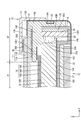
- FIG. Exploded perspective view showing schematic configuration of liquid crystal display device Sectional drawing of the cross section which cut
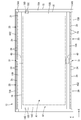
- a plan view of the backlight device viewed from the front side The top view which expanded the site
- Embodiment 2 the top view which expanded the site
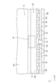
- part which faces between adjacent LED boards among the edge of the light-incidence surface side of the light-projection surface of a light-guide plate, and its vicinity is shown.
- Embodiment 3 the photograph which shows the brightness
- the television receiver 1 includes a liquid crystal display device (an example of a display device) 10, front and back cabinets CA ⁇ b> 1 and CA ⁇ b> 2 that are accommodated so as to sandwich the liquid crystal display device 10, a power source 2, and a tuner 4. And a stand 6.
- a part of each drawing shows an X-axis, a Y-axis, and a Z-axis, and each axis direction is drawn in a common direction in each drawing.
- the X-axis direction coincides with the horizontal direction
- the Y-axis direction coincides with the vertical direction
- the Z-axis direction coincides with the thickness direction (front and back direction).
- the upper side of the figure coincides with the front side of the liquid crystal display device 10.
- the liquid crystal display device 10 has a horizontally long rectangular shape as a whole, and includes a liquid crystal panel (an example of a display panel) 11 and a backlight device (an example of an illumination device) 12 that is an external light source. It is integrally held by the formed bezel 13 or the like.
- the liquid crystal panel 11 is assembled in a posture in which a display surface 11C capable of displaying an image faces the front side.
- the liquid crystal panel 11 in the present embodiment is a high-definition panel having a large number of pixels, a so-called 4K2K panel, and has a large size of, for example, 32 types or more.
- the bezel 13 is made of a metal having excellent rigidity such as stainless steel. As shown in FIGS. 2 and 3, the bezel 13 is parallel to the liquid crystal panel 11 and has a substantially frame shape in plan view.
- the bezel frame-shaped portion 13A includes a bezel tubular portion 13B extending in a substantially short tubular shape from the outer peripheral end portion toward the back side.
- the bezel frame portion 13A extends along the edge of the display surface 11C of the liquid crystal panel 11.
- a buffer material 26A is disposed between the bezel frame-shaped portion 13A and the liquid crystal panel 11 (see FIG. 3), and the bezel frame-shaped portion 13A has the edge of the display surface 11C on the front side through the buffer material 26A.
- the liquid crystal panel 11 is held by pressing from the side.
- the bezel cylindrical portion 13 ⁇ / b> B covers a part of a frame 14 to be described later and constitutes a part of a side appearance of the liquid crystal display device 10.
- the liquid crystal panel 11 has a horizontally long rectangular shape in a plan view, and a predetermined interval is provided between the optical sheet group 16 and the optical sheet group 16 described later. Provided and stacked.
- the liquid crystal panel 11 is configured such that glass substrates 11A and 11B having excellent translucency are bonded together with a predetermined gap therebetween, and liquid crystal is sealed between the substrates 11A and 11B.
- the back side is the array substrate 11A
- the front side is the color filter substrate 11B. As shown in FIG.
- a display area A1 capable of displaying an image is arranged in the majority, and an area outside the display area A1 is a non-display area A2 where no image is displayed.
- a display area A1 capable of displaying an image is arranged on a large part of the display surface 11C, and an area outside the display area A1 forms a frame surrounding the display area A1 and the bezel of the bezel 13
- the non-display area A2 is covered with the frame-like portion 13A and no image is displayed (see FIGS. 3 and 5).
- a polarizing plate (not shown) is disposed outside both the substrates 11A and 11B.
- the array substrate 11A is provided with switching elements (for example, TFTs) connected to mutually orthogonal source lines and gate lines, pixel electrodes connected to the switching elements, and an alignment film.
- the array substrate 11A is provided with a large number of TFTs and pixel electrodes arranged side by side, and a large number of TFTs and pixel electrodes are arranged around the TFTs and pixel electrodes so as to surround a gate wiring and a source wiring in a lattice shape. It is installed.
- the gate wiring and the source wiring are connected to the gate electrode and the source electrode, respectively, and the pixel electrode is connected to the drain electrode of the TFT.
- the color filter substrate 11B is provided with a color filter in which colored portions such as R (red), G (green), and B (blue) are arranged in a predetermined arrangement, a counter electrode, and an alignment film. Yes.
- the array substrate 11A is slightly larger than the color filter substrate 11B so that its outer peripheral end protrudes outward from the outer peripheral end of the color filter substrate 11B over the entire periphery. Is formed.
- a plurality of gate side terminal portions (not shown) routed from the gate wirings described above are provided at both ends on the short side constituting the outer peripheral end of the array substrate 11A.
- a plurality of gate side flexible substrates 28 having flexibility (flexibility) are connected to each gate side terminal portion.
- the one on the long side (the upper right side in FIG. 2) has a source side terminal routed from the above-described source wiring.
- a plurality of parts (not shown) are provided.
- a plurality of source-side flexible substrates 30 having flexibility (flexibility) are connected to these source-side terminal portions.
- the gate side flexible substrate 28 and the source side flexible substrate 30 are made of synthetic resin having insulation and flexibility, respectively.
- a gate driver D1 for driving liquid crystal is mounted on the back surface of the gate side flexible substrate 28, and a source driver D2 is mounted on the back surface of the source side flexible substrate 30.
- Both drivers D1 and D2 have a protruding shape that protrudes inward from the mounting surface, and have a horizontally long shape.
- Both drivers D1 and D2 are composed of LSI chips having a drive circuit therein, and process input signals relating to images supplied from a control board (not shown) as a signal supply source to output output signals. The output signal is output to the liquid crystal panel 11.
- one end of the source side flexible substrate 30 is connected to the array substrate 11A, and the other end is bent and led to the back side of the bottom plate portion 15A of the chassis 15 described later. It is connected to the source substrate 32 arranged on the back side.
- the backlight device 12 is mainly composed of a frame (an example of a frame-like member) 14 that forms the front side appearance of the backlight device 12, and the back side appearance of the backlight device 12. Is accommodated in a space held between the chassis 15 and the chassis 15. Main components housed between the frame 14 and the chassis 15 include at least a light guide plate 18, a reflection sheet 21, and a plurality of LED units 20. The light guide plate 18 is held between the frame 14 and the chassis 15, and the optical sheet group 16 is laminated on the front side of the light guide plate 18. Each LED unit 20 is paired in a space between the frame 14 and the chassis 15 so as to sandwich the light guide plate 18 from both sides in the short side direction.
- the backlight device 12 according to the present embodiment is a so-called edge light type.
- the light guide plate 18 is made of a synthetic resin material (for example, acrylic resin such as PMMA or polycarbonate) having a refractive index sufficiently higher than that of air and substantially transparent (excellent translucency). As shown in FIG. 2, the light guide plate 18 has a horizontally long rectangular shape when viewed in a plane, like the liquid crystal panel 11 and the optical sheet group 16 described later, and the long side direction on the plate surface is the X-axis direction. The short side direction coincides with the Y-axis direction, and the thickness direction perpendicular to the plate surface coincides with the Z-axis direction.
- the light guide plate 18 is supported by a chassis 15 described later. Both end surfaces on the long side of the light guide plate 18 are light incident surfaces 18A on which light emitted from the LED units 20 is incident.
- the light guide plate 18 is in a posture in which the pair of light incident surfaces 18A are opposed to the respective LED units 20, and the light emitting surface 18B, which is the main plate surface (the plate surface on the front side), is directed to the optical sheet group 16 side.
- the opposite surface 18C which is the plate surface opposite to 18B (the plate surface on the back side), is arranged in a posture toward the reflection sheet 21 side described later.
- the light guide plate 18 introduces the light emitted from each LED unit 20 from each light incident surface 18A, rises toward the optical sheet group 16 side while propagating the light inside, and exits from the light exit surface 18B. It has a function to make it.
- a plurality of dot patterns (not shown) for light reflection are provided on the opposite surface 18C of the light guide plate 18.
- notches 18D that are recessed inwardly toward the inner side (center side of the light guide plate 18) are formed in the vicinity of the edge on the light incident surface 18A side on both end surfaces on the short side of the light guide plate 18. Is provided.
- Each notch 18D is provided so as to penetrate the light guide plate 18 in the thickness direction (Z-axis direction) so as to have a rectangular shape in plan view.
- the reflection sheet 21 is a rectangular sheet-like member, made of synthetic resin, and has a white surface with excellent light reflectivity.
- the reflection sheet 21 has a long side direction that coincides with the X-axis direction and a short side direction that coincides with the Y-axis direction, and is in contact with both in a state of being sandwiched between the light guide plate 18 and the chassis 15. is doing.
- the reflection sheet 21 can reflect light leaked from each LED unit 20 or the light guide plate 18 to the surface side of the reflection sheet 21.
- the optical sheet group 16 has a horizontally long rectangular shape when viewed in a plane, similar to the light guide plate 18 and the liquid crystal panel 11, and the size viewed in the plane is a light emitting surface of the light guide plate 18. It is supposed to be slightly smaller than 18B. As shown in FIG. 3, the optical sheet group is arranged so as to overlap the entire display area A ⁇ b> 1 of the liquid crystal panel 11, and its edge portion overlaps the non-display area A ⁇ b> 2 of the liquid crystal panel 11. The optical sheet group 16 is stacked on the light emitting surface 18 ⁇ / b> B of the light guide plate 18 and is disposed at a predetermined interval from the liquid crystal panel 11.
- the optical sheet group 16 is formed by laminating three optical sheets, a diffusion sheet 16A, a prism sheet 16B, and a reflective polarizing sheet 16C, in order from the light guide plate 18 side.
- the optical sheet group 16 is disposed so as to be interposed between the light guide plate 18 and the liquid crystal panel 11, thereby transmitting light emitted from the light guide plate 18 and giving a predetermined optical action to the transmitted light. The light is emitted to the liquid crystal panel 11.
- the chassis 15 constitutes the external appearance of the back side of the liquid crystal display device 10.
- the chassis 15 is made of a metal such as aluminum, and as shown in FIG. 2, the chassis 15 has a generally horizontally shallow shallow plate shape as a whole so as to cover the entire back side of the liquid crystal display device 10.
- the chassis 15 includes a bottom plate portion 15A that covers the back side of the liquid crystal panel 11, and side plate portions 15B that rise from the edges on both long sides of the bottom plate portion 15A to the front side. Further, both end portions on the long side of the bottom plate portion 15A are stepped portions 15A1 that protrude from the bottom plate portion 15A toward the back side of the liquid crystal display device 10 (see FIG. 3). As shown in FIG.
- the side plate portion 15B has a rising dimension (Z-axis direction dimension) substantially equal to the thickness dimension of the light guide plate 18 plus the projecting dimension of the stepped portion 15A1.
- the entire area of the back side of the LED unit 20 (the side opposite to the light emitting side of the LED 24) is covered.
- each positioning portion 15C has the same position in the short side direction (Y-axis direction) of the bottom plate portion 15A, and is perpendicular to the bottom plate portion 15A (Z-axis direction) so as to be the target with the light guide plate 18 in between.
- Each of the positioning portions 15C when viewed in a plan view shown in FIG. 5, fits in each of the cutouts 18D with almost no gap between each portion and the cutouts 18D provided on the light guide plate 18. ing. Thereby, the light guide plate 18 is positioned with respect to the bottom plate portion 15A.
- a sheet-like first heat radiation sheet HS1 having heat radiation properties is disposed between the bottom plate part 15A of the chassis 15 and the source substrate 32, as shown in FIG. 4, a sheet-like first heat radiation sheet HS1 having heat radiation properties is disposed between the bottom plate part 15A of the chassis 15 and the source substrate 32, as shown in FIG. 4, a sheet-like first heat radiation sheet HS1 having heat radiation properties is disposed between the bottom plate part 15A of the chassis 15 and the source substrate 32, as shown in FIG. 4, a sheet-like first heat radiation sheet HS1 having heat radiation properties is disposed between the bottom plate part 15A of the chassis 15 and the source substrate 32, as shown in FIG. 4, a sheet-like first heat radiation sheet HS1 having heat radiation properties is disposed between the bottom plate part 15A of the chassis 15 and the source substrate 32, as shown in FIG. 4, a sheet-like first heat radiation sheet HS1 having heat radiation properties is disposed between the bottom plate part 15A of the chassis 15 and the source substrate 32, as shown in FIG. 4, a
- the frame 14 is formed in a horizontally long frame shape like the bezel 13 and is made of synthetic resin.
- the frame 14 is parallel to the liquid crystal panel 11 and has a substantially frame shape in a plan view, and a frame extending in a substantially short tube shape from the outer peripheral end of the frame frame portion 14A toward the front and back sides. It consists of the cylindrical part 14B.
- 14 A of frame frame-shaped parts are extended along the edge of the light-projection surface 18B of the light-guide plate 18, The one part presses the outermost edge part among the edges of the light-projection surface 18B from a front side, and is a chassis.
- the light guide plate 18 is sandwiched between the 15 bottom plate portions 15A.
- the frame frame-like portion 14A is provided with a cover portion 14A1 that covers the edge of the light emitting surface 18B and the edge of the optical sheet group 16 from the front side by protruding inward from the portion sandwiching the light guide plate 18. (See FIG. 4).
- a buffer material 26B is disposed between the frame frame-shaped portion 14A and the liquid crystal panel 11, and the frame frame-shaped portion 14A supports the edge of the liquid crystal panel 11 from the back side via the buffer material 26B. ing.
- the length of the part extending from the outer peripheral end of the frame frame part 14A to the back side of the frame cylindrical part 14B is longer than the length of the part extending to the front side.
- the portion extending to the back side is assigned to most of both side plate portions 15B of the chassis 15 and constitutes a part of the appearance of the side surface of the liquid crystal display device 10.
- a portion of the frame cylindrical portion 14B that is addressed to one side plate portion 15B is provided with a concave driver accommodating portion 14B1 that opens to the outside and accommodates the source driver D1 (see FIG. 4). ).
- the source driver D2 is accommodated in the driver accommodating portion 14B1 while maintaining a non-contact state with respect to the driver accommodating portion 14B1. Thereby, most of the heat generated in the source driver D2 due to the driving of the source driver D2 is propagated to the mounting portion of the source driver D2 on the source-side flexible substrate 30.
- each LED unit 20 includes an LED substrate 25 and a plurality of LEDs 24 mounted on the LED substrate 25.
- the LED 24 constituting each LED unit 20 is configured such that an LED chip (not shown) is sealed with a resin material on a substrate portion fixed to the LED substrate 25.
- the LED chip mounted on the substrate unit has one main emission wavelength, and specifically, one that emits blue light in a single color is used.
- the resin material for sealing the LED chip is dispersed and blended with a phosphor that emits a predetermined color when excited by blue light emitted from the LED chip, and generally emits white light as a whole. Is done.
- a yellow phosphor that emits yellow light for example, a green phosphor that emits green light, and a red phosphor that emits red light are used in appropriate combination, or any one of them is used. It can be used alone.
- the LED 24 is a so-called top surface light emitting type in which a surface opposite to a surface on which the LED substrate 25 is mounted is a main light emitting surface.
- the LED substrate 25 that constitutes the LED unit 20 is made of aluminum having excellent heat dissipation, and as shown in FIGS. 2 and 5, is elongated and extends along the long side direction (X-axis direction) of the light guide plate 18. It has a plate shape and is vertically supported by the step portion 15A1 of the bottom plate portion 15A of the chassis 15. Specifically, the LED substrate 25 is arranged with its plate surface parallel to the X-axis direction and Z-axis direction, that is, the posture parallel to the light incident surface 18A of the light guide plate 18.
- Each LED substrate 25 has a length in the long side direction (X-axis direction) that is about half the size in the long side direction of the light guide plate 20, and has a predetermined length along the light incident surface 18 ⁇ / b> A of the light guide plate 18. Two are arranged side by side at intervals. Each LED board 25 has a short side direction dimension substantially equal to the thickness dimension of the light guide plate 18 plus the projecting dimension of the step portion 15A1 (see FIG. 3).
- a plurality of LEDs 24 are surface-mounted on a plate surface inside the LED substrate 25, that is, a plate surface facing the light guide plate 18, and this surface is a mounting surface 25A.
- Each LED 24 is disposed by being soldered directly to the mounting surface 25A of the LED substrate 25 with its light emitting surface 24A facing the light incident surface 18A of the light guide plate 18.
- the LEDs 24 are arranged in a line (linearly) at a substantially equal pitch along the length direction (X-axis direction) on the mounting surface 25 ⁇ / b> A of the LED substrate 25.
- a wiring pattern (not shown) that is made of a metal film (such as copper stay) and supplies driving power to each LED 24 is formed.
- seat HS2 which has heat dissipation is distribute
- the second heat radiating sheet HS2 is in contact with both between the LED board 25 and the side plate portion 15B, whereby a part of the heat propagated to the LED board 25 passes through the second heat radiating sheet HS2. It is configured to be effectively propagated to the side plate portion 15B.
- a light reflecting member 40 having light reflectivity is arranged on a part of the back side of the cover portion 14 ⁇ / b> A ⁇ b> 1 in the frame frame-like portion 14 ⁇ / b> A of the frame 14. ing.
- the light reflecting member 40 has a sheet shape, and one surface has adhesiveness so that the light reflecting member 40 is affixed to the covering portion 14A1.
- the light reflecting member 40 is a portion facing the S ⁇ b> 1 between the LED substrates 25 adjacent to each other on the light incident surface 18 ⁇ / b> A side edge of the light emitting surface 18 ⁇ / b> B of the light guide plate 18.
- each light reflecting member 40 is arranged in the form facing each other. As shown in FIG. 5, in the plan view of the backlight device 12, most of each light reflecting member 40 faces the light emitting surface 18 ⁇ / b> B of the light guide plate 18, and a part of the light reflecting member 40 overlaps with the optical sheet group 16. ing. Further, as shown in FIG. 5, each light reflecting member 40 is arranged in the vicinity of the boundary portion with the display area A ⁇ b> 1 in the non-display area A ⁇ b> 2 of the liquid crystal panel 11.
- the interval between the adjacent LEDs 24 at S ⁇ b> 1 between the two adjacent LED substrates 25 is mounted on the mounting surface 25 ⁇ / b> A of the LED substrate 25. It becomes larger than the interval between the LEDs 24.
- the light reflecting member 40 described above is not provided, when the edge of the light emitting surface 18B of the light guide plate 18 on the light incident surface 18A side is viewed, the adjacent LED substrate 25 among the edges.
- the part that faces S1 during the period may be displayed relatively darker than other parts, and a dark part may occur in the part that faces. And when this dark part arises to a part of display area A1 of the liquid crystal panel 11, the brightness nonuniformity resulting from the said dark part arises in the image displayed on the display surface 11C.
- the light that has reached the light reflecting member 40 is exposed to the portion facing the S1 between the adjacent LED substrates 25 on the light incident surface 18A side edge of the light emitting surface 18B of the light guide plate 18 by the light reflecting member 40. Reflected.
- the reflected light reaches the dark part generated in the vicinity and the vicinity thereof, and the dark part generated in the display area A1 in addition to the dark part generated in the non-display area A2 can be eliminated.
- the optical sheet interferes with the light reflecting member when the optical sheet group disposed on the light emitting surface undergoes thermal expansion or the like. There is a risk of doing.
- the light reflecting member 40 is attached to a part of the frame 14, that is, the covering portion 14A1 of the frame 14. For this reason, it can suppress that the light reflection member 40 interferes with another member resulting from the thermal expansion etc. of another member.
- ⁇ Modification 1 of Embodiment 1> A first modification of the first embodiment will be described with reference to FIG.
- the number of LED units 120 provided in the backlight device 112 and the number of light reflecting members 140 are different from those in the first embodiment. Other configurations are the same as those in the first embodiment.
- the backlight device 112 according to this modification as shown in FIG. 7, six LED units 20 are accommodated in the chassis 15. That is, the length dimension of the LED substrate 125 constituting each LED unit 120 is shorter than that of the first embodiment, and each LED substrate 125 has a predetermined interval along the light incident surface 18A of the light guide plate 18. Three are arranged side by side while being vacant. Further, four light reflecting members 140 are accommodated in the chassis 15.
- each light reflecting member 140 is arranged in a form facing the portion facing the S ⁇ b> 2 between the adjacent LED substrates 125 on the light incident surface 18 ⁇ / b> A side edge of the light emitting surface 18 ⁇ / b> B of the light guide plate 18. .
- each light out of the light emitted from the light emitting surface 18B of the light guide plate 18 is used.
- the light reaching the reflecting member 140 is reflected by the light reflecting member 140 to a portion facing the S2 between the adjacent LED substrates 125 in the edge on the light incident surface 18A side of the light emitting surface 18B of the light guide plate 18. .
- the reflected light reaches the dark part generated in the vicinity and the vicinity thereof, and the dark part generated in the display area A1 in addition to the dark part generated in the non-display area A2 can be eliminated. It can suppress that the brightness nonuniformity resulting from the said dark part arises in the image displayed on a surface.
- ⁇ Modification 2 of Embodiment 1> A second modification of the first embodiment will be described.
- the cover portion of the frame in which the light reflecting member 40 is disposed in Embodiment 1 in the frame is painted white so that the entire cover portion has light reflectivity. It is a light reflecting member. For this reason, the sheet-like light reflection member is not arranged in the covering part.
- the cover portion since the cover portion is painted in white as a light reflecting member in this way, the thickness of the light reflecting member becomes equal to the thickness of the coating. The thickness of the light reflecting member can be reduced as compared with the case where the reflecting member is provided. As a result, the backlight device can be thinned.
- the arrangement of the light reflecting members 240 is different from that of the first embodiment. Since other configurations are the same as those of the first embodiment, description thereof is omitted.
- the light reflecting member 240 is attached to the light emitting surface 18 ⁇ / b> B of the light guide plate 18. Specifically, as shown in FIG. 9, the light reflecting member 240 is attached to a portion of the light emitting surface 18 ⁇ / b> B of the light guide plate 18 on the light incident surface 18 ⁇ / b> A side facing the S ⁇ b> 3 between the adjacent LED substrates 25. Are arranged.
- the light reflecting member since the light reflecting member is arranged as described above, light that is about to be emitted from a portion of the light emitting surface 18B of the light guide plate 18 to which each light reflecting member 240 is attached. However, the light reflecting member 240 reflects the portion of the light guide plate 18 facing the S3 between the adjacent LED substrates 125 and the vicinity thereof. Thereby, the reflected light reaches the part facing the S3 between the adjacent LED substrates 25 and the dark part generated in the vicinity of the edge on the light incident surface 18A side of the light emitting surface 18B of the light guide plate 18.
- FIG. 10 Illustrate the photo.
- A3 the brightness difference is hardly seen compared with the other part of the light-projection surface 18B of the light-guide plate 18.
- the light reflecting member 240 is disposed, so that the dark portion generated in the display region A1 in addition to the dark portion generated in the non-display region A2 of the liquid crystal panel 11 is eliminated.
- the plurality of circular patterns visible on the light guide plate 18 are dot patterns for light reflection provided on the opposite surface 18 ⁇ / b> C of the light guide plate 18.
- Embodiment 3 will be described with reference to FIGS.
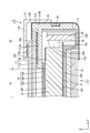
- a protruding portion (an example of a light scattering member) 316D that protrudes in a convex shape toward the LED substrate 25 side is provided on a part of the side edge.
- the protruding portion 316D is provided so as to face a portion facing the S4 between the adjacent LED substrates 25 on the light incident surface 18A side edge of the light emitting surface 18B of the light guide plate 18. Has scattering properties. Further, as shown in FIG. 12, the protrusion 316D is located in the vicinity of the boundary with the display area A1 in the non-display area A2 of the liquid crystal panel 311. In addition, about the other structure of the liquid crystal display device 310 which concerns on this embodiment, since it is the same as that of Embodiment 1, description is abbreviate
- the protruding portion 316D having light scattering properties is provided in the above-described arrangement manner, so that the protruding portion of the light emitted from the light emitting surface 18B of the light guide plate 18 is provided.
- the light that has reached 316D is scattered by the protrusion 316D to a portion facing the S4 between the adjacent LED substrates 25 on the light incident surface 18A side edge of the light exit surface 18B of the light guide plate 18.
- the protrusion 316D is scattered in the facing part and its vicinity, and the brightness of the dark part generated in the facing part and its vicinity is increased, and the difference in brightness between the dark part and the other part is reduced.
- FIG. 13 shows the luminance in the vicinity of the portion facing the S4 between the adjacent LED substrates 25 on the light incident surface 18A side edge of the light emitting surface 18B of the light guide plate 18 in this embodiment. Illustrate the photo.
- A4 compared with the other part of the light-projection surface 18B of the light-guide plate 18, a brightness difference is hardly seen.
- the projection 316D is provided on the prism sheet 316B of the optical sheet group 316, so that the dark part generated in the display area A1 in addition to the dark part generated in the non-display area A2 of the liquid crystal panel 11 is eliminated. .
- the protrusions are provided so as to overlap all the optical sheets constituting the optical sheet group 416 in this way, compared with that of the fourth embodiment.
- the effect of scattering light that reaches the protrusion 416D is enhanced.
- light is further scattered by the protrusions 416D at the portion facing the adjacent LED substrate 25 and the vicinity thereof on the light incident surface 18A side edge of the light emitting surface 18B of the light guide plate 18.
- the brightness of the dark part generated in the region and the vicinity thereof is further increased. As a result, it is possible to effectively suppress the occurrence of luminance unevenness due to the dark portion in the image displayed on the display surface of the liquid crystal panel 11.
- ⁇ Modification 2 of Embodiment 3> A first modification of the third embodiment will be described with reference to FIG.
- the projection 416D is provided only on the prism sheet 416B among the optical sheets constituting the optical sheet group 416 as in the fourth embodiment.
- a light reflecting member 540 having the same configuration as that of the light reflecting member 40 described in the first embodiment is attached to the back side of the protruding portion 416D (the side facing the light emitting surface 18B of the light guide plate 18). Yes.
- the same effect as that of the backlight device 12 of the first embodiment can be obtained by adopting such a configuration. That is, the light that has reached the light reflecting member 540 out of the light emitted from the light emitting surface 18B of the light guide plate 18 is caused to end by the light reflecting member 540 on the light incident surface 18A side of the light emitting surface 18B of the light guide plate 18. It is reflected by the site
- each modification of the first embodiment, and the second embodiment as an example of the light reflecting member, a sheet-like member and a part of the frame that are painted white are exemplified.
- the reflection member is not limited as long as it has light reflectivity.
- the configuration in which the protruding portion protruding in a convex shape is provided in a part of the optical sheet group is illustrated, but the shape of the protruding portion is not limited. .
- the protruding portion may be provided in a shape protruding in a semicircular shape, or may be provided in a shape protruding in a triangular shape.
- the protrusions provided in a part of the optical sheet group are exemplified as an example of the light scattering member.
- the configuration of the light scattering member is not limited.
- the backlight device may separately include a light scattering member such as a sheet.
- each end face on both long sides of each end face of the light guide plate is a light incident face
- the configuration in which the LED substrate is arranged to face each light incident face is exemplified.
- all the end faces of the light guide plate may be light incident surfaces, and the LED substrate may be arranged to face each light incident surface.
- the light reflecting member or the light scattering member in a form facing the portion facing between the adjacent LED substrates among the edges on the light incident surface side of the light emitting surface of the light guide plate, It can suppress that the brightness nonuniformity resulting from the said dark part arises in the image displayed on the display surface of a liquid crystal panel.
- a high-definition liquid crystal panel has been exemplified.
- the present invention can also be applied to a display panel that is not high-definition.
- the present invention it is possible to suppress the occurrence of luminance unevenness due to the dark portion in the image displayed on the display surface of the liquid crystal panel. it can.
- a television receiving device of a type including a cabinet is illustrated, but the present invention is applicable to a type not including a cabinet.
- a television receiver including a high-definition liquid crystal panel has been exemplified.
- the present invention can be applied to display devices other than the television receiver.
Landscapes
- Physics & Mathematics (AREA)
- General Physics & Mathematics (AREA)
- Optics & Photonics (AREA)
- Nonlinear Science (AREA)
- Mathematical Physics (AREA)
- Chemical & Material Sciences (AREA)
- Crystallography & Structural Chemistry (AREA)
- Engineering & Computer Science (AREA)
- Microelectronics & Electronic Packaging (AREA)
- Planar Illumination Modules (AREA)
Abstract
Un dispositif d'éclairage (12) est pourvu : de sources de lumière (24) ; d'une plaque de guidage de lumière (18) formée de telle sorte qu'au moins une surface d'extrémité de celle-ci est conçue sous la forme d'une surface d'entrée de lumière (18A) à travers laquelle pénètre la lumière provenant des sources de lumière (24), et qu'une autre surface de plaque est conçue sous la forme d'une surface de sortie de lumière (18B) à travers laquelle est autorisée à sortir la lumière qui a pénétré à partir de la surface d'entrée de lumière (18A) ; d'une pluralité de substrats de source de lumière (25) conçus de telle sorte qu'une surface de plaque est conçue sous la forme d'une surface de montage (25A) sur laquelle sont montées une pluralité de sources de lumière (24), la pluralité de substrats de source de lumière étant disposés le long de la surface d'entrée de lumière (18A) de telle sorte que les surfaces de montage soient orientées vers la surface d'entrée de lumière (18A) ; et d'un élément de réflexion de lumière (40) ayant des propriétés de réflexion de lumière, l'élément de réflexion de lumière (40) étant disposé de manière à faire face à un emplacement sur le bord externe côté surface d'entrée de lumière (18A) de la surface de sortie de lumière (18B) qui est orientée vers un espace (S1) entre des substrats de source de lumière (25) adjacents.
Priority Applications (2)
| Application Number | Priority Date | Filing Date | Title |
|---|---|---|---|
| CN201680026330.5A CN107532785A (zh) | 2015-05-08 | 2016-04-27 | 照明装置、显示装置、以及电视接收装置 |
| US15/572,097 US20180143496A1 (en) | 2015-05-08 | 2016-04-27 | Lighting device, display device, and television device |
Applications Claiming Priority (2)
| Application Number | Priority Date | Filing Date | Title |
|---|---|---|---|
| JP2015-095498 | 2015-05-08 | ||
| JP2015095498 | 2015-05-08 |
Publications (1)
| Publication Number | Publication Date |
|---|---|
| WO2016181838A1 true WO2016181838A1 (fr) | 2016-11-17 |
Family
ID=57248908
Family Applications (1)
| Application Number | Title | Priority Date | Filing Date |
|---|---|---|---|
| PCT/JP2016/063179 Ceased WO2016181838A1 (fr) | 2015-05-08 | 2016-04-27 | Dispositif d'éclairage, dispositif d'affichage, et récepteur de télévision |
Country Status (3)
| Country | Link |
|---|---|
| US (1) | US20180143496A1 (fr) |
| CN (1) | CN107532785A (fr) |
| WO (1) | WO2016181838A1 (fr) |
Cited By (2)
| Publication number | Priority date | Publication date | Assignee | Title |
|---|---|---|---|---|
| CN107357068A (zh) * | 2017-07-21 | 2017-11-17 | 武汉华星光电技术有限公司 | 一种窄边框显示面板及制造方法 |
| WO2020203941A1 (fr) * | 2019-03-29 | 2020-10-08 | シチズン電子株式会社 | Rétro-éclairage |
Families Citing this family (4)
| Publication number | Priority date | Publication date | Assignee | Title |
|---|---|---|---|---|
| CN107908042A (zh) * | 2017-12-28 | 2018-04-13 | 惠州市华星光电技术有限公司 | 液晶模组以及液晶显示装置 |
| CN109541834B (zh) * | 2018-12-29 | 2021-11-02 | 厦门天马微电子有限公司 | 显示面板及显示装置 |
| US12130466B2 (en) * | 2023-01-20 | 2024-10-29 | Samsung Electronics Co., Ltd. | Display apparatus |
| CN221351904U (zh) * | 2023-11-16 | 2024-07-16 | 深圳市玛威尔显控科技有限公司 | 一种高亮度显示屏 |
Citations (6)
| Publication number | Priority date | Publication date | Assignee | Title |
|---|---|---|---|---|
| JP2004296372A (ja) * | 2003-03-28 | 2004-10-21 | Casio Comput Co Ltd | 表示装置用バックライト |
| JP2012089291A (ja) * | 2010-10-18 | 2012-05-10 | Mitsubishi Electric Corp | 照明用光源及び照明装置 |
| WO2012165248A1 (fr) * | 2011-05-30 | 2012-12-06 | シャープ株式会社 | Appareil d'éclairage, appareil d'affichage et récepteur de télévision |
| JP2014041761A (ja) * | 2012-08-22 | 2014-03-06 | Sharp Corp | 照明装置、表示装置及びテレビ受信装置 |
| EP2743573A1 (fr) * | 2012-12-12 | 2014-06-18 | Boe Technology Group Co. Ltd. | Module de rétroéclairage et dispositif d'affichage |
| JP2014150049A (ja) * | 2013-01-11 | 2014-08-21 | Keio Gijuku | 照明モジュール |
Family Cites Families (10)
| Publication number | Priority date | Publication date | Assignee | Title |
|---|---|---|---|---|
| US20090326510A1 (en) * | 2008-06-30 | 2009-12-31 | Haefner Paul A | Drug Delivery Methods and Systems |
| US20120287355A1 (en) * | 2010-02-02 | 2012-11-15 | Sharp Kabushiki Kaisha | Lighting device, display device, and television receiver |
| US8459857B2 (en) * | 2010-04-26 | 2013-06-11 | Mitsubishi Electric Corporation | Planar light source device and display apparatus using the same |
| KR20130123509A (ko) * | 2012-05-03 | 2013-11-13 | 희성전자 주식회사 | 측면 조광형 백라이트 장치 |
| CN102767762B (zh) * | 2012-07-27 | 2014-10-29 | 深圳市华星光电技术有限公司 | 背光模组 |
| US9494722B2 (en) * | 2012-07-27 | 2016-11-15 | Shenzhen China Star Optoelectronics Technology Co., Ltd | Backlight module |
| EP2713200B1 (fr) * | 2012-09-26 | 2015-10-28 | LG Display Co., Ltd. | Dispositif d'affichage à cristaux liquides |
| TW201500815A (zh) * | 2013-06-17 | 2015-01-01 | Primax Electronics Ltd | 背光模組 |
| CN103823319B (zh) * | 2014-03-10 | 2016-03-09 | 深圳市华星光电技术有限公司 | 背光模组及用该背光模组的液晶显示装置 |
| KR101538366B1 (ko) * | 2014-07-30 | 2015-07-22 | 삼성전자주식회사 | 디스플레이 어셈블리 및 디스플레이 어셈블리를 이용하는 디스플레이 장치 |
-
2016
- 2016-04-27 US US15/572,097 patent/US20180143496A1/en not_active Abandoned
- 2016-04-27 WO PCT/JP2016/063179 patent/WO2016181838A1/fr not_active Ceased
- 2016-04-27 CN CN201680026330.5A patent/CN107532785A/zh active Pending
Patent Citations (6)
| Publication number | Priority date | Publication date | Assignee | Title |
|---|---|---|---|---|
| JP2004296372A (ja) * | 2003-03-28 | 2004-10-21 | Casio Comput Co Ltd | 表示装置用バックライト |
| JP2012089291A (ja) * | 2010-10-18 | 2012-05-10 | Mitsubishi Electric Corp | 照明用光源及び照明装置 |
| WO2012165248A1 (fr) * | 2011-05-30 | 2012-12-06 | シャープ株式会社 | Appareil d'éclairage, appareil d'affichage et récepteur de télévision |
| JP2014041761A (ja) * | 2012-08-22 | 2014-03-06 | Sharp Corp | 照明装置、表示装置及びテレビ受信装置 |
| EP2743573A1 (fr) * | 2012-12-12 | 2014-06-18 | Boe Technology Group Co. Ltd. | Module de rétroéclairage et dispositif d'affichage |
| JP2014150049A (ja) * | 2013-01-11 | 2014-08-21 | Keio Gijuku | 照明モジュール |
Cited By (2)
| Publication number | Priority date | Publication date | Assignee | Title |
|---|---|---|---|---|
| CN107357068A (zh) * | 2017-07-21 | 2017-11-17 | 武汉华星光电技术有限公司 | 一种窄边框显示面板及制造方法 |
| WO2020203941A1 (fr) * | 2019-03-29 | 2020-10-08 | シチズン電子株式会社 | Rétro-éclairage |
Also Published As
| Publication number | Publication date |
|---|---|
| CN107532785A (zh) | 2018-01-02 |
| US20180143496A1 (en) | 2018-05-24 |
Similar Documents
| Publication | Publication Date | Title |
|---|---|---|
| KR101337072B1 (ko) | 백라이트 유닛 및 이를 구비한 액정표시장치 | |
| KR101754288B1 (ko) | 표시모듈을 포함하는 보더리스 표시장치 | |
| US9632237B2 (en) | Illumination device, display device, and TV receiver | |
| CN110058452B (zh) | 照明装置和显示装置 | |
| WO2013035601A1 (fr) | Dispositif d'éclairage, dispositif d'affichage et dispositif de réception de télévision | |
| US9417379B2 (en) | Image display device and television reception device | |
| WO2015141368A1 (fr) | Dispositif d'affichage et dispositif récepteur de télévision | |
| JP7123701B2 (ja) | 電子機器 | |
| WO2016181838A1 (fr) | Dispositif d'éclairage, dispositif d'affichage, et récepteur de télévision | |
| WO2014021304A1 (fr) | Dispositif d'éclairage, dispositif d'affichage, et dispositif de réception de télévision | |
| WO2014073425A1 (fr) | Dispositif d'éclairage, dispositif d'affichage, et dispositif récepteur de télévision | |
| WO2015002083A1 (fr) | Dispositif d'éclairage, dispositif d'affichage et dispositif de réception de télévision | |
| WO2013039001A1 (fr) | Dispositif d'éclairage, dispositif d'affichage et dispositif de réception de télévision | |
| WO2013129244A1 (fr) | Dispositif d'affichage et récepteur de télévision | |
| WO2014017346A1 (fr) | Dispositif d'affichage et récepteur de télévision | |
| WO2011067994A1 (fr) | Dispositif d'éclairage, dispositif d'affichage, et dispositif de réception de télévision | |
| JP2013218055A (ja) | 表示装置、及びテレビ受信装置 | |
| US20150103258A1 (en) | Lighting device, display device and television device | |
| WO2011092953A1 (fr) | Dispositif d'éclairage, écran et dispositif de téléviseur | |
| WO2013047367A1 (fr) | Dispositif d'affichage et dispositif de réception de télévision | |
| JP5715966B2 (ja) | 表示装置及びテレビ受信装置 | |
| WO2014141882A1 (fr) | Appareil d'affichage et appareil récepteur de télévision | |
| WO2014199669A1 (fr) | Dispositif d'éclairage, dispositif d'affichage et dispositif de réception tv | |
| JP2013171619A (ja) | 表示装置及びテレビ受信装置 | |
| JP2013206574A (ja) | 照明装置、表示装置、及びテレビ受信装置 |
Legal Events
| Date | Code | Title | Description |
|---|---|---|---|
| 121 | Ep: the epo has been informed by wipo that ep was designated in this application |
Ref document number: 16792563 Country of ref document: EP Kind code of ref document: A1 |
|
| WWE | Wipo information: entry into national phase |
Ref document number: 15572097 Country of ref document: US |
|
| NENP | Non-entry into the national phase |
Ref country code: DE |
|
| 122 | Ep: pct application non-entry in european phase |
Ref document number: 16792563 Country of ref document: EP Kind code of ref document: A1 |
|
| NENP | Non-entry into the national phase |
Ref country code: JP |