WO2016189860A1 - Connecteur et dispositif de conversion photoélectrique le comprenant - Google Patents
Connecteur et dispositif de conversion photoélectrique le comprenant Download PDFInfo
- Publication number
- WO2016189860A1 WO2016189860A1 PCT/JP2016/002508 JP2016002508W WO2016189860A1 WO 2016189860 A1 WO2016189860 A1 WO 2016189860A1 JP 2016002508 W JP2016002508 W JP 2016002508W WO 2016189860 A1 WO2016189860 A1 WO 2016189860A1
- Authority
- WO
- WIPO (PCT)
- Prior art keywords
- optical fiber
- photoelectric conversion
- connector
- core wire
- fixing
- Prior art date
- Legal status (The legal status is an assumption and is not a legal conclusion. Google has not performed a legal analysis and makes no representation as to the accuracy of the status listed.)
- Ceased
Links
Images










Classifications
-
- G—PHYSICS
- G02—OPTICS
- G02B—OPTICAL ELEMENTS, SYSTEMS OR APPARATUS
- G02B6/00—Light guides; Structural details of arrangements comprising light guides and other optical elements, e.g. couplings
- G02B6/24—Coupling light guides
- G02B6/42—Coupling light guides with opto-electronic elements
- G02B6/43—Arrangements comprising a plurality of opto-electronic elements and associated optical interconnections
-
- H—ELECTRICITY
- H10—SEMICONDUCTOR DEVICES; ELECTRIC SOLID-STATE DEVICES NOT OTHERWISE PROVIDED FOR
- H10F—INORGANIC SEMICONDUCTOR DEVICES SENSITIVE TO INFRARED RADIATION, LIGHT, ELECTROMAGNETIC RADIATION OF SHORTER WAVELENGTH OR CORPUSCULAR RADIATION
- H10F77/00—Constructional details of devices covered by this subclass
- H10F77/40—Optical elements or arrangements
Definitions
- the present disclosure relates to a connector and a photoelectric conversion device having the connector, and more particularly to a connector for converting an electric signal and an optical signal and a photoelectric conversion device having the connector.
- photoelectric conversion devices that convert electrical signals and optical signals have been developed. Since such a photoelectric conversion device transmits data using an optical fiber, data can be transmitted at a higher speed than when data is transmitted using an electric wire. Such a photoelectric conversion device is also excellent in electrical insulation.
- the optical fiber when an external force is applied or when the temperature changes, the optical fiber may expand and contract, thereby applying tension to the optical fiber. In such a case, since the tip of the optical fiber core wire is fixed to the photoelectric conversion unit, the optical fiber core wire may be disconnected.
- an optical transmission module having a configuration in which the optical fiber core wire is bent is known (for example, see Patent Document 1).
- a connector that performs photoelectric conversion by being connected to an optical fiber includes a photoelectric conversion unit, a fixed device, and a housing.
- the photoelectric conversion unit converts electrical signals and optical signals.
- the fixing device has a first surface, a second surface different from the first surface, and a through hole.
- the first surface is a surface facing the photoelectric conversion unit.
- the through hole penetrates the first surface and the second surface.
- the housing houses the photoelectric conversion unit and the fixed device so that the photoelectric conversion unit and the fixed device are arranged in the first direction.
- the through hole is in contact with the first surface at the first opening.
- the length of the opening in the second direction orthogonal to the first direction in the first opening is longer than the length of the opening in the direction orthogonal to the first direction other than the second direction.
- the photoelectric conversion device of the present disclosure includes the above connector and an optical fiber.
- the optical fiber has an optical fiber core and a coating that covers the optical fiber core.
- the optical fiber transmits an optical signal from the connector.
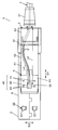
- FIG. 1 is an external view of a photoelectric conversion apparatus according to the first embodiment.
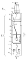
- FIG. 2 is an external view of a main part of the photoelectric conversion apparatus according to the first embodiment.
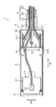
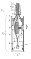
- FIG. 3 is a cross-sectional view of a main part of the photoelectric conversion apparatus according to the first embodiment.
- FIG. 4A is a front view of the photoelectric conversion module. 4B is a cross-sectional view taken along line 4B-4B of FIG. 4A.
- FIG. 5A is a front view of another photoelectric conversion module. 5B is a cross-sectional view taken along line 5B-5B of FIG. 5A.
- FIG. 6 is an exploded perspective view of the fixing device according to the first embodiment.
- FIG. 7A is an external view of a fixing member according to the first embodiment.
- FIG. 7B is an external view of the fixing member according to the first embodiment.
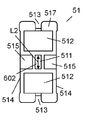
- FIG. 8A is a front view of the fixing member according to the first embodiment.
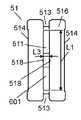
- FIG. 8B is a left side view of the fixing member according to the first embodiment.
- FIG. 8C is a right side view of the fixing member according to the first embodiment.
- FIG. 8D is a top view of the fixing member according to the first embodiment.
- 8E is a cross-sectional view taken along line 8E-8E in FIG. 8D.
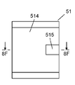
- 8F is a cross-sectional view taken along line 8F-8F in FIG. 8A.
- FIG. 9A is an external view of a pressing member according to the first embodiment.
- FIG. 9B is an external view of the pressing member according to the first embodiment.
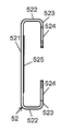
- FIG. 10A is a front view of the pressing member according to the first embodiment.
- FIG. 10B is a left side view of the pressing member according to the first embodiment.
- 10C is a cross-sectional view taken along line 10C-10C of FIG. 10A.
- FIG. 11 is a diagram illustrating a state in the middle of fixing the optical fiber according to the first embodiment to the fixing device.
- FIG. 12 is a diagram illustrating a state in which the optical fiber according to the first embodiment is fixed to a fixing device.
- 13 is a cross-sectional view taken along line 13-13 in FIG.
- FIG. 14 is a cross-sectional view of a main part of the photoelectric conversion device according to the second embodiment.
- FIG. 15 is a cross-sectional view of a main part of the photoelectric conversion device according to the third embodiment.
- FIG. 16 is a cross-sectional view of a main part of a photoelectric conversion device according to a modification of the third embodiment.
- FIG. 17 is an external view of a main part of the photoelectric conversion apparatus according to the fourth embodiment.
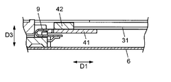
- FIG. 18 is a cross-sectional view of a main part of the photoelectric conversion device according to the fourth embodiment.
- FIG. 19 is a cross-sectional view of a main part of the photoelectric conversion device according to the fourth embodiment.
- FIG. 1 is an external view of a photoelectric conversion apparatus 1 according to the first embodiment.
- FIG. 2 is an external view of a main part of the photoelectric conversion device 1 according to the first embodiment.
- FIG. 3 is a cross-sectional view of a main part of the photoelectric conversion apparatus 1 according to the first embodiment.
- the connector 2 is covered with an outer case 23.
- the connector 2 is sometimes referred to as an optical transmission module or a plug.
- the photoelectric conversion device 1 includes a connector 2 and an optical fiber 3.
- the photoelectric conversion device 1 may include two connectors 2 as shown in FIG. In the photoelectric conversion device 1 shown in FIG. 1, two connectors 2 are connected by an optical fiber 3.
- the connector 2 is configured to perform photoelectric conversion.
- the optical fiber 3 is configured to transmit an optical signal from the connector 2.
- the photoelectric conversion device 1 is used in or between devices such as servers, video equipment, industrial equipment, measuring equipment, commercial printing equipment, medical equipment, and the like. More specifically, the photoelectric conversion device 1 is used for signal transmission between substrates in the device, signal transmission between modules in the device, signal transmission between devices, and the like.
- the optical fiber 3 includes an optical fiber core wire 31, a coating 32, and a strength member 33.
- the optical fiber core 31 includes a core having a high refractive index provided in the center portion and a clad having a refractive index lower than that of the core provided around the core.
- the coating 32 is a resin such as vinyl chloride, and covers the optical fiber core wire 31.
- the tensile body 33 is made of, for example, an aramid fiber or a steel wire.
- the strength member 33 is provided between the optical fiber core wire 31 and the coating 32 in order to increase the strength against tension on the optical fiber 3.
- the optical fiber is a general term for an optical fiber cord and an optical fiber cable.
- the connector 2 includes a photoelectric conversion unit 4, a fixing device 5, and a housing 6 (FIGS. 2 and 3).
- the connector 2 may further include a bushing 21, a connector terminal portion 22 (FIG. 2), and an outer case 23 (FIG. 1).
- the photoelectric conversion unit 4 converts an electrical signal into an optical signal, or converts an optical signal into an electrical signal.
- An optical fiber core wire 31 is connected to the photoelectric conversion unit 4. In addition, the optical fiber core wire 31 should just be optically connected to the photoelectric conversion part 4. FIG.
- the photoelectric conversion unit 4 includes a substrate 41 and a photoelectric conversion circuit 45.
- the substrate 41 is a plate-like and hard substrate.
- the photoelectric conversion circuit 45 is mounted on the substrate 41.
- the photoelectric conversion circuit 45 has a photoelectric conversion module 42.
- the photoelectric conversion circuit 45 may further include an IC 43 and a chip component 44.
- the housing 6 is made of metal, for example, and is formed in a box shape having a space 61.
- the housing 6 houses the photoelectric conversion unit 4 and the fixed device 5.
- the housing 6 has a connector terminal portion 22. More specifically, the photoelectric conversion unit 4 is housed on the first end side inside the housing 6 in the first direction D1 in FIG.
- the fixing device 5 is housed on the second end side opposite to the first end inside the housing 6. That is, the housing 6 has the connector terminal part 22, the photoelectric conversion part 4 and the fixing device 5 arranged so that the connector terminal part 22, the photoelectric conversion part 4 and the fixing device 5 are arranged in this order in the first direction D1. Have.
- the length of the housing 6 in the second direction D2 is longer than the length in the third direction D3 (FIG. 13) orthogonal to both the first direction D1 and the second direction D2.
- An opening 62 is formed in the space 61.
- the connector terminal unit 22 includes a plurality of connector terminals 221.
- the connector terminal portion 22 is formed in the housing 6 on the first end side in the first direction D1.
- the plurality of connector terminals 221 are provided side by side in a second direction D2 orthogonal to the first direction D1.
- the bushing 21 is attached in the vicinity of the housing 6 so that the optical fiber 3 is not bent beyond an allowable angle.
- the bushing 21 is made of, for example, resin.
- the outer case 23 includes a body 231 and a cover 232 (FIG. 1).
- the outer case 23 is configured to cover a portion of the housing 6 other than the portion where the connector terminal portion 22 is formed (FIG. 1). That is, the outer case 23 covers a portion of the housing 6 that houses the photoelectric conversion unit 4 and the fixed device 5.
- FIG. 4A is a front view of the photoelectric conversion module 42.
- 4B is a cross-sectional view taken along line 4B-4B of FIG. 4A.
- the photoelectric conversion module 42 includes two photoelectric conversion elements 421 and two connection mechanisms 426 on the silicon substrate 422.
- the connection mechanism 426 includes a mirror 423, a V-shaped groove 424, and a wiring portion 425.
- the mirror 423 is used to bend the optical path.
- the optical fiber core wire 31 is mounted in the groove 424.
- a photoelectric conversion element 421 is connected to the wiring portion 425.
- the wiring part 425 is connected to the photoelectric conversion circuit 45 mounted on the substrate 41.
- the two photoelectric conversion elements 421 and the two connection mechanisms 426 respectively correspond to the two optical fiber cores 31.
- Each of the two connection mechanisms 426 is configured such that the tip of the corresponding optical fiber core wire 31 is connected.
- the photoelectric conversion element 421 is a light emitting element or a light receiving element.
- an optical signal is transmitted bidirectionally between two connectors 2 using two optical fiber cores 31. Therefore, one of the two photoelectric conversion elements 421 is a light emitting element, and the other is a light receiving element.
- the light emitting element for example, a semiconductor laser or a light emitting diode is used.
- the semiconductor laser VCSEL (Vertical Cavity Surface Emitting LASER: vertical cavity surface emitting laser) or the like is used.
- a photodiode is used as the light receiving element.
- the photoelectric conversion element 421 When the photoelectric conversion element 421 is a light emitting element, an optical signal from the photoelectric conversion element 421 is transmitted to the mirror 423. The optical signal is transmitted to the optical fiber core 31 with the optical path bent by 90 ° by the mirror 423. When the photoelectric conversion element 421 is a light receiving element, an optical signal from the optical fiber core wire 31 is transmitted to the mirror 423. The optical signal is transmitted to the photoelectric conversion element 421 after the optical path is bent by 90 ° by the mirror 423.
- the optical signal can be accurately transmitted between the photoelectric conversion element 421 and the optical fiber core wire 31.
- a thin photoelectric conversion module 42 can be configured.
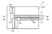
- FIG. 5A is a front view of another photoelectric conversion module 47.
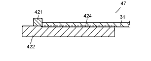
- 5B is a cross-sectional view taken along line 5B-5B of FIG. 5A.
- the photoelectric conversion element 421 may be provided on the silicon substrate 422 so as to emit or receive light in the direction of the groove 424. In this case, an optical signal can be directly transmitted between the photoelectric conversion element 421 and the optical fiber core wire 31.
- the photoelectric conversion circuit 45 mounted on the substrate 41 may include a drive circuit that drives the light emitting element and an amplification circuit that amplifies a signal from the light receiving element.
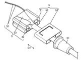
- FIG. 6 is an exploded perspective view of the fixing device 5 according to the first embodiment.
- the fixing device 5 is configured to fix the optical fiber 3 to the housing 6.
- the fixing device 5 includes a fixing member 51 and two pressing members 52.
- FIG. 7A and 7B are external views of the fixing member 51 according to the first embodiment.
- FIG. 8A is a front view of the fixing member 51 according to the first embodiment.
- FIG. 8B is a left side view of the fixing member 51 according to the first embodiment.
- FIG. 8C is a right side view of the fixing member 51 according to the first embodiment.
- FIG. 8D is a top view of the fixing member 51 according to the first embodiment.
- 8E is a cross-sectional view taken along line 8E-8E in FIG. 8D.
- 8F is a cross-sectional view taken along line 8F-8F in FIG. 8A.
- the fixing member 51 has a through hole 511, two recesses 512, two grooves 513, two recesses 514, and two recesses 515.
- the fixing member 51 is made of, for example, resin.
- the fixing member 51 has a first surface 516 on the photoelectric conversion unit 4 side and a second surface 517 different from the first surface 516.
- the second surface 517 is, for example, a surface opposite to the first surface 516.
- the through hole 511 passes through the first surface 516 and the second surface 517.
- the through hole 511 is in contact with the first surface 516 at the opening 601 (first opening).
- the through hole 511 is in contact with the second surface 517 at the opening 602 (second opening).
- the optical fiber core wire 31 (FIGS. 3 and 6) is inserted into the through hole 511.
- a pair of grooves 518 are formed along the first direction D1 on the inner wall of the fixing member 51 in which the through hole 511 is formed.
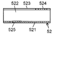
- FIG. 10A is a front view of the pressing member 52 according to the first embodiment.
- FIG. 10B is a left side view of the pressing member 52 according to the first embodiment.
- 10C is a cross-sectional view taken along line 10C-10C of FIG. 10A.
- the fixing device 5 has a pair of pressing members 52.
- the pressing member 52 is formed, for example, by bending a plate-like metal.
- the pressing member 52 includes a base 521, two side parts 522, and two tip parts 523.
- the base 521, the two side portions 522, and the two tip portions 523 are integrally formed.
- a first pressing portion 524 for pressing the coating 32 is formed at the distal end portion 523.
- the first pressing portion 524 has a plurality of protrusions, and the plurality of protrusions presses the covering 32 so that the covering 32 is pressed down.
- the base 521 is formed with a second pressing portion 525 for pressing the strength member 33. Specifically, the tension member 33 is pressed by pressing the fixing member 51 with the second pressing portion 525.
- the pressing member 52 is fixed by being fitted into the fixing member 51.
- the fixing member 51 and the two pressing members 52 are configured to fix the optical fiber 3 to the housing 6 with the coating 32 interposed therebetween. Further, the fixing member 51 and the pressing member 52 are configured to fix the optical fiber 3 to the housing 6 with the strength member 33 interposed therebetween.
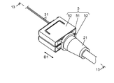
- FIG. 11 is a diagram illustrating a state in the middle of fixing the optical fiber 3 according to the first embodiment to the fixing device 5.
- FIG. 12 is a diagram illustrating a state in which the optical fiber 3 according to the first embodiment is fixed to the fixing device 5.
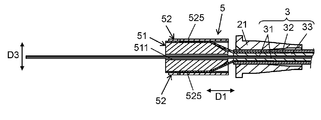
- 13 is a cross-sectional view taken along line 13-13 in FIG.
- the coating 32 and the tension member 33 at the tip of the optical fiber 3 are peeled off so that the tip of the optical fiber 3 is made only of the optical fiber core 31.
- the coating 32 and part of the strength member 33 are separated from the optical fiber core wire 31.
- the optical fiber core wire 31 at the tip of the optical fiber 3 is passed through the through hole 511 of the fixing member 51.
- a part of the coating 32 separated from the optical fiber core wire 31 is inserted into the recess 512 of the fixing member 51.
- a part of the strength member 33 separated from the optical fiber core wire 31 is placed in the concave portion 514 of the fixing member 51.
- the front end 523 of the pressing member 52 is fitted into the groove 513 of the fixing member 51 so that the base 521 of the pressing member 52 covers the concave portion 514 of the fixing member 51.
- the surrounding surfaces of the first pressing portion 524 and the concave portion 512 of the fixing member 51 sandwich the covering 32 inserted into the concave portion 512.
- the covering 32 is fixed to the fixing device 5.
- the second pressing portion 525 and the fixing member 51 of the pressing member 52 sandwich the strength member 33 placed in the recess 514. Thereby, the strength member 33 is fixed to the fixing device 5.
- the optical fiber 3 is fixed to the fixing device 5.
- the optical fiber core 31 at the tip of the optical fiber 3 passes through the through hole 511 of the fixing member 51, and the fixing device 5 is accommodated in the housing 6.
- the optical fiber core 31 at the tip of the optical fiber 3 is installed in the housing 6.
- the optical fiber core wire 31 is connected to the photoelectric conversion unit 4 in the housing 6.
- the fixing device 5 is housed in the housing 6 and fixed. By fixing the optical fiber 3 with a component different from the housing 6, the optical fiber 3 can be easily fixed at the time of assembly. As a result, the optical fiber 3 can be easily aligned.
- the fixing member 51 and the two pressing members 52 fix the covering 32 and the strength member 33 at different positions.
- the covering 32 is fixed by the first pressing portion 524
- the strength member 33 is fixed by the second pressing portion 525.
- the cost can be reduced compared to a structure in which the covering 32 and the strength body 33 are fixed with different parts.
- the tensile strength member 33 becomes slippery due to the elasticity of the coating 32, and the optical fiber 3 may not be sufficiently fixed.
- the place where the covering 32 is fixed and the place where the tensile strength member 33 is fixed are changed, and thus the above-described problem does not occur. That is, the covering 32 and the strength member 33 can be sufficiently fixed. Further, it is preferable to bond the strength member 33 and the covering 32 to the fixing member 51 and the pressing member 52.
- the through-hole 511 of the fixing member 51 is different only in the length of the opening in one direction. It is formed to be longer than the length of the opening in the direction.
- the details of the through hole 511 will be described.
- the through hole 511 of the fixing member 51 has an opening length L1 in the first surface 516 in the second direction D2 orthogonal to the first direction D1. It is formed to be longer than the length of the opening in the first surface 516 in the direction orthogonal to the first direction D1 other than the second direction D2.
- the length L1 is formed to be longer than the length L3 in the third direction D3 (FIG. 6) orthogonal to both the first direction D1 and the second direction D2.
- the through hole 511 of the fixing member 51 has an opening length L1 at the first surface 516 longer than an opening length L2 at the second surface 517 in the second direction D2. Is formed.
- the optical fiber core wire 31 of the optical fiber 3 passes through the through hole 511 as shown in FIGS. 2, 3, and 13.
- the optical fiber core wire 31 can be freely moved within the through hole 511. Thereby, the optical fiber core wire 31 can be bent in the second direction D ⁇ b> 2 within the housing 6.
- the length L4 of the optical fiber core 31 in the housing 6 is longer than the distance L5 between the tip (connection point 35) of the optical fiber core 31 and the end of the housing 6 (FIG. 2).
- the optical fiber core wire 31 When no tension is applied to the optical fiber 3, the optical fiber core wire 31 is bent in the housing 6 by the through hole 511 of the fixing member 51. That is, the optical fiber core wire 31 is bent in the width direction of the housing 6 (second direction D2).
- the optical fiber core wire 31 when a tension is applied to the optical fiber 3, even if the coating 32 extends due to the tension applied to the optical fiber 3, the optical fiber core wire 31 is bent, so that it does not extend straight. Thereby, the possibility of disconnection of the optical fiber core wire 31 is reduced. Further, when the tension on the optical fiber 3 is lost, the optical fiber core wire 31 returns to the state before the tension is applied to the optical fiber 3. That is, the optical fiber core wire 31 bends before tension is applied to the optical fiber 3.
- the direction in which the optical fiber 3 is bent is a direction in which the thin shape of the photoelectric conversion module 42 can be effectively used.
- the second surface 517 is a surface opposite to the first surface 516.
- the second surface 517 is not necessarily opposed to the first surface 516. In other words, the second surface 517 may not be a surface opposite to the first surface 516.
- the optical fiber core 31 passes through the fixing device 5 for fixing the optical fiber 3
- the optical fiber core 31 is moved in a specific direction ( It can be bent in the second direction D2).
- FIG. 14 is a cross-sectional view of a main part of the photoelectric conversion apparatus 110 according to the second embodiment.
- the photoelectric conversion device 110 is different from the photoelectric conversion device 1 (FIG. 3) according to the first embodiment in that it includes the core wire fixing mechanism 7.
- symbol is attached
- the connector 210 of the present embodiment includes a core wire fixing mechanism 7 as shown in FIG.
- the core wire fixing mechanism 7 is configured to fix the optical fiber core wire 31 to the fixing device 5.
- the core wire fixing mechanism 7 includes a core wire fixing member 71, an elastic body 72, and a storage portion 73.
- the core wire fixing member 71 is configured to fix the optical fiber core wire 31.
- the elastic body 72 is a spring, for example, and is a core wire fixing member from the second surface 517 side of the fixing device 5 (fixing member 51) toward the first surface 516 while being stored in the storage portion 73. 71 is pushed into the housing 6.
- the optical fiber core wire 31 By pushing the core wire fixing member 71 by the elastic body 72, the optical fiber core wire 31 can be sufficiently bent in the housing 6. Thereby, after tension is applied to the optical fiber 3, the bending of the optical fiber core 31 can be maintained by pushing the core wire fixing member 71 again so that the optical fiber core 31 is bent.
- the photoelectric conversion device 110 and the connector 210 are configured to push the optical fiber core 31 into the housing 6 by pushing the core fixing member 71 to which the optical fiber 31 is fixed with the elastic body 72. Can be bent.
- FIG. 15 is a cross-sectional view of a main part of the photoelectric conversion device 120 according to the third embodiment.
- the photoelectric conversion device 120 is different from the photoelectric conversion device 1 (FIG. 3) according to the first embodiment in that the photoelectric conversion device 120 includes the elastic mechanism 8.
- symbol is attached
- the connector 220 of this embodiment includes an elastic mechanism 8 in the housing 6 as shown in FIG.
- the elastic mechanism 8 is provided so as to bypass the optical fiber core wire 31 in the housing 6.
- the elastic mechanism 8 of this embodiment is an elastic body 81.
- the elastic body 81 is provided on a straight line connecting the connection point 35 of the optical fiber core wire 31 and the through hole 511 on the second surface 517 side of the fixing member 51.
- the cross section of the elastic body 81 has an arc shape so that the optical fiber core wire 31 is bent. That is, the elastic mechanism 8 has a curved surface, and the optical fiber core wire 31 is disposed along the curved surface of the elastic mechanism 8.
- the connection point 35 is a terminal portion of the optical fiber core wire 31 in the photoelectric conversion module 42 to which the optical fiber core wire 31 is connected.
- the photoelectric conversion device 120 and the connector 220 can maintain the bending of the optical fiber core wire 31 by the elastic mechanism 8.
- the optical fiber core wire 31 is held in a bent shape.
- the elastic mechanism 8 since the elastic mechanism 8 is formed by the elastic body 81, the elastic mechanism 8 (elastic body 81) is deformed and the bending of the optical fiber core wire 31 is reduced. That is, the optical fiber core wire 31 becomes close to straight and no tension is applied to the optical fiber 3.
- FIG. 16 is a cross-sectional view of a main part of the photoelectric conversion device 130 according to the third embodiment.
- the elastic mechanism 8 may include a detour portion 82 and an elastic body 83. Further, the elastic mechanism 8 may include a fixing portion 84.
- the fixing portion 84 fixes the elastic body 83.
- the detour portion 82 is provided on a straight line connecting the connection point 35 of the optical fiber core wire 31 and the through hole 511 on the second surface 517 side of the fixing member 51.
- the cross section of the detour portion 82 is arcuate. That is, the detour portion 82 has a curved surface, and the optical fiber core wire 31 is disposed along the curved surface of the detour portion 82.
- the elastic body 83 is, for example, a spring, and is connected to the bypass portion 82 so as to move the bypass portion 82 in the second direction D2.
- the bending of the optical fiber core wire 31 can be maintained by the elastic mechanism 8.
- the elastic body 83 is deformed and the detour portion 82 can be moved. Therefore, the bending of the optical fiber core wire 31 can be reduced. That is, when the optical fiber 3 is pulled, the bypass portion 82 is moved by the elastic body 83 that is a spring, and the optical fiber 3 is not tensioned.
- the bypass portion 82 may be formed of an elastic body, but may not be an elastic body.
- the elastic mechanism 8 of the present embodiment may be applied not only to the photoelectric conversion device 1 according to the first embodiment, but also to the photoelectric conversion device 110 according to the second embodiment.
- FIG. 17 is an external view of a main part of the photoelectric conversion device 140 according to the fourth embodiment.
- FIG. 18 is a cross-sectional view of a main part of the photoelectric conversion device 140 according to the fourth embodiment.
- FIG. 19 is a cross-sectional view of a main part of the photoelectric conversion device 140 according to the fourth embodiment.
- the photoelectric conversion device 140 according to the fourth embodiment is different from the photoelectric conversion device 1 according to the first embodiment (FIG. 2) in that a flexible substrate 9 is provided as shown in FIGS.
- symbol is attached
- the connector 240 of this embodiment includes a flexible substrate 9.
- the flexible substrate 9 is housed in the housing 6 and connected to the substrate 41 of the photoelectric conversion unit 4.
- the flexible substrate 9 is provided so that the substrate 41 can be moved in the first direction D1. More specifically, the flexible substrate 9 is disposed in the housing 6 so as to be folded back in the first direction D1.
- the connector 240 may include a movable guide so that the flexible substrate 9 does not move in a state where the flexible substrate 9 is bent with an excessive radius of curvature.
- the photoelectric conversion device 140 when no tension is applied to the optical fiber 3, the optical fiber core wire 31 is bent in the housing 6 by the through hole 511 of the fixing member 51 (FIG. 17). Further, since there is no tension from the optical fiber 3, the substrate 41 of the photoelectric conversion unit 4 is in an initial state as shown in FIGS. On the other hand, when a tension is applied to the optical fiber 3, the substrate 41 of the photoelectric conversion unit 4 moves in the direction of the arrow B1 as shown in FIG. 19 due to the tension on the optical fiber 3. Then, when the tension
- the photoelectric conversion unit 4 can be moved by the flexible substrate 9 even if tension is applied to the optical fiber 3. Thereby, the possibility of disconnection of the optical fiber core wire 31 can be further reduced.
- the flexible substrate 9 and the substrate 41 may be an integrated rigid flexible substrate.
- the technique using the flexible substrate 9 of the present embodiment may be applied not only to the photoelectric conversion device 1 according to the first embodiment, but also to the photoelectric conversion devices 110, 120, and 130 according to the second and third embodiments.
- the technology using the flexible substrate 9 of the present embodiment may be applied to a photoelectric conversion device that does not include the fixed device 5. That is, the technique using the flexible substrate 9 of the present embodiment may be applied to a photoelectric conversion apparatus that does not have the through hole 511 as described above in the fixing member 51 of the fixing device 5.
- the transmission specification of the photoelectric conversion apparatus is a two-channel bidirectional transmission type using two optical fiber cores 31 .
- the transmission specification of the photoelectric conversion device is not limited to the above type.
- the transmission specification of the photoelectric conversion device may be a one-channel type using only one optical fiber core 31 or may use three or more optical fiber cores 31.
- the transmission direction of the photoelectric conversion device may be bidirectional or only in one direction.
- the photoelectric conversion device is not limited to the configuration including the two connectors 2.
- the photoelectric conversion device may include only one connector 2.
- the connector 2 is connected to only one of both ends of the optical fiber 3, and the other connector is connected to the other end.
- the shape of the opening on the first surface 516 and the opening on the second surface 517 is illustrated as a rectangle.
- the shape of the opening on the first surface 516 and the shape of the opening on the second surface 517 is not limited to a rectangle, and may be a circle, an ellipse, or a polygon.
- the photoelectric conversion device and connector of the present disclosure are useful because the possibility of disconnection of the optical fiber core wire can be reduced without increasing the size of the connector.
Landscapes
- Physics & Mathematics (AREA)
- General Physics & Mathematics (AREA)
- Optics & Photonics (AREA)
- Optical Couplings Of Light Guides (AREA)
- Light Receiving Elements (AREA)
Abstract
L'invention concerne un connecteur qui est pourvu d'une unité de conversion photoélectrique, d'un dispositif de fixation et d'un boîtier. L'unité de conversion photoélectrique convertit un signal optique en un signal électrique. Le dispositif de fixation présente une première surface, une seconde surface, et un trou traversant. Le boîtier loge l'unité de conversion photoélectrique et le dispositif de fixation de sorte que l'unité de conversion photoélectrique et le dispositif de fixation sont alignés dans une première direction. Le trou traversant est en prise avec la première surface au niveau d'une première section d'ouverture. Dans la première section d'ouverture, la longueur d'ouverture dans une seconde direction, perpendiculaire à la première direction, est supérieure aux longueurs d'ouverture dans des directions qui ne sont pas la seconde direction mais sont perpendiculaires à la première direction.
Applications Claiming Priority (2)
| Application Number | Priority Date | Filing Date | Title |
|---|---|---|---|
| JP2015-108921 | 2015-05-28 | ||
| JP2015108921A JP2018119997A (ja) | 2015-05-28 | 2015-05-28 | 光電変換装置およびコネクタ |
Publications (1)
| Publication Number | Publication Date |
|---|---|
| WO2016189860A1 true WO2016189860A1 (fr) | 2016-12-01 |
Family
ID=57393989
Family Applications (1)
| Application Number | Title | Priority Date | Filing Date |
|---|---|---|---|
| PCT/JP2016/002508 Ceased WO2016189860A1 (fr) | 2015-05-28 | 2016-05-24 | Connecteur et dispositif de conversion photoélectrique le comprenant |
Country Status (2)
| Country | Link |
|---|---|
| JP (1) | JP2018119997A (fr) |
| WO (1) | WO2016189860A1 (fr) |
Citations (10)
| Publication number | Priority date | Publication date | Assignee | Title |
|---|---|---|---|---|
| JPH0324607U (fr) * | 1989-07-21 | 1991-03-14 | ||
| JP2001308373A (ja) * | 2000-04-26 | 2001-11-02 | Sumitomo Electric Ind Ltd | 光送受信モジュール |
| JP2003207652A (ja) * | 2002-01-16 | 2003-07-25 | Yazaki Corp | 光ファイバケーブル余長部の巻取り収納治具、およびそれを備えた情報用コンセント |
| JP2012088570A (ja) * | 2010-10-20 | 2012-05-10 | Fujikura Ltd | 光電気複合コネクタおよびコネクタ付きケーブル |
| JP2012181442A (ja) * | 2011-03-02 | 2012-09-20 | Hitachi Cable Ltd | 光電気伝送モジュール |
| JP2013072939A (ja) * | 2011-09-27 | 2013-04-22 | Hitachi Cable Ltd | 光モジュール及び光モジュール付きケーブル |
| JP2013522692A (ja) * | 2010-03-19 | 2013-06-13 | コーニング インコーポレイテッド | 並進可能なフェルールを備えた光ファイバインタフェース装置 |
| JP2013533515A (ja) * | 2010-07-30 | 2013-08-22 | コーニング ケーブル システムズ リミテッド ライアビリティ カンパニー | 相補嵌合ジオメトリを備えたフェルール及び関連光ファイバコネクタ |
| US20140126957A1 (en) * | 2012-11-08 | 2014-05-08 | Finisar Corporation | Communication module latching mechanism |
| JP2014199371A (ja) * | 2013-03-29 | 2014-10-23 | ウシオ電機株式会社 | 光ファイバユニット |
-
2015
- 2015-05-28 JP JP2015108921A patent/JP2018119997A/ja active Pending
-
2016
- 2016-05-24 WO PCT/JP2016/002508 patent/WO2016189860A1/fr not_active Ceased
Patent Citations (10)
| Publication number | Priority date | Publication date | Assignee | Title |
|---|---|---|---|---|
| JPH0324607U (fr) * | 1989-07-21 | 1991-03-14 | ||
| JP2001308373A (ja) * | 2000-04-26 | 2001-11-02 | Sumitomo Electric Ind Ltd | 光送受信モジュール |
| JP2003207652A (ja) * | 2002-01-16 | 2003-07-25 | Yazaki Corp | 光ファイバケーブル余長部の巻取り収納治具、およびそれを備えた情報用コンセント |
| JP2013522692A (ja) * | 2010-03-19 | 2013-06-13 | コーニング インコーポレイテッド | 並進可能なフェルールを備えた光ファイバインタフェース装置 |
| JP2013533515A (ja) * | 2010-07-30 | 2013-08-22 | コーニング ケーブル システムズ リミテッド ライアビリティ カンパニー | 相補嵌合ジオメトリを備えたフェルール及び関連光ファイバコネクタ |
| JP2012088570A (ja) * | 2010-10-20 | 2012-05-10 | Fujikura Ltd | 光電気複合コネクタおよびコネクタ付きケーブル |
| JP2012181442A (ja) * | 2011-03-02 | 2012-09-20 | Hitachi Cable Ltd | 光電気伝送モジュール |
| JP2013072939A (ja) * | 2011-09-27 | 2013-04-22 | Hitachi Cable Ltd | 光モジュール及び光モジュール付きケーブル |
| US20140126957A1 (en) * | 2012-11-08 | 2014-05-08 | Finisar Corporation | Communication module latching mechanism |
| JP2014199371A (ja) * | 2013-03-29 | 2014-10-23 | ウシオ電機株式会社 | 光ファイバユニット |
Also Published As
| Publication number | Publication date |
|---|---|
| JP2018119997A (ja) | 2018-08-02 |
Similar Documents
| Publication | Publication Date | Title |
|---|---|---|
| US9778427B2 (en) | Cable assembly with cable attach structure having off-axis fiber routing | |
| US9739953B2 (en) | Optical connector | |
| US7866993B2 (en) | Connector | |
| TWI521250B (zh) | 電氣至光學及光學至電氣轉換頭插頭 | |
| CN103890627B (zh) | 具有逆向光纤环路的光纤连接器总成 | |
| CN105849609B (zh) | 具有移动盖体及接受插座的光学插头 | |
| US9904020B2 (en) | Connecting component | |
| CN102792201A (zh) | 用于电子装置的小型光纤接口总成 | |
| US20110262082A1 (en) | Connector component | |
| CN105143940A (zh) | 具有窗口光纤的光纤连接器组件及其方法 | |
| JP2012181442A (ja) | 光電気伝送モジュール | |
| US10101548B2 (en) | Optical connector assemblies incorporating electrical contacts | |
| CN106257774A (zh) | 配线部件 | |
| US9690059B2 (en) | Optical module | |
| JP2012103730A (ja) | 光電気複合伝送モジュール | |
| JP2012088571A (ja) | 光電気複合コネクタおよびコネクタ付きケーブル | |
| US9804338B2 (en) | Plug connector to couple a hybrid cable to a receptacle | |
| JP5445026B2 (ja) | 電気光複合ハーネス | |
| JP5460554B2 (ja) | 光電気複合コネクタおよびコネクタ付きケーブル | |
| JP5737107B2 (ja) | 光モジュール及び光モジュール付きケーブル | |
| JP5879810B2 (ja) | 光モジュール及び光モジュール付きケーブル | |
| JP5515377B2 (ja) | 複合ハーネス及びその製造方法 | |
| JP4793354B2 (ja) | 光電気複合型コネクタ | |
| JP2018119997A (ja) | 光電変換装置およびコネクタ | |
| CN102326212B (zh) | 复合线束及其制造方法 |
Legal Events
| Date | Code | Title | Description |
|---|---|---|---|
| 121 | Ep: the epo has been informed by wipo that ep was designated in this application |
Ref document number: 16799573 Country of ref document: EP Kind code of ref document: A1 |
|
| NENP | Non-entry into the national phase |
Ref country code: DE |
|
| 122 | Ep: pct application non-entry in european phase |
Ref document number: 16799573 Country of ref document: EP Kind code of ref document: A1 |
|
| NENP | Non-entry into the national phase |
Ref country code: JP |