WO2016190298A1 - Plaque de protection et dispositif de mesure - Google Patents
Plaque de protection et dispositif de mesure Download PDFInfo
- Publication number
- WO2016190298A1 WO2016190298A1 PCT/JP2016/065278 JP2016065278W WO2016190298A1 WO 2016190298 A1 WO2016190298 A1 WO 2016190298A1 JP 2016065278 W JP2016065278 W JP 2016065278W WO 2016190298 A1 WO2016190298 A1 WO 2016190298A1
- Authority
- WO
- WIPO (PCT)
- Prior art keywords
- temperature
- shielding
- shielding plate
- black body
- opening
- Prior art date
- Legal status (The legal status is an assumption and is not a legal conclusion. Google has not performed a legal analysis and makes no representation as to the accuracy of the status listed.)
- Ceased
Links
Images



Classifications
-
- G—PHYSICS
- G01—MEASURING; TESTING
- G01J—MEASUREMENT OF INTENSITY, VELOCITY, SPECTRAL CONTENT, POLARISATION, PHASE OR PULSE CHARACTERISTICS OF INFRARED, VISIBLE OR ULTRAVIOLET LIGHT; COLORIMETRY; RADIATION PYROMETRY
- G01J5/00—Radiation pyrometry, e.g. infrared or optical thermometry
- G01J5/02—Constructional details
- G01J5/06—Arrangements for eliminating effects of disturbing radiation; Arrangements for compensating changes in sensitivity
- G01J5/061—Arrangements for eliminating effects of disturbing radiation; Arrangements for compensating changes in sensitivity by controlling the temperature of the apparatus or parts thereof, e.g. using cooling means or thermostats
-
- G—PHYSICS
- G01—MEASURING; TESTING
- G01J—MEASUREMENT OF INTENSITY, VELOCITY, SPECTRAL CONTENT, POLARISATION, PHASE OR PULSE CHARACTERISTICS OF INFRARED, VISIBLE OR ULTRAVIOLET LIGHT; COLORIMETRY; RADIATION PYROMETRY
- G01J5/00—Radiation pyrometry, e.g. infrared or optical thermometry
-
- G—PHYSICS
- G01—MEASURING; TESTING
- G01J—MEASUREMENT OF INTENSITY, VELOCITY, SPECTRAL CONTENT, POLARISATION, PHASE OR PULSE CHARACTERISTICS OF INFRARED, VISIBLE OR ULTRAVIOLET LIGHT; COLORIMETRY; RADIATION PYROMETRY
- G01J5/00—Radiation pyrometry, e.g. infrared or optical thermometry
- G01J5/02—Constructional details
- G01J5/06—Arrangements for eliminating effects of disturbing radiation; Arrangements for compensating changes in sensitivity
-
- G—PHYSICS
- G01—MEASURING; TESTING
- G01J—MEASUREMENT OF INTENSITY, VELOCITY, SPECTRAL CONTENT, POLARISATION, PHASE OR PULSE CHARACTERISTICS OF INFRARED, VISIBLE OR ULTRAVIOLET LIGHT; COLORIMETRY; RADIATION PYROMETRY
- G01J5/00—Radiation pyrometry, e.g. infrared or optical thermometry
- G01J5/02—Constructional details
- G01J5/08—Optical arrangements
- G01J5/0831—Masks; Aperture plates; Spatial light modulators
-
- G—PHYSICS
- G01—MEASURING; TESTING
- G01J—MEASUREMENT OF INTENSITY, VELOCITY, SPECTRAL CONTENT, POLARISATION, PHASE OR PULSE CHARACTERISTICS OF INFRARED, VISIBLE OR ULTRAVIOLET LIGHT; COLORIMETRY; RADIATION PYROMETRY
- G01J5/00—Radiation pyrometry, e.g. infrared or optical thermometry
- G01J5/02—Constructional details
- G01J5/08—Optical arrangements
- G01J5/0856—Slit arrangements
-
- G—PHYSICS
- G01—MEASURING; TESTING
- G01J—MEASUREMENT OF INTENSITY, VELOCITY, SPECTRAL CONTENT, POLARISATION, PHASE OR PULSE CHARACTERISTICS OF INFRARED, VISIBLE OR ULTRAVIOLET LIGHT; COLORIMETRY; RADIATION PYROMETRY
- G01J5/00—Radiation pyrometry, e.g. infrared or optical thermometry
- G01J5/10—Radiation pyrometry, e.g. infrared or optical thermometry using electric radiation detectors
- G01J5/20—Radiation pyrometry, e.g. infrared or optical thermometry using electric radiation detectors using resistors, thermistors or semiconductors sensitive to radiation, e.g. photoconductive devices
-
- G—PHYSICS
- G01—MEASURING; TESTING
- G01J—MEASUREMENT OF INTENSITY, VELOCITY, SPECTRAL CONTENT, POLARISATION, PHASE OR PULSE CHARACTERISTICS OF INFRARED, VISIBLE OR ULTRAVIOLET LIGHT; COLORIMETRY; RADIATION PYROMETRY
- G01J5/00—Radiation pyrometry, e.g. infrared or optical thermometry
- G01J5/48—Thermography; Techniques using wholly visual means
-
- G—PHYSICS
- G01—MEASURING; TESTING
- G01J—MEASUREMENT OF INTENSITY, VELOCITY, SPECTRAL CONTENT, POLARISATION, PHASE OR PULSE CHARACTERISTICS OF INFRARED, VISIBLE OR ULTRAVIOLET LIGHT; COLORIMETRY; RADIATION PYROMETRY
- G01J5/00—Radiation pyrometry, e.g. infrared or optical thermometry
- G01J5/52—Radiation pyrometry, e.g. infrared or optical thermometry using comparison with reference sources, e.g. disappearing-filament pyrometer
- G01J5/53—Reference sources, e.g. standard lamps; Black bodies
-
- G—PHYSICS
- G01—MEASURING; TESTING
- G01J—MEASUREMENT OF INTENSITY, VELOCITY, SPECTRAL CONTENT, POLARISATION, PHASE OR PULSE CHARACTERISTICS OF INFRARED, VISIBLE OR ULTRAVIOLET LIGHT; COLORIMETRY; RADIATION PYROMETRY
- G01J5/00—Radiation pyrometry, e.g. infrared or optical thermometry
- G01J5/52—Radiation pyrometry, e.g. infrared or optical thermometry using comparison with reference sources, e.g. disappearing-filament pyrometer
- G01J5/53—Reference sources, e.g. standard lamps; Black bodies
- G01J5/532—Reference sources, e.g. standard lamps; Black bodies using a reference heater of the emissive surface type, e.g. for selectively absorbing materials
-
- G—PHYSICS
- G01—MEASURING; TESTING
- G01J—MEASUREMENT OF INTENSITY, VELOCITY, SPECTRAL CONTENT, POLARISATION, PHASE OR PULSE CHARACTERISTICS OF INFRARED, VISIBLE OR ULTRAVIOLET LIGHT; COLORIMETRY; RADIATION PYROMETRY
- G01J5/00—Radiation pyrometry, e.g. infrared or optical thermometry
- G01J5/02—Constructional details
- G01J5/06—Arrangements for eliminating effects of disturbing radiation; Arrangements for compensating changes in sensitivity
- G01J2005/065—Arrangements for eliminating effects of disturbing radiation; Arrangements for compensating changes in sensitivity by shielding
-
- G—PHYSICS
- G01—MEASURING; TESTING
- G01J—MEASUREMENT OF INTENSITY, VELOCITY, SPECTRAL CONTENT, POLARISATION, PHASE OR PULSE CHARACTERISTICS OF INFRARED, VISIBLE OR ULTRAVIOLET LIGHT; COLORIMETRY; RADIATION PYROMETRY
- G01J5/00—Radiation pyrometry, e.g. infrared or optical thermometry
- G01J5/52—Radiation pyrometry, e.g. infrared or optical thermometry using comparison with reference sources, e.g. disappearing-filament pyrometer
- G01J2005/526—Periodic insertion of emissive surface
Definitions
- One embodiment of the present invention relates to a shielding plate and a measurement apparatus used for measuring a temperature of a measurement target.
- a method described in Patent Document 1 is known as a method for measuring a surface temperature of a measurement target such as a semiconductor device in a non-contact manner.
- the auxiliary heat source surface blackbody
- the auxiliary heat source is used to irradiate heat rays to two places having different emissivities of the measurement object, and the auxiliary heat source reflected by the measurement object and the heat ray generated by the measurement object.
- the heat ray including the heat ray generated from is detected with an infrared camera.
- Patent Document 1 the heat rays irradiated from the auxiliary heat source to the measurement object and the heat rays generated by the measurement object cannot be arranged on the same axis. That is, apart from the path of the heat ray generated by the measurement target, there is a path of the heat ray irradiated from the auxiliary heat source to the measurement target.
- the method of Patent Document 1 can be applied only to an apparatus that measures a measurement object having a certain size, and can be applied to an apparatus using a micro optical system such as a semiconductor device inspection apparatus. Can not.
- One embodiment of the present invention has been made in view of the above circumstances, and an object of the present invention is to measure the surface temperature of a measurement target with high accuracy in a non-contact manner in a micro optical system.
- the present inventors conducted extensive research on a technique for measuring the surface temperature of a measurement object in a non-contact manner in a micro-optical system apparatus.
- the present inventors provide a shielding plate for non-contact measurement of the temperature to be measured, comprising a base material capable of adjusting the temperature, and a first surface located on the outer surface on one side of the base material Came up with a black body surface shielding plate.
- the 1st surface made into the black body surface acts as an auxiliary heat source, and infrared rays (heat rays) are radiated
- the measurement target when the first surface acting as an auxiliary heat source is arranged opposite to the measurement target, the measurement target and an imaging unit (infrared detector) that captures infrared rays in a micro optical system such as a semiconductor device inspection apparatus.
- a shielding plate will be disposed between the two.
- the imaging unit can detect infrared rays including infrared rays reflected from the measurement target according to infrared rays radiated from the first surface and infrared rays generated by the measurement target.
- the shielding plate is provided with a temperature-adjustable base material, it is reflected on the measurement object according to the infrared rays irradiated from the first surface while changing the temperature of the first surface which is an auxiliary heat source. Infrared rays including infrared rays and infrared rays generated by the measurement target can be detected by the imaging unit. Thus, even in a micro optical system such as a semiconductor device inspection apparatus, the surface temperature of a measurement target whose emissivity is unknown can be measured in a non-contact manner.
- the above-described shielding plate is used for temperature measurement of a micro-optical system such as a semiconductor device inspection apparatus
- infrared rays including infrared rays generated by the measurement target and infrared rays reflected by the measurement target are detected by the imaging unit. Also good. For this reason, when only the infrared rays generated by the measurement target are detected by the imaging unit, the infrared rays become noise components, which may deteriorate the accuracy of temperature measurement.
- the inventors of the present invention provide a shielding region having a black body surface, forms an opening around the shielding region, and further defines a region including a region facing the opening with the shielding region interposed therebetween as a black body. If it was possible, it came to find out the fact that the above-mentioned deterioration in accuracy of temperature measurement could be suppressed.
- the shielding plate according to one embodiment of the present invention is a shielding plate used for non-contact measurement of a temperature to be measured, and includes a base material capable of adjusting the temperature.
- the base material is formed so as to include a shielding part formed on the shielding plate, an opening part formed around the shielding part, and a part of the one surface of the base material that faces the opening part across the shielding part. And a black body portion that emits infrared rays.
- the shielding plate has a shielding portion.
- the shielding unit is disposed between the measurement target and the imaging unit on the optical axis of the imaging unit. It becomes.
- the shielding part of the shielding plate is not located on the optical axis of the imaging unit, only infrared rays emitted from the measurement target may be transmitted to the imaging unit.
- the shielding part of the shielding plate is positioned on the optical axis of the imaging unit, it is possible to suppress transmission of only infrared rays radiated from the measurement target to the imaging unit.
- an opening is formed around the shielding part, and a black body part that emits infrared rays is formed so as to include a part facing the opening with the shielding part interposed therebetween. Since the opening and the black body are formed so as to face each other, the infrared light irradiated to the measurement target from the black body that acts as an auxiliary heat source is reflected on the measurement target, passes through the opening, and passes to the imaging unit. To reach.
- Infrared rays generated by the measurement object also pass through the opening and reach the imaging unit. Therefore, by forming the opening and the black body, the imaging unit detects infrared rays including infrared rays generated by the measurement target and infrared rays reflected by the measurement target. As described above, the shielding unit suppresses only the infrared ray generated by the measurement target from being detected by the imaging unit, and the opening and the black body part reflect the infrared ray generated by the measurement target and the measurement target. Infrared rays including infrared rays are detected by the imaging unit. As a result, the surface temperature of the measurement object can be measured with high accuracy in a non-contact manner in a micro optical system.
- the opening may be formed around the shielding portion so as to be an odd number of rotational symmetry around the shielding portion.
- the openings are formed in a rotationally symmetric manner, so that the thermal conductivity of the shielding plate can be improved and the temperature uniformity of the shielding plate can be improved.
- the opening may be formed in an annular shape around the black body portion.
- a part of the lens of the imaging unit that is biased that is, the opening of the lens of the imaging unit Only the area corresponding to the part is used.
- image flow may be a problem in images based on infrared rays detected by the imaging unit.
- the opening may be formed so as to become smaller from one surface of the substrate toward the other surface of the substrate. Thereby, it can prevent that only the infrared rays radiated
- the black body portion includes a region surrounding the outer edge of the portion facing the opening portion across the shielding portion on one surface of the base material, and the region is an imaging unit used for measuring the temperature of the measurement target. It may be an area defined according to the size of the effective visual field.
- the imaging unit used for measuring the temperature of the measurement target may capture only the infrared including the infrared generated by the measurement target and the infrared reflected by the measurement target.
- the infrared rays reflected in a measuring object may be the infrared rays reflected in a measuring object according to the infrared rays radiated
- the infrared ray reflected from the measurement object is provided according to the irradiated infrared ray.
- the infrared rays reflected from the measurement target in accordance with the infrared rays irradiated to the measurement target from the area outside the portion facing the opening with the shielding part being sandwiched by the size of the effective field of view of the imaging unit.
- the imaging unit takes an image. For this reason, a region outside the portion facing the opening with the shielding portion being sandwiched by the size of the effective visual field may be set as a black body portion.
- the black body portion is reflected on the measurement object by including an area corresponding to the size of the effective field of view of the imaging unit so as to surround the outer edge of the portion facing the opening with the shielding portion interposed therebetween.
- the infrared rays to be reflected can be the infrared rays reflected from the measurement object in accordance with the infrared rays from the black body portion, and the measurement accuracy can be ensured.
- the above-described area may be an area defined by a trajectory obtained by circulating a circumscribed circle of the effective field of view of the imaging unit with respect to a portion facing the opening with the shielding unit interposed therebetween.
- a measuring apparatus is a measuring apparatus that performs non-contact measurement of a temperature of a measurement target, and includes the above-described shielding plate in which one surface of a substrate is disposed to face the measurement target, and shielding A light guide optical system that guides infrared light that has passed through the opening of the plate, an infrared detector that is optically coupled to the light guide optical system, detects the guided infrared light, and outputs a detection signal; and a shielding plate A temperature control unit that controls the temperature of the light source, and a calculation unit that obtains the temperature of the measurement target based on the detection signal, and the shielding plate is disposed so that the shielding unit is located on the optical axis of the light guide optical system Is done.
- the shielding plate has a shielding part. Further, the shielding plate is arranged so that the shielding part is located on the optical axis of the light guide optical system.
- the shielding part of the shielding plate is not positioned on the optical axis of the imaging unit, there is a possibility that only the infrared rays emitted from the measurement target are transmitted from the unshielded part to the imaging unit.
- the shielding part of the shielding plate is located on the optical axis of the imaging unit, it is possible to suppress transmission of only infrared rays radiated from the measurement target to the imaging unit.
- an opening is formed around the shielding part, and a black body part is formed so as to include a part facing the opening with the shielding part interposed therebetween. Since the opening and the black body are formed to face each other, the infrared light irradiated to the measurement target from the black body that is the auxiliary heat source is reflected from the measurement target and passes through the opening to reach the imaging unit. To do. In addition, infrared rays emitted from the measurement object also pass through the opening and reach the imaging unit. Therefore, since the opening and the black body are formed, the imaging unit detects infrared rays including infrared rays emitted from the measurement target and infrared rays reflected from the measurement target.
- infrared light is irradiated from the black body portion to the measurement target, and reflected from the measurement target and measurement.
- Infrared rays including infrared rays generated by the object are detected by the imaging unit.
- the temperature of the base material of the shielding plate is adjusted by the temperature control unit. For this reason, while changing the temperature of the black body surface, which is an auxiliary heat source, infrared rays are applied to the measurement target, and infrared rays including infrared rays reflected by the measurement target and infrared rays generated by the measurement target are detected by the imaging unit. be able to.
- the shielding unit suppresses only the infrared ray generated by the measurement target from being detected by the imaging unit, and the opening and the black body part reflect the infrared ray emitted from the measurement target and the measurement target. Since the infrared ray including the infrared ray is detected by the imaging unit, the surface temperature of the measurement target can be measured with high accuracy in a non-contact manner in a micro optical system.
- the temperature control unit controls the temperature of the base material of the shielding plate to be at least the first temperature and the second temperature different from the first temperature, and the calculation unit detects the detection signal and the first temperature at the first temperature.
- the temperature of the measurement target may be obtained based on the detection signal at the second temperature.
- the infrared detector may be a two-dimensional infrared detector.
- the surface temperature of the measuring object can be measured with high accuracy in a non-contact manner in a micro optical system.
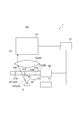
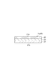
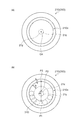
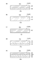
- FIG. 3 It is the figure which showed typically the structure of the measuring apparatus which concerns on embodiment of this invention. It is a top view of the shielding board in the measuring apparatus of FIG. 3 is a cross-sectional view taken along line III-III in FIG. It is a bottom view of the shielding board concerning a modification. It is a bottom view of the shielding board concerning a modification. It is a bottom view of the shielding board concerning a modification. It is sectional drawing of the shielding board which concerns on a modification.
- the measuring apparatus 1 is a micro-optical system that measures the temperature of a semiconductor device D, which is a device under test (DUT) (measurement target), in a non-contact manner.
- System System
- the measuring apparatus 1 measures the temperature of the semiconductor device D in a non-contact manner by performing heat generation observation in a state where the emissivity of the semiconductor device D is unknown.
- an integrated circuit having a PN junction such as a transistor (for example, a small scale integrated circuit (SSI), a medium scale integrated circuit (MSI), a large scale integrated circuit (LSI: Large)).
- Scale Integration Very Large Scale Integration (VLSI), Ultra Large Scale Integration (ULSI), Giga Scale Integration (GSI), High Current / High Voltage MOS transistors, bipolar transistors, and power semiconductor elements (power devices).
- the semiconductor device D is placed on, for example, a sample stage (not shown).
- the measurement target is not limited to a semiconductor device, and various devices such as a solar cell module such as a solar cell panel can be measured.
- the measuring apparatus 1 has a tester unit 11 (signal input unit), an objective lens 12 (light guide optical system), and an infrared camera 13 (imaging unit, infrared detector) as a functional configuration related to temperature measurement of the semiconductor device D. And a computer 14 (arithmetic unit), a shielding plate 20, and a temperature controller 28 (temperature control unit).
- the tester unit 11 is electrically connected to the semiconductor device D via a cable and functions as a signal input unit that applies a measurement signal to the semiconductor device D.
- the tester unit 11 is operated by a power source (not shown), and repeatedly applies a signal for driving the semiconductor device D, a clock signal, and the like as a measurement signal.
- the tester unit 11 may apply a modulation current signal, or may apply a CW (continuous wave) current signal.
- the tester unit 11 is electrically connected to the computer 14 via a cable, and applies a signal designated by the computer 14 to the semiconductor device D. Note that the tester unit 11 does not necessarily have to be electrically connected to the computer 14. When the tester unit 11 is not electrically connected to the computer 14, the tester unit 11 determines a signal alone and applies the signal to the semiconductor device D.
- the shielding plate 20 is a member used for non-contact measurement of the temperature of the semiconductor device D.
- the shielding plate 20 is disposed between the semiconductor device D and the objective lens 12, and more specifically, is provided so that the central shielding portion 21 z is positioned on the optical axis OA of the objective lens 12.
- the shielding plate 20 includes a base material 21 whose temperature can be adjusted according to control by the temperature controller 28.
- the base material 21 a member having high thermal conductivity and characteristics as a black body or a reflective material may be used.
- the base material 21 may have a structure in which a fluid flows inside, a heating wire, or the like.
- the base material 21 may include a heat pipe, a rubber heater, or the like.
- the base material 21 has a three-layer structure in which a substrate layer 23, a black body layer 24 (first layer), and a reflective layer 22 (second layer) are laminated. Yes.
- the substrate layer 23 conducts heat according to control by the temperature controller 28.
- the substrate layer 23 is provided so as to be sandwiched between the black body layer 24 and the reflective layer 22. Therefore, the substrate layer 23 and the black body layer 24 and the substrate layer 23 and the reflective layer 22 are thermally connected to each other.
- a member having high thermal conductivity capable of realizing a uniform temperature for example, copper (a copper plate or a copper layer) can be used.
- the substrate layer 23 may have a structure in which fluid flows inside, a heating wire, or the like.
- the base material 21 may include a heat pipe, a rubber heater, or the like.
- the black body layer 24 has a black body surface 21b (black body portion) on the surface (outer surface) opposite to the surface in contact with the substrate layer 23.
- the black body surface 21 b is a surface on one side of the base material 21 in the stacking direction.
- the black body surface 21 b faces the semiconductor device D.
- the black body layer 24 is subjected to, for example, a Raydent (registered trademark) process, and has a higher emissivity and a lower reflectivity than the reflective layer 22, that is, a large amount of heat radiation. Thereby, at least a part of the black body surface 21b is in a black body state with respect to infrared rays.
- the amount of heat radiation of the black body surface 21b in the black body state is that of the reflective surface 21a (details will be described later) on the opposite side of the black body surface 21b in the base material 21, that is, the other side in the stacking direction of the base material 21 Greater than thermal radiation.
- a black ceramic film can be used as the black body layer 24 for example.
- a black body refers to an object (complete black body) that can completely absorb electromagnetic waves incident from the outside over all wavelengths and can radiate heat.
- the black body state in this embodiment is like this. This is a state in which a complete black body is not shown, and at least the heat radiation equivalent to that of a black body can be realized for infrared rays.
- the state where heat radiation equivalent to that of a black body can be realized refers to a state where the emissivity is 90% or more, for example.
- the reflective layer 22 has a reflective surface 21 a on the surface (outer surface) opposite to the surface in contact with the substrate layer 23. That is, the reflective layer 22 is provided so as to sandwich the substrate layer 23 between the black body layer 24.
- the reflecting surface 21 a faces the objective lens 12. That is, the reflective surface 21a is a surface located on the opposite side of the black body surface 21b in the base material 21.
- a member that increases the reflectance of the reflection surface 21a at the detection wavelength of the infrared camera 13, for example, gold plating can be used.
- the reflective surface 21a is a mirror surface due to a high reflectance (for example, 90% or more). For this reason, the infrared camera 13 is in a narcissus state (a state in which it is seen). Thereby, it is possible to prevent the dark level of the infrared camera 13 from changing according to the change in the temperature of the base material 21 and to improve the SN.
- the base material 21 has a central shielding part 21z (shielding part) formed around the central axis CA of the shielding plate 20 on the black body surface 21b.
- the central shielding part 21z is formed in the range of a circumscribed circle 21y of the effective visual field 21x corresponding to the imaging part 10 (including at least the infrared camera 13 and the objective lens 12) with at least the central axis CA as a center.
- the size of the effective visual field 21x corresponding to the imaging unit 10 is determined by the performance and arrangement relationship of the objective lens 12 and the infrared camera 13 included in the imaging unit 10.
- the temperature is derived by detecting the heat ray including the heat ray emitted from the semiconductor device D and the heat ray reflected by the semiconductor device D by the infrared camera 13. Is done.
- the heat ray reflected in the semiconductor device D is a heat ray reflected by the semiconductor device D according to the heat ray irradiated to the semiconductor device D from the black body surface 21b. If the central shielding part 21z is not provided and the range of the central axis CA in the base material 21 is an opening, the black body is not provided immediately above the semiconductor device D on the central axis CA. Become.
- the heat rays on the central axis CA the heat rays reflected by the semiconductor device D according to the heat rays irradiated to the semiconductor device D from the black body surface 21b described above do not exist. Therefore, the heat ray that passes through the central axis CA and is detected by the infrared camera 13 is only the heat ray emitted from the semiconductor device D, and there is a possibility that the temperature cannot be appropriately measured by the above-described temperature deriving method. In this respect, by providing the central shielding portion 21z, it is possible to prevent only the heat rays emitted from the semiconductor device D from being detected by the infrared camera 13.
- the base material 21 has an opening 21c formed around the central shielding part 21z. More specifically, the opening 21c is formed in a semicircular shape in a bottom view so as to be adjacent to the circumscribed circle 21y on the black body surface 21b. Only one opening 21c is formed around the central shielding part 21z so as to be rotationally symmetric about the central shielding part 21z. The opening 21c is formed so as to penetrate the base material 21 from the black body surface 21b side to the reflecting surface 21a side (see FIG. 1). The opening 21c is formed such that the opening shape gradually decreases from the black body surface 21b side to the reflecting surface 21a side.
- the inner peripheral surface 21d of the opening 21c that divides the region of the opening 21c has an oblique structure so as to approach the central portion of the opening 21c from the black body surface 21b toward the reflecting surface 21a. (See FIG. 1).
- the inner peripheral surface 21d is subjected to a rayent (registered trademark) process or the like and is in a black body state.
- the oblique structure of the inner peripheral surface 21d is determined in consideration of the viewing angle of the lens of the infrared camera 13 so that the inner peripheral surface 21d cannot be observed from the infrared camera 13. Since the inner peripheral surface 21d has such an oblique structure, only the heat rays generated from the semiconductor device D can be prevented from being reflected by the inner peripheral surface 21d and detected by the infrared camera 13.
- the base material 21 has a black body state opposing shielding part 21e (black body part) formed on the black body surface 21b so as to face the opening 21c with the central shielding part 21z interposed therebetween. More specifically, the opposing shielding part 21e is formed so as to include a region facing the opening 21c with the central axis CA as a center.
- the size (area) of the opposing shielding part 21e may be smaller than the size (area) of the opening 21c in the black body surface 21b.
- the shape and size of the opposing shielding portion 21e may substantially match the shape and size of the opening 21c in the black body surface 21b.
- the semiconductor device D is irradiated with heat rays x1 from the opposing shielding portion 21e in a black body state.
- the heat ray x21 is reflected according to the heat ray x1.
- the said heat ray x21 reaches
- the heat ray x22 generated in the semiconductor device D reaches the opening 21c. That is, the heat ray x2 including the heat ray x21 reflected in the semiconductor device D and the heat ray x22 generated in the semiconductor device D reaches the opening 21c.
- the heat ray x ⁇ b> 2 passes through the opening 21 c and is detected by the infrared camera 13 through the objective lens 12.
- the heat rays detected by the infrared camera 13 may be almost all heat rays x2. That is, the heat ray reflected by the semiconductor device D detected by the infrared camera 13 corresponds to the semiconductor device D according to the heat ray irradiated to the semiconductor device D from the opposing shielding portion 21e which is a black body surface. May be the reflected heat ray x21.
- the effective visual field 21x corresponding to the imaging unit 10 is not taken into consideration, that is, when the size of the effective visual field 21x corresponding to the imaging unit 10 is assumed to be 0, an infrared camera is provided by providing the above-described opposing shielding unit 21e.
- All the heat rays reflected by the semiconductor device D detected by 13 can be set as the heat rays x21.
- the infrared camera 13 detects the heat rays reflected by the semiconductor device D other than the heat ray x21 according to the size of the effective visual field 21x corresponding to the imaging unit 10.
- the infrared camera 13 has a region (hereinafter referred to as a peripheral region) between the outer edge of the region of the opposing shielding part 21e and a position outside the outer edge by the diameter of the circumscribed circle 21y of the effective visual field 21x.
- the heat ray reflected by the semiconductor device D is detected according to the heat ray irradiated to the semiconductor device D.
- the peripheral shielding portion 31 black body portion that is in a black body state is provided in the peripheral region described above so as to surround the outer edge of the opposing shielding portion 21e.
- the peripheral shielding unit 31 is provided in an area defined according to an effective visual field corresponding to the imaging unit 10. More specifically, the peripheral shielding unit 31 is provided in a region defined by a trajectory that circles the circumscribed circle 21y of the effective visual field 21x corresponding to the imaging unit 10 with respect to the opposing shielding unit 21e.
- the temperature controller 28 is a temperature control unit that controls the temperature of the shielding plate 20.
- the temperature controller 28 is a temperature controller such as a heater or a cooler that is thermally connected to the shielding plate 20 and conducts heat to the shielding plate 20 to control the temperature of the shielding plate 20.
- the temperature controller 28 controls the temperature of the shielding plate 20 according to the setting from the computer 14. For example, the temperature controller 28 may control the temperature of the shielding plate 20 by conducting heat to the shielding plate 20 (base material 21) with a liquid or a heating wire.
- the objective lens 12 is a light guide optical system that guides the heat ray x2 that has passed through the opening 21c of the shielding plate 20 to the infrared camera 13.
- the objective lens 12 is provided such that its optical axis coincides with the optical axis OA.
- the infrared camera 13 is an infrared detector that captures an image of the heat ray x2 emitted from the semiconductor device D driven in accordance with the input of the measurement signal through the objective lens 12.
- the infrared camera 13 has a light receiving surface on which a plurality of pixels that convert infrared rays into electrical signals are two-dimensionally arranged.
- the infrared camera 13 captures heat rays to generate an infrared image (thermal image data (detection signal)) and outputs the infrared image to the computer 14.
- a two-dimensional infrared detector such as an InSb camera is used.
- the infrared detector is not limited to a two-dimensional infrared detector, and a one-dimensional infrared detector such as a bolometer or a point infrared detector may be used.
- electromagnetic waves (light) having a wavelength of 0.7 ⁇ m to 1000 ⁇ m are called infrared rays.
- electromagnetic waves (light) in the mid-infrared to far-infrared region having a wavelength of 2 ⁇ m to 1000 ⁇ m are referred to as heat rays.
- the computer 14 is electrically connected to the infrared camera 13.
- the calculator 14 derives the temperature of the semiconductor device D based on the infrared image generated by the infrared camera 13.
- the calculator 14 has a processor that performs a function of deriving the temperature of the semiconductor device D.
- a derivation principle of temperature derivation based on an infrared image will be described.
- an area 1 which is an area having a constant emissivity and an area 2 which is another area having an emissivity lower than that of the area 1 are in the vicinity.
- the emissivity and reflectance of each area are ⁇ 1 , ⁇ 1 , ⁇ 2 , and ⁇ 2 .
- the following equations (1) and (2) are established according to Kirchhoff's law.
- area 1 having an emissivity of ⁇ 1 may be described as a high emissivity portion
- area 2 having an emissivity of ⁇ 2 may be described as a low emissivity portion.
- the thermal radiance (thermal radiation amount) of the shielding plate 20 is L low
- the radiation detected by the infrared camera 13 for the high emissivity part is S 1low
- the infrared camera 13 detects the radiation detected for the low emissivity part
- S 1low can be rephrased as thermal radiance in the high emissivity part
- S 2low can be restated as thermal radiance in the low emissivity part.
- the following equation (3) indicates that the semiconductor device D emitted from the high emissivity portion of the semiconductor device D is generated in the infrared camera 13 when the thermal radiance of the shielding plate 20 is L low. It shows that a heat ray having a thermal radiance S1low in which a heat ray and a heat ray reflected by the semiconductor device D are superimposed is detected. Further, the following equation (4) indicates that when the thermal radiance of the shielding plate 20 is L low , the semiconductor device D radiated from the low emissivity portion of the semiconductor device D is generated in the infrared camera 13. It shows that a heat ray having a thermal radiance of S 2low in which a heat ray and a heat ray reflected by the semiconductor device D are superimposed is detected.
- the ratio R of the reflectance of the high emissivity part and the low emissivity part is expressed by the following expression (7) from the above expressions (3) to (6).
- the following expression (8) is derived from the above expressions (3), (4), and (7).
- the following expression (9) is derived from the above-described expressions (5), (6), and (7).
- the semiconductor device D is placed on the sample stage (not shown) of the measuring apparatus 1.
- a tester unit 11 is electrically connected to the semiconductor device D, and signals for driving the semiconductor device D and measurement signals such as a clock signal are input from the tester unit 11.
- the temperature of the shielding plate 20 is controlled by the temperature controller 28 so that the black body surface 21b of the shielding plate 20, more specifically, the thermal radiance of the opposing shielding portion 21e becomes L low .
- the semiconductor device D is irradiated with heat rays having a thermal radiance of L low from the shielding plate 20.
- a heat ray including the heat ray generated by the semiconductor device D and the heat ray reflected by the semiconductor device D in response to the heat ray from the shielding plate 20 passes through the opening 21c of the shielding plate 20 and the objective lens 12, and is infrared. It is detected by the camera 13.
- the infrared camera 13 captures the heat ray and generates an infrared image.
- the infrared image includes radiation of two areas having different emissivities, that is, a high emissivity part and a low emissivity part.
- the computer 14 from the infrared image identifies the radiation S 2Low radiation S 1Low and low emissivity of the high emissivity unit.
- the temperature of the shielding plate 20 is controlled by the temperature controller 28 so that the black body surface 21b of the shielding plate 20, more specifically, the thermal radiance of the opposing shielding portion 21e becomes L high .
- the semiconductor device D is irradiated with heat rays having a thermal radiance L high from the shielding plate 20.
- a heat ray including the heat ray generated by the semiconductor device D and the heat ray reflected by the semiconductor device D in response to the heat ray from the shielding plate 20 passes through the opening 21c of the shielding plate 20 and the objective lens 12, and is infrared. It is detected by the camera 13.
- the infrared camera 13 captures the heat ray and generates an infrared image.
- the infrared image includes radiation of two areas having different emissivities, that is, a high emissivity part and a low emissivity part.
- the calculator 14 specifies the radiation S 1high of the high emissivity part and the radiation S 2high of the low emissivity part from the infrared image.
- the temperature of the semiconductor device D is derived from the radiation S 1high and the radiation S 2high of the low emissivity part.
- the temperature measurement procedure of the semiconductor device D has been described above, but the temperature measurement using the present invention is not limited to the above procedure.
- the temperature of the shielding plate 20 is changed by the temperature controller 28 so that the thermal radiance becomes a temperature from L low to L high , but another shielding plate different from the shielding plate 20 is prepared, The shield plate 20 may be replaced.
- the thermal radiation amount of the semiconductor device D can be changed by setting the thermal radiance of the shielding plate 20 to L high and the thermal radiance to L low .
- a sample coated with a metal having a very high emissivity for example, gold or aluminum
- the zero point correction of the infrared camera 13 may be performed by detecting the dark state without the heat ray emitted from the sample by the infrared camera 13.
- the central axis of the shielding plate 20 is covered with the central shielding portion 21z.
- the central shielding portion 21z is disposed immediately above the semiconductor device D.
- the portion directly above the semiconductor device D is not shielded, only the heat rays generated by the semiconductor device D may be transmitted to the infrared camera 13 from the unshielded portion. It is not preferable in securing.
- the central shielding portion 21z immediately above the semiconductor device D it is possible to suppress only the heat rays generated by the semiconductor device D from being transmitted to the infrared camera 13.
- an opening 21c is formed around the center shielding part 21z, and a black body state opposing shielding part 21e is formed so as to face the opening 21c with the center shielding part 21z interposed therebetween. Since the opening portion 21c and the opposing shielding portion 21e are formed to face each other, the heat rays applied to the semiconductor device D from the opposing shielding portion 21e on the black body surface 21b that is an auxiliary heat source are reflected by the semiconductor device D and are opened. It passes through the part 21c and reaches the infrared camera 13. Further, the heat rays generated by the semiconductor device D also pass through the opening 21c and reach the infrared camera 13.
- the infrared rays are detected by the infrared camera 13 including the heat rays generated by the semiconductor device D and the heat rays reflected by the semiconductor device D.
- the semiconductor device D is generated by the opening 21c and the opposing shielding portion 21e.
- a heat ray including a heat ray and a heat ray reflected by the semiconductor device D is detected by the infrared camera 13.
- the surface temperature of the measurement object can be measured with high accuracy in a non-contact manner in a micro optical system.
- the base material 21 further includes a black body-state peripheral shielding part 31 that surrounds the outer edge of the opposing shielding part 21e.
- the peripheral shielding part 31 is defined according to the size of the effective field of view according to the imaging unit 10. It is considered to be an area.
- the infrared camera 13 may capture only the heat rays including the heat rays generated by the semiconductor device D and the heat rays reflected by the semiconductor device D.
- the heat ray reflected in the semiconductor device D may be a heat ray reflected in the semiconductor device D according to the heat ray from the surface (for example, the opposing shielding part 21e) made into the black body state.
- the heat rays reflected by the semiconductor device D captured by the infrared camera 13 are opposite to each other. Only the heat rays reflected from the semiconductor device D according to the heat rays irradiated to the semiconductor device D from the shielding part 21e are provided. However, actually, the heat ray reflected from the semiconductor device D according to the heat ray irradiated to the semiconductor device D from the region outside the opposing shielding portion 21e only in the region corresponding to the size of the effective visual field corresponding to the imaging unit 10 Also, the infrared camera 13 takes an image.
- the heat rays reflected by the semiconductor device D are It can be set as the heat ray reflected by the semiconductor device D according to the heat ray from the surface made into the black body state, and measurement accuracy can be ensured.
- the peripheral shielding part 31 is provided in an area defined by a locus in which a circumscribed circle 21y having an effective field of view corresponding to the imaging part 10 is circulated with respect to the opposing shielding part 21e.
- the measuring apparatus 1 is a measuring apparatus that measures the temperature of the semiconductor device D in a non-contact manner, and includes the shielding plate 20 described above, a temperature controller 28 that controls the temperature of the shielding plate 20 in an adjustable manner, and the semiconductor device D. And a tester unit 11 for inputting a measurement signal, and an infrared camera 13 for imaging a heat ray from the semiconductor device D in response to the input of the measurement signal.
- the central axis of the shielding plate 20 on the black body surface 21b is covered with the central shielding portion 21z in the black body state.
- the shielding plate 20 is provided so that the central axis thereof coincides with the optical axis OA of the heat ray from the semiconductor device D toward the infrared camera 13.
- the central shielding part 21z is disposed immediately above the semiconductor device D.
- the portion directly above the semiconductor device D is not shielded, only the heat rays generated by the semiconductor device D may be transmitted to the infrared camera 13 from the unshielded portion.
- the central shielding portion 21z immediately above the semiconductor device D it is possible to suppress only the heat rays generated by the semiconductor device D from being transmitted to the infrared camera 13.
- an opening 21c is formed around the center shielding portion 21z, and a black body-state facing shielding portion 21e is formed so as to face the opening 21c with the center shielding portion 21z interposed therebetween. ing. Since the opening portion 21c and the opposing shielding portion 21e are formed to face each other, the heat rays applied to the semiconductor device D from the opposing shielding portion 21e on the black body surface 21b that is an auxiliary heat source are reflected by the semiconductor device D and are opened. It passes through the part 21c and reaches the infrared camera 13. Further, the heat rays generated by the semiconductor device D also pass through the opening 21c and reach the infrared camera 13.
- the infrared rays are detected by the infrared camera 13 including the heat rays generated by the semiconductor device D and the heat rays reflected by the semiconductor device D. That is, for example, when a measurement signal is input from the tester unit 11 to the semiconductor device D and the semiconductor device D is driven, the semiconductor device D is irradiated with heat rays from the opposing shielding portion 21e of the black body surface 21b, and the semiconductor device D is driven. A heat ray including a heat ray reflected by the device D and a heat ray generated by the semiconductor device D is detected by the infrared camera 13.
- the temperature of the base material 21 of the shielding plate 20 is adjusted by the temperature controller 28.
- the infrared camera 13 can detect the heat rays including the heat rays reflected by the semiconductor device D and the heat rays generated by the semiconductor device D while changing the temperature of the black body surface 21b which is an auxiliary heat source.
- the surface temperature of the semiconductor device D whose emissivity is unknown can be measured with high accuracy in a non-contact manner.
- only the heat rays generated by the semiconductor device D are suppressed from being captured by the infrared camera 13 by the central shielding portion 21z, and the semiconductor device D is generated by the opening 21c and the opposing shielding portion 21e.
- the heat ray including the heat ray and the heat ray reflected by the semiconductor device D is imaged by the infrared camera 13, it is possible to measure the surface temperature of the measurement object with high accuracy in a non-contact manner in the micro optical system. it can.
- this invention is not limited to the said 1st Embodiment.
- one opening 21c is formed in the shielding plate 20 so as to be rotationally symmetric about the center shielding part 21z
- the opening is not limited to this, and the opening is center shielded. It may be formed around the central shielding part 21z so as to be an odd number of rotational symmetry around the part 21z. By providing the opening so as to be odd-numbered rotationally symmetric, the opening and the opposing shielding portion can be surely opposed to each other.
- the opening is formed in a rotationally symmetrical manner, the thermal conductivity of the shielding plate is improved, and the temperature uniformity of the shielding plate can be improved.
- the opening portion is provided so as to be rotationally symmetrical an odd number will be described with reference to FIGS. 4 and 5.
- the opening 21Ac is formed around the central shielding part 21z so as to be three-fold rotationally symmetric about the central shielding part 21z.
- the opening 21Ac has a fan shape and is formed around the center shielding part 21z at equal intervals.
- an opposing shielding portion 21Ae in a black body state is provided so as to face the opening portion 21Ac with the central axis CA as a center.
- the shape and size of the opposing shielding portion 21Ae substantially match the shape and size of the opening 21Ac on the black body surface.
- a peripheral region that is a region between the outer edge of the region of the opposing shielding portion 21Ae and a position outside the outer edge by the diameter of the circumscribed circle 21y of the effective visual field 21x surrounds the outer edge of the opposing shielding portion 21Ae.
- the peripheral shielding portion 31A in the black body state is provided in the same manner as the opposing shielding portion 21Ae.
- the opening 21Bc is formed around the central shielding part 21z so as to be five-fold rotationally symmetric about the central shielding part 21z.
- the openings 21Bc are fan-shaped, and five openings are formed at equal intervals around the central shielding part 21z.
- the opposing shielding portion 21Be in a black body state is provided so as to face the opening 21Bc with the central axis CA as a center.
- the shape and size of the opposing shielding portion 21Be substantially match the shape and size of the opening 21Bc on the black body surface.
- a peripheral region that is a region between the outer edge of the area of the opposing shielding portion 21Be and a position outside the outer edge by the diameter of the circumscribed circle 21y of the effective visual field 21x is surrounded by the outer edge of the opposing shielding portion 21Be.
- a black body state peripheral shielding part 31B is provided similarly to the opposing shielding part 21Be.
- the opening 21Dc may be formed in an annular shape around the opposing shielding part 31D (black body part).
- a central shielding part 21z in a black body state is formed so as to cover the central axis CA.
- the central shielding part 21z is formed in a range of a circumscribed circle 21y of the effective visual field 21x of the imaging unit 10 with the central axis CA as the center.
- the opening 21Dc is formed at a position 6r from a position 5r from the center of the circumscribed circle 21y. That is, the opening width of the annular opening 21Dc is r.
- a black body-state opposing shielding part 31D is provided in a region between the inner edge of the opening 21Dc and a position inside the inner edge by a diameter (2r) of the circumscribed circle 21y.
- the opposing shielding part 31D functions as a black body part. That is, the opposing shielding part 31D is formed on the black body surface so as to face the opening part 21Dc with the region closer to the opening part 21Dc than the center of the center shielding part 21z.
- the shielding point P1 which is one point of the opposing shielding part 31D, is centered on a central point P2 that is a point on the opening part 21Dc side opposite to the center of the central shielding part 21z in the central shielding part 21z.
- the lens between the infrared camera and the measurement target Only a part of the bias is used, and image flow may be a problem in an image based on heat rays detected by an infrared camera.
- image flow becomes a problem for example, the heat ray may be detected by an infrared camera while appropriately rotating the shielding plate around the central axis CA. By doing so, temperature measurement can be performed while avoiding the use of only a part of the lens.
- the heat ray is detected a plurality of times with an infrared camera while rotating at least once (360 degrees), and images based on the plurality of heat rays are integrated.
- the image flow may be reduced (if the shielding plate 20A is three-fold rotationally symmetric shown in FIG. 4, it is rotated at least 1/3 (120 degrees), and the five-fold rotationally symmetric shown in FIG. If it is the shielding plate 20B, it is rotated at least 1/5 (72 degrees).
- the shielding plate 20D in which the opening 21Dc is formed in an annular shape a heat ray that has passed through the annular opening 21Dc is detected by the infrared camera, so that one of the lenses between the infrared camera and the measurement object is detected. Since only the portion is not used, the above-described image flow hardly occurs, and measurement can be performed without rotating the shielding plate.
- the shielding plate 20 is described as having a three-layer structure in which the substrate layer 23, the black body layer 24, and the reflection layer 22 are stacked, and the substrate layer 23 is described as being, for example, copper (copper plate or copper layer).
- the base material 81 includes a substrate layer 83, a black body layer 84 having the black body surface 84 x as an outer surface, and a substrate between the black body layer 84.
- a heat insulating material 83a provided so as to sandwich the layer 83, and a reflective layer 82 provided so as to sandwich the heat insulating material 83a between the substrate layer 83 and having the reflective surface 82x as an outer surface.
- the heat insulating material 83 a is provided between the substrate layer 83 and the reflective layer 82, the heat conduction amount from the substrate layer 83 to the reflective layer 82 rather than the heat conduction amount from the substrate layer 83 to the black body layer 84. Can be reduced. Thereby, the heat radiation amount of the black body surface can be easily made larger than the heat radiation amount of the reflection surface.
- a heat insulating layer may be formed by providing a vacuum layer between the substrate layer 83 and the reflective layer 82 instead of the heat insulating material 83a.
- the base material of the shielding plate may have a two-layer structure.
- the substrate 41 of the shielding plate 40 in FIG. 7A includes a substrate layer 42 having the reflective surface 42x as an outer surface, and a black body layer 43 having a black body surface 43x as an outer surface provided so as to overlap the substrate layer 42. ,have.
- the amount of heat radiation of the black body layer 43 is made larger than the amount of heat radiation of the substrate layer 42. Thereby, the heat radiation amount of the black body surface 43x and the heat radiation amount of the reflection surface 42x can be easily made different.
- the base material 41 since the base material 41 has a two-layer structure, it is easy to create a shielding plate.
- the substrate layer 42 for example, copper (copper plate or copper layer) or gold (gold plate or gold layer) can be used.
- the black body layer 43 for example, a black ceramic film can be used as the black body layer 43 .
- the substrate 51 of the shielding plate 50 in FIG. 7B includes a substrate layer 53 having a black body surface 53x as an outer surface, a reflective layer 52 having an outer surface as a reflecting surface 52x, and provided so as to overlap the substrate layer 53. have.
- the amount of heat radiation of the reflective layer 52 is smaller than the amount of heat radiation of the substrate layer 53. Thereby, the heat radiation amount of the black body surface 53x and the heat radiation amount of the reflection surface 52x can be easily made different. Further, since the base material 51 has a two-layer structure, it is easy to create a shielding plate.
- the substrate layer 53 for example, carbon or graphene can be used.
- the reflective layer 52 for example, gold plating can be used.
- the shielding plate may be composed only of the substrate layer.
- the base material 61 of the shielding plate 60 in FIG. 7C has a substrate layer 62 having the reflection surface 62x as an outer surface.
- the surface opposite to the reflecting surface 62x is made a black body surface 63 by the blackening process.
- the black body surface is formed by processing the substrate layer having the reflective surface, so that the shielding plate can be easily created and the number of components can be reduced.
- gold can be used as the substrate layer 62.
- the black body surface 63 subjected to the blackening process is blackened gold.
- the base 71 of the shielding plate 70 has a three-layer structure, a substrate layer 73 having a thermoelectric element, a black body layer 74 having a black body surface 74x as an outer surface, A reflective layer 72 having the reflective surface 72x as an outer surface may be laminated.
- the thermoelectric element is, for example, a Peltier element, Seebeck element, or Thomson element.
- the black body layer 74 for example, a black ceramic coating can be used.
- the reflective layer 72 for example, gold plating can be used.
- the substrate layer 73 absorbs heat at the junction with the reflective layer 72 that is gold plating when a current or voltage is applied, and a black body layer that is a black ceramic film. Heat is generated at the junction with 74. As a result, the amount of radiant heat on the black body surface of the black body layer 74 is greater than the amount of radiant heat on the reflective surface of the reflective layer 72.
- a temperature controller temperature control part
- the substrate layer 73 which has a thermoelectric element a temperature controller (temperature control part) is electrically connected with a thermoelectric element, and controls the temperature of the shielding board 70 by applying an electric current or a voltage. Thereby, the temperature of the shielding plate having the thermoelectric element can be controlled easily and reliably.
- the center shielding part 21z demonstrated that it was a black body state, it is not limited to this, At least the opposing shielding part (black body part) formed so as to oppose an opening part among black body surfaces is infrared rays. On the other hand, it is only necessary to be in a black body state, and the central shielding portion is not necessarily in the black body state.
- SYMBOLS 1 DESCRIPTION OF SYMBOLS 1 ... Measuring apparatus, 11 ... Tester unit (signal input part), 12 ... Objective lens (imaging part, light guide optical system), 13 ... Infrared camera (imaging part, infrared detector), 14 ... Calculator (calculation part) 20, 20A, 20B, 20D, 40, 50, 60, 70, 80 ... shielding plate, 21, 21A, 21B, 21D, 41, 51, 61, 71, 81 ... base material, 21c, 21Ac, 21Bc, 21Dc ... Opening part, 21e, 21Ae, 21Be, 31D ... Opposing shielding part (black body part), 21a, 42x, 52x, 62x ...
Landscapes
- Physics & Mathematics (AREA)
- General Physics & Mathematics (AREA)
- Spectroscopy & Molecular Physics (AREA)
- Radiation Pyrometers (AREA)
- Geophysics And Detection Of Objects (AREA)
Abstract
Priority Applications (4)
| Application Number | Priority Date | Filing Date | Title |
|---|---|---|---|
| CN201680030362.2A CN107615024A (zh) | 2015-05-27 | 2016-05-24 | 屏蔽板以及测定装置 |
| KR1020177023403A KR20180011752A (ko) | 2015-05-27 | 2016-05-24 | 차폐판 및 측정 장치 |
| US15/559,430 US20180080831A1 (en) | 2015-05-27 | 2016-05-24 | Shield plate and measurement apparatus |
| DE112016002372.3T DE112016002372T5 (de) | 2015-05-27 | 2016-05-24 | Abschirmplatte und Messvorrichtung |
Applications Claiming Priority (2)
| Application Number | Priority Date | Filing Date | Title |
|---|---|---|---|
| JP2015107800A JP2016223811A (ja) | 2015-05-27 | 2015-05-27 | 遮蔽板及び測定装置 |
| JP2015-107800 | 2015-05-27 |
Publications (1)
| Publication Number | Publication Date |
|---|---|
| WO2016190298A1 true WO2016190298A1 (fr) | 2016-12-01 |
Family
ID=57392807
Family Applications (1)
| Application Number | Title | Priority Date | Filing Date |
|---|---|---|---|
| PCT/JP2016/065278 Ceased WO2016190298A1 (fr) | 2015-05-27 | 2016-05-24 | Plaque de protection et dispositif de mesure |
Country Status (6)
| Country | Link |
|---|---|
| US (1) | US20180080831A1 (fr) |
| JP (1) | JP2016223811A (fr) |
| KR (1) | KR20180011752A (fr) |
| CN (1) | CN107615024A (fr) |
| DE (1) | DE112016002372T5 (fr) |
| WO (1) | WO2016190298A1 (fr) |
Cited By (1)
| Publication number | Priority date | Publication date | Assignee | Title |
|---|---|---|---|---|
| EP3421954A3 (fr) * | 2017-06-28 | 2019-02-20 | MBDA Deutschland GmbH | Dispositif de compensation destiné à la mise en uvre d'une compensation des irrégularités d'un détecteur infrarouge dans un autodirecteur d'un missile guidé, autodirecteur et procédé de mise en uvre d'une compensation des irrégularités |
Families Citing this family (5)
| Publication number | Priority date | Publication date | Assignee | Title |
|---|---|---|---|---|
| US12230521B2 (en) | 2019-06-03 | 2025-02-18 | Applied Materials, Inc. | Method for non-contact low substrate temperature measurement |
| CN111780879B (zh) * | 2020-07-22 | 2021-07-02 | 武汉博宇光电系统有限责任公司 | 一种红外测温系统及测温方法 |
| CZ2020582A3 (cs) * | 2020-10-27 | 2022-04-13 | Západočeská Univerzita V Plzni | Způsob kontroly svarů, zejména bodových |
| CN114323309B (zh) * | 2021-12-22 | 2024-11-15 | 北京星航机电装备有限公司 | 一种红外辐射遮挡装置、红外探测器标定方法及自检方法 |
| KR102712905B1 (ko) * | 2022-06-13 | 2024-10-07 | 주식회사 티마트 | 비접촉 온도 측정장치 |
Citations (4)
| Publication number | Priority date | Publication date | Assignee | Title |
|---|---|---|---|---|
| JPS4733722Y1 (fr) * | 1968-02-15 | 1972-10-12 | ||
| JPS5858427A (ja) * | 1981-10-02 | 1983-04-07 | Matsushita Electric Ind Co Ltd | 赤外線放射温度計測装置 |
| JPH05346351A (ja) * | 1992-06-16 | 1993-12-27 | Tokai Carbon Co Ltd | 放射測温装置および放射測温法 |
| US20140314118A1 (en) * | 2013-04-19 | 2014-10-23 | Joseph D. LaVeigne | Blackbody function |
Family Cites Families (6)
| Publication number | Priority date | Publication date | Assignee | Title |
|---|---|---|---|---|
| US2611541A (en) * | 1950-02-07 | 1952-09-23 | Leeds & Northrup Co | Radiation pyrometer with illuminator |
| US4776825A (en) * | 1987-05-22 | 1988-10-11 | Beckman Instruments, Inc. | Differential temperature measuring radiometer |
| US6232614B1 (en) * | 1998-10-13 | 2001-05-15 | James W. Christy | Low-temperature blackbody radiation source |
| JP4567806B1 (ja) * | 2010-01-08 | 2010-10-20 | 立山科学工業株式会社 | 非接触温度センサ |
| CN201653554U (zh) * | 2010-02-23 | 2010-11-24 | 宝山钢铁股份有限公司 | 红外热像仪校正装置 |
| US9689746B2 (en) * | 2010-12-13 | 2017-06-27 | National Institute Of Advanced Industrial Science And Technology | Method and system of measuring surface temperature |
-
2015
- 2015-05-27 JP JP2015107800A patent/JP2016223811A/ja active Pending
-
2016
- 2016-05-24 DE DE112016002372.3T patent/DE112016002372T5/de not_active Withdrawn
- 2016-05-24 WO PCT/JP2016/065278 patent/WO2016190298A1/fr not_active Ceased
- 2016-05-24 CN CN201680030362.2A patent/CN107615024A/zh active Pending
- 2016-05-24 KR KR1020177023403A patent/KR20180011752A/ko not_active Withdrawn
- 2016-05-24 US US15/559,430 patent/US20180080831A1/en not_active Abandoned
Patent Citations (4)
| Publication number | Priority date | Publication date | Assignee | Title |
|---|---|---|---|---|
| JPS4733722Y1 (fr) * | 1968-02-15 | 1972-10-12 | ||
| JPS5858427A (ja) * | 1981-10-02 | 1983-04-07 | Matsushita Electric Ind Co Ltd | 赤外線放射温度計測装置 |
| JPH05346351A (ja) * | 1992-06-16 | 1993-12-27 | Tokai Carbon Co Ltd | 放射測温装置および放射測温法 |
| US20140314118A1 (en) * | 2013-04-19 | 2014-10-23 | Joseph D. LaVeigne | Blackbody function |
Cited By (1)
| Publication number | Priority date | Publication date | Assignee | Title |
|---|---|---|---|---|
| EP3421954A3 (fr) * | 2017-06-28 | 2019-02-20 | MBDA Deutschland GmbH | Dispositif de compensation destiné à la mise en uvre d'une compensation des irrégularités d'un détecteur infrarouge dans un autodirecteur d'un missile guidé, autodirecteur et procédé de mise en uvre d'une compensation des irrégularités |
Also Published As
| Publication number | Publication date |
|---|---|
| DE112016002372T5 (de) | 2018-02-15 |
| JP2016223811A (ja) | 2016-12-28 |
| US20180080831A1 (en) | 2018-03-22 |
| KR20180011752A (ko) | 2018-02-02 |
| CN107615024A (zh) | 2018-01-19 |
Similar Documents
| Publication | Publication Date | Title |
|---|---|---|
| WO2016190298A1 (fr) | Plaque de protection et dispositif de mesure | |
| US5936725A (en) | Apparatus and method for viewing and inspecting a circumferential surface area of a test object | |
| US10488354B2 (en) | Method of examining a substrate and corresponding device | |
| JP7188436B2 (ja) | 電磁波センサ | |
| CN110664422A (zh) | 探测器模块、探测器及医疗成像设备 | |
| WO2016190308A1 (fr) | Plaque de blindage et dispositif de mesure | |
| TW201925757A (zh) | 寬頻晶圓缺陷偵測系統及寬頻晶圓缺陷偵測方法 | |
| JP5194862B2 (ja) | 二次元画像検出器 | |
| US20200209412A1 (en) | Radiation detector and radiation detecting system | |
| CN111108369B (zh) | 用于薄膜的大样本分析的系统和方法 | |
| CN109959454A (zh) | 一种用于强光照射表面的红外测温装置、测温方法及应用 | |
| JP6998034B2 (ja) | 放射線分析装置 | |
| JPH07119980A (ja) | 調理装置 | |
| JP2012229925A (ja) | 放射率測定方法、放射率測定装置、検査方法、及び、検査装置 | |
| US8912493B2 (en) | High resolution thermography | |
| CN105051507A (zh) | 具有改进的光学系统的医用温度计 | |
| US20250076209A1 (en) | Inspection device and inspection method | |
| RU2187173C2 (ru) | Устройство для контроля скрытой границы раздела контактирующих поверхностей (варианты) | |
| Long et al. | Theoretical modeling and numerical simulation of near-infrared laser-induced infrared radiation from germanium window | |
| JP2013255120A (ja) | 撮像装置 | |
| JP6969542B2 (ja) | 温度計測システム及び温度計測方法 | |
| CN117178175A (zh) | 光检测装置 | |
| KR20220134805A (ko) | 영상 캘리브레이션용 패턴 형성 장치 | |
| JP2013253896A (ja) | 光検出素子、カメラおよび電子機器 | |
| JP2003258043A (ja) | ウエハ検査装置及び検査済みウエハの生産方法 |
Legal Events
| Date | Code | Title | Description |
|---|---|---|---|
| 121 | Ep: the epo has been informed by wipo that ep was designated in this application |
Ref document number: 16800003 Country of ref document: EP Kind code of ref document: A1 |
|
| ENP | Entry into the national phase |
Ref document number: 20177023403 Country of ref document: KR Kind code of ref document: A |
|
| WWE | Wipo information: entry into national phase |
Ref document number: 15559430 Country of ref document: US |
|
| WWE | Wipo information: entry into national phase |
Ref document number: 112016002372 Country of ref document: DE |
|
| 122 | Ep: pct application non-entry in european phase |
Ref document number: 16800003 Country of ref document: EP Kind code of ref document: A1 |