WO2016195461A2 - 화합물 및 이를 포함하는 유기 전자 소자 - Google Patents

화합물 및 이를 포함하는 유기 전자 소자 Download PDF

Info

Publication number
WO2016195461A2
WO2016195461A2 PCT/KR2016/006014 KR2016006014W WO2016195461A2 WO 2016195461 A2 WO2016195461 A2 WO 2016195461A2 KR 2016006014 W KR2016006014 W KR 2016006014W WO 2016195461 A2 WO2016195461 A2 WO 2016195461A2
Authority
WO
WIPO (PCT)
Prior art keywords
group
substituted
unsubstituted
compound
experimental example
Prior art date
Legal status (The legal status is an assumption and is not a legal conclusion. Google has not performed a legal analysis and makes no representation as to the accuracy of the status listed.)
Ceased
Application number
PCT/KR2016/006014
Other languages
English (en)
French (fr)
Other versions
WO2016195461A3 (ko
Inventor
차용범
홍성길
권혁준
김민준
Current Assignee (The listed assignees may be inaccurate. Google has not performed a legal analysis and makes no representation or warranty as to the accuracy of the list.)
LG Chem Ltd
Original Assignee
LG Chem Ltd
Priority date (The priority date is an assumption and is not a legal conclusion. Google has not performed a legal analysis and makes no representation as to the accuracy of the date listed.)
Filing date
Publication date
Application filed by LG Chem Ltd filed Critical LG Chem Ltd
Priority to EP16803814.9A priority Critical patent/EP3305775B1/en
Priority to CN201680032852.6A priority patent/CN107635985B/zh
Priority to JP2017560164A priority patent/JP6687233B2/ja
Priority to US15/578,973 priority patent/US11031560B2/en
Publication of WO2016195461A2 publication Critical patent/WO2016195461A2/ko
Publication of WO2016195461A3 publication Critical patent/WO2016195461A3/ko
Anticipated expiration legal-status Critical
Ceased legal-status Critical Current

Links

Images

Classifications

    • CCHEMISTRY; METALLURGY
    • C07ORGANIC CHEMISTRY
    • C07DHETEROCYCLIC COMPOUNDS
    • C07D401/00Heterocyclic compounds containing two or more hetero rings, having nitrogen atoms as the only ring hetero atoms, at least one ring being a six-membered ring with only one nitrogen atom
    • C07D401/02Heterocyclic compounds containing two or more hetero rings, having nitrogen atoms as the only ring hetero atoms, at least one ring being a six-membered ring with only one nitrogen atom containing two hetero rings
    • C07D401/04Heterocyclic compounds containing two or more hetero rings, having nitrogen atoms as the only ring hetero atoms, at least one ring being a six-membered ring with only one nitrogen atom containing two hetero rings directly linked by a ring-member-to-ring-member bond
    • CCHEMISTRY; METALLURGY
    • C07ORGANIC CHEMISTRY
    • C07DHETEROCYCLIC COMPOUNDS
    • C07D209/00Heterocyclic compounds containing five-membered rings, condensed with other rings, with one nitrogen atom as the only ring hetero atom
    • C07D209/56Ring systems containing three or more rings
    • C07D209/80[b, c]- or [b, d]-condensed
    • C07D209/82Carbazoles; Hydrogenated carbazoles
    • CCHEMISTRY; METALLURGY
    • C07ORGANIC CHEMISTRY
    • C07DHETEROCYCLIC COMPOUNDS
    • C07D471/00Heterocyclic compounds containing nitrogen atoms as the only ring hetero atoms in the condensed system, at least one ring being a six-membered ring with one nitrogen atom, not provided for by groups C07D451/00 - C07D463/00
    • C07D471/02Heterocyclic compounds containing nitrogen atoms as the only ring hetero atoms in the condensed system, at least one ring being a six-membered ring with one nitrogen atom, not provided for by groups C07D451/00 - C07D463/00 in which the condensed system contains two hetero rings
    • C07D471/04Ortho-condensed systems
    • CCHEMISTRY; METALLURGY
    • C07ORGANIC CHEMISTRY
    • C07DHETEROCYCLIC COMPOUNDS
    • C07D487/00Heterocyclic compounds containing nitrogen atoms as the only ring hetero atoms in the condensed system, not provided for by groups C07D451/00 - C07D477/00
    • C07D487/02Heterocyclic compounds containing nitrogen atoms as the only ring hetero atoms in the condensed system, not provided for by groups C07D451/00 - C07D477/00 in which the condensed system contains two hetero rings
    • C07D487/04Ortho-condensed systems
    • CCHEMISTRY; METALLURGY
    • C07ORGANIC CHEMISTRY
    • C07FACYCLIC, CARBOCYCLIC OR HETEROCYCLIC COMPOUNDS CONTAINING ELEMENTS OTHER THAN CARBON, HYDROGEN, HALOGEN, OXYGEN, NITROGEN, SULFUR, SELENIUM OR TELLURIUM
    • C07F9/00Compounds containing elements of Groups 5 or 15 of the Periodic Table
    • C07F9/02Phosphorus compounds
    • C07F9/547Heterocyclic compounds, e.g. containing phosphorus as a ring hetero atom
    • C07F9/6561Heterocyclic compounds, e.g. containing phosphorus as a ring hetero atom containing systems of two or more relevant hetero rings condensed among themselves or condensed with a common carbocyclic ring or ring system, with or without other non-condensed hetero rings
    • CCHEMISTRY; METALLURGY
    • C09DYES; PAINTS; POLISHES; NATURAL RESINS; ADHESIVES; COMPOSITIONS NOT OTHERWISE PROVIDED FOR; APPLICATIONS OF MATERIALS NOT OTHERWISE PROVIDED FOR
    • C09KMATERIALS FOR MISCELLANEOUS APPLICATIONS, NOT PROVIDED FOR ELSEWHERE
    • C09K11/00Luminescent materials, e.g. electroluminescent or chemiluminescent
    • C09K11/06Luminescent materials, e.g. electroluminescent or chemiluminescent containing organic luminescent materials
    • HELECTRICITY
    • H10SEMICONDUCTOR DEVICES; ELECTRIC SOLID-STATE DEVICES NOT OTHERWISE PROVIDED FOR
    • H10KORGANIC ELECTRIC SOLID-STATE DEVICES
    • H10K50/00Organic light-emitting devices
    • HELECTRICITY
    • H10SEMICONDUCTOR DEVICES; ELECTRIC SOLID-STATE DEVICES NOT OTHERWISE PROVIDED FOR
    • H10KORGANIC ELECTRIC SOLID-STATE DEVICES
    • H10K85/00Organic materials used in the body or electrodes of devices covered by this subclass
    • H10K85/30Coordination compounds
    • H10K85/341Transition metal complexes, e.g. Ru(II)polypyridine complexes
    • H10K85/342Transition metal complexes, e.g. Ru(II)polypyridine complexes comprising iridium
    • HELECTRICITY
    • H10SEMICONDUCTOR DEVICES; ELECTRIC SOLID-STATE DEVICES NOT OTHERWISE PROVIDED FOR
    • H10KORGANIC ELECTRIC SOLID-STATE DEVICES
    • H10K85/00Organic materials used in the body or electrodes of devices covered by this subclass
    • H10K85/60Organic compounds having low molecular weight
    • H10K85/615Polycyclic condensed aromatic hydrocarbons, e.g. anthracene
    • H10K85/624Polycyclic condensed aromatic hydrocarbons, e.g. anthracene containing six or more rings
    • HELECTRICITY
    • H10SEMICONDUCTOR DEVICES; ELECTRIC SOLID-STATE DEVICES NOT OTHERWISE PROVIDED FOR
    • H10KORGANIC ELECTRIC SOLID-STATE DEVICES
    • H10K85/00Organic materials used in the body or electrodes of devices covered by this subclass
    • H10K85/60Organic compounds having low molecular weight
    • H10K85/615Polycyclic condensed aromatic hydrocarbons, e.g. anthracene
    • H10K85/626Polycyclic condensed aromatic hydrocarbons, e.g. anthracene containing more than one polycyclic condensed aromatic rings, e.g. bis-anthracene
    • HELECTRICITY
    • H10SEMICONDUCTOR DEVICES; ELECTRIC SOLID-STATE DEVICES NOT OTHERWISE PROVIDED FOR
    • H10KORGANIC ELECTRIC SOLID-STATE DEVICES
    • H10K85/00Organic materials used in the body or electrodes of devices covered by this subclass
    • H10K85/60Organic compounds having low molecular weight
    • H10K85/631Amine compounds having at least two aryl rest on at least one amine-nitrogen atom, e.g. triphenylamine
    • H10K85/633Amine compounds having at least two aryl rest on at least one amine-nitrogen atom, e.g. triphenylamine comprising polycyclic condensed aromatic hydrocarbons as substituents on the nitrogen atom
    • HELECTRICITY
    • H10SEMICONDUCTOR DEVICES; ELECTRIC SOLID-STATE DEVICES NOT OTHERWISE PROVIDED FOR
    • H10KORGANIC ELECTRIC SOLID-STATE DEVICES
    • H10K85/00Organic materials used in the body or electrodes of devices covered by this subclass
    • H10K85/60Organic compounds having low molecular weight
    • H10K85/649Aromatic compounds comprising a hetero atom
    • H10K85/657Polycyclic condensed heteroaromatic hydrocarbons
    • H10K85/6572Polycyclic condensed heteroaromatic hydrocarbons comprising only nitrogen in the heteroaromatic polycondensed ring system, e.g. phenanthroline or carbazole
    • HELECTRICITY
    • H10SEMICONDUCTOR DEVICES; ELECTRIC SOLID-STATE DEVICES NOT OTHERWISE PROVIDED FOR
    • H10KORGANIC ELECTRIC SOLID-STATE DEVICES
    • H10K85/00Organic materials used in the body or electrodes of devices covered by this subclass
    • H10K85/60Organic compounds having low molecular weight
    • H10K85/649Aromatic compounds comprising a hetero atom
    • H10K85/657Polycyclic condensed heteroaromatic hydrocarbons
    • H10K85/6576Polycyclic condensed heteroaromatic hydrocarbons comprising only sulfur in the heteroaromatic polycondensed ring system, e.g. benzothiophene
    • CCHEMISTRY; METALLURGY
    • C09DYES; PAINTS; POLISHES; NATURAL RESINS; ADHESIVES; COMPOSITIONS NOT OTHERWISE PROVIDED FOR; APPLICATIONS OF MATERIALS NOT OTHERWISE PROVIDED FOR
    • C09KMATERIALS FOR MISCELLANEOUS APPLICATIONS, NOT PROVIDED FOR ELSEWHERE
    • C09K2211/00Chemical nature of organic luminescent or tenebrescent compounds
    • C09K2211/10Non-macromolecular compounds
    • C09K2211/1003Carbocyclic compounds
    • C09K2211/1011Condensed systems
    • CCHEMISTRY; METALLURGY
    • C09DYES; PAINTS; POLISHES; NATURAL RESINS; ADHESIVES; COMPOSITIONS NOT OTHERWISE PROVIDED FOR; APPLICATIONS OF MATERIALS NOT OTHERWISE PROVIDED FOR
    • C09KMATERIALS FOR MISCELLANEOUS APPLICATIONS, NOT PROVIDED FOR ELSEWHERE
    • C09K2211/00Chemical nature of organic luminescent or tenebrescent compounds
    • C09K2211/10Non-macromolecular compounds
    • C09K2211/1018Heterocyclic compounds
    • C09K2211/1022Heterocyclic compounds bridged by heteroatoms, e.g. N, P, Si or B
    • CCHEMISTRY; METALLURGY
    • C09DYES; PAINTS; POLISHES; NATURAL RESINS; ADHESIVES; COMPOSITIONS NOT OTHERWISE PROVIDED FOR; APPLICATIONS OF MATERIALS NOT OTHERWISE PROVIDED FOR
    • C09KMATERIALS FOR MISCELLANEOUS APPLICATIONS, NOT PROVIDED FOR ELSEWHERE
    • C09K2211/00Chemical nature of organic luminescent or tenebrescent compounds
    • C09K2211/10Non-macromolecular compounds
    • C09K2211/1018Heterocyclic compounds
    • C09K2211/1025Heterocyclic compounds characterised by ligands
    • C09K2211/1029Heterocyclic compounds characterised by ligands containing one nitrogen atom as the heteroatom
    • CCHEMISTRY; METALLURGY
    • C09DYES; PAINTS; POLISHES; NATURAL RESINS; ADHESIVES; COMPOSITIONS NOT OTHERWISE PROVIDED FOR; APPLICATIONS OF MATERIALS NOT OTHERWISE PROVIDED FOR
    • C09KMATERIALS FOR MISCELLANEOUS APPLICATIONS, NOT PROVIDED FOR ELSEWHERE
    • C09K2211/00Chemical nature of organic luminescent or tenebrescent compounds
    • C09K2211/10Non-macromolecular compounds
    • C09K2211/1018Heterocyclic compounds
    • C09K2211/1025Heterocyclic compounds characterised by ligands
    • C09K2211/1059Heterocyclic compounds characterised by ligands containing three nitrogen atoms as heteroatoms
    • CCHEMISTRY; METALLURGY
    • C09DYES; PAINTS; POLISHES; NATURAL RESINS; ADHESIVES; COMPOSITIONS NOT OTHERWISE PROVIDED FOR; APPLICATIONS OF MATERIALS NOT OTHERWISE PROVIDED FOR
    • C09KMATERIALS FOR MISCELLANEOUS APPLICATIONS, NOT PROVIDED FOR ELSEWHERE
    • C09K2211/00Chemical nature of organic luminescent or tenebrescent compounds
    • C09K2211/18Metal complexes
    • C09K2211/185Metal complexes of the platinum group, i.e. Os, Ir, Pt, Ru, Rh or Pd
    • HELECTRICITY
    • H10SEMICONDUCTOR DEVICES; ELECTRIC SOLID-STATE DEVICES NOT OTHERWISE PROVIDED FOR
    • H10KORGANIC ELECTRIC SOLID-STATE DEVICES
    • H10K10/00Organic devices specially adapted for rectifying, amplifying, oscillating or switching; Organic capacitors or resistors having potential barriers
    • H10K10/40Organic transistors
    • H10K10/46Field-effect transistors, e.g. organic thin-film transistors [OTFT]
    • H10K10/462Insulated gate field-effect transistors [IGFETs]
    • H10K10/484Insulated gate field-effect transistors [IGFETs] characterised by the channel regions
    • HELECTRICITY
    • H10SEMICONDUCTOR DEVICES; ELECTRIC SOLID-STATE DEVICES NOT OTHERWISE PROVIDED FOR
    • H10KORGANIC ELECTRIC SOLID-STATE DEVICES
    • H10K2101/00Properties of the organic materials covered by group H10K85/00
    • H10K2101/10Triplet emission
    • HELECTRICITY
    • H10SEMICONDUCTOR DEVICES; ELECTRIC SOLID-STATE DEVICES NOT OTHERWISE PROVIDED FOR
    • H10KORGANIC ELECTRIC SOLID-STATE DEVICES
    • H10K30/00Organic devices sensitive to infrared radiation, light, electromagnetic radiation of shorter wavelength or corpuscular radiation
    • H10K30/50Photovoltaic [PV] devices
    • HELECTRICITY
    • H10SEMICONDUCTOR DEVICES; ELECTRIC SOLID-STATE DEVICES NOT OTHERWISE PROVIDED FOR
    • H10KORGANIC ELECTRIC SOLID-STATE DEVICES
    • H10K50/00Organic light-emitting devices
    • H10K50/10OLEDs or polymer light-emitting diodes [PLED]
    • H10K50/11OLEDs or polymer light-emitting diodes [PLED] characterised by the electroluminescent [EL] layers
    • HELECTRICITY
    • H10SEMICONDUCTOR DEVICES; ELECTRIC SOLID-STATE DEVICES NOT OTHERWISE PROVIDED FOR
    • H10KORGANIC ELECTRIC SOLID-STATE DEVICES
    • H10K50/00Organic light-emitting devices
    • H10K50/10OLEDs or polymer light-emitting diodes [PLED]
    • H10K50/14Carrier transporting layers
    • H10K50/15Hole transporting layers
    • HELECTRICITY
    • H10SEMICONDUCTOR DEVICES; ELECTRIC SOLID-STATE DEVICES NOT OTHERWISE PROVIDED FOR
    • H10KORGANIC ELECTRIC SOLID-STATE DEVICES
    • H10K50/00Organic light-emitting devices
    • H10K50/10OLEDs or polymer light-emitting diodes [PLED]
    • H10K50/14Carrier transporting layers
    • H10K50/16Electron transporting layers
    • HELECTRICITY
    • H10SEMICONDUCTOR DEVICES; ELECTRIC SOLID-STATE DEVICES NOT OTHERWISE PROVIDED FOR
    • H10KORGANIC ELECTRIC SOLID-STATE DEVICES
    • H10K50/00Organic light-emitting devices
    • H10K50/10OLEDs or polymer light-emitting diodes [PLED]
    • H10K50/17Carrier injection layers
    • H10K50/171Electron injection layers
    • HELECTRICITY
    • H10SEMICONDUCTOR DEVICES; ELECTRIC SOLID-STATE DEVICES NOT OTHERWISE PROVIDED FOR
    • H10KORGANIC ELECTRIC SOLID-STATE DEVICES
    • H10K50/00Organic light-emitting devices
    • H10K50/10OLEDs or polymer light-emitting diodes [PLED]
    • H10K50/18Carrier blocking layers
    • HELECTRICITY
    • H10SEMICONDUCTOR DEVICES; ELECTRIC SOLID-STATE DEVICES NOT OTHERWISE PROVIDED FOR
    • H10KORGANIC ELECTRIC SOLID-STATE DEVICES
    • H10K50/00Organic light-emitting devices
    • H10K50/10OLEDs or polymer light-emitting diodes [PLED]
    • H10K50/18Carrier blocking layers
    • H10K50/181Electron blocking layers
    • HELECTRICITY
    • H10SEMICONDUCTOR DEVICES; ELECTRIC SOLID-STATE DEVICES NOT OTHERWISE PROVIDED FOR
    • H10KORGANIC ELECTRIC SOLID-STATE DEVICES
    • H10K85/00Organic materials used in the body or electrodes of devices covered by this subclass
    • H10K85/60Organic compounds having low molecular weight
    • H10K85/631Amine compounds having at least two aryl rest on at least one amine-nitrogen atom, e.g. triphenylamine
    • H10K85/636Amine compounds having at least two aryl rest on at least one amine-nitrogen atom, e.g. triphenylamine comprising heteroaromatic hydrocarbons as substituents on the nitrogen atom
    • HELECTRICITY
    • H10SEMICONDUCTOR DEVICES; ELECTRIC SOLID-STATE DEVICES NOT OTHERWISE PROVIDED FOR
    • H10KORGANIC ELECTRIC SOLID-STATE DEVICES
    • H10K85/00Organic materials used in the body or electrodes of devices covered by this subclass
    • H10K85/60Organic compounds having low molecular weight
    • H10K85/649Aromatic compounds comprising a hetero atom
    • H10K85/654Aromatic compounds comprising a hetero atom comprising only nitrogen as heteroatom
    • HELECTRICITY
    • H10SEMICONDUCTOR DEVICES; ELECTRIC SOLID-STATE DEVICES NOT OTHERWISE PROVIDED FOR
    • H10KORGANIC ELECTRIC SOLID-STATE DEVICES
    • H10K85/00Organic materials used in the body or electrodes of devices covered by this subclass
    • H10K85/60Organic compounds having low molecular weight
    • H10K85/649Aromatic compounds comprising a hetero atom
    • H10K85/657Polycyclic condensed heteroaromatic hydrocarbons
    • H10K85/6574Polycyclic condensed heteroaromatic hydrocarbons comprising only oxygen in the heteroaromatic polycondensed ring system, e.g. cumarine dyes
    • YGENERAL TAGGING OF NEW TECHNOLOGICAL DEVELOPMENTS; GENERAL TAGGING OF CROSS-SECTIONAL TECHNOLOGIES SPANNING OVER SEVERAL SECTIONS OF THE IPC; TECHNICAL SUBJECTS COVERED BY FORMER USPC CROSS-REFERENCE ART COLLECTIONS [XRACs] AND DIGESTS
    • Y02TECHNOLOGIES OR APPLICATIONS FOR MITIGATION OR ADAPTATION AGAINST CLIMATE CHANGE
    • Y02EREDUCTION OF GREENHOUSE GAS [GHG] EMISSIONS, RELATED TO ENERGY GENERATION, TRANSMISSION OR DISTRIBUTION
    • Y02E10/00Energy generation through renewable energy sources
    • Y02E10/50Photovoltaic [PV] energy
    • Y02E10/549Organic PV cells

Definitions

  • the present application relates to a compound and an organic electronic device including the same.
  • organic electronic devices include organic light emitting devices.
  • organic light emitting phenomenon refers to a phenomenon of converting electrical energy into light energy using an organic material.
  • An organic light emitting device using an organic light emitting phenomenon usually has a structure including an anode, a cathode, and an organic material layer therebetween.
  • the organic material layer is often made of a multi-layered structure composed of different materials to increase the efficiency and stability of the organic light emitting device, for example, it may be made of a hole injection layer, a hole transport layer, a light emitting layer, an electron transport layer, an electron injection layer.
  • the materials used in the organic light emitting device are mostly pure organic materials or complex compounds in which the organic materials and the metal complexes.
  • the material used in the organic light emitting device may be classified into a hole injection material, a hole transport material, a light emitting material, an electron transport material, an electron injection material and the like according to the use.
  • a hole injection material or the hole transport material an organic material having a p-type property, that is, an organic material which is easily oxidized and has an electrochemically stable state during oxidation, is mainly used.
  • the electron injection material or the electron transport material an organic material having an n-type property, that is, an organic material which is easily reduced and has an electrochemically stable state at the time of reduction is mainly used.
  • the light emitting layer material a material having a p-type property and an n-type property at the same time, that is, a material having a stable form in both oxidation and reduction states, and a material having high luminous efficiency that converts it to light when excitons are formed desirable.
  • the material used in the organic light emitting device additionally has the following properties.
  • the material used in the organic light emitting device is preferably excellent in thermal stability. This is because joule heating occurs due to the movement of charges in the organic light emitting diode.
  • NPB which is mainly used as a hole transport layer material of an organic light emitting device, has a glass transition temperature of 100 ° C. or lower, and thus is difficult to use in an organic light emitting device requiring a high current.
  • the material used for the organic light emitting device should have an appropriate band gap and HOMO or LUMO energy level.
  • PEDOT PSS, which is currently used as a hole transport material in organic light emitting devices manufactured by the solution coating method, has a low LUMO energy level compared to the LUMO energy level of the organic material used as the light emitting layer material, resulting in high efficiency and long life. There is a difficulty.
  • the material used in the organic light emitting device should be excellent in chemical stability, charge mobility, interface characteristics between the electrode and the adjacent layer. That is, the material used in the organic light emitting device should be less deformation of the material by moisture or oxygen. In addition, by having an appropriate hole or electron mobility it should be able to maximize the exciton formation by balancing the density of holes and electrons in the light emitting layer of the organic light emitting device. In addition, for the stability of the device should be able to improve the interface with the electrode containing a metal or metal oxide.
  • the present invention provides a compound and an organic electronic device comprising the same.
  • the present application provides a compound represented by the following Chemical Formula 1.
  • At least one of R 1 to R 8 is — (L) m — (Ar) n , the others are the same as or different from each other, and each independently hydrogen; heavy hydrogen; Halogen group; Nitro group; Cyano group; Ester group; Carbonyl group; Substituted or unsubstituted alkyl group; A substituted or unsubstituted cycloalkyl group; Substituted or unsubstituted alkoxy group; Substituted or unsubstituted alkenyl group; Substituted or unsubstituted aryl group; Or a substituted or unsubstituted heterocyclic group, or combine with an adjacent group to form a ring,
  • L is a direct bond; Substituted or unsubstituted arylene group; Or a substituted or unsubstituted divalent heterocyclic group,
  • n 1 to 3
  • Ar is hydrogen; heavy hydrogen; Halogen group; Nitro group; Cyano group; Ester group; Carbonyl group; Substituted or unsubstituted alkyl group; A substituted or unsubstituted cycloalkyl group; Substituted or unsubstituted alkoxy group; Substituted or unsubstituted alkenyl group; Substituted monocyclic aryl group; Substituted or unsubstituted polycyclic aryl group; Substituted or unsubstituted heterocyclic group; Substituted or unsubstituted amine group; Substituted or unsubstituted silyl group; Or a substituted or unsubstituted phosphoryl group,
  • n 1 or 2
  • a plurality of Ar are the same as or different from each other
  • R 9 and R 10 are the same as or different from each other, and each independently hydrogen; heavy hydrogen; Halogen group; Nitro group; Cyano group; Ester group; Carbonyl group; Substituted or unsubstituted alkyl group; A substituted or unsubstituted cycloalkyl group; Substituted or unsubstituted alkoxy group; Substituted or unsubstituted alkenyl group; Substituted or unsubstituted aryl group; Or a substituted or unsubstituted heteroring group.
  • the present application is a first electrode; A second electrode provided to face the first electrode; And at least one organic material layer provided between the first electrode and the second electrode, wherein at least one of the organic material layers includes the compound described above.
  • the compound according to an exemplary embodiment of the present application is used in organic electronic devices including organic light emitting devices to lower the driving voltage of the organic electronic device, improve the light efficiency, and improve the life characteristics of the device by thermal stability of the compound. have.
  • FIG. 1 shows an example of an organic light emitting device in which a substrate 1, an anode 2, a light emitting layer 3, and a cathode 4 are sequentially stacked.
  • FIG. 2 shows an organic light emitting device in which a substrate 1, an anode 2, a hole injection layer 5, a hole transport layer 6, a light emitting layer 3, an electron transport layer 7 and a cathode 4 are sequentially stacked. An example is shown.
  • the compound of Formula 1 has a role of limiting conjugation by having a core structure in which an imidazoquinazoline group and a carbazole group are directly connected.
  • the conjugation length of the compound and the energy bandgap are closely related. Specifically, the longer the conjugation length of the compound, the smaller the energy bandgap.
  • the energy band gap has a large property. In general, it is easy to control the energy band gap by introducing a substituent into the core structure having a large energy band gap, but when the core structure has a small energy band gap, it is difficult to largely control the energy band gap by introducing a substituent.
  • the compound of Formula 1 since the compound of Formula 1 has a large band gap structure, it is easy to control the band gap, for example, a compound having various energy band gaps by introducing various substituents at the R 1 to R 8 positions of Formula 1 Can be synthesized. Therefore, the HOMO and LUMO energy levels of the compound may be controlled by introducing R 1 to R 8 and various substituents of the general formula (1).
  • a substituent mainly used in the hole injection layer material, the hole transport layer material, the light emitting layer material, the electron transport layer material used in the manufacture of the organic light emitting device to the core structure it can synthesize a material that meets the requirements of each organic material layer have.
  • Chemical Formula 1 includes an aryl amine structure in the core structure, it may have an appropriate energy level as a hole injection and / or hole transport material in an organic light emitting device. Accordingly, in the present application, by selecting a compound having an appropriate energy level according to the substituent among the compounds of Formula 1 and using the compound in an organic light emitting device, a device having a low driving voltage and high light efficiency may be realized.
  • the compound of Formula 1 exhibits stable redox characteristics. Redox stability can be confirmed using CV (cyclovoltammetry) method. As a specific example, it was shown that the compound of Formula 1 is oxidized at the same voltage and shows the same amount of current when multiple repeated oxidation voltages are applied, indicating that the compound has excellent stability to oxidation.
  • CV cyclovoltammetry
  • the compound of Formula 1 has a high glass transition temperature (Tg) is excellent in thermal stability.
  • Tg glass transition temperature
  • the compound of Formula 1 has a glass transition temperature of 131 ° C., which is significantly higher than that of NPB (Tg: 96 ° C.). This increase in thermal stability is an important factor in providing drive stability to the device.
  • the compound of Formula 1 has excellent solubility in solvents used during the device manufacturing process, for example, polar solvents such as xylene, dichloroethane, NMP, and the like, and is easy to form a thin film through a method using a solution.
  • solvents used during the device manufacturing process for example, polar solvents such as xylene, dichloroethane, NMP, and the like
  • the solution coating method means spin coating, dip coating, inkjet printing, screen printing, spray method, roll coating and the like, but is not limited thereto.
  • the emission wavelength in the thin film or the solid state formed by the solution coating method is often seen to move to a longer wavelength compared to the emission wavelength in the solution state by the intermolecular interaction, in the compound having the same structure as the compound of Formula 1 There is an advantage that the shift of the wavelength is hardly seen.
  • substituted means that a hydrogen atom bonded to a carbon atom of the compound is replaced with another substituent, and the position to be substituted is not limited to a position where the hydrogen atom is substituted, that is, a position where a substituent can be substituted, if two or more substituted , Two or more substituents may be the same or different from each other.
  • the term "substituted or unsubstituted” is deuterium; Halogen group; Cyano group; Nitro group; Hydroxyl group; Germanium group; An alkyl group; Cycloalkyl group; Alkenyl groups; Amine group; Silyl groups; Phosphoryl group; Aryl group; And it means that it is substituted with one or two or more substituents selected from the group consisting of a heterocyclic group or substituted with a substituent to which two or more substituents in the above-described substituents are connected, or does not have any substituents.
  • a substituent to which two or more substituents are linked may be a biphenyl group. That is, the biphenyl group may be an aryl group and can be interpreted as a substituent to which two phenyl groups are linked.
  • examples of the halogen group include fluorine, chlorine, bromine or iodine.
  • carbon number of an ester group is not specifically limited, It is preferable that it is C1-C50. Specifically, it may be a compound of the following structural formula, but is not limited thereto.
  • carbon number of a carbonyl group in this specification is not specifically limited, It is preferable that it is C1-C50. Specifically, it may be a compound having a structure as follows, but is not limited thereto.
  • the alkyl group may be linear or branched chain, carbon number is not particularly limited, but is preferably 1 to 50.
  • Specific examples include methyl group, ethyl group, propyl group, n-propyl group, isopropyl group, butyl group, n-butyl group, isobutyl group, tert-butyl group, sec-butyl group, 1-methyl-butyl group, 1- Ethyl-butyl, pentyl, n-pentyl, isopentyl, neopentyl, tert-pentyl, hexyl, n-hexyl, 1-methylpentyl, 2-methylpentyl, 4-methyl- 2-pentyl group, 3,3-dimethylbutyl group, 2-ethylbutyl group, heptyl group, n-heptyl group, 1-methylhexyl group, cyclopentylmethyl group, cyclohexyl
  • the cycloalkyl group is not particularly limited, but preferably 3 to 60 carbon atoms, specifically, a cyclopropyl group, a cyclobutyl group, a cyclopentyl group, 3-methylcyclopentyl group, 2,3-dimethylcyclophene Tyl group, cyclohexyl group, 3-methylcyclohexyl group, 4-methylcyclohexyl group, 2,3-dimethylcyclohexyl group, 3,4,5-trimethylcyclohexyl group, 4-tert- butylcyclohexyl group, cyclo Heptyl group, cyclooctyl group, etc., but is not limited thereto.
  • the alkoxy group may be linear, branched or cyclic. Although carbon number of an alkoxy group is not specifically limited, It is preferable that it is C1-C20. Specifically, methoxy group, ethoxy group, n-propoxy group, isopropoxy group, i-propyloxy group, n-butoxy group, isobutoxy group, tert-butoxy group, sec-butoxy group, n-pentyloxy group , Neopentyloxy group, isopentyloxy group, n-hexyloxy group, 3,3-dimethylbutyloxy group, 2-ethylbutyloxy group, n-octyloxy group, n-nonyloxy group, n-decyloxy group , Benzyloxy group, p-methylbenzyloxy group and the like, but is not limited thereto.
  • the alkenyl group may be linear or branched chain, the carbon number is not particularly limited, but is preferably 2 to 40.
  • Specific examples thereof include vinyl group, 1-propenyl group, isopropenyl group, 1-butenyl group, 2-butenyl group, 3-butenyl group, 1-pentenyl group, 2-pentenyl group, 3-pentenyl group, and 3-methyl-1 -Butenyl group, 1,3-butadienyl group, allyl group, 1-phenylvinyl-1-yl group, 2-phenylvinyl-1-yl group, 2,2-diphenylvinyl-1-yl group, 2-phenyl-2 -(Naphthyl-1-yl) vinyl-1-yl group, 2,2-bis (diphenyl-1-yl) vinyl-1-yl group, stilbenyl group, styrenyl group and the like, but are not limited thereto.
  • the aryl group is a monocyclic aryl group
  • carbon number is not particularly limited, but preferably 6 to 25 carbon atoms.
  • the monocyclic aryl group may be a phenyl group, a biphenyl group, a terphenyl group, etc., but is not limited thereto.
  • Carbon number is not particularly limited when the aryl group is a polycyclic aryl group. It is preferable that it is C10-24.
  • the polycyclic aryl group may be a naphthyl group, anthracenyl group, phenanthryl group, pyrenyl group, perylenyl group, chrysenyl group, fluorenyl group, and the like, but is not limited thereto.
  • the fluorenyl group may be substituted, and adjacent substituents may be bonded to each other to form a ring.
  • the heterocyclic group includes one or more atoms other than carbon and heteroatoms, and specifically, the heteroatoms may include one or more atoms selected from the group consisting of O, N, Se, and S, and the like.
  • carbon number of a heterocyclic group is not specifically limited, It is preferable that it is C2-C60.
  • heterocyclic group examples include thiophenyl group, furanyl group, pyrrole group, imidazolyl group, thiazolyl group, oxazolyl group, oxadiazolyl group, triazolyl group, pyridyl group, bipyridyl group, pyrimidyl group, triazinyl Group, acridil group, pyridazinyl group, pyrazinyl group, quinolinyl group, quinazolinyl group, quinoxalinyl group, phthalazinyl group, pyridopyrimidinyl group, pyridopyrazinyl group, pyrazinopyrazinyl group, Isoquinolinyl group, indole group, carbazolyl group, benzoxazolyl group, benzimidazolyl group, benzothiazolyl group, benzocarbazolyl group, dibenzocarbazolyl group, be
  • the condensation structure may be a structure in which an aromatic hydrocarbon ring is condensed to a corresponding substituent.
  • a condensed ring of benzimidazole , Etc., but is not limited thereto.
  • adjacent means a substituent substituted on an atom directly connected to an atom to which the substituent is substituted, a substituent positioned closest to the substituent, or another substituent substituted on an atom to which the substituent is substituted.
  • two substituents substituted at the ortho position in the benzene ring and two substituents substituted at the same carbon in the aliphatic ring may be interpreted as "adjacent" groups.
  • adjacent groups are bonded to each other to form a ring
  • the meaning that adjacent groups are bonded to each other to form a ring means that adjacent groups are bonded to each other, as described above, to form a 5 to 8 membered hydrocarbon ring or a 5 to 8 membered hetero ring.
  • Monocyclic or polycyclic and may be aliphatic, aromatic or condensed form thereof, but is not limited thereto.
  • the hydrocarbon ring or heterocycle herein may be selected from the examples of the cycloalkyl group, aryl group or heterocyclic group described above, except that they are monovalent, and may be monocyclic or polycyclic, aliphatic or aromatic or condensed form thereof. But. It is not limited only to these.
  • an amine group means a monovalent amine in which at least one hydrogen atom of the amino group (-NH 2 ) is substituted with another substituent.
  • the amine group is represented by -NR 100 R 101 , R 100 and R 101 are the same as or different from each other, and each independently hydrogen; heavy hydrogen; Halogen group; Alkyl groups; Alkenyl groups; An alkoxy group; Cycloalkyl group; Aryl group; And a substituent consisting of at least one of a heterocyclic group, provided that at least one of R 100 and R 101 is not hydrogen.
  • diphenylamine group biphenylbiphenylamine group, phenylbiphenylamine group, phenylterphenylamine group, phenylfluorenylamine, and phenyl (dimethyl).
  • fluorenyl) amine groups biphenyl (dimethyl fluorenyl) amine groups and the like, but is not limited thereto.
  • a phosphoryl group is a substituent including P ( ⁇ O) and the P atom is directly connected as a radical, represented by —P ( ⁇ O) R 102 R 103 , and R 102 and R 103 are the same as or different from each other.
  • a reel group etc. it is not limited to this.
  • the silyl group is a substituent including Si and the Si atom is directly connected as a radical, represented by -SiR 104 R 105 R 106 , and R 104 to R 106 are the same as or different from each other, and each independently hydrogen; heavy hydrogen; Halogen group; Alkyl groups; Alkenyl groups; An alkoxy group; Cycloalkyl group; Aryl group; And it may be a substituent consisting of at least one of a heterocyclic group.
  • specific examples of the silyl group having an alkyl group as a substituent include, but are not limited to, trimethylsilyl group.
  • specific examples of the silyl group having an aryl group as a substituent include, but are not limited to, triphenylsilyl group.
  • the germanium group may be represented by the chemical formula of —GeR a R b R c , wherein R a , R b and R c are each hydrogen; Substituted or unsubstituted alkyl group; Or a substituted or unsubstituted aryl group.
  • the germanium group may include, but is not limited to, a trimethyl germanium group, a triethyl germanium group, a t-butyldimethyl germanium group, and the like.
  • aryloxy group and the aryl group in the arylthio group may be described with respect to the aforementioned aryl group.
  • alkyl group of the aralkyl group may be applied to the description of the aforementioned alkyl group.
  • heteroaryl group is aromatic herein, the above description about the heterocyclic group may be applied.
  • the description of the alkoxy group of the alkoxycarbonyl group described above may be applied, and the description of the carbonyl group of the alkoxycarbonyl group may be applied.
  • adjacent pairs of R 1 to R 4 combine with each other to form a ring.
  • adjacent pairs of R 1 to R 4 combine with each other to form an aromatic hydrocarbon ring.
  • adjacent pairs of R 1 to R 4 combine with each other to form an aromatic six-membered ring.
  • adjacent pairs of R 5 to R 8 combine with each other to form a ring.
  • adjacent pairs of R 5 to R 8 combine with each other to form an aromatic hydrocarbon ring.
  • adjacent pairs of R 5 to R 8 combine with each other to form an aromatic six-membered ring.
  • Chemical Formula 1 is represented by the following Chemical Formula 2 or 3.
  • R 1 to R 10 are the same as defined in Formula 1,
  • R 11 and R 12 are the same as or different from each other, and each independently hydrogen; heavy hydrogen; Halogen group; Nitro group; Cyano group; Ester group; Carbonyl group; Substituted or unsubstituted alkyl group; A substituted or unsubstituted cycloalkyl group; Substituted or unsubstituted alkoxy group; Substituted or unsubstituted alkenyl group; Substituted or unsubstituted aryl group; Or a substituted or unsubstituted heterocyclic group,
  • p and q are each an integer of 0-4.
  • R 3 is-(L) m- (Ar) n .
  • R 2 is-(L) m- (Ar) n .
  • R 3 and R 6 are-(L) m- (Ar) n , and R 3 and R 6 are the same as or different from each other.
  • the R 2 And R 7 Is-(L) m- (Ar) n ,
  • the R 2 And R 7 It is the same or different from each other.
  • Chemical Formula 1 is represented by any one of the following Chemical Formulas 4 to 7.
  • L, L 1 and L 2 are the same as the definition of L in Formula 1
  • Ar, Ar 1 and Ar 2 are the same as the definition of Ar in Formula 1
  • m and n are Is the same as the definition of m in formula (1)
  • R 1 to R 10 are the same as defined in formula (1).
  • L is a direct bond or a substituted or unsubstituted arylene group.
  • the L is a direct bond; Substituted or unsubstituted phenylene group; Substituted or unsubstituted biphenylene group; Substituted or unsubstituted naphthylene group; Substituted or unsubstituted anthracenylene group; A substituted or unsubstituted fluorenylene group; Substituted or unsubstituted phenanthrenylene group; Substituted or unsubstituted pyrenylene group; And it is selected from the group consisting of a substituted or unsubstituted chrysenylene group.
  • the L is a direct bond; Phenylene group; Biphenylene group; Naphthylene group; Anthracenylene group; Fluorenylene group; Phenanthrenylene group; Pyrenylene groups; And chrysenylene groups.
  • the L is a direct bond; Or a substituted or unsubstituted phenylene group.
  • the L is a direct bond; Or a phenylene group.
  • m is 1.
  • m is 2, two L are the same or different from each other.
  • m is 3, three L are the same or different from each other.
  • L 1 and L 2 are the same as the definition of L described above.
  • Ar is a substituted monocyclic aryl group; Substituted or unsubstituted polycyclic aryl group; Substituted or unsubstituted heterocyclic group; Substituted or unsubstituted amine group; Substituted or unsubstituted silyl group; Or a substituted or unsubstituted phosphoryl group.
  • Ar is a substituted monocyclic aryl group; Substituted or unsubstituted polycyclic aryl group; Substituted or unsubstituted heterocyclic group; Substituted or unsubstituted amine group; Substituted or unsubstituted silyl group; Or a substituted or unsubstituted phosphoryl group, wherein the substituted or unsubstituted deuterium; Halogen group; Cyano group; C 1 to C 60 alkyl group; C 6 Through C 60 Cycloalkyl group; C 6 Through C 60 An aryl group; And it is substituted or unsubstituted to at least one selected from the group consisting of C 2 to C 60 heterocyclic group.
  • Ar is a substituted monocyclic aryl group; Substituted or unsubstituted polycyclic aryl group; Substituted or unsubstituted heterocyclic group; Substituted or unsubstituted amine group; Substituted or unsubstituted silyl group; Or a substituted or unsubstituted phosphoryl group, wherein the substituted or unsubstituted deuterium; Halogen group; An alkyl group of C 1 to C 20 ; Cyano group; C 6 Through C 20 An aryl group; And it is substituted or unsubstituted to at least one selected from the group consisting of C 2 to C 20 heterocyclic group.
  • the substituted monocyclic aryl group is deuterium; Halogen group; An alkyl group of C 1 to C 20 ; Cyano group; C 6 Through C 20 An aryl group; And it is a phenyl group substituted with at least one selected from the group consisting of C 2 to C 20 heterocyclic group.
  • the substituted monocyclic aryl group is deuterium; Halogen group; Methyl group; t-butyl group; Cyano group; Phenyl group; Biphenyl group; Naphthyl group; Anthracenyl group; Phenanthrenyl group; Pyridyl groups; Pyrimidyl groups; And a phenyl group substituted with at least one selected from the group consisting of a triazinyl group.
  • the polycyclic aryl group is a substituted or unsubstituted naphthyl group; Substituted or unsubstituted anthracenyl group; Substituted or unsubstituted phenanthrenyl group; Substituted or unsubstituted chrysenyl group; Substituted or unsubstituted pyrenyl group; Substituted or unsubstituted triphenylenyl group; Or a substituted or unsubstituted fluorenyl group.
  • the polycyclic aryl group is a substituted or unsubstituted naphthyl group; Substituted or unsubstituted anthracenyl group; Substituted or unsubstituted phenanthrenyl group; Substituted or unsubstituted chrysenyl group; Substituted or unsubstituted pyrenyl group; Substituted or unsubstituted triphenylenyl group; Or a substituted or unsubstituted fluorenyl group, wherein the substituted or unsubstituted deuterium; Halogen group; An alkyl group of C 1 to C 20 ; Cyano group; C 6 Through C 20 An aryl group; And it is substituted or unsubstituted to at least one selected from the group consisting of C 2 to C 20 heterocyclic group.
  • the polycyclic aryl group is a substituted or unsubstituted naphthyl group; Substituted or unsubstituted anthracenyl group; Substituted or unsubstituted phenanthrenyl group; Substituted or unsubstituted chrysenyl group; Substituted or unsubstituted pyrenyl group; Substituted or unsubstituted triphenylenyl group; Or a substituted or unsubstituted fluorenyl group, wherein the substituted or unsubstituted deuterium; Halogen group; Methyl group; t-butyl group; Cyano group; Phenyl group; Biphenyl group; Naphthyl group; Anthracenyl group; Phenanthrenyl group; Pyridyl groups; Pyrimidyl groups; And it is substituted or unsub
  • the heterocyclic group is a substituted or unsubstituted pyridyl group; Substituted or unsubstituted pyrimidyl group; Substituted or unsubstituted triazinyl group; Substituted or unsubstituted thiophenyl group; Substituted or unsubstituted furanyl group; Substituted or unsubstituted benzofuranyl group; Substituted or unsubstituted benzothiophenyl group; Substituted or unsubstituted dibenzofuranyl group; A substituted or unsubstituted dibenzothiophenyl group; Substituted or unsubstituted carbazolyl group; Substituted or unsubstituted benzocarbazolyl group; A substituted or unsubstituted dibenzocarbazolyl group; Substituted or unsubstituted carbazo
  • the heterocyclic group is a substituted or unsubstituted pyridyl group; Substituted or unsubstituted pyrimidyl group; Substituted or unsubstituted triazinyl group; Substituted or unsubstituted thiophenyl group; Substituted or unsubstituted furanyl group; Substituted or unsubstituted benzofuranyl group; Substituted or unsubstituted benzothiophenyl group; Substituted or unsubstituted dibenzofuranyl group; A substituted or unsubstituted dibenzothiophenyl group; Substituted or unsubstituted carbazolyl group; Substituted or unsubstituted benzocarbazolyl group; A substituted or unsubstituted dibenzocarbazolyl group; Substituted or unsubstituted carbazo
  • Ar 1 and Ar 2 are the same as the definition of Ar described above.
  • the amine group is represented by -NR 100 R 101 , wherein R 100 and R 101 are the same as or different from each other, and each independently a substituted or unsubstituted C 1 to C 60 alkyl group; A substituted or unsubstituted C 6 to C 60 cycloalkyl group; Substituted or unsubstituted C 6 Through C 60 An aryl group; Or a substituted or unsubstituted C 2 Through C 60 It may be a heterocyclic group.
  • the R 100 and R 101 is a substituted or unsubstituted C 6 Through C 60
  • An aryl group, R 100 and R 101 may be the same or different from each other.
  • the R 100 and R 101 is a C 6 to C 60 aryl group unsubstituted or substituted with a C 1 to C 60 Alkyl group, and the R 100 and R 101 are the same as each other or Can be different.
  • the R 100 and R 101 are the same as or different from each other, and each independently may be a phenyl group, biphenyl group, naphthyl group, terphenyl group, fluorene group or dimethyl fluorene group.
  • the R 102 and R 103 is a substituted or unsubstituted C 6 Through C 60
  • An aryl group, R 102 and R 103 may be the same or different from each other.
  • the R 102 and R 103 may be the same as or different from each other, and each independently a phenyl group, a biphenyl group, a naphthyl group, a terphenyl group, a fluorene group, or a dimethyl fluorene group.
  • the silyl group is represented by -SiR 104 R 105 R 106 , wherein R 104 to R 106 are the same as or different from each other, and are each independently substituted or unsubstituted C 1 to C 60 .
  • the R 104 To R 106 They are the same as or different from each other, and each independently a substituted or unsubstituted C 1 to C 60 alkyl group; Or a substituted or unsubstituted C 6 to C 60 aryl group.
  • the R 104 to R 106 are the same as or different from each other, and each independently may be a methyl group, ethyl group, phenyl group, biphenyl group, naphthyl group, terphenyl group, fluorene group or dimethyl fluorene group have.
  • the-(L) m- (Ar) n may be any one selected from structural formulas of the following groups 1 to 4.
  • n 1
  • n 2
  • two Ar is the same or different from each other.
  • the compound represented by Formula 1 may be any one selected from the following structural formulas.
  • Compound according to an exemplary embodiment of the present application may be prepared by the production method described below.
  • the compound of Formula 1 may be prepared in the core structure as shown in the general formula 1 to 6. Substituents may be combined by methods known in the art, and the type, position or number of substituents may be changed according to techniques known in the art.
  • the position of Br may be a position substituted with-(L) m -Ar.
  • substituents may be combined by methods known in the art, and the type, position or number of substituents may be changed according to techniques known in the art.
  • substituents such as an amine group, an aryl group, and a heterocyclic group, can be connected by following General formula 7-9.
  • Formula 7 shows a reaction scheme for connecting substituents such as amines and arylamines using Buchwald amination.
  • Ar means hydrogen or further substituents.
  • Formulas 8 and 9 show reaction schemes connecting substituents such as an aryl group and a heterocyclic group by using a borylation method and Suzuki coupling.
  • the general formula 9 shows a reaction scheme for linking a substituent of a monocyclic aryl group or a monocyclic N-containing heterocyclic group.
  • X1 to X3 are carbon or nitrogen, and Ar means hydrogen or an additional substituent.
  • General Formulas 1 to 9 are merely examples of a method of preparing a core structure of a compound according to an exemplary embodiment of the present application and linking substituents, but are not limited thereto.
  • the present specification provides an organic electronic device comprising the compound described above.
  • the first electrode A second electrode provided to face the first electrode; And at least one organic material layer provided between the first electrode and the second electrode, wherein at least one of the organic material layers includes the compound.
  • An exemplary embodiment of the present specification is an organic electronic device in which at least one layer of the organic material layer includes a compound represented by Chemical Formula 1 and includes a light emitting layer including a compound represented by Chemical Formula 4 below.
  • Ar 3 is a benzofluorene skeleton, a fluoranthene skeleton, a pyrene skeleton or a chrysene skeleton,
  • L 3 is a single bond, an arylene group of C 6 to C 30 or a divalent heterocyclic group of C 5 to C 30 ,
  • X 1 and X 2 are the same as or different from each other, and each independently a substituted or unsubstituted C 6 to C 30 aryl group, a substituted or unsubstituted C 5 to C 30 heterocyclic group, a substituted or unsubstituted C Selected from the group consisting of 1 to C 30 alkyl group and substituted or unsubstituted C 7 to C 30 aralkyl group, X 1 and X 2 may be bonded to each other to form a saturated or unsaturated ring,
  • r is an integer of 1 or more
  • X 1 is the same as or different from each other
  • X 2 is the same or different from each other.
  • L 3 is a single bond or an arylene group of C 6 to C 30 .
  • L 3 is a single bond.
  • Ar 3 is a benzofluorene skeleton, a fluoranthene skeleton or a pyrene skeleton.
  • Ar 3 is a pyrene skeleton.
  • X 1 and X 2 are the same as or different from each other, and each independently a substituted or unsubstituted C 6 to C 30 aryl group, a substituted or unsubstituted C 5 and C 30 Or a heterocyclic group or a substituted or unsubstituted C 1 to C 30 alkyl group.
  • X 1 and X 2 are the same as or different from each other, and are each independently a substituted or unsubstituted C 6 to C 30 aryl group.
  • X 1 and X 2 are the same as or different from each other, and are each independently a phenyl group unsubstituted or substituted with a germanium group.
  • X 1 and X 2 are the same as or different from each other, and are each independently a phenyl group unsubstituted or substituted with a trimethylgermanium group.
  • Ar 3 is a pyrene skeleton
  • L 3 is a single bond
  • X 1 and X 2 are the same as or different from each other, and each independently an aryl group unsubstituted or substituted with a germanium group
  • r is an organic electronic device.
  • Ar 3 is a pyrene skeleton
  • L 3 is a single bond
  • X 1 is a phenyl group
  • X 2 is a phenyl group substituted with a trimethylgernium group
  • r is an organic electronic device.
  • the compound of Formula 4 may be included as a dopant of the light emitting layer.
  • An exemplary embodiment of the present specification is an organic electronic device in which at least one layer of the organic material layer includes a compound represented by Chemical Formula 1 and includes a compound represented by Chemical Formula 5 in the light emitting layer of the organic material layer.
  • X 5 is a substituted or unsubstituted 1-naphthyl group, a substituted or unsubstituted 2-naphthyl group, a substituted or unsubstituted 1-anthryl group, a substituted or unsubstituted 2-anthryl group, a substituted or unsubstituted 1-phenanthryl group, substituted or unsubstituted 2-phenanthryl group, substituted or unsubstituted 3-phenanthryl group, substituted or unsubstituted 4-phenanthryl group, substituted or unsubstituted 9-phenanthryl group, Substituted or unsubstituted 1-naphthasenyl group, substituted or unsubstituted 2-naphthacenyl group, substituted or unsubstituted 9-naphthacenyl group, substituted or unsubstituted 1-pyrenyl group, substituted or unsubstit
  • X 6 is a phenyl group, 1-naphthyl group, 2-naphthyl group, 1-anthryl group, 2-anthryl group, 9-anthryl group, 1-phenanthryl group, 2-phenanthryl group, 3-phenanthryl group , 4-phenanthryl group, 9-phenanthryl group, 1-naphthacenyl group, 2-naphthacenyl group, 9-naphthacenyl group, 1-pyrenyl group, 2-pyrenyl group, 4-pyrenyl group, 2-biphenyl Aryl group, 3-biphenylyl group, 4-biphenylyl group, p-terphenyl-4-yl group, p-terphenyl-3-yl group, p-terphenyl-2-yl group, m-terphenyl-4-yl group, m-terphenyl-3-yl group, m-terphenyl-2-yl group, o
  • X 3 and X 4 are the same as or different from each other, and each independently a substituted or unsubstituted aryl group having 6 to 50 carbon atoms, a substituted or unsubstituted heteroaryl group having 5 to 50 nuclear atoms, a substituted or unsubstituted carbon number 1 to 50 alkyl groups, substituted or unsubstituted alkoxy groups having 1 to 50 carbon atoms, substituted or unsubstituted aralkyl groups having 6 to 50 carbon atoms, substituted or unsubstituted aryloxy groups having 5 to 50 nuclear atoms, substituted or An unsubstituted arylthio group having 5 to 50 nuclear atoms, a substituted or unsubstituted alkoxycarbonyl group having 1 to 50 carbon atoms, a carboxyl group, a halogen atom, a cyano group, a nitro group or a hydroxyl group,
  • s1 and s2 are integers of 0-4, respectively.
  • X 5 is a substituted or unsubstituted 1-naphthyl group or a substituted or unsubstituted 2-naphthyl group.
  • X 5 is a substituted or unsubstituted 1-naphthyl group.
  • X 5 is a 1-naphthyl group.
  • X 6 is a phenyl group, 1-naphthyl group or 2-naphthyl group.
  • X 6 is a 2-naphthyl group.
  • X 3 and X 4 are the same as or different from each other, and each independently a substituted or unsubstituted C 6 to C 50 aryl group or a substituted or unsubstituted C 5 to C 50 of Heteroaryl group.
  • s1 and s2 are each an integer of 0 to 2, respectively.
  • s1 and s2 are zero.
  • X 5 and X 6 are the same as or different from each other, and each independently an 1-naphthyl group or a 2-naphthyl group, and s1 and s2 are organic electronic devices.
  • the compound of Formula 5 may be included as a host of the light emitting layer.
  • At least one layer of the organic material layer is an organic electronic device including a compound represented by Chemical Formula 1 and including the compound of Chemical Formula 4 and the compound of Chemical Formula 5 in the emission layer of the organic material layer.
  • At least one layer of the organic material layer includes a compound represented by Formula 1, Ar 3 of Formula 4 is a pyrene skeleton, L 3 is a single bond, and X 1 and X 2 Is an aryl group which is unsubstituted or substituted with a germanium group, r is 2 and X 5 and X 6 in Formula 5 are the same as or different from each other, and are each independently 1-naphthyl group or 2-naphthyl group, s1 and s2 is an organic electronic device which is zero.
  • the organic material layer of the organic electronic device of the present application may be formed of a single layer structure, but may be formed of a multilayer structure in which two or more organic material layers are stacked.
  • the organic light emitting device may have a structure including a hole injection layer, a hole transport layer, a light emitting layer, an electron transport layer, an electron injection layer and the like as an organic material layer.
  • the structure of the organic electronic device is not limited thereto and may include a smaller number of organic layers.
  • the organic electronic device may be selected from the group consisting of an organic light emitting device, an organic phosphorescent device, an organic solar cell, an organic photoconductor (OPC) and an organic transistor.
  • the organic material layer includes a hole injection layer or a hole transport layer, and the hole injection layer or the hole transport layer includes the compound.
  • the organic material layer includes a light emitting layer, and the light emitting layer includes the compound.
  • the organic material layer includes a light emitting layer, and the light emitting layer includes the compound.
  • the organic material layer includes an electron transport layer or an electron injection layer, and the electron transport layer or the electron injection layer includes the compound.
  • the organic light emitting device includes at least two layers selected from the group consisting of a hole injection layer, a hole transport layer, a light emitting layer, an electron transport layer, an electron injection layer, an electron blocking layer and a hole blocking layer.
  • the organic light emitting device comprises a first electrode; A second electrode provided to face the first electrode; And a light emitting layer provided between the first electrode and the second electrode.
  • Two or more organic material layers provided between the light emitting layer and the first electrode, or between the light emitting layer and the second electrode, wherein at least one of the two or more organic material layers comprises the compound.
  • the two or more organic material layers may be selected from the group consisting of an electron transport layer, an electron injection layer, a layer simultaneously performing electron transport and electron injection, and a hole blocking layer.
  • the organic material layer includes two or more electron transport layers, and at least one of the two or more electron transport layers includes the compound.
  • the compound may be included in one layer of the two or more electron transport layers, and may be included in each of the two or more electron transport layers.
  • the organic material layer further includes a hole injection layer or a hole transport layer including a compound including an arylamino group, a carbazole group, or a benzocarbazole group in addition to the organic material layer including the compound.
  • the organic light emitting diode may be an organic light emitting diode having a structure in which an anode, one or more organic material layers, and a cathode are sequentially stacked on a substrate.
  • the organic light emitting diode may be an organic light emitting diode having an inverted type in which a cathode, one or more organic material layers, and an anode are sequentially stacked on a substrate.
  • FIGS. 1 and 2 the structure of the organic light emitting device according to the exemplary embodiment of the present application is illustrated in FIGS. 1 and 2.
  • FIG. 1 illustrates a structure of an organic electronic device in which a substrate 1, an anode 2, a light emitting layer 3, and a cathode 4 are sequentially stacked.
  • the compound may be included in the light emitting layer (3).
  • FIG. 2 shows an organic electronic device in which a substrate 1, an anode 2, a hole injection layer 5, a hole transport layer 6, a light emitting layer 3, an electron transport layer 7 and a cathode 4 are sequentially stacked.
  • the structure is illustrated.
  • the compound may be included in at least one of the hole injection layer 5, the hole transport layer 6, the light emitting layer 3, and the electron transport layer 7.
  • the compound may be included in one or more layers of the hole injection layer, hole transport layer, light emitting layer and electron transport layer.
  • the organic light emitting device of the present application may be manufactured by materials and methods known in the art, except that at least one layer of the organic material layer includes the compound of the present application, that is, the compound.
  • the organic material layers may be formed of the same material or different materials.
  • the organic light emitting device of the present application may be manufactured by materials and methods known in the art, except that at least one layer of the organic material layer includes the compound, that is, the compound represented by Chemical Formula 1.
  • the organic light emitting device of the present application may be manufactured by sequentially stacking a first electrode, an organic material layer, and a second electrode on a substrate.
  • a physical vapor deposition (PVD) method such as sputtering or e-beam evaporation
  • a metal or conductive metal oxide or an alloy thereof is deposited on the substrate to form an anode.
  • an organic material layer including a hole injection layer, a hole transport layer, a light emitting layer, and an electron transport layer thereon, and then depositing a material that can be used as a cathode thereon.
  • an organic light emitting device may be manufactured by sequentially depositing a cathode material, an organic material layer, and an anode material on a substrate.
  • the compound of Formula 1 may be formed of an organic material layer by a solution coating method as well as a vacuum deposition method in the manufacture of the organic light emitting device.
  • the solution coating method means spin coating, dip coating, doctor blading, inkjet printing, screen printing, spray method, roll coating, etc., but is not limited thereto.
  • an organic light emitting device may be manufactured by sequentially depositing an organic material layer and an anode material on a substrate (International Patent Application Publication No. 2003/012890).
  • the manufacturing method is not limited thereto.
  • the first electrode is an anode
  • the second electrode is a cathode
  • the first electrode is a cathode and the second electrode is an anode.
  • anode material a material having a large work function is usually preferred to facilitate hole injection into the organic material layer.
  • the anode material that can be used in the present application include metals such as vanadium, chromium, copper, zinc, gold or alloys thereof; Metal oxides such as zinc oxide, indium oxide, indium tin oxide (ITO), indium zinc oxide (IZO); ZnO: Al or SnO 2 : Combination of metals and oxides such as Sb; Conductive polymers such as poly (3-methylthiophene), poly [3,4- (ethylene-1,2-dioxy) thiophene] (PEDOT), polypyrrole and polyaniline, and the like, but are not limited thereto.
  • the cathode material is a material having a small work function to facilitate electron injection into the organic material layer.
  • the negative electrode material include metals such as magnesium, calcium, sodium, potassium, titanium, indium, yttrium, lithium, gadolinium, aluminum, silver, tin, and lead or alloys thereof; Multilayer structure materials such as LiF / Al or LiO 2 / Al, and the like, but are not limited thereto.
  • the hole injection material has a capability of transporting holes, has an effect of hole injection at the anode, an excellent hole injection effect on the light emitting layer or the light emitting material, and transfers excitons generated in the light emitting layer to the electron injection layer or the electron injection material.
  • the compound which prevents and is excellent in thin film formation ability is preferable.
  • the highest occupied molecular orbital (HOMO) of the hole injection material is between the work function of the positive electrode material and the HOMO of the surrounding organic material layer.
  • hole injection material examples include metal porphyrin, oligothiophene, arylamine-based organic material, hexanitrile hexaazatriphenylene-based organic material, quinacridone-based organic material, and perylene-based Organic materials, anthraquinone, and polyaniline and polythiophene-based conductive polymers, but are not limited thereto.
  • the hole transport layer is a layer that receives holes from the hole injection layer and transports holes to the light emitting layer.
  • the hole transport material is a material capable of transporting holes from the anode or the hole injection layer to the light emitting layer.
  • the material is suitable. Specific examples thereof include an arylamine-based organic material, a conductive polymer, and a block copolymer having a conjugated portion and a non-conjugated portion together, but are not limited thereto.
  • the light emitting material is a material capable of emitting light in the visible region by transporting and combining holes and electrons from the hole transport layer and the electron transport layer, respectively, and a material having good quantum efficiency with respect to fluorescence or phosphorescence is preferable.
  • Specific examples thereof include 8-hydroxyquinoline aluminum complex (Alq 3 ); Carbazole series compounds; Dimerized styryl compounds; BAlq; 10-hydroxybenzoquinoline-metal compound; Benzoxazole, benzthiazole and benzimidazole series compounds; Poly (p-phenylenevinylene) (PPV) -based polymers; Spiro compounds; Polyfluorene, rubrene and the like, but are not limited thereto.
  • the light emitting layer may include a host material and a dopant material.
  • the host material is a condensed aromatic ring derivative or a heterocyclic containing compound.
  • the condensed aromatic ring derivatives include anthracene derivatives, pyrene derivatives, naphthalene derivatives, pentacene derivatives, phenanthrene compounds, and fluoranthene compounds
  • the heterocyclic containing compounds include compounds, dibenzofuran derivatives and ladder type furan compounds. , Pyrimidine derivatives, and the like, but is not limited thereto.
  • the electron transporting material is a layer that receives electrons from the electron injection layer and transports electrons to the light emitting layer.
  • the electron transporting material is a material that can inject electrons well from the cathode and move them to the light emitting layer. This is suitable. Specific examples thereof include Al complexes of 8-hydroxyquinoline; Complexes including Alq 3 ; Organic radical compounds; Hydroxyflavone-metal complexes and the like, but are not limited thereto.
  • the electron transport layer can be used with any desired cathode material as used in accordance with the prior art.
  • suitable cathode materials are conventional materials having a low work function followed by an aluminum or silver layer. Specifically cesium, barium, calcium, ytterbium and samarium, followed by aluminum layers or silver layers in each case.
  • the electron injection layer is a layer that injects electrons from an electrode, has an ability of transporting electrons, has an electron injection effect from a cathode, an electron injection effect with respect to a light emitting layer or a light emitting material, and hole injection of excitons generated in the light emitting layer.
  • the compound which prevents the movement to a layer and is excellent in thin film formation ability is preferable.
  • fluorenone anthraquinodimethane, diphenoquinone, thiopyran dioxide, oxazole, oxadiazole, triazole, imidazole, perylenetetracarboxylic acid, preorenylidene methane, anthrone and the like and derivatives thereof, metal Complex compounds, nitrogen-containing five-membered ring derivatives, and the like, but are not limited thereto.
  • Examples of the metal complex compound include 8-hydroxyquinolinato lithium, bis (8-hydroxyquinolinato) zinc, bis (8-hydroxyquinolinato) copper, bis (8-hydroxyquinolinato) manganese, Tris (8-hydroxyquinolinato) aluminum, tris (2-methyl-8-hydroxyquinolinato) aluminum, tris (8-hydroxyquinolinato) gallium, bis (10-hydroxybenzo [h] Quinolinato) beryllium, bis (10-hydroxybenzo [h] quinolinato) zinc, bis (2-methyl-8-quinolinato) chlorogallium, bis (2-methyl-8-quinolinato) ( o-cresolato) gallium, bis (2-methyl-8-quinolinato) (1-naphtolato) aluminum, bis (2-methyl-8-quinolinato) (2-naphtolato) gallium, It is not limited to this.
  • the hole blocking layer is a layer for blocking the arrival of the cathode of the hole, and may be generally formed under the same conditions as the hole injection layer. Specifically, there are oxadiazole derivatives, triazole derivatives, phenanthroline derivatives, BCP, aluminum complexes, and the like, but are not limited thereto.
  • the organic light emitting device may be a top emission type, a bottom emission type, or a double side emission type according to a material used.
  • the compound may be included in an organic solar cell or an organic transistor in addition to the organic light emitting device.
  • the compound according to the present application may act on a principle similar to that applied to organic light emitting devices in organic electronic devices including organic phosphors, organic solar cells, organic photoconductors, organic transistors, and the like.
  • a glass substrate coated with a thin film of ITO (indium tin oxide) at a thickness of 1,000 ⁇ was placed in distilled water in which detergent was dissolved and ultrasonically cleaned.
  • ITO indium tin oxide
  • Fischer Co. product was used as a detergent
  • distilled water filtered secondly as a filter of Millipore Co. product was used as distilled water.
  • ultrasonic washing was performed twice with distilled water for 10 minutes.
  • ultrasonic washing with a solvent of isopropyl alcohol, acetone, methanol dried and transported to a plasma cleaner.
  • the substrate was cleaned for 5 minutes using an oxygen plasma, and then the substrate was transferred to a vacuum evaporator.
  • hexanitrile hexaazatriphenylene (HAT) of the following formula was thermally vacuum deposited to a thickness of 500 kPa on the prepared ITO transparent electrode to form a hole injection layer.
  • the following compound 1 was vacuum deposited to a film thickness of 100 kPa on the hole transport layer to form an electron blocking layer.
  • the light emitting layer was formed by vacuum depositing the following BH and BD in a weight ratio of 25: 1 on the electron blocking layer with a film thickness of 300 GPa.
  • the compound ET1 and the compound LiQ were vacuum-deposited on the emission layer in a weight ratio of 1: 1 to form an electron injection and transport layer having a thickness of 300 kPa.
  • lithium fluoride (LiF) and aluminum were deposited to a thickness of 12 kPa in order to form a cathode.
  • the organic light emitting device was manufactured by maintaining 7 to 5 ⁇ 10 ⁇ 6 torr.
  • the organic light emitting device was manufactured by the same method as Experimental Example 1-1, except that compound 2 was used instead of compound 1 in Experimental Example 1-1.
  • the organic light emitting device was manufactured by the same method as Experimental Example 1-1, except that compound 3 was used instead of compound 1 in Experimental Example 1-1.
  • the organic light emitting device was manufactured by the same method as Experimental Example 1-1, except that compound 4 was used instead of compound 1 in Experimental Example 1-1.
  • the organic light emitting device was manufactured by the same method as Experimental Example 1-1, except that compound 5 was used instead of compound 1 in Experimental Example 1-1.
  • the organic light emitting device was manufactured by the same method as Experimental Example 1-1, except that compound 6 was used instead of compound 1 in Experimental Example 1-1.
  • the organic light emitting device was manufactured by the same method as Experimental Example 1-1, except that compound 7 was used instead of compound 1 in Experimental Example 1-1.
  • the organic light emitting device was manufactured by the same method as Experimental Example 1-1, except that compound 24 was used instead of compound 1 in Experimental Example 1-1.
  • the organic light emitting device was manufactured by the same method as Experimental Example 1-1, except that compound 25 was used instead of compound 1 in Experimental Example 1-1.
  • the organic light emitting device was manufactured by the same method as Experimental Example 1-1, except that compound 26 was used instead of compound 1 in Experimental Example 1-1.
  • the organic light emitting device was manufactured by the same method as Experimental Example 1-1, except that compound 27 was used instead of compound 1 in Experimental Example 1-1.
  • the organic light emitting device was manufactured by the same method as Experimental Example 1-1, except that compound 28 was used instead of compound 1 in Experimental Example 1-1.
  • the organic light emitting device was manufactured by the same method as Experimental Example 1-1, except that compound 29 was used instead of compound 1 in Experimental Example 1-1.
  • the organic light emitting device was manufactured by the same method as Experimental Example 1-1, except that compound 30 was used instead of compound 1 in Experimental Example 1-1.
  • the organic light emitting device was manufactured by the same method as Experimental Example 1-1, except that compound 47 was used instead of compound 1 in Experimental Example 1-1.
  • the organic light emitting device was manufactured by the same method as Experimental Example 1-1, except that compound 48 was used instead of compound 1 in Experimental Example 1-1.
  • the organic light emitting device was manufactured by the same method as Experimental Example 1-1, except that compound 49 was used instead of compound 1 in Experimental Example 1-1.
  • the organic light emitting device was manufactured by the same method as Experimental Example 1-1, except that compound 50 was used instead of compound 1 in Experimental Example 1-1.
  • the organic light emitting device was manufactured by the same method as Experimental Example 1-1, except that compound 51 was used instead of compound 1 in Experimental Example 1-1.
  • the organic light emitting device was manufactured by the same method as Experimental Example 1-1, except that compound 52 was used instead of compound 1 in Experimental Example 1-1.
  • the organic light emitting device was manufactured by the same method as Experimental Example 1-1, except that compound 53 was used instead of compound 1 in Experimental Example 1-1.
  • the organic light emitting device was manufactured by the same method as Experimental Example 1-1, except that compound 70 was used instead of compound 1 in Experimental Example 1-1.
  • the organic light emitting device was manufactured by the same method as Experimental Example 1-1, except that compound 71 was used instead of compound 1 in Experimental Example 1-1.
  • the organic light emitting device was manufactured by the same method as Experimental Example 1-1, except that compound 72 was used instead of compound 1 in Experimental Example 1-1.
  • the organic light emitting device was manufactured by the same method as Experimental Example 1-1, except that compound 73 was used instead of compound 1 in Experimental Example 1-1.
  • the organic light emitting device was manufactured by the same method as Experimental Example 1-1, except that compound 74 was used instead of compound 1 in Experimental Example 1-1.
  • the organic light emitting device was manufactured by the same method as Experimental Example 1-1, except that compound 75 was used instead of compound 1 in Experimental Example 1-1.
  • the organic light emitting device was manufactured by the same method as Experimental Example 1-1, except that compound 76 was used instead of compound 1 in Experimental Example 1-1.
  • the organic light emitting device was manufactured by the same method as Experimental Example 1-1, except that compound 93 was used instead of compound 1 in Experimental Example 1-1.
  • the organic light emitting device was manufactured by the same method as Experimental Example 1-1, except that compound 94 was used instead of compound 1 in Experimental Example 1-1.
  • the organic light emitting device was manufactured by the same method as Experimental Example 1-1, except that compound 95 was used instead of compound 1 in Experimental Example 1-1.
  • the organic light emitting device was manufactured by the same method as Experimental Example 1-1, except that compound 99 was used instead of compound 1 in Experimental Example 1-1.
  • the organic light emitting device was manufactured by the same method as Experimental Example 1-1, except that compound 100 was used instead of compound 1 in Experimental Example 1-1.
  • the organic light emitting device was manufactured by the same method as Experimental Example 1-1, except that compound 101 was used instead of compound 1 in Experimental Example 1-1.
  • An organic light-emitting device was manufactured in the same manner as in Experimental Example 1-1, except that Compound EB 1 (TCTA) was used instead of Compound 1 in Experimental Example 1-1.
  • An organic light emitting diode was manufactured according to the same method as Experimental Example 1-1 except for using Compound EB 2 instead of Compound 1 in Experimental Example 1-1.
  • An organic light emitting diode was manufactured according to the same method as Experimental Example 1-1 except for using Compound EB 3 instead of Compound 1 in Experimental Example 1-1.
  • the organic light emitting device was manufactured by the same method as Experimental Example 1-1, except that Compound EB 4 was used instead of Compound 1 in Experimental Example 1-1.
  • the organic light emitting device consisting of the compounds of Experimental Examples 1-1 to 1-34 is often used as an electron suppression layer (Comparative Example 1-1), Comparative Example 1-2, -L- It can be seen that Comparative Example 1-3 in which Ar is a phenyl group, and Comparative Example 1-4 in which naphthalene is connected with a linker between imidazo quinazoline and carbazole show lower voltage and higher efficiency. In particular, it can be seen that the low-voltage, high-efficiency characteristics are most excellent in the organic light emitting device using the compounds 1 to 7 prepared from Compound A.
  • the compound derivative of the formula according to the present application was excellent in the electron suppression ability it was confirmed that the low voltage and high efficiency and can be applied to the organic light emitting device.
  • the organic light emitting device consisting of the compounds of Experimental Examples 2-1 to 2-34 is NPB (Comparative Example 2-1), Comparative Example 2-2, -L-Ar often used as a hole transport layer
  • Comparative Example 2-3 which is this phenyl group
  • Comparative Example 2-4 in which naphthalene is connected with a linker between imidazo quinazoline and carbazole have lower voltage and higher efficiency.
  • the low-voltage, high-efficiency characteristics are most excellent in the organic light emitting device using the compounds 1 to 7 prepared from Compound A.
  • the compound derivative of the formula according to the present application is excellent in hole transporting ability as well as electron suppressing ability, showing low voltage and high efficiency, and being applicable to an organic light emitting device.
  • a glass substrate coated with a thickness of 1,000 kPa of ITO (indium tin oxide) was put in distilled water in which detergent was dissolved and ultrasonically cleaned.
  • ITO indium tin oxide
  • Fischer Co. product was used as a detergent
  • distilled water filtered secondly as a filter of Millipore Co. product was used as distilled water.
  • ultrasonic washing was performed twice with distilled water for 10 minutes.
  • ultrasonic washing with a solvent of isopropyl alcohol, acetone, methanol dried and transported to a plasma cleaner.
  • the substrate was cleaned for 5 minutes using an oxygen plasma, and then the substrate was transferred to a vacuum evaporator.
  • the organic light emitting device was manufactured by the same method as Experimental Example 3-1, except that compound 6 was used instead of compound 5 in Experimental Example 3-1.
  • the organic light emitting device was manufactured by the same method as Experimental Example 3-1, except that compound 7 was used instead of compound 5 in Experimental Example 3-1.
  • the organic light emitting device was manufactured by the same method as Experimental Example 3-1, except that compound 8 was used instead of compound 5 in Experimental Example 3-1.
  • the organic light emitting device was manufactured by the same method as Experimental Example 3-1, except that compound 9 was used instead of compound 5 in Experimental Example 3-1.
  • the organic light emitting device was manufactured by the same method as Experimental Example 3-1, except that compound 10 was used instead of compound 5 in Experimental Example 3-1. .
  • the organic light emitting device was manufactured by the same method as Experimental Example 3-1, except that compound 11 was used instead of compound 5 in Experimental Example 3-1.
  • the organic light emitting device was manufactured by the same method as Experimental Example 3-1, except that compound 12 was used instead of compound 5 in Experimental Example 3-1.
  • the organic light emitting device was manufactured by the same method as Experimental Example 3-1, except that compound 13 was used instead of compound 5 in Experimental Example 3-1.
  • the organic light emitting device was manufactured by the same method as Experimental Example 3-1, except that compound 14 was used instead of compound 5 in Experimental Example 3-1.
  • the organic light emitting device was manufactured by the same method as Experimental Example 3-1, except that compound 15 was used instead of compound 5 in Experimental Example 3-1.
  • the organic light emitting device was manufactured by the same method as Experimental Example 3-1, except that compound 28 was used instead of compound 5 in Experimental Example 3-1.
  • the organic light emitting device was manufactured by the same method as Experimental Example 3-1, except that compound 29 was used instead of compound 5 in Experimental Example 3-1.
  • An organic light-emitting device was manufactured in the same manner as in Experiment 3-1, except that Compound 30 was used instead of Compound 5 in Experimental Example 3-1. .
  • the organic light emitting device was manufactured by the same method as Experimental Example 3-1, except that compound 31 was used instead of compound 5 in Experimental Example 3-1.
  • the organic light emitting device was manufactured by the same method as Experimental Example 3-1, except that compound 32 was used instead of compound 5 in Experimental Example 3-1.
  • the organic light emitting device was manufactured by the same method as Experimental Example 3-1, except that compound 33 was used instead of compound 5 in Experimental Example 3-1.
  • the organic light emitting device was manufactured by the same method as Experimental Example 3-1, except that compound 34 was used instead of compound 5 in Experimental Example 3-1.
  • An organic light-emitting device was manufactured in the same manner as in Experiment 3-1, except that Compound 35 was used instead of Compound 5 in Experimental Example 3-1.
  • the organic light emitting device was manufactured by the same method as Experimental Example 3-1, except that compound 36 was used instead of compound 5 in Experimental Example 3-1.
  • the organic light emitting device was manufactured by the same method as Experimental Example 3-1, except that compound 37 was used instead of compound 5 in Experimental Example 3-1.
  • the organic light emitting device was manufactured by the same method as Experimental Example 3-1, except that compound 38 was used instead of compound 5 in Experimental Example 3-1.
  • the organic light emitting device was manufactured by the same method as Experimental Example 3-1, except that compound 51 was used instead of compound 5 in Experimental Example 3-1.
  • the organic light emitting device was manufactured by the same method as Experimental Example 3-1, except that compound 52 was used instead of compound 5 in Experimental Example 3-1.
  • the organic light emitting device was manufactured by the same method as Experimental Example 3-1, except that compound 53 was used instead of compound 5 in Experimental Example 3-1.
  • the organic light emitting device was manufactured by the same method as Experimental Example 3-1, except that compound 54 was used instead of compound 5 in Experimental Example 3-1.
  • the organic light emitting device was manufactured by the same method as Experimental Example 3-1, except that compound 55 was used instead of compound 5 in Experimental Example 3-1.
  • the organic light emitting device was manufactured by the same method as Experimental Example 3-1, except that compound 56 was used instead of compound 5 in Experimental Example 3-1.
  • the organic light emitting device was manufactured by the same method as Experimental Example 3-1, except that compound 57 was used instead of compound 5 in Experimental Example 3-1.
  • the organic light emitting device was manufactured by the same method as Experimental Example 3-1, except that compound 58 was used instead of compound 5 in Experimental Example 3-1.
  • the organic light emitting device was manufactured by the same method as Experimental Example 3-1, except that compound 59 was used instead of compound 5 in Experimental Example 3-1.
  • the organic light emitting device was manufactured by the same method as Experimental Example 3-1, except that compound 60 was used instead of compound 5 in Experimental Example 3-1.
  • the organic light emitting device was manufactured by the same method as Experimental Example 3-1, except that compound 61 was used instead of compound 5 in Experimental Example 3-1.
  • the organic light emitting device was manufactured by the same method as Experimental Example 3-1, except that compound 74 was used instead of compound 5 in Experimental Example 3-1.
  • the organic light emitting device was manufactured by the same method as Experimental Example 3-1, except that compound 75 was used instead of compound 5 in Experimental Example 3-1.
  • the organic light emitting device was manufactured by the same method as Experimental Example 3-1, except that compound 76 was used instead of compound 5 in Experimental Example 3-1.
  • the organic light emitting device was manufactured by the same method as Experimental Example 3-1, except that compound 77 was used instead of compound 5 in Experimental Example 3-1.
  • the organic light emitting device was manufactured by the same method as Experimental Example 3-1, except that compound 78 was used instead of compound 5 in Experimental Example 3-1.
  • the organic light emitting device was manufactured by the same method as Experimental Example 3-1, except that compound 79 was used instead of compound 5 in Experimental Example 3-1.
  • the organic light emitting device was manufactured by the same method as Experimental Example 3-1, except that compound 80 was used instead of compound 5 in Experimental Example 3-1.
  • the organic light emitting device was manufactured by the same method as Experimental Example 3-1, except that compound 81 was used instead of compound 5 in Experimental Example 3-1.
  • the organic light emitting device was manufactured by the same method as Experimental Example 3-1, except that compound 82 was used instead of compound 5 in Experimental Example 3-1.
  • the organic light emitting device was manufactured by the same method as Experimental Example 3-1, except that compound 83 was used instead of compound 5 in Experimental Example 3-1.
  • the organic light emitting device was manufactured by the same method as Experimental Example 3-1, except that compound 84 was used instead of compound 5 in Experimental Example 3-1.
  • the organic light emitting device was manufactured by the same method as Experimental Example 3-1, except that GH 1 (CBP) was used instead of compound 5 in Experimental Example 3-1.
  • CBP GH 1
  • a glass substrate coated with a thin film of ITO (indium tin oxide) at a thickness of 1,000 ⁇ was placed in distilled water in which detergent was dissolved and ultrasonically cleaned.
  • ITO indium tin oxide
  • Fischer Co. product was used as a detergent
  • distilled water filtered secondly as a filter of Millipore Co. product was used as distilled water.
  • ultrasonic washing was performed twice with distilled water for 10 minutes.
  • ultrasonic washing with a solvent of isopropyl alcohol, acetone, methanol dried and transported to a plasma cleaner.
  • the substrate was cleaned for 5 minutes using an oxygen plasma, and then the substrate was transferred to a vacuum evaporator.
  • hexanitrile hexaazatriphenylene (HAT) of the following formula was thermally vacuum deposited to a thickness of 500 kPa on the prepared ITO transparent electrode to form a hole injection layer.
  • the light emitting layer was formed by vacuum depositing the following BH and BD in a weight ratio of 25: 1 on the hole transport layer with a film thickness of 300 GPa.
  • Compound 8 and the compound LiQ (Lithium Quinolate) prepared in Preparation Example 8 were vacuum-deposited on the emission layer at a weight ratio of 1: 1 to form an electron injection and transport layer at a thickness of 300 kPa.
  • lithium fluoride (LiF) and aluminum were deposited to a thickness of 12 kPa in order to form a cathode.
  • the organic light emitting device was manufactured by maintaining 7 to 5 ⁇ 10 ⁇ 6 torr.

Landscapes

  • Chemical & Material Sciences (AREA)
  • Organic Chemistry (AREA)
  • Engineering & Computer Science (AREA)
  • Materials Engineering (AREA)
  • Physics & Mathematics (AREA)
  • Spectroscopy & Molecular Physics (AREA)
  • Molecular Biology (AREA)
  • General Health & Medical Sciences (AREA)
  • Biochemistry (AREA)
  • Life Sciences & Earth Sciences (AREA)
  • Health & Medical Sciences (AREA)
  • Crystallography & Structural Chemistry (AREA)
  • Inorganic Chemistry (AREA)
  • Optics & Photonics (AREA)
  • Electroluminescent Light Sources (AREA)
  • Nitrogen Condensed Heterocyclic Rings (AREA)
  • Heterocyclic Carbon Compounds Containing A Hetero Ring Having Oxygen Or Sulfur (AREA)

Abstract

본 출원은 화합물 및 이를 포함하는 유기 전자 소자에 관한 것이다.

Description

화합물 및 이를 포함하는 유기 전자 소자
본 명세서는 2015년 6월 5일 한국특허청에 제출된 한국 특허 출원 제10-2015-0080126호의 출원일 이익을 주장하며, 그 내용 전부는 본 명세서에 포함된다.
본 출원은 화합물 및 이를 포함하는 유기 전자 소자에 관한 것이다.
유기 전자 소자의 대표적인 예로는 유기 발광 소자가 있다. 일반적으로 유기 발광 현상이란 유기 물질을 이용하여 전기에너지를 빛에너지로 전환시켜주는 현상을 말한다. 유기 발광 현상을 이용하는 유기 발광 소자는 통상 양극과 음극 및 이 사이에 유기물층을 포함하는 구조를 가진다. 여기서 유기물층은 유기 발광 소자의 효율과 안정성을 높이기 위하여 각기 다른 물질로 구성된 다층의 구조로 이루어진 경우가 많으며, 예컨대 정공주입층, 정공수송층, 발광층, 전자수송층, 전자주입층 등으로 이루어 질 수 있다. 이러한 유기 발광 소자의 구조에서 두 전극 사이에 전압을 걸어주게 되면 양극에서는 정공이, 음극에서는 전자가 유기물층에 주입되게 되고, 주입된 정공과 전자가 만났을 때 엑시톤(exciton)이 형성되며, 이 엑시톤이 다시 바닥상태로 떨어질 때 빛이 나게 된다.
유기 발광 소자에서 사용되는 물질은 대부분 순수 유기 물질 또는 유기 물질과 금속이 착물을 이루는 착화합물이다. 상기 유기발광 소자에 사용되는 물질은 용도에 따라 정공주입 물질, 정공수송 물질, 발광 물질, 전자수송 물질, 전자주입 물질 등으로 구분될 수 있다. 여기서, 정공주입 물질이나 정공수송 물질로는 p-타입의 성질을 가지는 유기 물질, 즉 쉽게 산화가 되고 산화 시에 전기화학적으로 안정한 상태를 가지는 유기물이 주로 사용되고 있다. 한편, 전자주입 물질이나 전자수송 물질로는 n-타입 성질을 가지는 유기 물질, 즉 쉽게 환원이 되고 환원 시에 전기화학적으로 안정한 상태를 가지는 유기물이 주로 사용되고 있다. 발광층 물질로는 p-타입 성질과 n-타입 성질을 동시에 가진 물질, 즉 산화와 환원 상태에서 모두 안정한 형태를 갖는 물질이 바람직하며, 엑시톤이 형성되었을 때 이를 빛으로 전환하는 발광 효율이 높은 물질이 바람직하다.
위에서 언급한 것 외에도, 유기 발광 소자에서 사용되는 물질은 다음과 같은 성질을 추가적으로 갖는 것이 바람직하다.
첫째로, 유기 발광 소자에서 사용되는 물질은 열적 안정성이 우수한 것이 바람직하다. 유기 발광 소자 내에서는 전하들의 이동에 의한 줄열(joule heating)이 발생하기 때문이다. 현재 유기 발광 소자의 정공수송층 물질로 주로 사용되는 NPB는 유리 전이 온도가 100℃ 이하의 값을 가지므로, 높은 전류를 필요로 하는 유기 발광 소자에서는 사용하기 힘든 문제가 있다.
둘째로, 저전압에서 구동 가능한 고효율의 유기 발광 소자를 얻기 위해서는 유기 발광소자 내로 주입된 정공 또는 전자들이 원활하게 발광층으로 전달되는 동시에, 주입된 정공과 전자들이 발광층 밖으로 빠져나가지 않도록 하여야 한다. 이를 위해서 유기 발광 소자에 사용되는 물질은 적절한 밴드갭(band gap)과 HOMO 또는 LUMO 에너지 준위를 가져야 한다. 현재 용액 도포법에 의해 제조되는 유기 발광 소자에서 정공수송 물질로 사용되는 PEDOT:PSS의 경우, 발광층 물질로 사용되는 유기물의 LUMO 에너지 준위에 비하여 LUMO 에너지 준위가 낮기 때문에 고효율 및 장수명의 유기 발광 소자 제조에 어려움이 있다.
이외에도 유기 발광 소자에서 사용되는 물질은 화학적 안정성, 전하이동도, 전극이나 인접한 층과의 계면 특성 등이 우수하여야 한다. 즉, 유기 발광소자에서 사용되는 물질은 수분이나 산소에 의한 물질의 변형이 적어야 한다. 또한, 적절한 정공 또는 전자 이동도를 가짐으로써 유기 발광 소자의 발광층에서 정공과 전자의 밀도가 균형을 이루도록 하여 엑시톤 형성을 극대화할 수 있어야 한다. 그리고, 소자의 안정성을 위해 금속 또는 금속 산화물을 포함한 전극과의 계면을 좋게 할 수 있어야 한다.
당 기술 분야에서는 상기와 같은 요건을 갖춘 유기물의 개발이 요구되고 있다.
본 출원 화합물 및 이를 포함하는 유기 전자 소자를 제공하는 것이다.
본 출원은 하기 화학식 1로 표시되는 화합물을 제공한다.
[화학식 1]
Figure PCTKR2016006014-appb-I000001
화학식 1에 있어서,
R1 내지 R8 중 적어도 하나는 -(L)m-(Ar)n이고, 나머지는 서로 동일하거나 상이하며, 각각 독립적으로 수소; 중수소; 할로겐기; 니트로기; 시아노기; 에스테르기; 카보닐기; 치환 또는 비치환된 알킬기; 치환 또는 비치환된 시클로알킬기; 치환 또는 비치환된 알콕시기; 치환 또는 비치환된 알케닐기; 치환 또는 비치환된 아릴기; 또는 치환 또는 비치환된 헤테로고리기이거나, 인접한 기와 결합하여 고리를 형성하고,
상기 L은 직접결합; 치환 또는 비치환된 아릴렌기; 또는 치환 또는 비치환된 2가의 헤테로고리기이며,
m은 1 내지 3의 정수이고,
m이 2 이상의 정수인 경우 복수의 L은 서로 동일하거나 상이하며,
Ar은 수소; 중수소; 할로겐기; 니트로기; 시아노기; 에스테르기; 카보닐기; 치환 또는 비치환된 알킬기; 치환 또는 비치환된 시클로알킬기; 치환 또는 비치환된 알콕시기; 치환 또는 비치환된 알케닐기; 치환된 단환의 아릴기; 치환 또는 비치환된 다환의 아릴기; 치환 또는 비치환된 헤테로고리기; 치환 또는 비치환된 아민기; 치환 또는 비치환된 실릴기; 또는 치환 또는 비치환된 포스포릴기이고,
n은 1 또는 2이고, n이 2인 경우 복수의 Ar은 서로 동일하거나 상이하며,
R9 및 R10은 서로 동일하거나 상이하며, 각각 독립적으로 수소; 중수소; 할로겐기; 니트로기; 시아노기; 에스테르기; 카보닐기; 치환 또는 비치환된 알킬기; 치환 또는 비치환된 시클로알킬기; 치환 또는 비치환된 알콕시기; 치환 또는 비치환된 알케닐기; 치환 또는 비치환된 아릴기; 또는 치환 또는 비치환된 헤테로고리기이다.
또한, 본 출원은 제1 전극; 상기 제1 전극과 대향하여 구비된 제2 전극; 및 상기 제1 전극과 상기 제2 전극 사이에 구비된 1층 이상의 유기물층을 포함하는 유기 전자 소자로서, 상기 유기물층 중 1 층 이상은 전술한 화합물을 포함하는 것인 유기 전자 소자를 제공한다.
본 출원의 일 실시상태에 따른 화합물은 유기 발광 소자를 비롯한 유기 전자 소자에 사용되어, 유기 전자 소자의 구동전압을 낮추고, 광효율을 향상시키며, 화합물의 열적 안정성에 의하여 소자의 수명 특성을 향상시킬 수 있다.
도 1은 기판(1), 양극(2), 발광층(3), 음극(4)이 순차적으로 적층된 유기 발광 소자의 예를 도시한 것이다.
도 2는 기판 (1), 양극(2), 정공주입층(5), 정공수송층(6), 발광층(3), 전자수송층(7) 및 음극(4)이 순차적으로 적층된 유기 발광 소자의 예를 도시한 것이다.
1: 기판
2: 양극
3: 발광층
4: 음극
5: 정공주입층
6: 정공수송층
7: 전자수송층
이하, 본 명세서에 대하여 더욱 상세하게 설명한다.
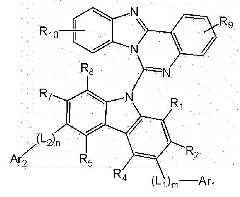
본 명세서는 상기 화학식 1로 표시되는 화합물를 제공한다.
본 출원의 일 실시상태에 따르면, 상기 화학식 1의 화합물은 이미다조퀴나졸린기와 카바졸기가 직접연결된 코어 구조를 가짐으로써 컨쥬게이션(conjugation)을 제한하는 역할을 한다. 화합물의 컨쥬게이션 길이와 에너지 밴드갭은 밀접한 관계가 있다. 구체적으로, 화합물의 컨쥬게이션 길이가 길수록 에너지 밴드갭이 작아진다. 전술한 바와 같이, 상기 화학식 1의 화합물의 코어는 제한된 컨쥬게이션을 포함하고 있으므로, 에너지 밴드 갭이 큰 성질을 갖는다. 통상 에너지 밴드 갭이 큰 코어 구조에 치환기를 도입하여 에너지 밴드 갭을 조절하는 것은 용이하나, 코어 구조가 에너지 밴드 갭이 작은 경우에는 치환기를 도입하여 에너지 밴드 갭을 크게 조절하기 어렵다. 이러한 관점에서, 상기 화학식 1의 화합물은 밴드 갭이 큰 구조를 가지므로, 밴드 갭의 조절이 용이하며, 예컨대 화학식 1의 R1 내지 R8 위치에 다양한 치환기를 도입함으로써 다양한 에너지 밴드 갭을 갖는 화합물을 합성할 수 있다. 따라서, 상기 화학식 1의 R1 내지 R8 및 다양한 치환기를 도입함으로써 화합물의 HOMO 및 LUMO 에너지 준위도 조절할 수 있다.
예컨대, 유기발광소자 제조시 사용되는 정공주입층 물질, 정공수송층 물질, 발광층 물질, 전자 수송층 물질에 주로 사용되는 치환기를 상기 코어구조에 도입함으로써 각 유기물층에서 요구하는 조건들을 충족시키는 물질을 합성할 수 있다. 예컨대, 상기 화학식 1이 코어 구조에 아릴 아민 구조를 포함하고 있으면, 유기 발광 소자에서 정공주입 및/또는 정공수송 물질로서의 적절한 에너지 준위를 가질 수 있다. 따라서, 본 출원에서는 상기 화학식 1의 화합물 중 치환기에 따라 적절한 에너지 준위를 갖는 화합물을 선택하여 유기 발광 소자에 사용함으로써 구동 전압이 낮고 광효율이 높은 소자를 구현할 수 있다.
또한, 상기 코어구조에 다양한 치환기를 대칭 또는 비대칭으로 도입함으로써 에너지 밴드 갭을 미세하게 조절이 가능하게 하며, 한편으로 유기물 사이에서의 계면에서의 특성을 향상되게 하며 물질의 용도를 다양하게 할 수 있다.
또한, 상기 화학식 1의 화합물은 안정한 산화 환원 특성을 나타낸다. 산화 환원에 대한 안정성은 CV(cyclovoltammetry) 방법을 이용하여 확인할 수 있다. 구체적인 예로서, 상기 화학식 1의 화합물은 여러 번의 반복 산화 전압을 가하였을 때 동일한 전압에서 산화가 일어나고 같은 전류 양을 보이는 것으로 나타났으며, 이것은 상기 화합물이 산화에 대한 안정성이 우수함을 나타낸다.
한편, 상기 화학식 1의 화합물은 유리 전이 온도(Tg)가 높아 열적 안정성이 우수하다. 예컨대, 화학식 1의 화합물은 유리 전이온도가 131℃로서, 기존에 일반적으로 사용되던 NPB(Tg: 96℃)에 비해 현저히 높음을 알 수 있다. 이러한 열적 안정성의 증가는 소자에 구동 안정성을 제공하는 중요한 요인이 된다.
또한, 상기 화학식 1의 화합물은 소자의 제조 공정 중 이용되는 용매, 예를 들어 자일렌, 디클로로 에탄, 혹은 NMP등과 같은 극성 용매등에 대한 용해도가 매우 우수하고, 용액을 이용한 방법을 통한 박막 형성에 용이한 특성을 가진다. 이에 따라, 제조 시 진공 증착법 뿐만 아니라 용액 도포법을 사용할 수 있다. 여기서, 용액 도포법이라 함은 스핀코팅, 딥코팅, 잉크젯프린팅, 스크린 프린팅, 스프레이법, 롤 코팅 등을 의미하지만, 이들만으로 한정되는 것은 아니다. 통상 용액 도포법에 의해 형성된 박막이나 고체 상태에서의 발광파장은 분자간 상호 작용에 의해 용액 상태의 발광 파장에 비해 장파장으로 이동하는 것을 흔히 볼 수 있는데, 상기 화학식 1의 화합물과 같은 구조를 갖는 화합물에서는 상기와 같은 파장의 이동이 거의 나타나지 않는 장점이 있다.
본 명세서에서 치환기의 예시들은 아래에서 설명하나, 이에 한정되는 것은 아니다.
상기 "치환"이라는 용어는 화합물의 탄소 원자에 결합된 수소 원자가 다른 치환기로 바뀌는 것을 의미하며, 치환되는 위치는 수소 원자가 치환되는 위치 즉, 치환기가 치환 가능한 위치라면 한정하지 않으며, 2 이상 치환되는 경우, 2 이상의 치환기는 서로 동일하거나 상이할 수 있다.
본 명세서에서 "치환 또는 비치환된" 이라는 용어는 중수소; 할로겐기; 시아노기; 니트로기; 히드록시기; 게르마늄기; 알킬기; 시클로알킬기; 알케닐기; 아민기; 실릴기; 포스포릴기; 아릴기; 및 헤테로고리기로 이루어진 군에서 선택된 1 또는 2 이상의 치환기로 치환되었거나 상기 예시된 치환기 중 2 이상의 치환기가 연결된 치환기로 치환되거나, 또는 어떠한 치환기도 갖지 않는 것을 의미한다. 예컨대, "2 이상의 치환기가 연결된 치환기"는 비페닐기일 수 있다. 즉, 비페닐기는 아릴기일 수도 있고, 2개의 페닐기가 연결된 치환기로 해석될 수 있다.
본 명세서에 있어서, 할로겐기의 예로는 불소, 염소, 브롬 또는 요오드가 있다.
본 명세서에 있어서, 에스테르기의 탄소수는 특별히 한정되지 않으나, 탄소수 1 내지 50인 것이 바람직하다. 구체적으로, 하기 구조식의 화합물이 될 수 있으나, 이에 한정되는 것은 아니다.
Figure PCTKR2016006014-appb-I000002
본 명세서에서 카보닐기의 탄소수는 특별히 한정되지 않으나, 탄소수 1 내지 50인 것이 바람직하다. 구체적으로 하기와 같은 구조의 화합물이 될 수 있으나, 이에 한정되는 것은 아니다.
Figure PCTKR2016006014-appb-I000003
본 명세서에 있어서, 상기 알킬기는 직쇄 또는 분지쇄일 수 있고, 탄소수는 특별히 한정되지 않으나 1 내지 50인 것이 바람직하다. 구체적인 예로는 메틸기, 에틸기, 프로필기, n-프로필기, 이소프로필기, 부틸기, n-부틸기, 이소부틸기, tert-부틸기, sec-부틸기, 1-메틸-부틸기, 1-에틸-부틸기, 펜틸기, n-펜틸기, 이소펜틸기, 네오펜틸기, tert-펜틸기, 헥실기, n-헥실기, 1-메틸펜틸기, 2-메틸펜틸기, 4-메틸-2-펜틸기, 3,3-디메틸부틸기, 2-에틸부틸기, 헵틸기, n-헵틸기, 1-메틸헥실기, 시클로펜틸메틸기, 시클로헥실메틸기, 옥틸기, n-옥틸기, tert-옥틸기, 1-메틸헵틸기, 2-에틸헥실기, 2-프로필펜틸기, n-노닐기, 2,2-디메틸헵틸기, 1-에틸-프로필기, 1,1-디메틸-프로필기, 이소헥실기, 2-메틸펜틸기, 4-메틸헥실기, 5-메틸헥실기 등이 있으나, 이들에 한정되지 않는다.
본 명세서에 있어서, 시클로알킬기는 특별히 한정되지 않으나, 탄소수 3 내지 60인 것이 바람직하며, 구체적으로 시클로프로필기, 시클로부틸기, 시클로펜틸기, 3-메틸시클로펜틸기, 2,3-디메틸시클로펜틸기, 시클로헥실기, 3-메틸시클로헥실기, 4-메틸시클로헥실기, 2,3-디메틸시클로헥실기, 3,4,5-트리메틸시클로헥실기, 4-tert-부틸시클로헥실기, 시클로헵틸기, 시클로옥틸기 등이 있으나, 이에 한정되지 않는다.
본 명세서에 있어서, 상기 알콕시기는 직쇄, 분지쇄 또는 고리쇄일 수 있다. 알콕시기의 탄소수는 특별히 한정되지 않으나, 탄소수 1 내지 20인 것이 바람직하다. 구체적으로, 메톡시기, 에톡시기, n-프로폭시기, 이소프로폭시기, i-프로필옥시기, n-부톡시기, 이소부톡시기, tert-부톡시기, sec-부톡시기, n-펜틸옥시기, 네오펜틸옥시기, 이소펜틸옥시기, n-헥실옥시기, 3,3-디메틸부틸옥시기, 2-에틸부틸옥시기, n-옥틸옥시기, n-노닐옥시기, n-데실옥시기, 벤질옥시기, p-메틸벤질옥시기 등이 될 수 있으나, 이에 한정되는 것은 아니다.
본 명세서에 있어서, 상기 알케닐기는 직쇄 또는 분지쇄일 수 있고, 탄소수는 특별히 한정되지 않으나, 2 내지 40인 것이 바람직하다. 구체적인 예로는 비닐기, 1-프로페닐기, 이소프로페닐기, 1-부테닐기, 2-부테닐기, 3-부테닐기, 1-펜테닐기, 2-펜테닐기, 3-펜테닐기, 3-메틸-1-부테닐기, 1,3-부타디에닐기, 알릴기, 1-페닐비닐-1-일기, 2-페닐비닐-1-일기, 2,2-디페닐비닐-1-일기, 2-페닐-2-(나프틸-1-일)비닐-1-일기, 2,2-비스(디페닐-1-일)비닐-1-일기, 스틸베닐기, 스티레닐기 등이 있으나 이들에 한정되지 않는다.
본 명세서에서 상기 아릴기가 단환식 아릴기인 경우 탄소수는 특별히 한정되지 않으나, 탄소수 6 내지 25인 것이 바람직하다. 구체적으로 단환식 아릴기로는 페닐기, 비페닐기, 터페닐기 등이 될 수 있으나, 이에 한정되는 것은 아니다.
상기 아릴기가 다환식 아릴기인 경우 탄소수는 특별히 한정되지 않으나. 탄소수 10 내지 24인 것이 바람직하다. 구체적으로 다환식 아릴기로는 나프틸기, 안트라세닐기, 페난트릴기, 파이레닐기, 페릴레닐기, 크라이세닐기, 플루오레닐기 등이 될 수 있으나, 이에 한정되는 것은 아니다.
본 명세서에 있어서, 상기 플루오레닐기는 치환될 수 있으며, 인접한 치환기들이 서로 결합하여 고리를 형성할 수 있다.
상기 플루오레닐기가 치환되는 경우,
Figure PCTKR2016006014-appb-I000004
,
Figure PCTKR2016006014-appb-I000005
,
Figure PCTKR2016006014-appb-I000006
,
Figure PCTKR2016006014-appb-I000007
,
Figure PCTKR2016006014-appb-I000008
,
Figure PCTKR2016006014-appb-I000009
등이 될 수 있으나, 이에 한정되는 것은 아니다.
본 명세서에 있어서, 헤테로고리기는 탄소가 아닌 원자, 이종원자를 1 이상 포함하는 것으로서, 구체적으로 상기 이종 원자는 O, N, Se 및 S 등으로 이루어진 군에서 선택되는 원자를 1 이상 포함할 수 있다. 헤테로고리기의 탄소수는 특별히 한정되지 않으나, 탄소수 2 내지 60인 것이 바람직하다. 헤테로고리기의 예로는 티오페닐기, 퓨라닐기, 피롤기, 이미다졸릴기, 티아졸릴기, 옥사졸릴기, 옥사디아졸릴기, 트리아졸릴기, 피리딜기, 비피리딜기, 피리미딜기, 트리아지닐기, 아크리딜기, 피리다지닐기, 피라지닐기, 퀴놀리닐기, 퀴나졸리닐기, 퀴녹살리닐기, 프탈라지닐기, 피리도피리미디닐기, 피리도피라지닐기, 피라지노피라지닐기, 이소퀴놀리닐기, 인돌기, 카바졸릴기, 벤즈옥사졸릴기, 벤즈이미다졸릴기, 벤조티아졸릴기, 벤조카바졸릴기, 디벤조카바졸릴기, 벤조티오페닐기, 디벤조티오페닐기, 벤조퓨라닐기, 페난트롤리닐기(phenanthrolinyl group), 티아졸릴기, 이소옥사졸릴기, 옥사디아졸릴기, 티아디아졸릴기, 벤조티아졸릴기, 페노티아지닐기, 페노옥사지닐기, 디벤조퓨란기 및 이들의 축합구조 등이 있으나, 이들에만 한정되는 것은 아니다. 이외에도 헤테로고리기의 예로서, 술포닐기를 포함하는 헤테로고리 구조, 예컨대,
Figure PCTKR2016006014-appb-I000010
등이 있다.
본 명세서에 있어서, 상기 축합구조는 해당 치환기에 방향족 탄화수소 고리가 축합된 구조일 수 있다. 예컨대, 벤즈이미다졸의 축합고리로서
Figure PCTKR2016006014-appb-I000011
,
Figure PCTKR2016006014-appb-I000012
,
Figure PCTKR2016006014-appb-I000013
등이 될 수 있으나, 이에 한정되는 것은 아니다.
본 명세서에 있어서, "인접한" 기는 해당 치환기가 치환된 원자와 직접 연결된 원자에 치환된 치환기, 해당 치환기와 입체구조적으로 가장 가깝게 위치한 치환기, 또는 해당 치환기가 치환된 원자에 치환된 다른 치환기를 의미할 수 있다. 예컨대, 벤젠고리에서 오쏘(ortho)위치로 치환된 2개의 치환기 및 지방족 고리에서 동일 탄소에 치환된 2개의 치환기는 서로 "인접한" 기로 해석될 수 있다.
본 명세서에 있어서, 인접한 기가 서로 결합하여 고리를 형성하는 것의 의미는 전술한 바와 같이 인접한 기가 서로 결합하여, 5원 내지 8원의 탄화수소 고리 또는 5원 내지 8원의 헤테로고리를 형성하는 것을 의미하며, 단환 또는 다환일 수 있으며, 지방족, 방향족 또는 이들의 축합된 형태일 수 있으며 이를 한정하지 않는다.
본 명세서에서 탄화수소고리 또는 헤테로고리는 1 가기인 것을 제외하고, 전술한 시클로알킬기, 아릴기 또는 헤테로고리기의 예시 중에서 선택될 수 있으며, 단환 또는 다환, 지방족 또는 방향족 또는 이들의 축합된 형태일 수 있으나. 이들에만 한정되는 것은 아니다.
본 명세서에서 아민기는 아미노기(-NH2)의 적어도 하나의 수소 원자가 다른 치환체로 치환된 1가의 아민을 의미한다. 예컨대, 상기 아민기는 -NR100R101로 표시되고, R100 및 R101은 서로 동일하거나 상이하며, 각각 독립적으로 수소; 중수소; 할로겐기; 알킬기; 알케닐기; 알콕시기; 시클로알킬기; 아릴기; 및 헤테로고리기 중 적어도 하나로 이루어진 치환기일 수 있다(단, R100 및 R101 중 적어도 하나는 수소가 아니다). 예컨대, 상기 아민기가 치환체로 알킬기 및 아릴기를 가지는 경우의 구체적인 예로는 디페닐아민기, 비페닐비페닐아민기, 페닐비페닐아민기, 페닐터페닐아민기, 페닐플루오레닐아민, 페닐(디메틸플루오레닐)아민기, 비페닐(디메틸플루오레닐)아민기 등이 있으나, 이에만 한정되는 것은 아니다.
본 명세서에서 포스포릴기는 P(=O)를 포함하고 상기 P 원자가 라디칼로서 직접 연결되는 치환기이며, -P(=O)R102R103로 표시되고, R102 및 R103은 서로 동일하거나 상이하며, 각각 독립적으로 수소; 중수소; 할로겐기; 알킬기; 알케닐기; 알콕시기; 시클로알킬기; 아릴기; 및 헤테로고리기 중 적어도 하나로 이루어진 치환기일 수 있다. 예컨대, 상기 포스포릴기가 치환체로 아릴기를 가지는 경우의 구체적인 예로는 디페닐포스포릴기, 페닐비페닐포스포릴기, 비페닐비페닐포스포릴기, 페닐터페닐포스포릴기, 비페닐터페닐포스포릴기 등이 있으나, 이에만 한정되는 것은 아니다.
본 명세서에서 실릴기는 Si를 포함하고 상기 Si 원자가 라디칼로서 직접 연결되는 치환기이며, -SiR104R105R106로 표시되고, R104 내지 R106은 서로 동일하거나 상이하며, 각각 독립적으로 수소; 중수소; 할로겐기; 알킬기; 알케닐기; 알콕시기; 시클로알킬기; 아릴기; 및 헤테로고리기 중 적어도 하나로 이루어진 치환기일 수 있다. 예컨대, 상기 실릴기가 치환체로 알킬기를 가지는 경우의 구체적인 예로는 트리메틸실릴기가 있으나, 이에만 한정되는 것은 아니다. 또한, 상기 실릴기가 치환체로 아릴기를 가지는 경우의 구체적인 예로는 트리페닐실릴기가 있으나, 이에만 한정되는 것은 아니다.
본 명세서에 있어서, 게르마늄기는 -GeRaRbRc의 화학식으로 표시될 수 있고, 상기 Ra, Rb 및 Rc는 각각 수소; 치환 또는 비치환된 알킬기; 또는 치환 또는 비치환된 아릴기일 수 있다. 상기 게르마늄기는 구체적으로 트리메틸게르마늄기, 트리에틸게르마늄기, t-부틸디메틸게르마늄기 등이 있으나, 이에 한정되지 않는다.
본 명세서에서 아릴옥시기, 아릴싸이오기 중의 아릴기는 전술한 아릴기에 관한 설명이 적용될 수 있다.
본 명세서에서 아르알킬기 중 알킬기는 전술한 알킬기에 관한 설명이 적용될 수 있다.
본 명세서에서 헤테로아릴기는 방향족인 것을 제외하고는 전술한 헤테로고리기에 관한 설명이 적용될 수 있다.
본 명세서에서 알콕시카보닐기 중 알콕시기는 전술한 알킬기에 관한 설명이 적용되고, 알콕시카보닐기 중 카보닐기는 전술한 카보닐기에 관한 설명이 적용될 수 있다.
본 출원의 일 실시상태에 따르면, R1 내지 R4 중 인접한 하나의 쌍은 서로 결합하여 고리를 형성한다.
본 출원의 일 실시상태에 따르면, R1 내지 R4 중 인접한 하나의 쌍은 서로 결합하여 방향족 탄화수소 고리를 형성한다.
본 출원의 일 실시상태에 따르면, R1 내지 R4 중 인접한 하나의 쌍은 서로 결합하여 방향족 6원고리를 형성한다.
본 출원의 일 실시상태에 따르면, R5 내지 R8 중 인접한 하나의 쌍은 서로 결합하여 고리를 형성한다.
본 출원의 일 실시상태에 따르면, R5 내지 R8 중 인접한 하나의 쌍은 서로 결합하여 방향족 탄화수소 고리를 형성한다.
본 출원의 일 실시상태에 따르면, R5 내지 R8 중 인접한 하나의 쌍은 서로 결합하여 방향족 6원고리를 형성한다.
본 출원의 일 실시상태에 따르면, 상기 화학식 1은 하기 화학식 2 또는 3으로 표시된다.
[화학식 2]
Figure PCTKR2016006014-appb-I000014
[화학식 3]
Figure PCTKR2016006014-appb-I000015
상기 화학식 2 및 3에 있어서,
R1 내지 R10은 화학식 1에서 정의한 바와 동일하고,
R11 및 R12는 서로 동일하거나 상이하며, 각각 독립적으로 수소; 중수소; 할로겐기; 니트로기; 시아노기; 에스테르기; 카보닐기; 치환 또는 비치환된 알킬기; 치환 또는 비치환된 시클로알킬기; 치환 또는 비치환된 알콕시기; 치환 또는 비치환된 알케닐기; 치환 또는 비치환된 아릴기; 또는 치환 또는 비치환된 헤테로고리기이고,
p 및 q는 각각 0 내지 4의 정수이다.
본 출원의 일 실시상태에 따르면, 상기 R3는 -(L)m-(Ar)n이다.
본 출원의 일 실시상태에 따르면, 상기 R2는 -(L)m-(Ar)n이다.
본 출원의 일 실시상태에 따르면, 상기 R3 및 R6는 -(L)m-(Ar)n이고, 상기 R3 및 R6는 서로 동일하거나 상이하다.
본 출원의 일 실시상태에 따르면, 상기 R2 및 R7은 -(L)m-(Ar)n이고, 상기 R2 및 R7은 서로 동일하거나 상이하다.
본 출원의 일 실시상태에 따르면, 상기 화학식 1은 하기 화학식 4 내지 7 중 어느 하나로 표시된다.
[화학식 4]
Figure PCTKR2016006014-appb-I000016
[화학식 5]
Figure PCTKR2016006014-appb-I000017
[화학식 6]
Figure PCTKR2016006014-appb-I000018
[화학식 7]
Figure PCTKR2016006014-appb-I000019
상기 화학식 4 내지 7에 있어서, L, L1 및 L2는 상기 화학식 1의 L의 정의와 동일하고, Ar, Ar1 및 Ar2는 상기 화학식 1의 Ar의 정의와 동일하며, m 및 n은 화학식 1의 m의 정의와 동일하며, R1 내지 R10은 화학식 1에서 정의한 바와 동일하다.
본 출원의 일 실시상태에 따르면, 상기 L은 직접결합 또는 치환 또는 비치환된 아릴렌기이다.
본 출원의 일 실시상태에 따르면, 상기 L은 직접결합; 치환 또는 비치환된 페닐렌기; 치환 또는 비치환된 비페닐렌기; 치환 또는 비치환된 나프틸렌기; 치환 또는 비치환된 안트라세닐렌기; 치환 또는 비치환된 플루오레닐렌기; 치환 또는 비치환된 페난트레닐렌기; 치환 또는 비치환된 파이레닐렌기; 및 치환 또는 비치환된 크라이세닐렌기로 이루어진 군에서 선택된다.
본 출원의 일 실시상태에 따르면, 상기 L은 직접결합; 페닐렌기; 비페닐렌기; 나프틸렌기; 안트라세닐렌기; 플루오레닐렌기; 페난트레닐렌기; 파이레닐렌기; 및 크라이세닐렌기로 이루어진 군에서 선택된다.
본 출원의 일 실시상태에 따르면, 상기 L은 직접결합; 또는 치환 또는 비치환된 페닐렌기이다.
본 출원의 일 실시상태에 따르면, 상기 L은 직접결합; 또는 페닐렌기이다.
본 출원의 일 실시상태에 따르면 m은 1이다.
본 출원의 일 실시상태에 따르면 m은 2이고, 2개의 L은 서로 동일하거나 상이하다.
본 출원의 일 실시상태에 따르면 m은 3이고, 3개의 L은 서로 동일하거나 상이하다.
본 출원의 일 실시상태에 따르면, 상기 L1 및 L2는 전술한 L의 정의와 동일하다.
본 출원의 일 실시상태에 따르면, 상기 Ar은 치환된 단환의 아릴기; 치환 또는 비치환된 다환의 아릴기; 치환 또는 비치환된 헤테로고리기; 치환 또는 비치환된 아민기; 치환 또는 비치환된 실릴기; 또는 치환 또는 비치환된 포스포릴기이다.
본 출원의 일 실시상태에 따르면, 상기 Ar은 치환된 단환의 아릴기; 치환 또는 비치환된 다환의 아릴기; 치환 또는 비치환된 헤테로고리기; 치환 또는 비치환된 아민기; 치환 또는 비치환된 실릴기; 또는 치환 또는 비치환된 포스포릴기이고, 상기 치환 또는 비치환된은 중수소; 할로겐기; 시아노기; C1 내지 C60의 알킬기; C6 내지 C60의 시클로알킬기; C6 내지 C60의 아릴기; 및 C2 내지 C60의 헤테로고리기로 이루어진 군으로부터 선택되는 적어도 하나로 치환 또는 비치환된 것을 의미한다.
본 출원의 일 실시상태에 따르면, 상기 Ar은 치환된 단환의 아릴기; 치환 또는 비치환된 다환의 아릴기; 치환 또는 비치환된 헤테로고리기; 치환 또는 비치환된 아민기; 치환 또는 비치환된 실릴기; 또는 치환 또는 비치환된 포스포릴기이고, 상기 치환 또는 비치환된은 중수소; 할로겐기; C1 내지 C20의 알킬기; 시아노기; C6 내지 C20의 아릴기; 및 C2 내지 C20의 헤테로고리기로 이루어진 군으로부터 선택되는 적어도 하나로 치환 또는 비치환된 것을 의미한다.
본 출원의 일 실시상태에 따르면, 상기 치환된 단환의 아릴기는 중수소; 할로겐기; C1 내지 C20의 알킬기; 시아노기; C6 내지 C20의 아릴기; 및 C2 내지 C20의 헤테로고리기로 이루어진 군으로부터 선택되는 적어도 하나로 치환된 페닐기이다.
본 출원의 일 실시상태에 따르면, 상기 치환된 단환의 아릴기는 중수소; 할로겐기; 메틸기; t-부틸기; 시아노기; 페닐기; 비페닐기; 나프틸기; 안트라세닐기; 페난트레닐기; 피리딜기; 피리미딜기; 및 트리아지닐기로 이루어진 군으로부터 선택되는 적어도 하나로 치환된 페닐기이다.
본 출원의 일 실시상태에 따르면, 상기 다환의 아릴기는 치환 또는 비치환된 나프틸기; 치환 또는 비치환된 안트라세닐기; 치환 또는 비치환된 페난트레닐기; 치환 또는 비치환된 크라이세닐기; 치환 또는 비치환된 파이레닐기; 치환 또는 비치환된 트리페닐레닐기; 또는 치환 또는 비치환된 플루오레닐기이다.
본 출원의 일 실시상태에 따르면, 상기 다환의 아릴기는 치환 또는 비치환된 나프틸기; 치환 또는 비치환된 안트라세닐기; 치환 또는 비치환된 페난트레닐기; 치환 또는 비치환된 크라이세닐기; 치환 또는 비치환된 파이레닐기; 치환 또는 비치환된 트리페닐레닐기; 또는 치환 또는 비치환된 플루오레닐기이고, 상기 치환 또는 비치환된은 중수소; 할로겐기; C1 내지 C20의 알킬기; 시아노기; C6 내지 C20의 아릴기; 및 C2 내지 C20의 헤테로고리기로 이루어진 군으로부터 선택되는 적어도 하나로 치환 또는 비치환된 것을 의미한다.
본 출원의 일 실시상태에 따르면, 상기 다환의 아릴기는 치환 또는 비치환된 나프틸기; 치환 또는 비치환된 안트라세닐기; 치환 또는 비치환된 페난트레닐기; 치환 또는 비치환된 크라이세닐기; 치환 또는 비치환된 파이레닐기; 치환 또는 비치환된 트리페닐레닐기; 또는 치환 또는 비치환된 플루오레닐기이고, 상기 치환 또는 비치환된은 중수소; 할로겐기; 메틸기; t-부틸기; 시아노기; 페닐기; 비페닐기; 나프틸기; 안트라세닐기; 페난트레닐기; 피리딜기; 피리미딜기; 및 트리아지닐기로 이루어진 군으로부터 선택되는 적어도 하나로 치환 또는 비치환된 것을 의미한다.
본 출원의 일 실시상태에 따르면, 상기 헤테로고리기는 치환 또는 비치환된 피리딜기; 치환 또는 비치환된 피리미딜기; 치환 또는 비치환된 트리아지닐기; 치환 또는 비치환된 티오페닐기; 치환 또는 비치환된 퓨라닐기; 치환 또는 비치환된 벤조퓨라닐기; 치환 또는 비치환된 벤조티오페닐기; 치환 또는 비치환된 디벤조퓨라닐기; 치환 또는 비치환된 디벤조티오페닐기; 치환 또는 비치환된 카바졸릴기; 치환 또는 비치환된 벤조카바졸릴기; 치환 또는 비치환된 디벤조카바졸릴기; 치환 또는 비치환된 이미다졸릴기; 치환 또는 비치환된 벤즈이미다졸릴기; 치환 또는 비치환된 디벤즈이미다졸릴기; 치환 또는 비치환된 티아졸릴기; 치환 또는 비치환된 벤조티아졸릴기; 치환 또는 비치환된 옥사졸릴기; 치환 또는 비치환된 벤즈옥사졸릴기; 치환 또는 비치환된 페난트롤리닐기; 치환 또는 비치환된 페노티아지닐기; 치환 또는 비치환된 페노옥사지닐기; 치환 또는 비치환된 퀴놀리닐기; 치환 또는 비치환된 1가의
Figure PCTKR2016006014-appb-I000020
기; 치환 또는 비치환된 1가의
Figure PCTKR2016006014-appb-I000021
기; 치환 또는 비치환된 1가의
Figure PCTKR2016006014-appb-I000022
기; 또는 치환 또는 비치환된 1가의
Figure PCTKR2016006014-appb-I000023
기 이고, 상기 치환 또는 비치환된은 중수소; 할로겐기; C1 내지 C20의 알킬기; 시아노기; C6 내지 C20의 아릴기; 및 C2 내지 C20의 헤테로고리기로 이루어진 군으로부터 선택되는 적어도 하나로 치환 또는 비치환된 것을 의미한다.
본 출원의 일 실시상태에 따르면, 상기 헤테로고리기는 치환 또는 비치환된 피리딜기; 치환 또는 비치환된 피리미딜기; 치환 또는 비치환된 트리아지닐기; 치환 또는 비치환된 티오페닐기; 치환 또는 비치환된 퓨라닐기; 치환 또는 비치환된 벤조퓨라닐기; 치환 또는 비치환된 벤조티오페닐기; 치환 또는 비치환된 디벤조퓨라닐기; 치환 또는 비치환된 디벤조티오페닐기; 치환 또는 비치환된 카바졸릴기; 치환 또는 비치환된 벤조카바졸릴기; 치환 또는 비치환된 디벤조카바졸릴기; 치환 또는 비치환된 이미다졸릴기; 치환 또는 비치환된 벤즈이미다졸릴기; 치환 또는 비치환된 디벤즈이미다졸릴기; 치환 또는 비치환된 티아졸릴기; 치환 또는 비치환된 벤조티아졸릴기; 치환 또는 비치환된 옥사졸릴기; 치환 또는 비치환된 벤즈옥사졸릴기; 치환 또는 비치환된 페난트롤리닐기; 치환 또는 비치환된 페노티아지닐기; 치환 또는 비치환된 페노옥사지닐기; 치환 또는 비치환된 퀴놀리닐기; 치환 또는 비치환된 1가의
Figure PCTKR2016006014-appb-I000024
기; 치환 또는 비치환된 1가의
Figure PCTKR2016006014-appb-I000025
기; 치환 또는 비치환된 1가의
Figure PCTKR2016006014-appb-I000026
기; 또는 치환 또는 비치환된 1가의
Figure PCTKR2016006014-appb-I000027
기 이고, 상기 치환 또는 비치환된은 중수소; 할로겐기; 메틸기; t-부틸기; 시아노기; 페닐기; 비페닐기; 나프틸기; 안트라세닐기; 페난트레닐기; 피리딜기; 피리미딜기; 및 트리아지닐기로 이루어진 군으로부터 선택되는 적어도 하나로 치환 또는 비치환된 것을 의미한다.
본 출원의 일 실시상태에 따르면, 상기 Ar1 및 Ar2는 전술한 Ar의 정의와 동일하다.
본 출원의 일 실시상태에 따르면, 상기 아민기는 -NR100R101로 표시되고, 상기 R100 및 R101은 서로 동일하거나 상이하며, 각각 독립적으로 치환 또는 비치환된 C1 내지 C60의 알킬기; 치환 또는 비치환된 C6 내지 C60의 시클로알킬기; 치환 또는 비치환된 C6 내지 C60의 아릴기; 또는 치환 또는 비치환된 C2 내지 C60의 헤테로고리기일 수 있다.
본 출원의 일 실시상태에 따르면, 상기 R100 및 R101은 치환 또는 비치환된 C6 내지 C60의 아릴기이고, R100 및 R101은 서로 동일하거나 상이할 수 있다.
본 출원의 일 실시상태에 따르면, 상기 상기 R100 및 R101은 C1 내지 C60의 알킬기로 치환 또는 비치환된 C6 내지 C60의 아릴기이고, 상기 R100 및 R101은 서로 동일하거나 상이할 수 있다.
본 출원의 일 실시상태에 따르면, 상기 상기 R100 및 R101은 서로 동일하거나 상이하고, 각각 독립적으로 페닐기, 비페닐기, 나프틸기, 터페닐기, 플루오렌기 또는 디메틸 플루오렌기일 수 있다.
본 출원의 일 실시상태에 따르면, 상기 포스포릴기는 -P(=O)R102R103로 표시되고, 상기 R102 및 R103은 서로 동일하거나 상이하며, 각각 독립적으로 치환 또는 비치환된 C1 내지 C60의 알킬기; 치환 또는 비치환된 C6 내지 C60의 시클로알킬기; 치환 또는 비치환된 C6 내지 C60의 아릴기; 또는 치환 또는 비치환된 C2 내지 C60의 헤테로고리기일 수 있다.
본 출원의 일 실시상태에 따르면, 상기 R102 및 R103은 치환 또는 비치환된 C6 내지 C60의 아릴기이고, R102 및 R103은 서로 동일하거나 상이할 수 있다.
본 출원의 일 실시상태에 따르면, 상기 상기 R102 및 R103은 서로 동일하거나 상이하고, 각각 독립적으로 페닐기, 비페닐기, 나프틸기, 터페닐기, 플루오렌기 또는 디메틸 플루오렌기일 수 있다.
본 출원의 일 실시상태에 따르면, 상기 실릴기는 -SiR104R105R106으로 표시되고, 상기 R104 내지 R106은 서로 동일하거나 상이하며, 각각 독립적으로 치환 또는 비치환된 C1 내지 C60의 알킬기; 치환 또는 비치환된 C6 내지 C60의 시클로알킬기; 치환 또는 비치환된 C6 내지 C60의 아릴기; 또는 치환 또는 비치환된 C2 내지 C60의 헤테로고리기일 수 있다.
본 출원의 일 실시상태에 따르면, 상기 R104 내지 R106은 서로 동일하거나 상이하고, 각각 독립적으로 치환 또는 비치환된 C1 내지 C60의 알킬기; 또는 치환 또는 비치환된 C6 내지 C60의 아릴기이다.
본 출원의 일 실시상태에 따르면, 상기 상기 R104 내지 R106은 서로 동일하거나 상이하고, 각각 독립적으로 메틸기, 에틸기, 페닐기, 비페닐기, 나프틸기, 터페닐기, 플루오렌기 또는 디메틸 플루오렌기일 수 있다.
본 출원의 일 실시상태에 따르면, 상기 -(L)m-(Ar)n은 하기 그룹 1 내지 4의 구조식들 중에서 선택되는 어느 하나일 수 있다.
[그룹 1]
Figure PCTKR2016006014-appb-I000028
Figure PCTKR2016006014-appb-I000029
Figure PCTKR2016006014-appb-I000030
Figure PCTKR2016006014-appb-I000031
[그룹 2]
Figure PCTKR2016006014-appb-I000032
Figure PCTKR2016006014-appb-I000033
Figure PCTKR2016006014-appb-I000034
Figure PCTKR2016006014-appb-I000035
[그룹 3]
Figure PCTKR2016006014-appb-I000036
[그룹 4]
Figure PCTKR2016006014-appb-I000037
상기 그룹 1, 2 및 4에서 "
Figure PCTKR2016006014-appb-I000038
"는 결합하는 위치를 의미한다.
상기 그룹 2에서 플루오렌기에 치환된 메틸기를 제외한 "
Figure PCTKR2016006014-appb-I000039
"는 결합하는 위치를 의미한다.
상기 그룹 3에서 플루오렌기에 치환된 메틸기를 제외한 "
Figure PCTKR2016006014-appb-I000040
"는 결합하는 위치를 의미한다. 즉, N에 연결된 "
Figure PCTKR2016006014-appb-I000041
"는 결합하는 위치를 의미한다.
본 출원의 일 실시상태에 따르면 n은 1이다.
본 출원의 일 실시상태에 따르면 n은 2이고, 2개의 Ar은 서로 동일하거나 상이하다.
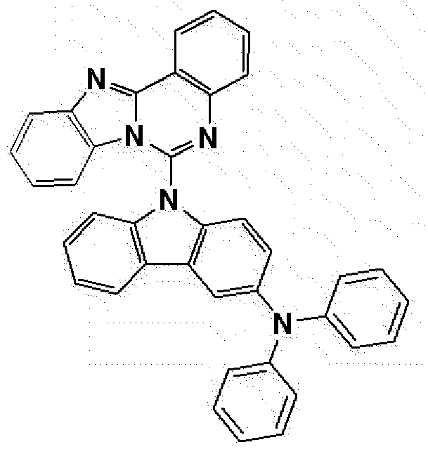
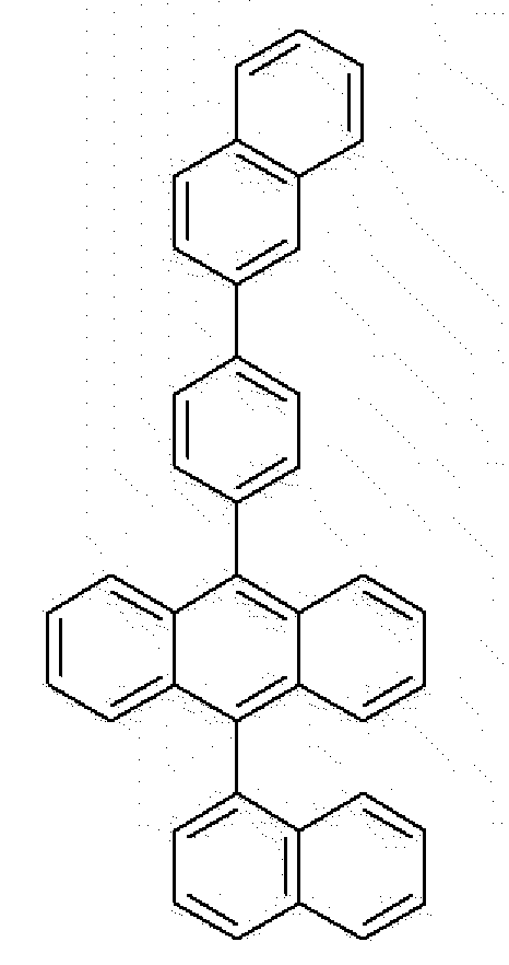
본 출원의 일 실시상태에 따르면, 상기 화학식 1로 표시되는 화합물은 하기 구조식들 중에서 선택되는 어느 하나일 수 있다.
Figure PCTKR2016006014-appb-I000042
Figure PCTKR2016006014-appb-I000043
Figure PCTKR2016006014-appb-I000044
Figure PCTKR2016006014-appb-I000045
Figure PCTKR2016006014-appb-I000046
Figure PCTKR2016006014-appb-I000047
Figure PCTKR2016006014-appb-I000048
Figure PCTKR2016006014-appb-I000049
Figure PCTKR2016006014-appb-I000050
Figure PCTKR2016006014-appb-I000051
Figure PCTKR2016006014-appb-I000052
Figure PCTKR2016006014-appb-I000053
Figure PCTKR2016006014-appb-I000054
Figure PCTKR2016006014-appb-I000055
Figure PCTKR2016006014-appb-I000056
Figure PCTKR2016006014-appb-I000057
Figure PCTKR2016006014-appb-I000058
Figure PCTKR2016006014-appb-I000059
Figure PCTKR2016006014-appb-I000060
Figure PCTKR2016006014-appb-I000061
Figure PCTKR2016006014-appb-I000062
Figure PCTKR2016006014-appb-I000063
Figure PCTKR2016006014-appb-I000064
Figure PCTKR2016006014-appb-I000065
Figure PCTKR2016006014-appb-I000066
Figure PCTKR2016006014-appb-I000067
Figure PCTKR2016006014-appb-I000068
Figure PCTKR2016006014-appb-I000069
Figure PCTKR2016006014-appb-I000070
Figure PCTKR2016006014-appb-I000071
Figure PCTKR2016006014-appb-I000072
Figure PCTKR2016006014-appb-I000073
Figure PCTKR2016006014-appb-I000074
Figure PCTKR2016006014-appb-I000075
Figure PCTKR2016006014-appb-I000076
Figure PCTKR2016006014-appb-I000077
Figure PCTKR2016006014-appb-I000078
Figure PCTKR2016006014-appb-I000079
Figure PCTKR2016006014-appb-I000080
Figure PCTKR2016006014-appb-I000081
Figure PCTKR2016006014-appb-I000082
Figure PCTKR2016006014-appb-I000083
Figure PCTKR2016006014-appb-I000084
Figure PCTKR2016006014-appb-I000085
Figure PCTKR2016006014-appb-I000086
Figure PCTKR2016006014-appb-I000087
Figure PCTKR2016006014-appb-I000088
Figure PCTKR2016006014-appb-I000089
Figure PCTKR2016006014-appb-I000090
Figure PCTKR2016006014-appb-I000091
Figure PCTKR2016006014-appb-I000092
Figure PCTKR2016006014-appb-I000093
Figure PCTKR2016006014-appb-I000094
Figure PCTKR2016006014-appb-I000095
Figure PCTKR2016006014-appb-I000096
Figure PCTKR2016006014-appb-I000097
Figure PCTKR2016006014-appb-I000098
Figure PCTKR2016006014-appb-I000099
Figure PCTKR2016006014-appb-I000100
Figure PCTKR2016006014-appb-I000101
Figure PCTKR2016006014-appb-I000102
Figure PCTKR2016006014-appb-I000103
Figure PCTKR2016006014-appb-I000104
Figure PCTKR2016006014-appb-I000105
Figure PCTKR2016006014-appb-I000106
Figure PCTKR2016006014-appb-I000107
Figure PCTKR2016006014-appb-I000108
Figure PCTKR2016006014-appb-I000109
Figure PCTKR2016006014-appb-I000110
Figure PCTKR2016006014-appb-I000111
Figure PCTKR2016006014-appb-I000112
Figure PCTKR2016006014-appb-I000113
Figure PCTKR2016006014-appb-I000114
Figure PCTKR2016006014-appb-I000115
Figure PCTKR2016006014-appb-I000116
Figure PCTKR2016006014-appb-I000117
Figure PCTKR2016006014-appb-I000118
Figure PCTKR2016006014-appb-I000119
본 출원의 일 실시상태에 따른 화합물은 후술하는 제조 방법으로 제조될 수 있다.
예컨대, 상기 화학식 1의 화합물은 하기 일반식 1 내지 6과 같이 코어 구조가 제조될 수 있다. 치환기는 당기술분야에 알려져 있는 방법에 의하여 결합될 수 있으며, 치환기의 종류, 위치 또는 개수는 당기술분야에 알려져 있는 기술에 따라 변경될 수 있다.
[일반식 1]
Figure PCTKR2016006014-appb-I000120
[일반식 2]
Figure PCTKR2016006014-appb-I000121
[일반식 3]
Figure PCTKR2016006014-appb-I000122
[일반식 4]
Figure PCTKR2016006014-appb-I000123
[일반식 5]
Figure PCTKR2016006014-appb-I000124
[일반식 6]
Figure PCTKR2016006014-appb-I000125
상기 일반식 1 내지 6에서 제조된 코어에서 Br의 위치가 상기 -(L)m-Ar로 치환되는 위치일 수 있다.
전술한 바와 같이, 치환기는 당기술분야에 알려져 있는 방법에 의하여 결합될 수 있으며, 치환기의 종류, 위치 또는 개수는 당기술분야에 알려져 있는 기술에 따라 변경될 수 있다. 예컨대, 하기 일반식 7 내지 9에 의하여 아민기, 아릴기, 헤테로고리기 등의 치환기를 연결할 수 있다.
[일반식 7]
Figure PCTKR2016006014-appb-I000126
[일반식 8]
Figure PCTKR2016006014-appb-I000127
[일반식 9]
Figure PCTKR2016006014-appb-I000128
상기 일반식 7은 부끄발드 아미네이션(Buchwald amination)을 이용하여 아민, 아릴아민 등의 치환체를 연결하는 반응식을 나타낸 것이다. 여기서, 상기 Ar은 수소 또는 추가의 치환기를 의미한다.
상기 일반식 8 및 9는 보릴레이션 방법 및 스즈키커플링(Suzuki coupling)을 이용하여 아릴기, 헤테로고리기 등의 치환체를 연결하는 반응식을 나타낸 것이다. 특히, 상기 일반식 9는 단환의 아릴기 또는 단환의 N함유 헤테로고리기의 치환체를 연결하는 반응식을 나타낸 것이다. 상기 X1 내지 X3는 탄소 또는 질소이며, 상기 Ar은 수소 또는 추가의 치환기를 의미한다.
상기 일반식 1 내지 9는 본 출원의 일 실시상태에 따른 화합물의 코어 구조를 제조하고, 치환체를 연결하는 방법의 예들일 뿐, 이에만 한정되는 것은 아니다.
또한, 본 명세서는 상기 전술한 화합물을 포함하는 유기 전자 소자를 제공한다.
본 출원의 일 실시상태에 있어서, 제1 전극; 상기 제1 전극과 대향하여 구비된 제2 전극; 및 상기 제1 전극과 상기 제2 전극 사이에 구비된 1층 이상의 유기물층을 포함하는 유기 전자 소자로서, 상기 유기물층 중 1 층 이상은 상기 화합물을 포함하는 것인 유기 전자 소자를 제공한다.
본 명세서의 일 실시상태는 상기 유기물층 중 1층 이상은 상기 화학식 1로 표시되는 화합물을 포함하고, 하기 화학식 4의 화합물을 포함하는 발광층을 포함하는 것인 유기 전자 소자이다,
[화학식 4]
Figure PCTKR2016006014-appb-I000129
상기 화학식 4에 있어서,
Ar3는 벤조플루오렌 골격, 플루오란텐 골격, 피렌 골격 또는 크리센 골격이고,
L3는 단일결합, C6 내지 C30의 아릴렌기 또는 C5 내지 C30의 2가의 헤테로고리기이며,
X1 및 X2는 서로 동일하거나 상이하고, 각각 독립적으로 치환 또는 비치환된 C6 내지 C30의 아릴기, 치환 또는 비치환된 C5 내지 C30의 헤테로 고리기, 치환 또는 비치환된 C1 내지 C30의 알킬기 및 치환 또는 비치환된 C7 내지 C30의 아르알킬기로 이루어진 군에서 선택되고, X1 및 X2는 서로 결합하여 포화 또는 불포화 고리를 형성할 수 있고,
r은 1 이상의 정수이며,
상기 r이 2 이상인 경우, X1은 서로 동일하거나 상이하고, X2는 서로 동일하거나 상이하다.
본 명세서의 일 실시상태에 있어서, 상기 L3는 단일결합 또는 C6 내지 C30의 아릴렌기이다.
또 하나의 일 실시상태에 있어서, 상기 L3는 단일결합이다.
본 명세서의 일 실시상태에 있어서, 상기 Ar3는 벤조플루오렌 골격, 플루오란텐 골격 또는 피렌골격이다.
또 하나의 일 실시상태에 있어서, 상기 Ar3는 피렌골격이다.
본 명세서의 일 실시상태에 있어서, 상기 X1 및 X2는 서로 동일하거나 상이하고, 각각 독립적으로 치환 또는 비치환된 C6 내지 C30의 아릴기, 치환 또는 비치환된 C5 및 C30의 헤테로 고리기 또는 치환 또는 비치환된 C1 내지 C30의 알킬기이다.
또 하나의 일 실시상태에 있어서, 상기 X1 및 X2는 서로 동일하거나 상이하고, 각각 독립적으로 치환 또는 비치환된 C6 내지 C30의 아릴기이다.
또 하나의 일 실시상태에 있어서, 상기 X1 및 X2는 서로 동일하거나 상이하고, 각각 독립적으로 게르마늄기로 치환 또는 비치환된 페닐기이다.
또 하나의 일 실시상태에 있어서, 상기 X1 및 X2는 서로 동일하거나 상이하고, 각각 독립적으로 트리메틸게르마늄기로 치환 또는 비치환된 페닐기이다.
본 명세서의 일 실시상태에 있어서, 상기 Ar3는 피렌 골격이고, L3는 단일결합이며, X1 및 X2는 서로 동일하거나 상이하고, 각각 독립적으로 게르마늄기로 치환 또는 비치환된 아릴기이고, r이 2인 유기 전자 소자이다.
또 하나의 일 실시상태에 있어서, 상기 Ar3는 피렌 골격이고 L3는 단일결합이며, X1은 페닐기이고, X2는 트리메틸게르마늄기로 치환된 페닐기이고, r은 2인 유기 전자 소자이다.
본 명세서의 일 실시상태에 있어서, 상기 화학식 4의 화합물을 발광층의 도펀트로 포함될 수 있다.
본 명세서의 일 실시상태는 상기 유기물층 중 1층 이상은 상기 화학식 1로 표시되는 화합물을 포함하고, 하기 화학식 5의 화합물을 상기 유기물층 중 발광층에 포함하는 것인 유기 전자 소자이다.
[화학식 5]
Figure PCTKR2016006014-appb-I000130
상기 화학식 5에 있어서,
X5는 치환 또는 비치환된 1-나프틸기, 치환 또는 비치환된 2-나프틸기, 치환 또는 비치환된 1-안트릴기, 치환 또는 비치환된 2-안트릴기, 치환 또는 비치환된 1-페난트릴기, 치환 또는 비치환된 2-페난트릴기, 치환 또는 비치환된 3-페난트릴기, 치환 또는 비치환된 4-페난트릴기, 치환 또는 비치환된 9-페난트릴기, 치환 또는 비치환된 1-나프타센일기, 치환 또는 비치환된 2-나프타센일기, 치환 또는 비치환된 9-나프타센일기, 치환 또는 비치환된 1-피렌일기, 치환 또는 비치환된 2-피렌일기, 치환 또는 비치환된 4-피렌일기, 치환 또는 비치환된 3-메틸-2-나프틸기, 치환 또는 비치환된 4-메틸-1-나프틸기 또는 하기 구조식
Figure PCTKR2016006014-appb-I000131
이고,
X6는 페닐기, 1-나프틸기, 2-나프틸기, 1-안트릴기, 2-안트릴기, 9-안트릴기, 1-페난트릴기, 2-페난트릴기, 3-페난트릴기, 4-페난트릴기, 9-페난트릴기, 1-나프타센일기, 2-나프타센일기, 9-나프타센일기, 1-피렌일기, 2-피렌일기, 4-피렌일기, 2-바이페닐릴기, 3-바이페닐릴기, 4-바이페닐릴기, p-터페닐-4-일기, p-터페닐-3-일기, p-터페닐-2-일기, m-터페닐-4-일기, m-터페닐-3-일기, m-터페닐-2-일기, o-톨릴기, m-톨릴기, p-톨릴기, p-t-뷰틸페닐기, p-(2-페닐프로필)페닐기, 3-메틸-2-나프틸기, 4-메틸-1-나프틸기, 4-메틸-1-안트릴기, 4'-메틸바이페닐릴기, 4"-t-뷰틸-p-터페닐-4-일기, 및 3-플루오란텐일기로 이루어진 군으로부터 선택되는 기이며,
X3 및 X4는 서로 동일하거나 상이하고, 각각 독립적으로 치환 또는 비치환된 탄소수 6 내지 50의 아릴기, 치환 또는 비치환된 핵원자수 5 내지 50의 헤테로 아릴기, 치환 또는 비치환된 탄소수 1 내지 50의 알킬기, 치환 또는 비치환된 탄소수 1 내지 50의 알콕시기, 치환 또는 비치환된 탄소수 6 내지 50의 아르알킬기, 치환 또는 비치환된 핵원자수 5 내지 50의 아릴옥시기, 치환 또는 비치환된 핵원자수 5 내지 50의 아릴싸이오기, 치환 또는 비치환된 탄소수 1 내지 50의 알콕시카보닐기, 카복실기, 할로젠 원자, 사이아노기, 니트로기 또는 하이드록실기이고,
s1 및 s2는 각각 0 내지 4의 정수이다.
본 명세서의 일 실시상태에 있어서, 상기 X5는 치환 또는 비치환된 1-나프틸기 또는 치환 또는 비치환된 2-나프틸기이다.
또 하나의 일 실시상태에 있어서, 상기 X5는 치환 또는 비치환된 1- 나프틸기이다.
또 하나의 일 실시상태에 있어서, 상기 X5는 1-나프틸기이다.
본 명세서의 일 실시상태에 있어서, 상기 X6는 페닐기, 1-나프틸기 또는 2-나프틸기이다.
또 하나의 일 실시상태에 있어서, 상기 X6는 2-나프틸기이다.
본 명세서의 일 실시상태에 있어서, 상기 X3 및 X4는 서로 동일하거나 상이하고, 각각 독립적으로 치환 또는 비치환된 C6 내지 C50의 아릴기 또는 치환 또는 비치환된 C5 내지 C50의 헤테로아릴기이다.
본 명세서의 일 실시상태에 있어서, 상기 s1 및 s2는 각각 0 내지 2의 정수이다.
또 하나의 일 실시상태에 있어서, 상기 s1 및 s2는 0이다.
본 명세서의 일 실시상태에 있어서, 상기 X5 및 X6는 서로 동일하거나 상이하고, 각각 독립적으로 1-나프틸기 또는 2-나프틸기이고, s1 및 s2는 0인 유기 전자 소자이다.
본 명세서의 일 실시상태에 있어서, 상기 화학식5의 화합물은 발광층의 호스트로 포함될 수 있다.
본 명세서의 일 실시상태에 있어서, 상기 유기물층 중 1층 이상은 상기 화학식 1로 표시되는 화합물을 포함하고, 상기 화학식 4의 화합물 및 상기 화학식 5의 화합물을 상기 유기물층 중 발광층에 포함하는 유기 전자 소자이다.
또 하나의 일 실시상태에 있어서, 상기 유기물층 중 1층 이상은 상기 화학식 1로 표시되는 화합물을 포함하고, 상기 화학식 4의 Ar3는 피렌골격이고, L3는 단일결합이며, X1 및 X2는 게르마늄기로 치환 또는 비치환된 아릴기이고, r은 2인 화합물 및 상기 화학식 5의 X5 및 X6는 서로 동일하거나 상이하고, 각각 독립적으로 1-나프틸기 또는 2-나프틸기이고, s1 및 s2는 0인 유기 전자 소자이다.
본 명세서에서 어떤 부재가 다른 부재 "상에" 위치하고 있다고 할 때, 이는 어떤 부재가 다른 부재에 접해 있는 경우뿐 아니라 두 부재 사이에 또 다른 부재가 존재하는 경우도 포함한다.
본 명세서에서 어떤 부분이 어떤 구성요소를 "포함" 한다고 할 때, 이는 특별히 반대되는 기재가 없는 한 다른 구성요소를 제외하는 것이 아니라 다른 구성 요소를 더 포함할 수 있는 것을 의미한다.
본 출원의 유기 전자 소자의 유기물층은 단층 구조로 이루어질 수도 있으나, 2층 이상의 유기물층이 적층된 다층 구조로 이루어질 수 있다. 예컨대, 본 출원의 유기 전자 소자의 대표 적인 예로서, 유기 발광 소자는 유기물층으로서 정공주입층, 정공수송층, 발광층, 전자수송층, 전자주입층 등을 포함하는 구조를 가질 수 있다. 그러나 유기 전자 소자의 구조는 이에 한정되지 않고 더 적은 수의 유기층을 포함할 수 있다.
본 출원의 일 실시상태에 따르면, 상기 유기 전자 소자는 유기발광소자, 유기인광소자, 유기태양전지, 유기감광체(OPC) 및 유기트랜지스터로 이루어진 군으로부터 선택될 수 있다.
이하에서는 유기발광소자에 대하여 예시한다.
본 출원의 일 실시상태에 있어서, 상기 유기물층은 정공주입층 또는 정공수송층을 포함하고, 상기 정공주입층 또는 정공수송층은 상기 화합물을 포함한다.
본 출원의 일 실시상태에 있어서, 상기 유기물층은 발광층을 포함하고, 상기 발광층은 상기 화합물을 포함한다.
또 하나의 실시상태에 있어서, 상기 유기물층은 발광층을 포함하고, 상기 발광층은 상기 화합물을 포함한다.
본 출원의 일 실시상태에 있어서, 상기 유기물층은 전자수송층 또는 전자주입층을 포함하고, 상기 전자수송층 또는 전자주입층은 상기 화합물을 포함한다.
본 출원의 일 실시상태에 있어서, 상기 유기 발광 소자는 정공주입층, 정공수송층, 발광층, 전자수송층, 전자주입층, 전자저지층 및 정공저지층으로 이루어진 군에서 선택되는 2층 이상을 포함한다.
본 출원의 일 실시상태에 있어서, 상기 유기 발광 소자는 제1 전극; 상기 제1 전극과 대향하여 구비된 제2 전극; 및 상기 제1 전극과 상기 제2 전극 사이에 구비된 발광층; 상기 발광층과 상기 제1 전극 사이, 또는 상기 발광층과 상기 제2 전극 사이에 구비된 2층 이상의 유기물층을 포함하고, 상기 2층 이상의 유기물층 중 적어도 하나는 상기 화합물을 포함한다. 본 출원의 일 실시상태에 있어서, 상기 2층 이상의 유기물층은 전자수송층, 전자주입층, 전자 수송과 전자주입을 동시에 하는 층 및 정공저지층으로 이루어진 군에서 2 이상이 선택될 수 있다.
본 출원의 일 실시상태에 있어서, 상기 유기물층은 2층 이상의 전자수송층을 포함하고, 상기 2층 이상의 전자수송층 중 적어도 하나는 상기 화합물을 포함한다. 구체적으로 본 명세서의 일 실시상태에 있어서, 상기 화합물은 상기 2층 이상의 전자수송층 중 1층에 포함될 수도 있으며, 각각의 2층 이상의 전자수송층에 포함될 수 있다.
또한, 본 출원의 일 실시상태에 있어서, 상기 화합물이 상기 각각의 2층 이상의 전자수송층에 포함되는 경우, 상기 화합물을 제외한 다른 재료들은 서로 동일하거나 상이할 수 있다.
본 출원의 일 실시상태에 있어서, 상기 유기물층은 상기 화합물을 포함하는 유기물층 이외에 아릴아미노기, 카바졸기 또는 벤조카바졸기를 포함하는 화합물을 포함하는 정공주입층 또는 정공수송층을 더 포함한다.
또 하나의 실시상태에 있어서, 유기 발광 소자는 기판 상에 양극, 1층 이상의 유기물층 및 음극이 순차적으로 적층된 구조(normal type)의 유기 발광 소자일 수 있다.
또 하나의 실시상태에 있어서, 유기 발광 소자는 기판 상에 음극, 1층 이상의 유기물층 및 양극이 순차적으로 적층된 역방향 구조(inverted type)의 유기 발광 소자일 수 있다.
예컨대, 본 출원의 일 실시상태에 따른 유기 발광 소자의 구조는 도 1 및 2에 예시되어 있다.
도 1은 기판(1), 양극(2), 발광층(3), 음극(4)이 순차적으로 적층된 유기 전자 소자의 구조가 예시되어 있다. 이와 같은 구조에 있어서, 상기 화합물은 상기 발광층(3)에 포함될 수 있다.
도 2는 기판 (1), 양극(2), 정공주입층(5), 정공수송층(6), 발광층(3), 전자수송층(7) 및 음극(4)이 순차적으로 적층된 유기 전자 소자의 구조가 예시되어 있다. 이와 같은 구조에 있어서 상기 화합물은 상기 정공주입층(5), 정공 수송층(6), 발광층(3) 및 전자 수송층(7) 중 1층 이상에 포함될 수 있다.
이와 같은 구조에 있어서, 상기 화합물은 상기 정공주입층, 정공수송층, 발광층 및 전자수송층 중 1층 이상에 포함될 수 있다.
본 출원의 유기 발광 소자는 유기물층 중 1층 이상이 본 출원의 화합물, 즉 상기 화합물을 포함하는 것을 제외하고는 당 기술분야에 알려져 있는 재료와 방법으로 제조될 수 있다.
상기 유기 발광 소자가 복수개의 유기물층을 포함하는 경우, 상기 유기물층은 동일한 물질 또는 다른 물질로 형성될 수 있다.
본 출원의 유기 발광 소자는 유기물층 중 1층 이상이 상기 화합물, 즉 상기 화학식 1로 표시되는 화합물을 포함하는 것을 제외하고는 당 기술분야에 알려져 있는 재료와 방법으로 제조될 수 있다.
예컨대, 본 출원의 유기 발광 소자는 기판 상에 제1 전극, 유기물층 및 제2 전극을 순차적으로 적층시킴으로써 제조할 수 있다. 이 때 스퍼터링법(sputtering)이나 전자빔 증발법(e-beam evaporation)과 같은 PVD(physical Vapor Deposition)방법을 이용하여, 기판 상에 금속 또는 전도성을 가지는 금속 산화물 또는 이들의 합금을 증착시켜 양극을 형성하고, 그 위에 정공 주입층, 정공 수송층, 발광층 및 전자 수송층을 포함하는 유기물층을 형성한 후, 그 위에 음극으로 사용할 수 있는 물질을 증착시킴으로써 제조될 수 있다. 이와 같은 방법 외에도, 기판 상에 음극 물질부터 유기물층, 양극 물질을 차례로 증착시켜 유기 발광 소자를 만들 수 있다.
또한, 상기 화학식 1의 화합물은 유기 발광 소자의 제조시 진공 증착법 뿐만 아니라 용액 도포법에 의하여 유기물층으로 형성될 수 있다. 여기서, 용액 도포법이라 함은 스핀 코팅, 딥코팅, 닥터 블레이딩, 잉크젯프린팅, 스크린 프린팅, 스프레이법, 롤 코팅 등을 의미하지만, 이들만으로 한정되는 것은 아니다.
이와 같은 방법 외에도, 기판 상에 음극 물질로부터 유기물층, 양극 물질을 차례로 증착시켜 유기 발광 소자를 만들 수도 있다 (국제 특허 출원 공개 제 2003/012890호). 다만, 제조 방법이 이에 한정되는 것은 아니다.
본 출원의 일 실시상태에 있어서, 상기 제1 전극은 양극이고, 상기 제2 전극은 음극이다.
또 하나의 실시상태에 있어서, 상기 제1 전극은 음극이고, 상기 제2 전극은 양극이다.
상기 양극 물질로는 통상 유기물층으로 정공 주입이 원활할 수 있도록 일함수가 큰 물질이 바람직하다. 본 출원에서 사용될 수 있는 양극 물질의 구체적인 예로는 바나듐, 크롬, 구리, 아연, 금과 같은 금속 또는 이들의 합금; 아연 산화물, 인듐 산화물, 인듐주석 산화물(ITO), 인듐아연 산화물(IZO)과 같은 금속 산화물; ZnO:Al 또는 SnO2 : Sb와 같은 금속과 산화물의 조합; 폴리(3-메틸티오펜), 폴리[3,4-(에틸렌-1,2-디옥시)티오펜](PEDOT), 폴리피롤 및 폴리아닐린과 같은 전도성 고분자 등이 있으나, 이들에만 한정되는 것은 아니다.
상기 음극 물질로는 통상 유기물층으로 전자 주입이 용이하도록 일함수가 작은 물질인 것이 바람직하다. 음극 물질의 구체적인 예로는 마그네슘, 칼슘, 나트륨, 칼륨, 티타늄, 인듐, 이트륨, 리튬, 가돌리늄, 알루미늄, 은, 주석 및 납과 같은 금속 또는 이들의 합금; LiF/Al 또는 LiO2/Al과 같은 다층 구조 물질 등이 있으나, 이들에만 한정되는 것은 아니다.
상기 정공 주입 물질로는 정공을 수송하는 능력을 가져 양극에서의 정공 주입효과, 발광층 또는 발광재료에 대하여 우수한 정공 주입 효과를 갖고, 발광층에서 생성된 여기자의 전자주입층 또는 전자주입재료에의 이동을 방지하며, 또한, 박막 형성 능력이 우수한 화합물이 바람직하다. 정공 주입 물질의 HOMO(highest occupied molecular orbital)가 양극 물질의 일함수와 주변 유기물층의 HOMO 사이인 것이 바람직하다. 정공 주입 물질의 구체적인 예로는 금속 포피린(porphyrin), 올리고티오펜, 아릴아민 계열의 유기물, 헥사니트릴헥사아자트리페닐렌 계열의 유기물, 퀴나크리돈(quinacridone)계열의 유기물, 페릴렌(perylene) 계열의 유기물, 안트라퀴논 및 폴리아닐린과 폴리티오펜 계열의 전도성 고분자 등이 있으나, 이들에만 한정 되는 것은 아니다.
상기 정공수송층은 정공주입층으로부터 정공을 수취하여 발광층까지 정공을 수송하는 층으로, 정공 수송 물질로는 양극이나 정공 주입층으로부터 정공을 수송받아 발광층으로 옮겨줄 수 있는 물질로 정공에 대한 이동성이 큰 물질이 적합하다. 구체적인 예로는 아릴아민 계열의 유기물, 전도성 고분자, 및 공액 부분과 비공액 부분이 함께 있는 블록 공중합체 등이 있으나, 이들에만 한정되는 것은 아니다.
상기 발광 물질로는 정공 수송층과 전자 수송층으로부터 정공과 전자를 각각 수송받아 결합시킴으로써 가시광선 영역의 빛을 낼 수 있는 물질로서, 형광이나 인광에 대한 양자 효율이 좋은 물질이 바람직하다. 구체적인 예로는 8-히드록시-퀴놀린 알루미늄 착물(Alq3); 카르바졸 계열 화합물; 이량체화 스티릴(dimerized styryl) 화합물; BAlq; 10-히드록시벤조 퀴놀린-금속 화합물; 벤족사졸, 벤즈티아졸 및 벤즈이미다졸 계열의 화합물; 폴리(p-페닐렌비닐렌)(PPV) 계열의 고분자; 스피로(spiro) 화합물; 폴리플루오렌, 루브렌 등이 있으나, 이들에만 한정되는 것은 아니다.
상기 발광층은 호스트 재료 및 도펀트 재료를 포함할 수 있다. 호스트 재료는 축합 방향족환 유도체 또는 헤테로환 함유 화합물 등이 있다. 구체적으로 축합 방향족환 유도체로는 안트라센 유도체, 피렌 유도체, 나프탈렌 유도체, 펜타센 유도체, 페난트렌 화합물, 플루오란텐 화합물 등이 있고, 헤테로환 함유 화합물로는 화합물, 디벤조퓨란 유도체, 래더형 퓨란 화합물, 피리미딘 유도체 등이 있으나, 이에 한정되지 않는다.
상기 전자 수송 물질로는 전자주입층으로부터 전자를 수취하여 발광층까지 전자를 수송하는 층으로 전자 수송 물질로는 음극으로부터 전자를 잘 주입 받아 발광층으로 옮겨줄 수 있는 물질로서, 전자에 대한 이동성이 큰 물질이 적합하다. 구체적인 예로는 8-히드록시퀴놀린의 Al착물; Alq3를 포함한 착물; 유기 라디칼 화합물; 히드록시플라본-금속 착물 등이 있으나, 이들에만 한정되는 것은 아니다. 전자 수송층은 종래기술에 따라 사용된 바와 같이 임의의 원하는 캐소드 물질과 함께 사용할 수 있다. 특히, 적절한 캐소드 물질의 예는 낮은 일함수를 가지고 알루미늄층 또는 실버층이 뒤따르는 통상적인 물질이다. 구체적으로 세슘, 바륨, 칼슘, 이테르븀 및 사마륨이고, 각 경우 알루미늄 층 또는 실버층이 뒤따른다.
상기 전자주입층은 전극으로부터 전자를 주입하는 층으로, 전자를 수송하는 능력을 갖고, 음극으로부터의 전자주입 효과, 발광층 또는 발광 재료에 대하여 우수한 전자주입 효과를 가지며, 발광층에서 생성된 여기자의 정공 주입층에의 이동을 방지하고, 또한, 박막형성능력이 우수한 화합물이 바람직하다. 구체적으로는 플루오레논, 안트라퀴노다이메탄, 다이페노퀴논, 티오피란 다이옥사이드, 옥사졸, 옥사다이아졸, 트리아졸, 이미다졸, 페릴렌테트라카복실산, 프레오레닐리덴 메탄, 안트론 등과 그들의 유도체, 금속 착체 화합물 및 함질소 5원환 유도체 등이 있으나, 이에 한정되지 않는다.
상기 금속 착체 화합물로서는 8-하이드록시퀴놀리나토 리튬, 비스(8-하이드록시퀴놀리나토)아연, 비스(8-하이드록시퀴놀리나토)구리, 비스(8-하이드록시퀴놀리나토)망간, 트리스(8-하이드록시퀴놀리나토)알루미늄, 트리스(2-메틸-8-하이드록시퀴놀리나토)알루미늄, 트리스(8-하이드록시퀴놀리나토)갈륨, 비스(10-하이드록시벤조[h]퀴놀리나토)베릴륨, 비스(10-하이드록시벤조[h]퀴놀리나토)아연, 비스(2-메틸-8-퀴놀리나토)클로로갈륨, 비스(2-메틸-8-퀴놀리나토)(o-크레졸라토)갈륨, 비스(2-메틸-8-퀴놀리나토)(1-나프톨라토)알루미늄, 비스(2-메틸-8-퀴놀리나토)(2-나프톨라토)갈륨 등이 있으나, 이에 한정되지 않는다.
상기 정공저지층은 정공의 음극 도달을 저지하는 층으로, 일반적으로 정공주입층과 동일한 조건으로 형성될 수 있다. 구체적으로 옥사디아졸 유도체나 트리아졸 유도체, 페난트롤린 유도체, BCP, 알루미늄 착물(aluminum complex) 등이 있으나, 이에 한정되지 않는다.
본 명세서에 따른 유기 발광 소자는 사용되는 재료에 따라 전면 발광형, 후면 발광형 또는 양면 발광형일 수 있다.
본 출원의 일 실시상태에 있어서, 상기 화합물은 유기 발광 소자 외에도 유기 태양 전지 또는 유기 트랜지스터에 포함될 수 있다.
본 출원에 따른 화합물은 유기인광소자, 유기태양전지, 유기감광체, 유기트랜지스터 등을 비롯한 유기 전자 소자에서도 유기 발광 소자에 적용되는 것과 유사한 원리로 작용할 수 있다.
이하, 본 명세서를 구체적으로 설명하기 위해 실시예를 들어 상세하게 설명하기로 한다. 그러나, 본 명세서에 따른 실시예들은 여러 가지 다른 형태로 변형될 수 있으며, 본 출원의 범위가 아래에서 상술하는 실시예들에 한정되는 것으로 해석되지 않는다. 본 출원의 실시예들은 당업계에서 평균적인 지식을 가진 자에게 본 명세서를 보다 완전하게 설명하기 위해 제공되는 것이다.
<제조예 1> 화합물 1의 합성
Figure PCTKR2016006014-appb-I000132
화합물 A(10g, 21.6mmol), 디페닐아민(4.03g, 23.81mmol) 그리고 NaOt-Bu (2.51g, 25.9mmol)을 톨루엔 200ml에 넣은 후 교반하면서 온도를 높였다. 승온한 후 환류되기 시작하면 비스(트리-tert-부틸포스핀)팔라듐(0.06g, 0.11mmol)을 천천히 떨어뜨리며 넣었다. 3시간 후 반응을 종료하여 온도를 상온으로 낮추고 감압 하에서 농축한 후 컬럼 정제하여 9.64g(81%)의 화합물 1을 제조하였다.
MS[M+H]+= 552
<제조예 2> 화합물 2의 합성
Figure PCTKR2016006014-appb-I000133
화합물 A(10g, 21.6mmol), 비스바이페닐아민(8.08g, 23.81mmol) 그리고 NaOt-Bu (2.51g, 25.9mmol)을 톨루엔 200ml에 넣은 후 교반하면서 온도를 높였다. 승온한 후 환류되기 시작하면 비스(트리-tert-부틸포스핀)팔라듐(0.06g, 0.11mmol)을 천천히 떨어뜨리며 넣었다. 3시간 후 반응을 종료하여 온도를 상온으로 낮추고 감압 하에서 농축한 후 컬럼 정제하여 13.85g(91%)의 화합물 2를 제조하였다.
MS[M+H]+= 704
<제조예 3> 화합물 3의 합성
Figure PCTKR2016006014-appb-I000134
화합물 A(10g, 21.6mmol), 9,9-디메틸플루오렌바이페닐아민(9.05g, 23.81mmol) 그리고 NaOt-Bu (2.51g, 25.9mmol)을 톨루엔 200ml에 넣은 후 교반하면서 온도를 높였다. 승온한 후 환류되기 시작하면 비스(트리-tert-부틸포스핀)팔라듐(0.06g, 0.11mmol)을 천천히 떨어뜨리며 넣었다. 3시간 후 반응을 종료하여 온도를 상온으로 낮추고 감압 하에서 농축한 후 컬럼 정제하여 14.77g(92%)의 화합물 3을 제조하였다.
MS[M+H]+= 744
<제조예 4> 화합물 4의 합성
Figure PCTKR2016006014-appb-I000135
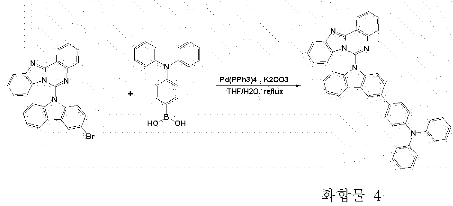
질소 분위기에서 500ml 둥근 바닥 플라스크에 화합물 A (10g, 21.6mmol), (4-(디페닐아미노)페닐)보론산 (6.88g, 23.81mmol)을 테트라하이드로퓨란 200ml에 완전히 녹인 후 2M 탄산칼륨수용액(100ml)을 첨가하고, 테트라키스-(트리페닐포스핀)팔라듐(0.75g, 0.65mmol)을 넣은 후 3 시간 동안 가열 교반하였다. 상온으로 온도를 낮추고 물 층을 제거하고 무수황산마그네슘으로 건조한 후 감압농축 시키고 에탄올 300ml로 재결정하여 화합물 4 (11.31g, 83%)를 제조하였다.
MS[M+H]+= 628
<제조예 5> 화합물 5의 합성
Figure PCTKR2016006014-appb-I000136
화합물 A(10g, 21.6mmol), 카바졸(4.01g, 23.81mmol) 그리고 NaOt-Bu (2.51g, 25.9mmol)을 톨루엔 200ml에 넣은 후 교반하면서 온도를 높였다. 승온한 후 환류되기 시작하면 비스(트리-tert-부틸포스핀)팔라듐(0.06g, 0.11mmol)을 천천히 떨어뜨리며 넣었다. 5시간 후 반응을 종료하여 온도를 상온으로 낮추고 감압 하에서 농축한 후 컬럼 정제하여 10.72g(90%)의 화합물 5를 제조하였다.
MS[M+H]+= 550
<제조예 6> 화합물 6의 합성
Figure PCTKR2016006014-appb-I000137
질소 분위기에서 500ml 둥근 바닥 플라스크에 화합물 A (10g, 21.6mmol), (4-(9H-카바졸-9-yl)페닐)보론산 (6.88g, 23.81mmol)을 테트라하이드로퓨란 280ml에 완전히 녹인 후 2M 탄산칼륨수용액(140ml)을 첨가하고, 테트라키스-(트리페닐포스핀)팔라듐(0.75g, 0.65mmol)을 넣은 후 6 시간 동안 가열 교반하였다. 상온으로 온도를 낮추고 물 층을 제거하고 무수황산마그네슘으로 건조한 후 감압농축 시키고 에틸아세테이트 200ml로 재결정하여 화합물 6 (10.31g, 78%)을 제조하였다.
MS[M+H]+= 626
<제조예 7> 화합물 7의 합성
Figure PCTKR2016006014-appb-I000138
질소 분위기에서 500ml 둥근 바닥 플라스크에 화합물 A (10g, 21.6mmol), (9-페닐-9H-카바졸-3-yl)보론산 (6.88g, 23.81mmol)을 테트라하이드로퓨란 300ml에 완전히 녹인 후 2M 탄산칼륨수용액(150ml)을 첨가하고, 테트라키스-(트리페닐포스핀)팔라듐(0.75g, 0.65mmol)을 넣은 후 2 시간 동안 가열 교반하였다. 상온으로 온도를 낮추고 물 층을 제거하고 무수황산마그네슘으로 건조한 후 감압농축 시키고 에틸아세테이트 200ml로 재결정하여 화합물 7 (12.09g, 91%)을 제조하였다.
MS[M+H]+= 626
<제조예 8> 화합물 8의 합성
Figure PCTKR2016006014-appb-I000139
질소 분위기에서 500ml 둥근 바닥 플라스크에 화합물 G (10g, 19.61mmol), 2-클로로-4,6-디페닐-1,3,5-트리아진 (4.76g, 17.83mmol)을 테트라하이드로퓨란 300ml에 완전히 녹인 후 2M 탄산칼륨수용액(150ml)을 첨가하고, 테트라키스-(트리페닐포스핀)팔라듐(0.62g, 0.53mmol)을 넣은 후 8 시간 동안 가열 교반하였다. 상온으로 온도를 낮추고 물 층을 제거하고 무수황산마그네슘으로 건조한 후 감압농축 시키고 에틸아세테이트 300ml로 재결정하여 화합물 8 (12.41g, 93%)을 제조하였다.
MS[M+H]+= 616
<제조예 9> 화합물 9의 합성
Figure PCTKR2016006014-appb-I000140
질소 분위기에서 500ml 둥근 바닥 플라스크에 화합물 G (10g, 19.61mmol), 2-클로로-4,6-디페닐피리미딘 (4.74g, 17.83mmol)을 테트라하이드로퓨란 300ml에 완전히 녹인 후 2M 탄산칼륨수용액(150ml)을 첨가하고, 테트라키스-(트리페닐포스핀)팔라듐(0.62g, 0.53mmol)을 넣은 후 5 시간 동안 가열 교반하였다. 상온으로 온도를 낮추고 물 층을 제거하고 무수황산마그네슘으로 건조한 후 감압농축 시키고 에틸아세테이트 250ml로 재결정하여 화합물 9 (10.15g, 78%)를 제조하였다.
MS[M+H]+= 615
<제조예 10> 화합물 10의 합성
Figure PCTKR2016006014-appb-I000141
질소 분위기에서 500ml 둥근 바닥 플라스크에 화합물 G (10g, 19.61mmol), 4-클로로-2,6-디페닐피리미딘 (4.74g, 17.83mmol)을 테트라하이드로퓨란 300ml에 완전히 녹인 후 2M 탄산칼륨수용액(150ml)을 첨가하고, 테트라키스-(트리페닐포스핀)팔라듐(0.62g, 0.53mmol)을 넣은 후 4 시간 동안 가열 교반하였다. 상온으로 온도를 낮추고 물 층을 제거하고 무수황산마그네슘으로 건조한 후 감압농축 시키고 에틸아세테이트 250ml로 재결정하여 화합물 10 (11.32g, 86%)을 제조하였다.
MS[M+H]+= 615
<제조예 11> 화합물 11의 합성
Figure PCTKR2016006014-appb-I000142
질소 분위기에서 500ml 둥근 바닥 플라스크에 화합물 G (10g, 19.61mmol), 2-클로로-4,6-디페닐피리미딘 (4.71g, 17.83mmol)을 테트라하이드로퓨란 300ml에 완전히 녹인 후 2M 탄산칼륨수용액(150ml)을 첨가하고, 테트라키스-(트리페닐포스핀)팔라듐(0.62g, 0.53mmol)을 넣은 후 2 시간 동안 가열 교반하였다. 상온으로 온도를 낮추고 물 층을 제거하고 무수황산마그네슘으로 건조한 후 감압농축 시키고 에틸아세테이트 280ml로 재결정하여 화합물 11 (11.32g, 86%)을 제조하였다.
MS[M+H]+= 614
<제조예 12> 화합물 12의 합성
Figure PCTKR2016006014-appb-I000143
질소 분위기에서 500ml 둥근 바닥 플라스크에 화합물 G (10g, 19.61mmol), 2-(4-브로모페닐)-4,6-디페닐-1,3,5-트리아진 (6.91g, 17.83mmol)을 테트라하이드로퓨란 400ml에 완전히 녹인 후 2M 탄산칼륨수용액(200ml)을 첨가하고, 테트라키스-(트리페닐포스핀)팔라듐(1.24g, 1.06mmol)을 넣은 후 12 시간 동안 가열 교반하였다. 상온으로 온도를 낮추고 물 층을 제거하고 무수황산마그네슘으로 건조한 후 감압농축 시키고 에틸아세테이트 500ml로 재결정하여 화합물 12 (12.41g, 93%)를 제조하였다.
MS[M+H]+= 692
<제조예 13> 화합물 13의 합성
Figure PCTKR2016006014-appb-I000144
질소 분위기에서 500ml 둥근 바닥 플라스크에 화합물 G (10g, 19.61mmol), 2-(3-브로모페닐)-4,6-디페닐-1,3,5-트리아진 (6.91g, 17.83mmol)을 테트라하이드로퓨란 400ml에 완전히 녹인 후 2M 탄산칼륨수용액(200ml)을 첨가하고, 테트라키스-(트리페닐포스핀)팔라듐(1.24g, 1.06mmol)을 넣은 후 7 시간 동안 가열 교반하였다. 상온으로 온도를 낮추고 물 층을 제거하고 무수황산마그네슘으로 건조한 후 감압농축 시키고 에틸아세테이트 400ml로 재결정하여 화합물 13 (9.55g, 64%)을 제조하였다.
MS[M+H]+= 693
<제조예 14> 화합물 14의 합성
Figure PCTKR2016006014-appb-I000145
질소 분위기에서 500ml 둥근 바닥 플라스크에 화합물 A (10g, 21.6mmol), 디벤조bs,d]퓨란-2-일보론산 (5.26g, 23.81mmol)을 테트라하이드로퓨란 300ml에 완전히 녹인 후 2M 탄산칼륨수용액(150ml)을 첨가하고, 테트라키스-(트리페닐포스핀)팔라듐(0.75g, 0.65mmol)을 넣은 후 6 시간 동안 가열 교반하였다. 상온으로 온도를 낮추고 물 층을 제거하고 무수황산마그네슘으로 건조한 후 감압농축 시키고 에틸아세테이트 300ml로 재결정하여 화합물 14 (10.82g, 91%)를 제조하였다.
MS[M+H]+= 551
<제조예 15> 화합물 15의 합성
Figure PCTKR2016006014-appb-I000146
질소 분위기에서 500ml 둥근 바닥 플라스크에 화합물 A (10g, 21.6mmol), 디벤조[b,d]티오펜-2-일보론산 (5.32g, 23.81mmol)을 테트라하이드로퓨란 300ml에 완전히 녹인 후 2M 탄산칼륨수용액(150ml)을 첨가하고, 테트라키스-(트리페닐포스핀)팔라듐(0.75g, 0.65mmol)을 넣은 후 5 시간 동안 가열 교반하였다. 상온으로 온도를 낮추고 물 층을 제거하고 무수황산마그네슘으로 건조한 후 감압농축 시키고 에틸아세테이트 200ml로 재결정하여 화합물 15 (9.44g, 80%)를 제조하였다.
MS[M+H]+= 567
<제조예 16> 화합물 16의 합성
Figure PCTKR2016006014-appb-I000147
질소 분위기에서 500ml 둥근 바닥 플라스크에 화합물 A (10g, 21.6mmol), [1,1':3',1"-터페닐]-5'-일보론산 (6.52g, 23.81mmol)을 테트라하이드로퓨란 300ml에 완전히 녹인 후 2M 탄산칼륨수용액(150ml)을 첨가하고, 테트라키스-(트리페닐포스핀)팔라듐(0.75g, 0.65mmol)을 넣은 후 6 시간 동안 가열 교반하였다. 상온으로 온도를 낮추고 물 층을 제거하고 무수황산마그네슘으로 건조한 후 감압농축 시키고 에틸아세테이트 200ml로 재결정하여 화합물 16 (10.42g, 78%)을 제조하였다.
MS[M+H]+= 613
<제조예 17> 화합물 17의 합성
Figure PCTKR2016006014-appb-I000148
질소 분위기에서 500ml 둥근 바닥 플라스크에 화합물 A (10g, 21.6mmol), (9,9-디메틸-9H-플루오렌-2-일)보론산 (5.66g, 23.81mmol)을 테트라하이드로퓨란 320ml에 완전히 녹인 후 2M 탄산칼륨수용액(160ml)을 첨가하고, 테트라키스-(트리페닐포스핀)팔라듐(0.75g, 0.65mmol)을 넣은 후 3 시간 동안 가열 교반하였다. 상온으로 온도를 낮추고 물 층을 제거하고 무수황산마그네슘으로 건조한 후 감압농축 시키고 에틸아세테이트 200ml로 재결정하여 화합물 17 (9.56g, 76%)을 제조하였다.
MS[M+H]+= 577
<제조예 18> 화합물 18의 합성
Figure PCTKR2016006014-appb-I000149
질소 분위기에서 500ml 둥근 바닥 플라스크에 화합물 A (10g, 21.6mmol), (4-(나프탈렌-2-일)페닐)보론산 (6.51g, 23.81mmol)을 테트라하이드로퓨란 320ml에 완전히 녹인 후 2M 탄산칼륨수용액(160ml)을 첨가하고, 테트라키스-(트리페닐포스핀)팔라듐(0.75g, 0.65mmol)을 넣은 후 5 시간 동안 가열 교반하였다. 상온으로 온도를 낮추고 물 층을 제거하고 무수황산마그네슘으로 건조한 후 감압농축 시키고 에틸아세테이트 300ml로 재결정하여 화합물 18 (10.22g, 84%)을 제조하였다.
MS[M+H]+= 587
<제조예 19> 화합물 19의 합성
Figure PCTKR2016006014-appb-I000150
질소 분위기에서 500ml 둥근 바닥 플라스크에 화합물 A (10g, 21.6mmol), 9,9'-스피로비[플루오렌]-2-일보론산 (8.57g, 23.81mmol)을 테트라하이드로퓨란 400ml에 완전히 녹인 후 2M 탄산칼륨수용액(200ml)을 첨가하고, 테트라키스-(트리페닐포스핀)팔라듐(0.75g, 0.65mmol)을 넣은 후 5 시간 동안 가열 교반하였다. 상온으로 온도를 낮추고 물 층을 제거하고 무수황산마그네슘으로 건조한 후 감압농축 시키고 에틸아세테이트 300ml로 재결정하여 화합물 19 (13.74g, 91%)를 제조하였다.
MS[M+H]+= 699
<제조예 20> 화합물 20의 합성
Figure PCTKR2016006014-appb-I000151
질소 분위기에서 500ml 둥근 바닥 플라스크에 화합물 A (10g, 21.6mmol), (4-(1-페닐-1H-benzo[d]이미다졸-2-일)페닐)보론산 (7.48g, 23.81mmol)을 테트라하이드로퓨란 300ml에 완전히 녹인 후 2M 탄산칼륨수용액(140ml)을 첨가하고, 테트라키스-(트리페닐포스핀)팔라듐(0.75g, 0.65mmol)을 넣은 후 8 시간 동안 가열 교반하였다. 상온으로 온도를 낮추고 물 층을 제거하고 무수황산마그네슘으로 건조한 후 감압농축 시키고 에틸아세테이트 200ml로 재결정하여 화합물 20 (12.42g, 87%)을 제조하였다.
MS[M+H]+= 653
<제조예 21> 화합물 21의 합성
Figure PCTKR2016006014-appb-I000152
질소 분위기에서 500ml 둥근 바닥 플라스크에 화합물 A (10g, 21.6mmol), (4-(벤조[d]옥사졸-2-일)페닐)보론산 (5.69g, 23.81mmol)을 테트라하이드로퓨란 300ml에 완전히 녹인 후 2M 탄산칼륨수용액(140ml)을 첨가하고, 테트라키스-(트리페닐포스핀)팔라듐(0.75g, 0.65mmol)을 넣은 후 3 시간 동안 가열 교반하였다. 상온으로 온도를 낮추고 물 층을 제거하고 무수황산마그네슘으로 건조한 후 감압농축 시키고 에틸아세테이트 200ml로 재결정하여 화합물 21 (10.11g, 81%)을 제조하였다.
MS[M+H]+= 578
<제조예 22> 화합물 22의 합성
Figure PCTKR2016006014-appb-I000153
질소 분위기에서 500ml 둥근 바닥 플라스크에 화합물 A (10g, 21.6mmol), (4-(벤조[d]티아졸-2-일)페닐)보론산 (5.69g, 23.81mmol)을 테트라하이드로퓨란 300ml에 완전히 녹인 후 2M 탄산칼륨수용액(140ml)을 첨가하고, 테트라키스-(트리페닐포스핀)팔라듐(0.75g, 0.65mmol)을 넣은 후 3 시간 동안 가열 교반하였다. 상온으로 온도를 낮추고 물 층을 제거하고 무수황산마그네슘으로 건조한 후 감압농축 시키고 에틸아세테이트 200ml로 재결정하여 화합물 22 (9.53g, 74%)를 제조하였다.
MS[M+H]+= 594
<제조예 23> 화합물 23의 합성
Figure PCTKR2016006014-appb-I000154
질소 분위기에서 500ml 둥근 바닥 플라스크에 화합물 A (10g, 21.6mmol), (4-(벤조[d]티아졸-2-일)페닐)보론산 (6.84g, 23.81mmol)을 테트라하이드로퓨란 300ml에 완전히 녹인 후 2M 탄산칼륨수용액(140ml)을 첨가하고, 테트라키스-(트리페닐포스핀)팔라듐(0.75g, 0.65mmol)을 넣은 후 2 시간 동안 가열 교반하였다. 상온으로 온도를 낮추고 물 층을 제거하고 무수황산마그네슘으로 건조한 후 감압농축 시키고 에틸아세테이트 200ml로 재결정하여 화합물 23 (9.53g, 74%)을 제조하였다.
MS[M+H]+= 662
<제조예 24> 화합물 24 내지 46의 합성
제조예 1 내지 23 에서 출발물질을 화합물 A 대신 화합물 B를 사용하고, 화합물 G 대신 화합물 H를 사용한 것을 제외하고, 상기 화합물 1 내지 23을 제조하는 방법과 동일하게 하기 화합물 24 내지 46을 제조하였다.
Figure PCTKR2016006014-appb-I000155
Figure PCTKR2016006014-appb-I000156
Figure PCTKR2016006014-appb-I000157
<제조예 25> 화합물 47 내지 69의 합성
제조예 1 내지 23 에서 출발물질을 화합물 A 대신 화합물 E 를 사용한 것을 제외하고, 상기 화합물 1 내지 23을 제조하는 방법과 동일하게 하기 화합물 47 내지 69를 제조하였다.
Figure PCTKR2016006014-appb-I000158
Figure PCTKR2016006014-appb-I000159
Figure PCTKR2016006014-appb-I000160
<제조예 26> 화합물 70 내지 92의 합성
제조예 1 내지 23 에서 출발물질을 화합물 A 대신 화합물 F 를 사용한 것을 제외하고, 상기 화합물 1 내지 23을 제조하는 방법과 동일하게 하기 화합물 70 내지 92를 제조하였다.
Figure PCTKR2016006014-appb-I000161
Figure PCTKR2016006014-appb-I000162
Figure PCTKR2016006014-appb-I000163
<제조예 27> 화합물 93의 합성
Figure PCTKR2016006014-appb-I000164
화합물 C(10g, 18.52mmol), 디페닐아민(6.88g, 40.74mmol) 그리고 NaOt-Bu (4.62g, 48.2mmol)을 톨루엔 200ml에 넣은 후 교반하면서 온도를 높였다. 승온한 후 환류되기 시작하면 비스(트리-tert-부틸포스핀)팔라듐(0.09g, 0.18mmol)을 천천히 떨어뜨리며 넣었다. 5시간 후 반응을 종료하여 온도를 상온으로 낮추고 감압 하에서 농축한 후 컬럼 정제하여 10.42g(80%)의 화합물 93을 제조하였다.
MS[M+H]+= 719
<제조예 28> 화합물 94의 합성
Figure PCTKR2016006014-appb-I000165
화합물 C(10g, 18.52mmol), 카바졸(6.85g, 40.74mmol) 그리고 NaOt-Bu (4.62g, 48.2mmol)을 톨루엔 200ml에 넣은 후 교반하면서 온도를 높였다. 승온한 후 환류되기 시작하면 비스(트리-tert-부틸포스핀)팔라듐(0.09g, 0.18mmol)을 천천히 떨어뜨리며 넣었다. 5시간 후 반응을 종료하여 온도를 상온으로 낮추고 감압 하에서 농축한 후 컬럼 정제하여 8.42g(71%)의 화합물 94를 제조하였다.
MS[M+H]+= 715
<제조예 29> 화합물 95의 합성
Figure PCTKR2016006014-appb-I000166
질소 분위기에서 500ml 둥근 바닥 플라스크에 화합물 C(10g, 18.52mmol), (4-(디페닐아미노)페닐)보론산 (11.40g, 40.74mmol)을 테트라하이드로퓨란 320ml에 완전히 녹인 후 2M 탄산칼륨수용액(110ml)을 첨가하고, 테트라키스-(트리페닐포스핀)팔라듐(0.65g, 0.56mmol)을 넣은 후 3 시간 동안 가열 교반하였다. 상온으로 온도를 낮추고 물 층을 제거하고 무수황산마그네슘으로 건조한 후 감압농축 시키고 에틸아세테이트 200ml로 재결정하여 화합물 95 (13.54g, 84%)를 제조하였다.
MS[M+H]+= 871
<제조예 30> 화합물 96의 합성
Figure PCTKR2016006014-appb-I000167
질소 분위기에서 500ml 둥근 바닥 플라스크에 화합물 C(10g, 18.52mmol), 나프탈렌-일보론산 (7.01g, 40.74mmol)을 테트라하이드로퓨란 280ml에 완전히 녹인 후 2M 탄산칼륨수용액(120ml)을 첨가하고, 테트라키스-(트리페닐포스핀)팔라듐(0.65g, 0.56mmol)을 넣은 후 1 시간 동안 가열 교반하였다. 상온으로 온도를 낮추고 물 층을 제거하고 무수황산마그네슘으로 건조한 후 감압농축 시키고 에틸아세테이트 300ml로 재결정하여 화합물 96 (9.45g, 80%)을 제조하였다.
MS[M+H]+= 637
<제조예 31> 화합물 97의 합성
Figure PCTKR2016006014-appb-I000168
질소 분위기에서 500ml 둥근 바닥 플라스크에 화합물 C(10g, 18.52mmol), 디벤조[b,d]퓨란-4-일보론산 (8.64g, 40.74mmol)을 테트라하이드로퓨란 300ml에 완전히 녹인 후 2M 탄산칼륨수용액(150ml)을 첨가하고, 테트라키스-(트리페닐포스핀)팔라듐(0.65g, 0.56mmol)을 넣은 후 3 시간 동안 가열 교반하였다. 상온으로 온도를 낮추고 물 층을 제거하고 무수황산마그네슘으로 건조한 후 감압농축 시키고 에틸아세테이트 300ml로 재결정하여 화합물 97 (11.24g, 84%)을 제조하였다.
MS[M+H]+= 717
<제조예 32> 화합물 98의 합성
Figure PCTKR2016006014-appb-I000169
질소 분위기에서 500ml 둥근 바닥 플라스크에 화합물 C(10g, 18.52mmol), 디벤조[b,d]퓨란-4-일보론산 (13.12g, 40.74mmol)을 테트라하이드로퓨란 360ml에 완전히 녹인 후 2M 탄산칼륨수용액(180ml)을 첨가하고, 테트라키스-(트리페닐포스핀)팔라듐(0.65g, 0.56mmol)을 넣은 후 15 시간 동안 가열 교반하였다. 상온으로 온도를 낮추고 물 층을 제거하고 무수황산마그네슘으로 건조한 후 감압농축 시키고 에틸아세테이트 300ml로 재결정하여 화합물 98 (14.15g, 81%)을 제조하였다.
MS[M+H]+= 937
<제조예 33> 화합물 99 내지 104의 합성
제조예 27 내지 32 에서 출발물질을 화합물 C 대신 화합물 D 를 사용한 것을 제외하고, 상기 화합물 93 내지 98을 제조하는 방법과 동일하게 하기 화합물 99 내지 104를 제조하였다.
Figure PCTKR2016006014-appb-I000170
<실험예 1-1>
ITO(indium tin oxide)가 1,000Å의 두께로 박막 코팅된 유리 기판을 세제를 녹인 증류수에 넣고 초음파로 세척하였다. 이 때, 세제로는 피셔사(Fischer Co.) 제품을 사용하였으며, 증류수로는 밀러포어사(Millipore Co.) 제품의 필터(Filter)로 2차로 걸러진 증류수를 사용하였다. ITO를 30분간 세척한 후 증류수로 2회 반복하여 초음파 세척을 10분간 진행하였다. 증류수 세척이 끝난 후, 이소프로필알콜, 아세톤, 메탄올의 용제로 초음파 세척을 하고 건조시킨 후 플라즈마 세정기로 수송시켰다. 또한, 산소 플라즈마를 이용하여 상기 기판을 5분간 세정한 후 진공 증착기로 기판을 수송시켰다.
이렇게 준비된 ITO 투명 전극 위에 하기 화학식의 헥사니트릴 헥사아자트리페닐렌 (hexaazatriphenylene; HAT)를 500Å의 두께로 열 진공 증착하여 정공 주입층을 형성하였다.
[HAT]
Figure PCTKR2016006014-appb-I000171
상기 정공 주입층 위에 정공을 수송하는 물질인 하기 화합물 4-4'-비스[N-(1-나프틸)-N-페닐아미노]비페닐(NPB)(300Å)를 진공 증착하여 정공 수송층을 형성하였다.
[NPB]
Figure PCTKR2016006014-appb-I000172
이어서, 상기 정공 수송층 위에 막 두께 100Å으로 하기 화합물 1을 진공 증착하여 전자 저지층을 형성하였다.
[화합물 1]
Figure PCTKR2016006014-appb-I000173
이어서, 상기 전자 저지층 위에 막 두께 300Å으로 아래와 같은 BH와 BD를 25:1의 중량비로 진공증착하여 발광층을 형성하였다.
[BH]
Figure PCTKR2016006014-appb-I000174
[BD]
Figure PCTKR2016006014-appb-I000175
[ET1]
Figure PCTKR2016006014-appb-I000176
[LiQ]
Figure PCTKR2016006014-appb-I000177
상기 발광층 위에 상기 화합물 ET1과 상기 화합물 LiQ(Lithium Quinolate)를 1:1의 중량비로 진공증착하여 300Å의 두께로 전자 주입 및 수송층을 형성하였다. 상기 전자 주입 및 수송층 위에 순차적으로 12Å두께로 리튬플로라이드(LiF)와 2,000Å 두께로 알루미늄을 증착하여 음극을 형성하였다.
상기의 과정에서 유기물의 증착속도는 0.4~ 0.7Å/sec를 유지하였고, 음극의 리튬플로라이드는 0.3Å/sec, 알루미늄은 2Å/sec의 증착 속도를 유지하였으며, 증착시 진공도는 2 × 10⁻⁷ ~5 × 10⁻⁶ torr를 유지하여, 유기 발광 소자를 제작하였다.
<실험예 1-2>
상기 실험예 1-1에서 화합물 1 대신 상기 화합물 2를 사용한 것을 제외하고는 실험예 1-1과 동일한 방법으로 유기 발광 소자를 제작하였다.
<실험예 1-3>
상기 실험예 1-1에서 화합물 1 대신 상기 화합물 3을 사용한 것을 제외하고는 실험예 1-1과 동일한 방법으로 유기 발광 소자를 제작하였다.
<실험예 1-4>
상기 실험예 1-1에서 화합물 1 대신 상기 화합물 4를 사용한 것을 제외하고는 실험예 1-1과 동일한 방법으로 유기 발광 소자를 제작하였다.
<실험예 1-5>
상기 실험예 1-1에서 화합물 1 대신 상기 화합물 5를 사용한 것을 제외하고는 실험예 1-1과 동일한 방법으로 유기 발광 소자를 제작하였다.
<실험예 1-6>
상기 실험예 1-1에서 화합물 1 대신 상기 화합물 6을 사용한 것을 제외하고는 실험예 1-1과 동일한 방법으로 유기 발광 소자를 제작하였다.
<실험예 1-7>
상기 실험예 1-1에서 화합물1 대신 상기 화합물 7을 사용한 것을 제외하고는 실험예 1-1과 동일한 방법으로 유기 발광 소자를 제작하였다.
<실험예 1-8>
상기 실험예 1-1에서 화합물 1 대신 상기 화합물 24를 사용한 것을 제외하고는 실험예 1-1과 동일한 방법으로 유기 발광 소자를 제작하였다.
<실험예 1-9>
상기 실험예 1-1에서 화합물 1 대신 상기 화합물 25를 사용한 것을 제외하고는 실험예 1-1과 동일한 방법으로 유기 발광 소자를 제작하였다.
<실험예 1-10>
상기 실험예 1-1에서 화합물 1 대신 상기 화합물 26을 사용한 것을 제외하고는 실험예 1-1과 동일한 방법으로 유기 발광 소자를 제작하였다.
<실험예 1-11>
상기 실험예 1-1에서 화합물 1 대신 상기 화합물 27를 사용한 것을 제외하고는 실험예 1-1과 동일한 방법으로 유기 발광 소자를 제작하였다.
<실험예 1-12>
상기 실험예 1-1에서 화합물 1 대신 상기 화합물 28를 사용한 것을 제외하고는 실험예 1-1과 동일한 방법으로 유기 발광 소자를 제작하였다.
<실험예 1-13>
상기 실험예 1-1에서 화합물 1 대신 상기 화합물 29를 사용한 것을 제외하고는 실험예 1-1과 동일한 방법으로 유기 발광 소자를 제작하였다.
<실험예 1-14>
상기 실험예 1-1에서 화합물 1 대신 상기 화합물 30를 사용한 것을 제외하고는 실험예 1-1과 동일한 방법으로 유기 발광 소자를 제작하였다.
<실험예 1-15>
상기 실험예1-1에서 화합물 1 대신 상기 화합물 47를 사용한 것을 제외하고는 실험예 1-1과 동일한 방법으로 유기 발광 소자를 제작하였다.
<실험예 1-16>
상기 실험예 1-1에서 화합물 1 대신 상기 화합물 48을 사용한 것을 제외하고는 실험예 1-1과 동일한 방법으로 유기 발광 소자를 제작하였다.
<실험예 1-17>
상기 실험예 1-1에서 화합물 1 대신 상기 화합물 49를 사용한 것을 제외하고는 실험예 1-1과 동일한 방법으로 유기 발광 소자를 제작하였다.
<실험예 1-18>
상기 실험예 1-1에서 화합물 1 대신 상기 화합물 50을 사용한 것을 제외하고는 실험예 1-1과 동일한 방법으로 유기 발광 소자를 제작하였다.
<실험예 1-19>
상기 실험예 1-1에서 화합물 1 대신 상기 화합물 51를 사용한 것을 제외하고는 실험예 1-1과 동일한 방법으로 유기 발광 소자를 제작하였다.
<실험예 1-20>
상기 실험예 1-1에서 화합물 1 대신 상기 화합물 52를 사용한 것을 제외하고는 실험예 1-1과 동일한 방법으로 유기 발광 소자를 제작하였다.
<실험예 1-21>
상기 실험예 1-1에서 화합물 1 대신 상기 화합물 53을 사용한 것을 제외하고는 실험예 1-1과 동일한 방법으로 유기 발광 소자를 제작하였다.
<실험예 1-22>
상기 실험예 1-1에서 화합물 1 대신 상기 화합물 70를 사용한 것을 제외하고는 실험예 1-1과 동일한 방법으로 유기 발광 소자를 제작하였다.
<실험예 1-23>
상기 실험예 1-1에서 화합물 1 대신 상기 화합물 71을 사용한 것을 제외하고는 실험예 1-1과 동일한 방법으로 유기 발광 소자를 제작하였다.
<실험예 1-24>
상기 실험예 1-1에서 화합물 1 대신 상기 화합물 72를 사용한 것을 제외하고는 실험예 1-1과 동일한 방법으로 유기 발광 소자를 제작하였다.
<실험예 1-25>
상기 실험예 1-1에서 화합물 1 대신 상기 화합물 73를 사용한 것을 제외하고는 실험예 1-1과 동일한 방법으로 유기 발광 소자를 제작하였다.
<실험예 1-26>
상기 실험예 1-1에서 화합물 1 대신 상기 화합물 74를 사용한 것을 제외하고는 실험예 1-1과 동일한 방법으로 유기 발광 소자를 제작하였다.
<실험예 1-27>
상기 실험예 1-1에서 화합물 1 대신 상기 화합물 75를 사용한 것을 제외하고는 실험예 1-1과 동일한 방법으로 유기 발광 소자를 제작하였다.
<실험예 1-28>
상기 실험예 1-1에서 화합물 1 대신 상기 화합물 76를 사용한 것을 제외하고는 실험예 1-1과 동일한 방법으로 유기 발광 소자를 제작하였다.
<실험예 1-29>
상기 실험예 1-1에서 화합물 1 대신 상기 화합물 93를 사용한 것을 제외하고는 실험예 1-1과 동일한 방법으로 유기 발광 소자를 제작하였다.
<실험예 1-30>
상기 실험예 1-1에서 화합물 1 대신 상기 화합물 94를 사용한 것을 제외하고는 실험예 1-1과 동일한 방법으로 유기 발광 소자를 제작하였다.
<실험예 1-31>
상기 실험예 1-1에서 화합물 1 대신 상기 화합물 95를 사용한 것을 제외하고는 실험예 1-1과 동일한 방법으로 유기 발광 소자를 제작하였다.
<실험예 1-32>
상기 실험예 1-1에서 화합물 1 대신 상기 화합물 99를 사용한 것을 제외하고는 실험예 1-1과 동일한 방법으로 유기 발광 소자를 제작하였다.
<실험예 1-33>
상기 실험예 1-1에서 화합물 1 대신 상기 화합물 100를 사용한 것을 제외하고는 실험예 1-1과 동일한 방법으로 유기 발광 소자를 제작하였다.
<실험예 1-34>
상기 실험예 1-1에서 화합물 1 대신 상기 화합물 101를 사용한 것을 제외하고는 실험예 1-1과 동일한 방법으로 유기 발광 소자를 제작하였다.
<비교예 1-1>
상기 실험예 1-1에서 화합물 1 대신 하기 화합물 EB 1(TCTA)를 사용한 것을 제외하고는 실험예 1-1과 동일한 방법으로 유기 발광 소자를 제작하였다.
[EB 1]
Figure PCTKR2016006014-appb-I000178
<비교예 1-2>
상기 실험예 1-1에서 화합물 1 대신 하기 화합물 EB 2를 사용한 것을 제외하고는 실험예 1-1과 동일한 방법으로 유기 발광 소자를 제작하였다.
[EB 2]
Figure PCTKR2016006014-appb-I000179
<비교예 1-3>
상기 실험예 1-1에서 화합물 1 대신 하기 화합물 EB 3를 사용한 것을 제외하고는 실험예 1-1과 동일한 방법으로 유기 발광 소자를 제작하였다.
[EB 3]
Figure PCTKR2016006014-appb-I000180
<비교예 1-4>
상기 실험예 1-1에서 화합물 1 대신 하기 화합물 EB 4를 사용한 것을 제외하고는 실험예 1-1과 동일한 방법으로 유기 발광 소자를 제작하였다.
[EB 4]
Figure PCTKR2016006014-appb-I000181
실험예 1-1 내지 1-34 및 비교예 1-1 및 1-4에 의해 제작된 유기 발광 소자에 전류를 인가하였을 때, 성능평가를 하기 표 1에 나타내었다.
화합물(전자억제층) 전압(V@10mA/cm2) 효율(cd/A@10mA/cm2) 색좌표(x,y)
실험예 1-1 화합물 1 3.75 5.85 (0.139, 0.122)
실험예 1-2 화합물 2 3.72 5.88 (0.138, 0.126)
실험예 1-3 화합물 3 3.77 5.81 (0.138, 0.127)
실험예 1-4 화합물 4 3.78 5.82 (0.137, 0.125)
실험예 1-5 화합물 5 3.79 5.83 (0.136, 0.125)
실험예 1-6 화합물 6 3.74 5.87 (0.136, 0.127)
실험예 1-7 화합물 7 3.73 5.88 (0.136, 0.125)
실험예 1-8 화합물 24 3.74 5.71 (0.137, 0.125)
실험예 1-9 화합물 25 3.73 5.78 (0.138, 0.125)
실험예 1-10 화합물 26 3.74 5.62 (0.136, 0.125)
실험예 1-11 화합물 27 3.73 5.77 (0.137, 0.125)
실험예 1-12 화합물 28 3.85 5.75 (0.136, 0.125)
실험예 1-13 화합물 29 3.82 5.68 (0.138, 0.126)
실험예 1-14 화합물 30 3.87 5.71 (0.137, 0.125)
실험예 1-15 화합물 47 3.88 5.72 (0.136, 0.127)
실험예 1-16 화합물 48 3.89 5.73 (0.135, 0.127)
실험예 1-17 화합물 49 3.84 5.77 (0.138, 0.127)
실험예 1-18 화합물 50 3.83 5.78 (0.137, 0.125)
실험예 1-19 화합물 51 3.84 5.71 (0.137, 0.125)
실험예 1-20 화합물 52 3.83 5.78 (0.136, 0.127)
실험예 1-21 화합물 53 3.84 5.72 (0.135, 0.127)
실험예 1-22 화합물 70 3.83 5.77 (0.138, 0.127)
실험예 1-23 화합물 71 3.89 5.75 (0.137, 0.125)
실험예 1-24 화합물 72 3.88 5.78 (0.137, 0.125)
실험예 1-25 화합물 73 3.87 5.71 (0.136, 0.125)
실험예 1-26 화합물 74 3.61 5.65 (0.139, 0.122)
실험예 1-27 화합물 75 3.63 5.68 (0.138, 0.126)
실험예 1-28 화합물 76 3.62 5.61 (0.138, 0.127)
실험예 1-29 화합물 93 3.74 5.62 (0.137, 0.125)
실험예 1-30 화합물 94 3.70 5.63 (0.136, 0.125)
실험예 1-31 화합물 95 3.75 5.67 (0.136, 0.127)
실험예 1-32 화합물 99 3.80 5.58 (0.136, 0.125)
실험예 1-33 화합물 100 3.84 5.51 (0.137, 0.125)
실험예 1-34 화합물 101 3.82 5.54 (0.138, 0.125)
비교예 1-1 EB1 4.37 4.68 (0.138, 0.125)
비교예 1-2 EB2 4.15 4.85 (0.138, 0.125)
비교예 1-3 EB3 4.63 4.32 (0.138, 0.126)
비교예 1-4 EB4 4.52 4.41 (0.138, 0.125)
상기 표 1에서 나타난 바와 같이, 실험예 1-1 내지 1-34의 화합물로 이루어진 유기발광소자는 전자억제층으로 자주 사용되는 TCTA(비교예 1-1), 비교예 1-2, -L-Ar이 페닐기인 비교예 1-3 및 이미다조 퀴나졸린과 카바졸 사이에 링커로 나프탈렌이 연결된 비교예 1-4 보다 저전압, 고효율의 특성을 나타내는 것을 알 수 있다. 특히 화합물 A로부터 제조된 화합물 1 내지 7을 사용한 유기 발광 소자에서 저전압 고효율 특성이 가장 뛰어난 것을 알 수 있다.
따라서, 본 출원에 따른 화학식의 화합물 유도체는 전자 억제 능력이 우수하여 저전압 및 고효율의 특성을 보이며 유기 발광 소자에 적용 가능함을 확인할 수 있었다.
<실험예 2>
<실험예 2-1 내지 실험예 2-34>
상기 실험예 1에서 전자 저지층으로 TCTA을 사용하고, 정공 수송층으로 NPB 대신 실험예 1-1 내지 1-34의 화합물들을 사용한 것을 제외하고는 동일하게 실험하였다.
<비교예 2-1>
상기 실험예 1에서 전자 저지층으로 TCTA을 사용하고, 정공 수송층으로 HT 1(NPB)을 사용한 것을 제외하고는 동일하게 실험하였다.
<비교예 2-2>
상기 실험예 1에서 전자 저지층으로 TCTA을 사용하고, 정공 수송층으로 HT 2를 사용한 것을 제외하고는 동일하게 실험하였다.
[HT 2]
Figure PCTKR2016006014-appb-I000182
<비교예 2-3>
상기 실험예 1에서 전자 저지층으로 TCTA을 사용하고, 정공 수송층으로 HT 3를 사용한 것을 제외하고는 동일하게 실험하였다.
[HT 3]
Figure PCTKR2016006014-appb-I000183
<비교예 2-4>
상기 실험예 1에서 전자 저지층으로 TCTA을 사용하고, 정공 수송층으로 HT 4를 사용한 것을 제외하고는 동일하게 실험하였다.
[HT 4]
Figure PCTKR2016006014-appb-I000184
실험예 2-1 내지 2-25 및 비교예 2-1 및 2-4에 의해 제작된 유기 발광 소자에 전류를 인가하였을 때, 성능평가를 하기 표 2에 나타내었다.
화합물(정공수송층) 전압(V@10mA/cm2) 효율(cd/A@10mA/cm2) 색좌표(x,y)
실험예 2-1 화합물 1 4.35 5.95 (0.139, 0.122)
실험예 2-2 화합물 2 4.32 5.98 (0.138, 0.126)
실험예 2-3 화합물 3 4.37 5.91 (0.138, 0.127)
실험예 2-4 화합물 4 4.38 5.92 (0.137, 0.125)
실험예 2-5 화합물 5 4.39 5.93 (0.136, 0.125)
실험예 2-6 화합물 6 4.34 5.97 (0.136, 0.127)
실험예 2-7 화합물 7 4.33 5.98 (0.136, 0.125)
실험예 2-8 화합물 24 4.34 5.91 (0.137, 0.125)
실험예 2-9 화합물 25 4.33 5.98 (0.138, 0.125)
실험예 2-10 화합물 26 4.34 5.92 (0.136, 0.125)
실험예 2-11 화합물 27 4.33 5.97 (0.137, 0.125)
실험예 2-12 화합물 28 4.45 5.85 (0.136, 0.125)
실험예 2-13 화합물 29 4.42 5.88 (0.138, 0.126)
실험예 2-14 화합물 30 4.47 5.81 (0.137, 0.125)
실험예 2-15 화합물 47 4.48 5.82 (0.136, 0.127)
실험예 2-16 화합물 48 4.49 5.83 (0.135, 0.127)
실험예 2-17 화합물 49 4.44 5.87 (0.138, 0.127)
실험예 2-18 화합물 50 4.43 5.88 (0.137, 0.125)
실험예 2-19 화합물 51 4.44 5.81 (0.137, 0.125)
실험예 2-20 화합물 52 4.43 5.88 (0.136, 0.127)
실험예 2-21 화합물 53 4.44 5.82 (0.135, 0.127)
실험예 2-22 화합물 70 4.43 5.87 (0.138, 0.127)
실험예 2-23 화합물 71 4.59 5.75 (0.137, 0.125)
실험예 2-24 화합물 72 4.48 5.88 (0.137, 0.125)
실험예 2-25 화합물 73 4.37 5.94 (0.136, 0.125)
실험예 2-26 화합물 74 4.35 5.95 (0.139, 0.122)
실험예 2-27 화합물 75 4.32 5.98 (0.138, 0.126)
실험예 2-28 화합물 76 4.37 5.91 (0.138, 0.127)
실험예 2-29 화합물 93 4.58 5.82 (0.137, 0.125)
실험예 2-30 화합물 94 4.59 5.83 (0.136, 0.125)
실험예 2-31 화합물 95 4.54 5.87 (0.136, 0.127)
실험예 2-32 화합물 99 4.53 5.88 (0.136, 0.125)
실험예 2-33 화합물 100 4.54 5.81 (0.137, 0.125)
실험예 2-34 화합물 101 4.53 5.88 (0.138, 0.125)
비교예 2-1 HT1 5.85 4.12 (0.136, 0.125)
비교예 2-2 HT2 5.63 4.37 (0.137, 0.125)
비교예 2-3 HT3 5.72 4.25 (0.136, 0.126)
비교예 2-4 HT4 5.56 4.43 (0.137, 0.126)
상기 표 2에서 나타난 바와 같이, 실험예 2-1 내지 2-34의 화합물로 이루어진 유기발광소자는 정공수송층으로 자주 사용되는 NPB(비교예 2-1), 비교예 2-2, -L-Ar이 페닐기인 비교예 2-3 및 이미다조 퀴나졸린과 카바졸 사이에 링커로 나프탈렌이 연결된 비교예 2-4 보다 저전압, 고효율의 특성을 나타내는 것을 알 수 있다. 특히 화합물 A로부터 제조된 화합물 1 내지 7을 사용한 유기 발광 소자에서 저전압 고효율 특성이 가장 뛰어난 것을 알 수 있다.
따라서, 본 출원에 따른 화학식의 화합물 유도체는 전자 억제 능력뿐만 아니라 정공 수송 능력 또한 우수하여 저전압 및 고효율의 특성을 보이며 유기 발광 소자에 적용 가능함을 확인할 수 있었다.
<실험예 3-1>
합성예 에서 합성된 화합물들을 통상적으로 알려진 방법으로 고순도 승화정제를 한 후, 하기와 같은 방법으로 녹색 유기 발광 소자를 제조하였다.
ITO(ndium tin oxide)가 1,000Å의 두께로 박막 코팅된 유리 기판을 세제를 녹인 증류수에 넣고 초음파로 세척하였다. 이 때, 세제로는 피셔사(Fischer Co.) 제품을 사용하였으며, 증류수로는 밀러포어사(Millipore Co.) 제품의 필터(Filter)로 2차로 걸러진 증류수를 사용하였다. ITO를 30분간 세척한 후 증류수로 2회 반복하여 초음파 세척을 10분간 진행하였다. 증류수 세척이 끝난 후, 이소프로필알콜, 아세톤, 메탄올의 용제로 초음파 세척을 하고 건조시킨 후 플라즈마 세정기로 수송시켰다. 또한, 산소 플라즈마를 이용하여 상기 기판을 5분간 세정한 후 진공 증착기로 기판을 수송시켰다.
이렇게 준비된 ITO 투명 전극 위에 화합물 5를 호스트로 이용하여, m-MTDATA(60nm) / TCTA(80 nm) / 화합물 5 + 10 % Ir(ppy)3(300nm)/ BCP(10 nm) / Alq3(30 nm) / LiF(1 nm) / Al (200nm) 순으로 발광 소자를 구성하여 유기 EL 소자를 제조하였다.
m-MTDATA, TCTA, Ir(ppy)3 및 BCP의 구조는 각각 하기와 같다.
[m-MTDATA] [TCTA]
Figure PCTKR2016006014-appb-I000185
[Ir(ppy)3] [BCP]
Figure PCTKR2016006014-appb-I000186
[화합물 5]
Figure PCTKR2016006014-appb-I000187
<실험예 3-2>
상기 실험예 3-1에서 화합물 5 대신 상기 화합물 6을 사용한 것을 제외하고는 실험예 3-1과 동일한 방법으로 유기 발광 소자를 제작하였다.
<실험예 3-3>
상기 실험예 3-1에서 화합물 5 대신 상기 화합물 7을 사용한 것을 제외하고는 실험예 3-1과 동일한 방법으로 유기 발광 소자를 제작하였다.
<실험예 3-4>
상기 실험예 3-1에서 화합물 5 대신 상기 화합물 8를 사용한 것을 제외하고는 실험예 3-1과 동일한 방법으로 유기 발광 소자를 제작하였다.
<실험예 3-5>
상기 실험예 3-1에서 화합물 5 대신 상기 화합물 9를 사용한 것을 제외하고는 실험예 3-1과 동일한 방법으로 유기 발광 소자를 제작하였다.
<실험예 3-6>
상기 실험예 3-1에서 화합물 5 대신 상기 화합물 10을 사용한 것을 제외하고는 실험예 3-1과 동일한 방법으로 유기 발광 소자를 제작하였다. .
<실험예 3-7>
상기 실험예 3-1에서 화합물 5 대신 상기 화합물 11를 사용한 것을 제외하고는 실험예 3-1과 동일한 방법으로 유기 발광 소자를 제작하였다.
<실험예 3-8>
상기 실험예 3-1에서 화합물 5 대신 상기 화합물 12를 사용한 것을 제외하고는 실험예 3-1과 동일한 방법으로 유기 발광 소자를 제작하였다.
<실험예 3-9>
상기 실험예 3-1에서 화합물 5 대신 상기 화합물 13를 사용한 것을 제외하고는 실험예 3-1과 동일한 방법으로 유기 발광 소자를 제작하였다.
<실험예 3-10>
상기 실험예 3-1에서 화합물 5 대신 상기 화합물 14를 사용한 것을 제외하고는 실험예 3-1과 동일한 방법으로 유기 발광 소자를 제작하였다.
<실험예 3-11>
상기 실험예 3-1에서 화합물 5 대신 상기 화합물 15를 사용한 것을 제외하고는 실험예 3-1과 동일한 방법으로 유기 발광 소자를 제작하였다.
<실험예 3-12>
상기 실험예 3-1에서 화합물 5 대신 상기 화합물 28를 사용한 것을 제외하고는 실험예 3-1과 동일한 방법으로 유기 발광 소자를 제작하였다.
<실험예 3-13>
상기 실험예 3-1에서 화합물 5 대신 상기 화합물 29를 사용한 것을 제외하고는 실험예 3-1과 동일한 방법으로 유기 발광 소자를 제작하였다.
<실험예 3-14>
상기 실험예 3-1에서 화합물 5 대신 상기 화합물 30을 사용한 것을 제외하고는 실험예 3-1과 동일한 방법으로 유기 발광 소자를 제작하였다. .
<실험예 3-15>
상기 실험예 3-1에서 화합물 5 대신 상기 화합물 31를 사용한 것을 제외하고는 실험예 3-1과 동일한 방법으로 유기 발광 소자를 제작하였다.
<실험예 3-16>
상기 실험예 3-1에서 화합물 5 대신 상기 화합물 32를 사용한 것을 제외하고는 실험예 3-1과 동일한 방법으로 유기 발광 소자를 제작하였다.
<실험예 3-17>
상기 실험예 3-1에서 화합물 5 대신 상기 화합물 33를 사용한 것을 제외하고는 실험예 3-1과 동일한 방법으로 유기 발광 소자를 제작하였다.
<실험예 3-18>
상기 실험예 3-1에서 화합물 5 대신 상기 화합물 34를 사용한 것을 제외하고는 실험예 3-1과 동일한 방법으로 유기 발광 소자를 제작하였다.
<실험예 3-19>
상기 실험예 3-1에서 화합물 5 대신 상기 화합물 35를 사용한 것을 제외하고는 실험예 3-1과 동일한 방법으로 유기 발광 소자를 제작하였다.
<실험예 3-20>
상기 실험예 3-1에서 화합물 5 대신 상기 화합물 36를 사용한 것을 제외하고는 실험예 3-1과 동일한 방법으로 유기 발광 소자를 제작하였다.
<실험예 3-21>
상기 실험예 3-1에서 화합물 5 대신 상기 화합물 37를 사용한 것을 제외하고는 실험예 3-1과 동일한 방법으로 유기 발광 소자를 제작하였다.
<실험예 3-22>
상기 실험예 3-1에서 화합물 5 대신 상기 화합물 38를 사용한 것을 제외하고는 실험예 3-1과 동일한 방법으로 유기 발광 소자를 제작하였다.
<실험예 3-23>
상기 실험예 3-1에서 화합물 5 대신 상기 화합물 51를 사용한 것을 제외하고는 실험예 3-1과 동일한 방법으로 유기 발광 소자를 제작하였다.
<실험예 3-24>
상기 실험예 3-1에서 화합물 5 대신 상기 화합물 52를 사용한 것을 제외하고는 실험예 3-1과 동일한 방법으로 유기 발광 소자를 제작하였다.
<실험예 3-25>
상기 실험예 3-1에서 화합물 5 대신 상기 화합물 53를 사용한 것을 제외하고는 실험예 3-1과 동일한 방법으로 유기 발광 소자를 제작하였다.
<실험예 3-26>
상기 실험예 3-1에서 화합물 5 대신 상기 화합물 54를 사용한 것을 제외하고는 실험예 3-1과 동일한 방법으로 유기 발광 소자를 제작하였다.
<실험예 3-27>
상기 실험예 3-1에서 화합물 5 대신 상기 화합물 55를 사용한 것을 제외하고는 실험예 3-1과 동일한 방법으로 유기 발광 소자를 제작하였다.
<실험예 3-28>
상기 실험예 3-1에서 화합물 5 대신 상기 화합물 56를 사용한 것을 제외하고는 실험예 3-1과 동일한 방법으로 유기 발광 소자를 제작하였다.
<실험예 3-29>
상기 실험예 3-1에서 화합물 5 대신 상기 화합물 57를 사용한 것을 제외하고는 실험예 3-1과 동일한 방법으로 유기 발광 소자를 제작하였다.
<실험예 3-30>
상기 실험예 3-1에서 화합물 5 대신 상기 화합물 58를 사용한 것을 제외하고는 실험예 3-1과 동일한 방법으로 유기 발광 소자를 제작하였다.
<실험예 3-31>
상기 실험예 3-1에서 화합물 5 대신 상기 화합물 59를 사용한 것을 제외하고는 실험예 3-1과 동일한 방법으로 유기 발광 소자를 제작하였다.
<실험예 3-32>
상기 실험예 3-1에서 화합물 5 대신 상기 화합물 60를 사용한 것을 제외하고는 실험예 3-1과 동일한 방법으로 유기 발광 소자를 제작하였다.
<실험예 3-33>
상기 실험예 3-1에서 화합물 5 대신 상기 화합물 61를 사용한 것을 제외하고는 실험예 3-1과 동일한 방법으로 유기 발광 소자를 제작하였다.
<실험예 3-34>
상기 실험예 3-1에서 화합물 5 대신 상기 화합물 74를 사용한 것을 제외하고는 실험예 3-1과 동일한 방법으로 유기 발광 소자를 제작하였다.
<실험예 3-35>
상기 실험예 3-1에서 화합물 5 대신 상기 화합물 75를 사용한 것을 제외하고는 실험예 3-1과 동일한 방법으로 유기 발광 소자를 제작하였다.
<실험예 3-36>
상기 실험예 3-1에서 화합물 5 대신 상기 화합물 76를 사용한 것을 제외하고는 실험예 3-1과 동일한 방법으로 유기 발광 소자를 제작하였다.
<실험예 3-37>
상기 실험예 3-1에서 화합물 5 대신 상기 화합물 77를 사용한 것을 제외하고는 실험예 3-1과 동일한 방법으로 유기 발광 소자를 제작하였다.
<실험예 3-38>
상기 실험예 3-1에서 화합물 5 대신 상기 화합물 78를 사용한 것을 제외하고는 실험예 3-1과 동일한 방법으로 유기 발광 소자를 제작하였다.
<실험예 3-39>
상기 실험예 3-1에서 화합물 5 대신 상기 화합물 79를 사용한 것을 제외하고는 실험예 3-1과 동일한 방법으로 유기 발광 소자를 제작하였다.
<실험예 3-40>
상기 실험예 3-1에서 화합물 5 대신 상기 화합물 80를 사용한 것을 제외하고는 실험예 3-1과 동일한 방법으로 유기 발광 소자를 제작하였다.
<실험예 3-41>
상기 실험예 3-1에서 화합물 5 대신 상기 화합물 81를 사용한 것을 제외하고는 실험예 3-1과 동일한 방법으로 유기 발광 소자를 제작하였다.
<실험예 3-42>
상기 실험예 3-1에서 화합물 5 대신 상기 화합물 82를 사용한 것을 제외하고는 실험예 3-1과 동일한 방법으로 유기 발광 소자를 제작하였다.
<실험예 3-43>
상기 실험예 3-1에서 화합물 5 대신 상기 화합물 83를 사용한 것을 제외하고는 실험예 3-1과 동일한 방법으로 유기 발광 소자를 제작하였다.
<실험예 3-44>
상기 실험예 3-1에서 화합물 5 대신 상기 화합물 84를 사용한 것을 제외하고는 실험예 3-1과 동일한 방법으로 유기 발광 소자를 제작하였다.
<비교예 3-1>
상기 실험예 3-1에서 화합물 5 대신 GH 1(CBP)를 사용한 것을 제외하고는 실험예 3-1과 동일한 방법으로 유기 발광 소자를 제작하였다.
[GH 1]
Figure PCTKR2016006014-appb-I000188
실험예 3-1 내지 3-44, 비교예 3-1(CBP)에 의해 제작된 유기 발광 소자에 전류를 인가하였을 때, 성능평가를 하기 표 3에 나타내었다.
화합물(호스트) 전압(V@10mA/cm2) 효율(cd/A@10mA/cm2) EL 피크(nm)
실험예 3-1 화합물 5 6.88 41.93 517
실험예 3-2 화합물 6 6.96 42.24 516
실험예 3-3 화합물 7 6.85 41.79 518
실험예 3-4 화합물 8 6.19 46.15 517
실험예 3-5 화합물 9 6.28 44.31 515
실험예 3-6 화합물 10 6.23 45.63 516
실험예 3-7 화합물 11 6.29 45.62 516
실험예 3-8 화합물 12 6.17 46.64 517
실험예 3-9 화합물 13 6.14 46.68 518
실험예 3-10 화합물 14 6.48 44.83 517
실험예 3-11 화합물 15 6.46 45.24 516
실험예 3-12 화합물 28 6.84 41.94 518
실험예 3-13 화합물 29 6.95 42.22 517
실험예 3-14 화합물 30 6.83 41.75 515
실험예 3-15 화합물 31 6.15 46.16 516
실험예 3-16 화합물 32 6.24 44.34 516
실험예 3-17 화합물 33 6.25 45.62 517
실험예 3-18 화합물 34 6.27 45.64 518
실험예 3-19 화합물 35 6.15 46.66 517
실험예 3-20 화합물 36 6.13 46.67 516
실험예 3-21 화합물 37 6.42 44.41 518
실험예 3-22 화합물 38 6.47 45.55 517
실험예 3-23 화합물 51 6.82 41.74 515
실험예 3-24 화합물 52 6.94 42.62 516
실험예 3-25 화합물 53 6.81 41.55 516
실험예 3-26 화합물 54 6.18 46.16 517
실험예 3-27 화합물 55 6.27 44.94 518
실험예 3-28 화합물 56 6.23 45.32 517
실험예 3-29 화합물 57 6.24 45.14 516
실험예 3-30 화합물 58 6.11 46.46 518
실험예 3-31 화합물 59 6.16 46.37 517
실험예 3-32 화합물 60 6.45 44.71 515
실험예 3-33 화합물 61 6.44 45.65 516
실험예 3-34 화합물 74 6.85 41.44 516
실험예 3-35 화합물 75 6.9 42.82 517
실험예 3-36 화합물 76 6.81 41.65 518
실험예 3-37 화합물 77 6.16 46.46 518
실험예 3-38 화합물 78 6.24 44.54 517
실험예 3-39 화합물 79 6.28 45.32 515
실험예 3-40 화합물 80 6.24 45.44 516
실험예 3-41 화합물 81 6.16 46.16 516
실험예 3-42 화합물 82 6.15 46.67 517
실험예 3-43 화합물 83 6.41 44.71 518
실험예 3-44 화합물 84 6.43 45.55 518
비교예 3-1 GH 1(CBP) 7.27 32.52 517
상기 표 3에 나타난 바와 같이, 본 출원의 일 실시상태에 따른 화합물을 발광층의 녹색 호스트 물질로 사용하는 실험예 3-1 내지 3-44의 유기 발광 소자는 종래 CBP를 사용하는 비교예 3-1의 유기 발광 소자보다 전류효율 및 구동전압 면에서 우수한 성능을 나타내는 것을 확인할 수 있었다.
<실험예 4-1>
ITO(indium tin oxide)가 1,000Å의 두께로 박막 코팅된 유리 기판을 세제를 녹인 증류수에 넣고 초음파로 세척하였다. 이 때, 세제로는 피셔사(Fischer Co.) 제품을 사용하였으며, 증류수로는 밀러포어사(Millipore Co.) 제품의 필터(Filter)로 2차로 걸러진 증류수를 사용하였다. ITO를 30분간 세척한 후 증류수로 2회 반복하여 초음파 세척을 10분간 진행하였다. 증류수 세척이 끝난 후, 이소프로필알콜, 아세톤, 메탄올의 용제로 초음파 세척을 하고 건조시킨 후 플라즈마 세정기로 수송시켰다. 또한, 산소 플라즈마를 이용하여 상기 기판을 5분간 세정한 후 진공 증착기로 기판을 수송시켰다.
이렇게 준비된 ITO 투명 전극 위에 하기 화학식의 헥사니트릴 헥사아자트리페닐렌 (hexaazatriphenylene; HAT)를 500Å의 두께로 열 진공 증착하여 정공 주입층을 형성하였다.
[HAT]
Figure PCTKR2016006014-appb-I000189
상기 정공 주입층 위에 정공을 수송하는 물질인 하기 화합물 4-4'-비스[N-(1-나프틸)-N-페닐아미노]비페닐(NPB)(400Å)를 진공 증착하여 정공 수송층을 형성하였다.
[NPB]
Figure PCTKR2016006014-appb-I000190
이어서, 상기 정공 수송층 위에 막 두께 300Å으로 아래와 같은 BH와 BD를 25:1의 중량비로 진공증착하여 발광층을 형성하였다.
[BH]
Figure PCTKR2016006014-appb-I000191
[BD]
Figure PCTKR2016006014-appb-I000192
[LiQ]
Figure PCTKR2016006014-appb-I000193
상기 발광층 위에 제조예 8에서 제조한 화합물 8과 상기 화합물 LiQ(Lithium Quinolate)를 1:1의 중량비로 진공증착하여 300Å의 두께로 전자 주입 및 수송층을 형성하였다. 상기 전자 주입 및 수송층 위에 순차적으로 12Å두께로 리튬플로라이드(LiF)와 2,000Å 두께로 알루미늄을 증착하여 음극을 형성하였다.
상기의 과정에서 유기물의 증착속도는 0.4~ 0.7Å/sec를 유지하였고, 음극의 리튬플로라이드는 0.3Å/sec, 알루미늄은 2Å/sec의 증착 속도를 유지하였으며, 증착시 진공도는 2 × 10⁻⁷ ~5 × 10⁻⁶ torr를 유지하여, 유기 발광 소자를 제작하였다.
<실험예 4-2>
상기 실험예 4-1 에서 전자 수송층으로 화합물 8 대신 화합물 9를 사용한 것을 제외하고는 동일하게 실험하였다.
<실험예 4-3>
상기 실험예 4 에서 전자 수송층으로 화합물 8 대신 화합물 10을 사용한 것을 제외하고는 동일하게 실험하였다.
<실험예 4-4>
상기 실험예 4 에서 전자 수송층으로 화합물 8 대신 화합물 11을 사용한 것을 제외하고는 동일하게 실험하였다.
<실험예 4-5>
상기 실험예 4 에서 전자 수송층으로 화합물 8 대신 화합물 12를 사용한 것을 제외하고는 동일하게 실험하였다.
<실험예 4-6>
상기 실험예 4 에서 전자 수송층으로 화합물 8 대신 화합물 13을 사용한 것을 제외하고는 동일하게 실험하였다.
<실험예 4-7>
상기 실험예 4 에서 전자 수송층으로 화합물 8 대신 화합물 14를 사용한 것을 제외하고는 동일하게 실험하였다.
<실험예 4-8>
상기 실험예 4 에서 전자 수송층으로 화합물 8 대신 화합물 15를 사용한 것을 제외하고는 동일하게 실험하였다.
<실험예 4-9>
상기 실험예 4 에서 전자 수송층으로 화합물 8 대신 화합물 16을 사용한 것을 제외하고는 동일하게 실험하였다.
<실험예 4-10>
상기 실험예 4 에서 전자 수송층으로 화합물 8 대신 화합물 17을 사용한 것을 제외하고는 동일하게 실험하였다.
<실험예 4-11>
상기 실험예 4 에서 전자 수송층으로 화합물 8 대신 화합물 19를 사용한 것을 제외하고는 동일하게 실험하였다.
<실험예 4-12>
상기 실험예 4 에서 전자 수송층으로 화합물 8 대신 화합물 20을 사용한 것을 제외하고는 동일하게 실험하였다.
<실험예 4-13>
상기 실험예 4 에서 전자 수송층으로 화합물 8 대신 화합물 21을 사용한 것을 제외하고는 동일하게 실험하였다.
<실험예 4-14>
상기 실험예 4 에서 전자 수송층으로 화합물 8 대신 화합물 22를 사용한 것을 제외하고는 동일하게 실험하였다.
<실험예 4-15>
상기 실험예 4 에서 전자 수송층으로 화합물 8 대신 화합물 23을 사용한 것을 제외하고는 동일하게 실험하였다.
<실험예 4-16>
상기 실험예 4 에서 전자 수송층으로 화합물 8 대신 화합물 31을 사용한 것을 제외하고는 동일하게 실험하였다.
<실험예 4-17>
상기 실험예 4 에서 전자 수송층으로 화합물 8 대신 화합물 35를 사용한 것을 제외하고는 동일하게 실험하였다.
<실험예 4-18>
상기 실험예 4 에서 전자 수송층으로 화합물 8 대신 화합물 40을 사용한 것을 제외하고는 동일하게 실험하였다.
<실험예 4-19>
상기 실험예 4 에서 전자 수송층으로 화합물 8 대신 화합물 42를 사용한 것을 제외하고는 동일하게 실험하였다.
<실험예 4-20>
상기 실험예 4 에서 전자 수송층으로 화합물 8 대신 화합물 43을 사용한 것을 제외하고는 동일하게 실험하였다.
<실험예 4-21>
상기 실험예 4 에서 전자 수송층으로 화합물 8 대신 화합물 44를 사용한 것을 제외하고는 동일하게 실험하였다.
<실험예 4-22>
상기 실험예 4 에서 전자 수송층으로 화합물 8 대신 화합물 45를 사용한 것을 제외하고는 동일하게 실험하였다.
<실험예 4-23>
상기 실험예 4 에서 전자 수송층으로 화합물 8 대신 화합물 46을 사용한 것을 제외하고는 동일하게 실험하였다.
<실험예 4-24>
상기 실험예 4 에서 전자 수송층으로 화합물 8 대신 화합물 54를 사용한 것을 제외하고는 동일하게 실험하였다.
<실험예 4-25>
상기 실험예 4 에서 전자 수송층으로 화합물 8 대신 화합물 58을 사용한 것을 제외하고는 동일하게 실험하였다.
<실험예 4-26>
상기 실험예 4 에서 전자 수송층으로 화합물 8 대신 화합물 63을 사용한 것을 제외하고는 동일하게 실험하였다.
<실험예 4-27>
상기 실험예 4 에서 전자 수송층으로 화합물 8 대신 화합물 65를 사용한 것을 제외하고는 동일하게 실험하였다.
<실험예 4-28>
상기 실험예 4 에서 전자 수송층으로 화합물 8 대신 화합물 66을 사용한 것을 제외하고는 동일하게 실험하였다.
<실험예 4-29>
상기 실험예 4 에서 전자 수송층으로 화합물 8 대신 화합물 67을 사용한 것을 제외하고는 동일하게 실험하였다.
<실험예 4-30>
상기 실험예 4 에서 전자 수송층으로 화합물 8 대신 화합물 68을 사용한 것을 제외하고는 동일하게 실험하였다.
<실험예 4-31>
상기 실험예 4 에서 전자 수송층으로 화합물 8 대신 화합물 69를 사용한 것을 제외하고는 동일하게 실험하였다.
<실험예 4-32>
상기 실험예 4 에서 전자 수송층으로 화합물 8 대신 화합물 77을 사용한 것을 제외하고는 동일하게 실험하였다.
<실험예 4-33>
상기 실험예 4 에서 전자 수송층으로 화합물 8 대신 화합물 81을 사용한 것을 제외하고는 동일하게 실험하였다.
<실험예 4-34>
상기 실험예 4 에서 전자 수송층으로 화합물 8 대신 화합물 84를 사용한 것을 제외하고는 동일하게 실험하였다.
<실험예 4-35>
상기 실험예 4 에서 전자 수송층으로 화합물 8 대신 화합물 85를 사용한 것을 제외하고는 동일하게 실험하였다.
<실험예 4-36>
상기 실험예 4 에서 전자 수송층으로 화합물 8 대신 화합물 86을 사용한 것을 제외하고는 동일하게 실험하였다.
<실험예 4-37>
상기 실험예 4 에서 전자 수송층으로 화합물 8 대신 화합물 88을 사용한 것을 제외하고는 동일하게 실험하였다.
<실험예 4-38>
상기 실험예 4 에서 전자 수송층으로 화합물 8 대신 화합물 89를 사용한 것을 제외하고는 동일하게 실험하였다.
<실험예 4-39>
상기 실험예 4 에서 전자 수송층으로 화합물 8 대신 화합물 90을 사용한 것을 제외하고는 동일하게 실험하였다.
<실험예 4-40>
상기 실험예 4 에서 전자 수송층으로 화합물 8 대신 화합물 91을 사용한 것을 제외하고는 동일하게 실험하였다.
<실험예 4-41>
상기 실험예 4 에서 전자 수송층으로 화합물 8 대신 화합물 92를 사용한 것을 제외하고는 동일하게 실험하였다.
<실험예 4-42>
상기 실험예 4 에서 전자 수송층으로 화합물 8 대신 화합물 94를 사용한 것을 제외하고는 동일하게 실험하였다.
<실험예 4-43>
상기 실험예 4 에서 전자 수송층으로 화합물 8 대신 화합물 98을 사용한 것을 제외하고는 동일하게 실험하였다.
<실험예 4-44>
상기 실험예 4 에서 전자 수송층으로 화합물 8 대신 화합물 100을 사용한 것을 제외하고는 동일하게 실험하였다.
<실험예 4-45>
상기 실험예 4 에서 전자 수송층으로 화합물 8 대신 화합물 104를 사용한 것을 제외하고는 동일하게 실험하였다.
<비교예 4-1>
상기 실험예 1에서 전자 수송층으로 화합물 8 대신 하기 화합물 ET 1을 사용한 것을 제외하고는 동일하게 실험하였다.
[ET 1]
Figure PCTKR2016006014-appb-I000194
<비교예 4-2>
상기 실험예 1에서 전자 수송층으로 화합물 8 대신 하기 화합물 ET 2을 사용한 것을 제외하고는 동일하게 실험하였다.
[ET 2]
Figure PCTKR2016006014-appb-I000195
실험예 4-1 내지 4-44, 비교예 4-1 및 4-2 에 의해 제작된 유기 발광 소자에 전류를 인가하였을 때, 표 4의 결과를 얻었다.
화합물(전자수송층) 전압(V@10mA/cm2) 효율(cd/A@10mA/cm2) EL 피크(nm)
실험예 4-1 화합물 8 6.88 41.93 517
실험예 4-2 화합물 9 6.96 42.24 516
실험예 4-3 화합물 10 6.85 41.79 518
실험예 4-4 화합물 11 6.19 46.15 517
실험예 4-5 화합물 12 6.28 44.31 515
실험예 4-6 화합물 13 6.23 45.63 516
실험예 4-7 화합물 14 6.29 45.62 516
실험예 4-8 화합물 15 6.17 46.64 517
실험예 4-9 화합물 17 6.14 46.68 518
실험예 4-10 화합물 19 6.48 44.83 517
실험예 4-11 화합물 20 6.46 45.24 516
실험예 4-12 화합물 21 6.84 41.94 518
실험예 4-13 화합물 22 6.95 42.22 517
실험예 4-14 화합물 23 6.83 41.75 515
실험예 4-15 화합물 31 6.15 46.16 516
실험예 4-16 화합물 35 6.24 44.34 516
실험예 4-17 화합물 40 6.25 45.62 517
실험예 4-18 화합물 42 6.27 45.64 518
실험예 4-19 화합물 43 6.15 46.66 517
실험예 4-20 화합물 44 6.13 46.67 516
실험예 4-21 화합물 45 6.42 44.41 518
실험예 4-22 화합물 46 6.47 45.55 517
실험예 4-23 화합물 54 6.82 41.74 515
실험예 4-24 화합물 58 6.94 42.62 516
실험예 4-25 화합물 63 6.81 41.55 516
실험예 4-26 화합물 65 6.18 46.16 517
실험예 4-27 화합물 66 6.27 44.94 518
실험예 4-28 화합물 67 6.23 45.32 517
실험예 4-29 화합물 68 6.24 45.14 516
실험예 4-30 화합물 69 6.11 46.46 518
실험예 4-31 화합물 77 6.16 46.37 517
실험예 4-32 화합물 81 6.45 44.71 515
실험예 4-33 화합물 84 6.44 45.65 516
실험예 4-34 화합물 85 6.85 41.44 516
실험예 4-35 화합물 86 6.9 42.82 517
실험예 4-36 화합물 88 6.81 41.65 518
실험예 4-37 화합물 89 6.16 46.46 518
실험예 4-38 화합물 90 6.24 44.54 517
실험예 4-39 화합물 91 6.28 45.32 515
실험예 4-40 화합물 92 6.24 45.44 516
실험예 4-41 화합물 94 6.16 46.16 516
실험예 4-42 화합물 98 6.15 46.67 517
실험예 4-43 화합물 100 6.41 44.71 518
실험예 4-44 화합물 104 6.43 45.55 518
비교예 4-1 ET 1 7.27 32.52 517
비교예 4-2 ET 2 7.45 30.16 517
상기 표 4에서 나타난 바와 같이, 본 출원의 일 실시상태에 따른 화합물은 전자 수송 및 주입 능력이 우수하여 유기 발광 소자에 적용 가능함을 확인할 수 있었다.
이상을 통해 본 출원의 바람직한 실시예(전자억제층, 정공수송층, 녹색발광층, 적색발광층, 전자주입층)에 대하여 설명하였지만, 본 출원은 이에 한정되는 것이 아니고 특허청구범위와 발명의 상세한 설명의 범위 안에서 여러 가지로 변형하여 실시하는 것이 가능하고 이 또한 출원의 범주에 속한다.

Claims (22)

  1. 하기 화학식 1로 표시되는 화합물:
    [화학식 1]
    Figure PCTKR2016006014-appb-I000196
    화학식 1에 있어서,
    R1 내지 R8 중 적어도 하나는 -(L)m-(Ar)n이고, 나머지는 서로 동일하거나 상이하며, 각각 독립적으로 수소; 중수소; 할로겐기; 니트로기; 시아노기; 에스테르기; 카보닐기; 치환 또는 비치환된 알킬기; 치환 또는 비치환된 시클로알킬기; 치환 또는 비치환된 알콕시기; 치환 또는 비치환된 알케닐기; 치환 또는 비치환된 아릴기; 또는 치환 또는 비치환된 헤테로고리기이거나, 인접한 기와 결합하여 고리를 형성하고,
    L은 직접결합; 치환 또는 비치환된 아릴렌기; 또는 치환 또는 비치환된 2가의 헤테로고리기이며,
    m은 1 내지 3의 정수이고,
    m이 2 이상의 정수인 경우 복수의 L은 서로 동일하거나 상이하며,
    Ar은 중수소; 할로겐기; 니트로기; 시아노기; 에스테르기; 카보닐기; 치환 또는 비치환된 알킬기; 치환 또는 비치환된 시클로알킬기; 치환 또는 비치환된 알콕시기; 치환 또는 비치환된 알케닐기; 치환된 단환의 아릴기; 치환 또는 비치환된 다환의 아릴기; 치환 또는 비치환된 헤테로고리기; 치환 또는 비치환된 아민기; 치환 또는 비치환된 실릴기; 또는 치환 또는 비치환된 포스포릴기이고,
    n은 1 또는 2이고, n이 2인 경우 복수의 Ar은 서로 동일하거나 상이하며,
    R9 및 R10은 서로 동일하거나 상이하며, 각각 독립적으로 수소; 중수소; 할로겐기; 니트로기; 시아노기; 에스테르기; 카보닐기; 치환 또는 비치환된 알킬기; 치환 또는 비치환된 시클로알킬기; 치환 또는 비치환된 알콕시기; 치환 또는 비치환된 알케닐기; 치환 또는 비치환된 아릴기; 또는 치환 또는 비치환된 헤테로고리기이다.
  2. 청구항 1에 있어서, 상기 화학식 1은 하기 화학식 2 또는 3으로 표시되는 것인 화합물:
    [화학식 2]
    Figure PCTKR2016006014-appb-I000197
    [화학식 3]
    Figure PCTKR2016006014-appb-I000198
    상기 화학식 2 및 3에 있어서,
    R1 내지 R10은 화학식 1에서 정의한 바와 동일하고,
    R11 및 R12는 서로 동일하거나 상이하며, 각각 독립적으로 수소; 중수소; 할로겐기; 니트로기; 시아노기; 에스테르기; 카보닐기; 치환 또는 비치환된 알킬기; 치환 또는 비치환된 시클로알킬기; 치환 또는 비치환된 알콕시기; 치환 또는 비치환된 알케닐기; 치환 또는 비치환된 아릴기; 또는 치환 또는 비치환된 헤테로고리기이고,
    p 및 q는 각각 0 내지 4의 정수이다.
  3. 청구항 1에 있어서, 상기 R3는 -(L)m-(Ar)n인 것인 화합물.
  4. 청구항 1에 있어서, 상기 R2는 -(L)m-(Ar)n인 것인 화합물.
  5. 청구항 1에 있어서, 상기 R3 및 R6는 -(L)m-(Ar)n이고, 상기 R3 및 R6는 서로 동일하거나 상이한 것인 화합물.
  6. 청구항 1에 있어서, 상기 R2 및 R7은 -(L)m-(Ar)n이고, 상기 R2 및 R7은 서로 동일하거나 상이한 것인 화합물.
  7. 청구항 1에 있어서, 상기 L은 직접결합 또는 치환 또는 비치환된 아릴렌기인 것이 화합물.
  8. 청구항 1에 있어서, 상기 L은 직접결합; 페닐렌기; 비페닐렌기; 나프틸렌기; 안트라세닐렌기; 플루오레닐렌기; 페난트레닐렌기; 파이레닐렌기; 및 크라이세닐렌기로 이루어진 군에서 선택되는 어느 하나인 것인 화합물.
  9. 청구항 1에 있어서, 상기 Ar은 치환된 단환의 아릴기; 치환 또는 비치환된 다환의 아릴기; 치환 또는 비치환된 헤테로고리기; 치환 또는 비치환된 아민기; 치환 또는 비치환된 실릴기; 또는 치환 또는 비치환된 포스포릴기인 것인 화합물.
  10. 청구항 1에 있어서, 상기 화학식 1로 표시되는 화합물은 하기 구조식들 중에서 선택되는 어느 하나인 것인 화합물:
  11. 제1 전극; 상기 제1 전극과 대향하여 구비된 제2 전극; 및 상기 제1 전극과 상기 제2 전극 사이에 구비된 1층 이상의 유기물층을 포함하는 유기 발광 소자로서, 상기 유기물층 중 1 층 이상은 청구항 1 내지 10 중 어느 한 항에 따른 화합물을 포함하는 것인 유기 전자 소자.
  12. 청구항 11에 있어서,
    상기 유기물층은 정공주입층 또는 정공수송층을 포함하고,
    상기 정공주입층 또는 정공수송층은 상기 화합물을 포함하는 것인 유기 전자 소자.
  13. 청구항 11에 있어서,
    상기 유기물층은 발광층을 포함하고,
    상기 발광층은 상기 화합물을 포함하는 것인 유기 전자 소자.
  14. 청구항 11에 있어서,
    상기 유기물층은 전자수송층 또는 전자주입층을 포함하고,
    상기 전자수송층 또는 전자주입층은 상기 화합물을 포함하는 것인 유기 전자 소자.
  15. 청구항 11에 있어서,
    상기 유기 전자 소자는 정공주입층, 정공수송층, 발광층, 전자수송층, 전자주입층, 전자저지층 및 정공저지층으로 이루어진 군에서 선택되는 2층 이상을 포함하는 것인 유기 전자 소자.
  16. 청구항 11에 있어서, 상기 유기 전자 소자는 유기발광소자, 유기인광소자, 유기태양전지, 유기감광체(OPC) 및 유기트랜지스터로 이루어진 군으로부터 선택되는 것인 유기전자소자.
  17. 청구항 11에 있어서, 상기 유기물층은 하기 화학식 4의 화합물을 포함하는 발광층을 포함하는 것인 유기 전자 소자.
    [화학식 4]
    Figure PCTKR2016006014-appb-I000199
    상기 화학식 4에 있어서,
    Ar3는 벤조플루오렌 골격, 플루오란텐 골격, 피렌 골격 또는 크리센 골격이고,
    L3는 단일결합, C6 내지 C30의 아릴렌기 또는 C5 내지 C30의 2가의 헤테로고리기이며,
    X1 및 X2는 서로 동일하거나 상이하고, 각각 독립적으로 치환 또는 비치환된 C6 내지 C30의 아릴기, 치환 또는 비치환된 C5 내지 C30의 헤테로 고리기, 치환 또는 비치환된 C1 내지 C30의 알킬기 및 치환 또는 비치환된 C7 내지 C30의 아르알킬기로 이루어진 군에서 선택되고, X1 및 X2는 서로 결합하여 포화 또는 불포화 고리를 형성할 수 있고,
    r은 1 이상의 정수이며,
    상기 r이 2 이상인 경우, X1은 서로 동일하거나 상이하고, X2는 서로 동일하거나 상이하다.
  18. 청구항 17에 있어서, 상기 Ar3은 피렌골격이고, L3은 단일결합이며, X1 및 X2는 서로 동일하거나 상이하고, 각각 독립적으로 게르마늄기로 치환 또는 비치환된 아릴기이고, r이 2인 유기 전자 소자.
  19. 청구항 11에 있어서, 상기 유기물층은 하기 화학식 5의 화합물을 포함하는 발광층을 포함하는 것인 유기 전자 소자.
    [화학식 5]
    Figure PCTKR2016006014-appb-I000200
    상기 화학식 5에 있어서,
    X5는 치환 또는 비치환된 1-나프틸기, 치환 또는 비치환된 2-나프틸기, 치환 또는 비치환된 1-안트릴기, 치환 또는 비치환된 2-안트릴기, 치환 또는 비치환된 1-페난트릴기, 치환 또는 비치환된 2-페난트릴기, 치환 또는 비치환된 3-페난트릴기, 치환 또는 비치환된 4-페난트릴기, 치환 또는 비치환된 9-페난트릴기, 치환 EH는 비치환된 1-나프타센일기, 치환 또는 비치환된 2-나프타센일기, 치환 또는 비치환된 9-나프타센일기, 치환 또는 비치환된 1-피렌일기, 치환 또는 비치환된 2-피렌일기, 치환 또는 비치환된 4-피렌일기, 치환 또는 비치환된 3-메틸-2-나프틸기, 치환 또는 비치환된 4-메틸-1-나프틸기 또는 하기 구조식
    Figure PCTKR2016006014-appb-I000201
    이고,
    X6는 페닐기, 1-나프틸기, 2-나프틸기, 1-안트릴기, 2-안트릴기, 9-안트릴기, 1-페난트릴기, 2-페난트릴기, 3-페난트릴기, 4-페난트릴기, 9-페난트릴기, 1-나프타센일기, 2-나프타센일기, 9-나프타센일기, 1-피렌일기, 2-피렌일기, 4-피렌일기, 2-바이페닐릴기, 3-바이페닐릴기, 4-바이페닐릴기, p-터페닐-4-일기, p-터페닐-3-일기, p-터페닐-2-일기, m-터페닐-4-일기, m-터페닐-3-일기, m-터페닐-2-일기, o-톨릴기, m-톨릴기, p-톨릴기, p-t-뷰틸페닐기, p-(2-페닐프로필)페닐기, 3-메틸-2-나프틸기, 4-메틸-1-나프틸기, 4-메틸-1-안트릴기, 4'-메틸바이페닐릴기, 4"-t-뷰틸-p-터페닐-4-일기, 및 3-플루오란텐일기로 이루어진 군으로부터 선택되는 기이며,
    X3 및 X4는 서로 동일하거나 상이하고, 각각 독립적으로 치환 또는 비치환된 탄소수 6 내지 50의 아릴기, 치환 또는 비치환된 핵원자수 5 내지 50의 헤테로 아릴기, 치환 또는 비치환된 탄소수 1 내지 50의 알킬기, 치환 또는 비치환된 탄소수 1 내지 50의 알콕시기, 치환 또는 비치환된 탄소수 6 내지 50의 아르알킬기, 치환 또는 비치환된 핵원자수 5 내지 50의 아릴옥시기, 치환 또는 비치환된 핵원자수 5 내지 50의 아릴싸이오기, 치환 또는 비치환된 탄소수 1 내지 50의 알콕시카보닐기, 카복실기, 할로젠 원자, 사이아노기, 니트로기 또는 하이드록실기이고,
    s1 및 s2는 각각 0 내지 4의 정수이다.
  20. 청구항 19에 있어서, 상기 X5 및 X6는 서로 동일하거나 상이하고, 각각 독립적으로 1-나프틸기 또는 2-나프틸기이고, s1 및 s2는 0인 유기 전자 소자.
  21. 청구항 17에 있어서, 상기 발광층은 하기 화학식 5의 화합물을 더 포함하는 것인 유기 전자 소자.
    [화학식 5]
    Figure PCTKR2016006014-appb-I000202
    상기 화학식 5에 있어서,
    X5는 치환 또는 비치환된 1-나프틸기, 치환 또는 비치환된 2-나프틸기, 치환 또는 비치환된 1-안트릴기, 치환 또는 비치환된 2-안트릴기, 치환 또는 비치환된 1-페난트릴기, 치환 또는 비치환된 2-페난트릴기, 치환 또는 비치환된 3-페난트릴기, 치환 또는 비치환된 4-페난트릴기, 치환 또는 비치환된 9-페난트릴기, 치환 또는 비치환된 1-나프타센일기, 치환 또는 비치환된 2-나프타센일기, 치환 또는 비치환된 9-나프타센일기, 치환 또는 비치환된 1-피렌일기, 치환 또는 비치환된 2-피렌일기, 치환 또는 비치환된 4-피렌일기, 치환 또는 비치환된 3-메틸-2-나프틸기, 치환 또는 비치환된 4-메틸-1-나프틸기 또는 하기 화학식
    Figure PCTKR2016006014-appb-I000203
    이고,
    X6는 페닐기, 1-나프틸기, 2-나프틸기, 1-안트릴기, 2-안트릴기, 9-안트릴기, 1-페난트릴기, 2-페난트릴기, 3-페난트릴기, 4-페난트릴기, 9-페난트릴기, 1-나프타센일기, 2-나프타센일기, 9-나프타센일기, 1-피렌일기, 2-피렌일기, 4-피렌일기, 2-바이페닐릴기, 3-바이페닐릴기, 4-바이페닐릴기, p-터페닐-4-일기, p-터페닐-3-일기, p-터페닐-2-일기, m-터페닐-4-일기, m-터페닐-3-일기, m-터페닐-2-일기, o-톨릴기, m-톨릴기, p-톨릴기, p-t-뷰틸페닐기, p-(2-페닐프로필)페닐기, 3-메틸-2-나프틸기, 4-메틸-1-나프틸기, 4-메틸-1-안트릴기, 4'-메틸바이페닐릴기, 4"-t-뷰틸-p-터페닐-4-일기, 및 3-플루오란텐일기로 이루어진 군으로부터 선택되는 기이며,
    X3 및 X4는 서로 동일하거나 상이하고, 각각 독립적으로 치환 또는 비치환된 탄소수 6 내지 50의 아릴기, 치환 또는 비치환된 핵원자수 5 내지 50의 헤테로 아릴기, 치환 또는 비치환된 탄소수 1 내지 50의 알킬기, 치환 또는 비치환된 탄소수 1 내지 50의 알콕시기, 치환 또는 비치환된 탄소수 6 내지 50의 아르알킬기, 치환 또는 비치환된 핵원자수 5 내지 50의 아릴옥시기, 치환 또는 비치환된 핵원자수 5 내지 50의 아릴싸이오기, 치환 또는 비치환된 탄소수 1 내지 50의 알콕시카보닐기, 카복실기, 할로젠 원자, 사이아노기, 니트로기 또는 하이드록실기이고,
    s1 및 s2는 각각 0 내지 4의 정수이다.
  22. 청구항 21에 있어서, 상기 화학식 4의 Ar3은 피렌골격이고, L3은 단일결합이며, X1 및 X2는 서로 동일하거나 상이하고, 각각 독립적으로 게르마늄기로 치환 또는 비치환된 아릴기이고, r이 2이며,
    상기 화학식 5의 X5 및 X6는 서로 동일하거나 상이하고, 각각 독립적으로 1-나프틸기 또는 2-나프틸기이고, s1 및 s2는 0인 유기 전자 소자.
PCT/KR2016/006014 2015-06-05 2016-06-07 화합물 및 이를 포함하는 유기 전자 소자 Ceased WO2016195461A2 (ko)

Priority Applications (4)

Application Number Priority Date Filing Date Title
EP16803814.9A EP3305775B1 (en) 2015-06-05 2016-06-07 Compound and organic electronic element comprising same
CN201680032852.6A CN107635985B (zh) 2015-06-05 2016-06-07 化合物和包含其的有机电子元件
JP2017560164A JP6687233B2 (ja) 2015-06-05 2016-06-07 化合物およびこれを含む有機電子素子
US15/578,973 US11031560B2 (en) 2015-06-05 2016-06-07 Compound and organic electronic element comprising same

Applications Claiming Priority (2)

Application Number Priority Date Filing Date Title
KR10-2015-0080126 2015-06-05
KR20150080126 2015-06-05

Publications (2)

Publication Number Publication Date
WO2016195461A2 true WO2016195461A2 (ko) 2016-12-08
WO2016195461A3 WO2016195461A3 (ko) 2017-05-26

Family

ID=57441215

Family Applications (1)

Application Number Title Priority Date Filing Date
PCT/KR2016/006014 Ceased WO2016195461A2 (ko) 2015-06-05 2016-06-07 화합물 및 이를 포함하는 유기 전자 소자

Country Status (6)

Country Link
US (1) US11031560B2 (ko)
EP (1) EP3305775B1 (ko)
JP (1) JP6687233B2 (ko)
KR (1) KR101778446B1 (ko)
CN (1) CN107635985B (ko)
WO (1) WO2016195461A2 (ko)

Families Citing this family (6)

* Cited by examiner, † Cited by third party
Publication number Priority date Publication date Assignee Title
US12501828B2 (en) * 2018-12-28 2025-12-16 Samsung Electronics Co., Ltd. Organic light-emitting device and apparatus including the same
CN111377848A (zh) * 2018-12-29 2020-07-07 江苏三月光电科技有限公司 一种以芴为核心的有机化合物及其制备方法和其应用
KR102903020B1 (ko) 2021-05-14 2025-12-22 삼성디스플레이 주식회사 헤테로시클릭 화합물을 포함한 발광 소자 및 상기 발광 소자를 포함한 전자 장치
CN115340547A (zh) * 2021-05-15 2022-11-15 石家庄诚志永华显示材料有限公司 氨基环状化合物、有机电致发光器件、有机电致发光装置
CN113788832B (zh) * 2021-08-13 2022-08-05 浙江大学 䓛基氮杂双[6]螺烯类化合物及其在空穴传输材料和太阳能电池中的应用
CN113801057B (zh) * 2021-08-13 2023-04-18 浙江大学 䓛基氮杂[7]螺烯类化合物、制备方法及应用

Citations (2)

* Cited by examiner, † Cited by third party
Publication number Priority date Publication date Assignee Title
WO2003012890A2 (de) 2001-07-20 2003-02-13 Novaled Gmbh Lichtemittierendes bauelement mit organischen schichten
KR20150080126A (ko) 2013-12-30 2015-07-09 경희대학교 산학협력단 전기자동차의 배터리 충전 방법

Family Cites Families (12)

* Cited by examiner, † Cited by third party
Publication number Priority date Publication date Assignee Title
JP2003012890A (ja) 2001-07-03 2003-01-15 Kyocera Chemical Corp 封止用樹脂組成物および電子部品封止装置
KR101178006B1 (ko) * 2002-07-19 2012-08-28 이데미쓰 고산 가부시키가이샤 유기 전기발광 소자 및 유기 발광 매체
JP2004200141A (ja) * 2002-10-24 2004-07-15 Toyota Industries Corp 有機el素子
US8053762B2 (en) 2005-12-13 2011-11-08 Lg Chem, Ltd. Imidazoquinazoline derivative, process for preparing the same, and organic electronic device using the same
JP5801193B2 (ja) * 2008-11-03 2015-10-28 エルジー・ケム・リミテッド 新しい含窒素複素環化合物およびそれを用いた有機電子素子
KR20110008784A (ko) 2009-07-21 2011-01-27 다우어드밴스드디스플레이머티리얼 유한회사 신규한 유기 발광 화합물 및 이를 포함하는 유기 전계 발광 소자
WO2011157339A1 (de) * 2010-06-15 2011-12-22 Merck Patent Gmbh Metallkomplexe
DE102010048074A1 (de) * 2010-10-09 2012-04-12 Merck Patent Gmbh Materialien für elektronische Vorrichtungen
CN103619986B (zh) * 2011-06-03 2017-02-08 默克专利有限公司 有机电致发光器件
EP2719743B1 (en) * 2011-06-13 2018-08-01 LG Chem, Ltd. Novel compounds and organic electronic device using same
KR20140064686A (ko) * 2012-11-20 2014-05-28 에스에프씨 주식회사 안트라센 유도체 화합물 및 이를 포함하는 유기전계발광소자
KR20150010016A (ko) 2013-07-17 2015-01-28 롬엔드하스전자재료코리아유한회사 유기 전계 발광 소자

Patent Citations (2)

* Cited by examiner, † Cited by third party
Publication number Priority date Publication date Assignee Title
WO2003012890A2 (de) 2001-07-20 2003-02-13 Novaled Gmbh Lichtemittierendes bauelement mit organischen schichten
KR20150080126A (ko) 2013-12-30 2015-07-09 경희대학교 산학협력단 전기자동차의 배터리 충전 방법

Non-Patent Citations (1)

* Cited by examiner, † Cited by third party
Title
See also references of EP3305775A4

Also Published As

Publication number Publication date
EP3305775A2 (en) 2018-04-11
WO2016195461A3 (ko) 2017-05-26
JP2018521002A (ja) 2018-08-02
US20180138422A1 (en) 2018-05-17
CN107635985B (zh) 2021-09-28
EP3305775A4 (en) 2018-11-14
EP3305775B1 (en) 2019-08-28
JP6687233B2 (ja) 2020-04-22
KR20160143558A (ko) 2016-12-14
US11031560B2 (en) 2021-06-08
CN107635985A (zh) 2018-01-26
KR101778446B1 (ko) 2017-09-14

Similar Documents

Publication Publication Date Title
WO2021107736A1 (ko) 유기 발광 소자
WO2017052261A1 (ko) 화합물 및 이를 포함하는 유기 전자 소자
WO2014010824A1 (ko) 헤테로환 화합물 및 이를 포함하는 유기 전자 소자
WO2017057976A1 (ko) 스피로형 화합물 및 이를 포함하는 유기 발광 소자
WO2014208829A1 (ko) 헤테로환 화합물 및 이를 포함하는 유기 발광 소자
WO2019168367A1 (ko) 유기 발광 소자
WO2017086723A1 (ko) 스피로형 화합물 및 이를 포함하는 유기 발광 소자
WO2017074052A1 (ko) 유기 발광 소자
WO2018151479A2 (ko) 헤테로고리 화합물 및 이를 포함하는 유기 발광 소자
WO2017034303A1 (ko) 헤테로고리 화합물 및 이를 포함하는 유기 발광 소자
WO2017119792A1 (ko) 화합물 및 이를 포함하는 유기 전자 소자
WO2014123392A1 (ko) 헤테로환 화합물 및 이를 이용한 유기 발광 소자
WO2020122384A1 (ko) 축합환 화합물 및 이를 포함하는 유기 발광 소자
WO2013191429A1 (ko) 함질소 헤테로환 화합물 및 이를 포함한 유기 전자소자
WO2017073932A1 (ko) 아민 화합물 및 이를 포함하는 유기 발광 소자
WO2015046835A1 (ko) 헤테로환 화합물 및 이를 포함하는 유기 발광 소자
WO2017086696A1 (ko) 헤테로고리 화합물 및 이를 포함하는 유기 발광 소자
WO2019004790A1 (ko) 헤테로고리 화합물 및 이를 포함하는 유기 발광 소자
WO2016133342A1 (ko) 이중스피로형 화합물 및 이를 포함하는 유기 발광 소자
WO2017073933A1 (ko) 스피로형 화합물 및 이를 포함하는 유기 발광 소자
WO2017086724A1 (ko) 스피로형 화합물 및 이를 포함하는 유기 발광 소자
WO2017131483A1 (ko) 스피로형 화합물 및 이를 포함하는 유기 전자 소자
WO2016195461A2 (ko) 화합물 및 이를 포함하는 유기 전자 소자
WO2022080715A1 (ko) 신규한 화합물 및 이를 포함한 유기 발광 소자
WO2016195458A2 (ko) 이중 스피로형 유기 화합물 및 이를 포함하는 유기 전자 소자

Legal Events

Date Code Title Description
121 Ep: the epo has been informed by wipo that ep was designated in this application

Ref document number: 16803814

Country of ref document: EP

Kind code of ref document: A2

ENP Entry into the national phase

Ref document number: 2017560164

Country of ref document: JP

Kind code of ref document: A

WWE Wipo information: entry into national phase

Ref document number: 15578973

Country of ref document: US

NENP Non-entry into the national phase

Ref country code: DE

WWE Wipo information: entry into national phase

Ref document number: 2016803814

Country of ref document: EP