WO2016199517A1 - Dispositif de détection de pression - Google Patents
Dispositif de détection de pression Download PDFInfo
- Publication number
- WO2016199517A1 WO2016199517A1 PCT/JP2016/063173 JP2016063173W WO2016199517A1 WO 2016199517 A1 WO2016199517 A1 WO 2016199517A1 JP 2016063173 W JP2016063173 W JP 2016063173W WO 2016199517 A1 WO2016199517 A1 WO 2016199517A1
- Authority
- WO
- WIPO (PCT)
- Prior art keywords
- electrode
- detection device
- press detection
- counter
- fixed electrode
- Prior art date
- Legal status (The legal status is an assumption and is not a legal conclusion. Google has not performed a legal analysis and makes no representation as to the accuracy of the status listed.)
- Ceased
Links
Images


Classifications
-
- G—PHYSICS
- G06—COMPUTING OR CALCULATING; COUNTING
- G06F—ELECTRIC DIGITAL DATA PROCESSING
- G06F3/00—Input arrangements for transferring data to be processed into a form capable of being handled by the computer; Output arrangements for transferring data from processing unit to output unit, e.g. interface arrangements
- G06F3/01—Input arrangements or combined input and output arrangements for interaction between user and computer
- G06F3/03—Arrangements for converting the position or the displacement of a member into a coded form
- G06F3/041—Digitisers, e.g. for touch screens or touch pads, characterised by the transducing means
-
- G—PHYSICS
- G06—COMPUTING OR CALCULATING; COUNTING
- G06F—ELECTRIC DIGITAL DATA PROCESSING
- G06F3/00—Input arrangements for transferring data to be processed into a form capable of being handled by the computer; Output arrangements for transferring data from processing unit to output unit, e.g. interface arrangements
- G06F3/01—Input arrangements or combined input and output arrangements for interaction between user and computer
- G06F3/03—Arrangements for converting the position or the displacement of a member into a coded form
- G06F3/041—Digitisers, e.g. for touch screens or touch pads, characterised by the transducing means
- G06F3/044—Digitisers, e.g. for touch screens or touch pads, characterised by the transducing means by capacitive means
- G06F3/0446—Digitisers, e.g. for touch screens or touch pads, characterised by the transducing means by capacitive means using a grid-like structure of electrodes in at least two directions, e.g. using row and column electrodes
-
- G—PHYSICS
- G06—COMPUTING OR CALCULATING; COUNTING
- G06F—ELECTRIC DIGITAL DATA PROCESSING
- G06F3/00—Input arrangements for transferring data to be processed into a form capable of being handled by the computer; Output arrangements for transferring data from processing unit to output unit, e.g. interface arrangements
- G06F3/01—Input arrangements or combined input and output arrangements for interaction between user and computer
- G06F3/03—Arrangements for converting the position or the displacement of a member into a coded form
- G06F3/041—Digitisers, e.g. for touch screens or touch pads, characterised by the transducing means
- G06F3/044—Digitisers, e.g. for touch screens or touch pads, characterised by the transducing means by capacitive means
- G06F3/0447—Position sensing using the local deformation of sensor cells
Definitions
- a strain gauge is attached to a strain deformable member, or a fixed electrode and a counter electrode face each other. And a change in the distance between the counter electrode and the counter electrode is detected by a change in capacitance.
- press detection devices are each provided with a push button for receiving a force from the outside, a projection for operation, and the like.
- a connecting shaft is fixed to a member provided with a strain gauge, and strain is applied to the strain gauge by a load acting on the connecting shaft.
- the structure of mounting the pressure detection device is complicated, and there is a possibility of deteriorating the appearance of the housing and the mirror.
- the reflection area is narrowed by mounting the pressure detection device, and not only the appearance of the mirror is impaired but also a part of its function is lost.
- the present invention solves the above-described conventional problems, and an object of the present invention is to provide a press detection device that enables a pressing operation using an appearance forming member as it is.
- the press detection device of the present invention when a force is applied to a portion facing the sensing region of an appearance forming member such as a casing or a mirror of an electronic device, the facing member bends together with the appearance forming member, and the fixed electrode and the counter electrode It is detected that the force has acted as the distance of. Therefore, it is not necessary to make a hole or the like in the appearance forming member, and a part of the appearance forming member can be used as the operation area.
- the fixed electrode includes a plurality of X electrodes and a plurality of Y electrodes, and a mutual capacitance detection type electrostatic sensor that obtains coordinate detection output is configured. In the sensing region, it is detected that the distance between the counter electrode and the fixed electrode has changed.
- a self-capacitance detection type electrostatic sensor is configured by providing the fixed electrode in the sensing region.
- the press detection device of the present invention can be configured as an adhesive layer or an adhesive layer for fixing to the appearance forming member on the surface of the facing member.
- the facing member is a flexible sheet having at least a metal layer serving as the counter electrode.
- the facing member by configuring the facing member with a flexible sheet, the facing member is easily bent due to the deformation of the appearance forming member, and the detection sensitivity of the press detection device can be increased.
- the metal layer may be continuously formed so as to be commonly opposed to the plurality of sensing regions.
- the spacer is preferably a double-sided adhesive tape.
- the spacer is made of double-sided adhesive tape as described above, the distance between the fixed electrode and the counter electrode can be made closer, and a detection output can be obtained even for a slight distortion of the appearance forming member.
- the appearance forming member may be formed with a protrusion facing the opposing member in the sensing region.
- the external appearance forming member in the press detection device of the present invention has a uniform thickness dimension in a portion corresponding to the detection region and a peripheral portion thereof.
- the appearance forming member is a mirror.
- the appearance forming member is a housing of an electric product or an electronic device.
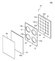
- the 1st Embodiment of this invention is shown,
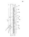
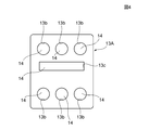
- the exploded perspective view which shows a press detection apparatus and an external appearance formation member, 1 is an exploded perspective view showing the structure of the press detection device shown in FIG. 1 is a longitudinal sectional view of the press detection device shown in FIGS. Front view showing a modified example of the spacer,
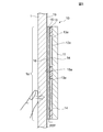
- the 2nd Embodiment of this invention is shown,
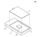
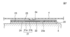
- the exploded perspective view which shows a press detection apparatus and an external appearance formation member Sectional drawing which shows the press detection apparatus shown in FIG.
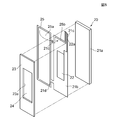
- FIG. 7 is an exploded perspective view showing an example of the structure of the press detection device shown in FIG.
- FIG. 1 shows a first embodiment, and shows an appearance forming member 1 and a pressure detection device 10 installed on a part thereof.
- the appearance forming member 1 forms the appearance of the device, and the appearance forming member 1 in the embodiment shown in FIG. 1 is used for cosmetics or trial wear of clothes having a reflective surface as a whole. It is a home or business mirror. A part of the appearance forming member 1 becomes the operation panel unit 1a, and the press detection device 10 is attached to the back side of the operation panel unit 1a.
- the press detection device 10 has an electrode member 11.
- the electrode member 11 is a hard substrate and a glass epoxy substrate.
- a fixed electrode 12 is provided on the front surface 11 a of the electrode member 11.
- the fixed electrode 12 includes a plurality of X electrodes 12x and a plurality of Y electrodes 12y. Although the X electrode 12x and the Y electrode 12y intersect, the X electrode 12x and the Y electrode 12y are insulated from each other at the intersection. Alternatively, the plurality of X electrodes 12x and the plurality of Y electrodes 12y may be formed on different surfaces of the substrate.
- a spacer 13 is installed on the front surface 11a of the electrode member 11, and a counter member 15 is installed in front of it.
- the spacer 13 is thin such as a resin film, and preferably a double-sided adhesive tape having an adhesive layer formed on both sides of the resin film is used.
- a plurality of circular holes 13 a are formed in the spacer 13, and the inside of the holes 13 a becomes a sensing region 14 of the pressure detection device 10.
- a counter member 15 is provided in front of the spacer 13.
- the counter member 15 is provided with a counter electrode having a wide area that can be opposed to all of the plurality of sensing regions 14.
- the facing member 15 is formed of a flexible member that is lower in rigidity than the electrode member 11 and can be bent and deformed.
- the facing member 15 is formed of a flexible sheet.
- the opposing member 15 is a metal foil such as a copper foil or an aluminum foil. In this case, the entire opposing member 15 serves as an opposing electrode.
- a metal layer such as copper or silver is formed on the surface of the resin sheet by a vapor deposition process or the like, or the metal layer is formed by printing or the like. In this case, the metal layer becomes a counter electrode.
- the electrode member 11 and the counter member 15 are fixed to each other with the spacer 13 interposed therebetween.
- the fixed electrode 12 formed on the electrode member 11 and the counter electrode formed on the counter member 15 face each other in the sensing region 14 inside the hole 13 a of the spacer 13.
- the counter electrode is preferably set to the ground potential.
- a strip is formed on a part of the opposing member 15, the strip is extended to the position of the electrode member 11, and a part of the counter electrode is connected to the ground potential portion of the electrode member 11 by soldering. .
- the pressure detection device 10 is provided with an adhesive layer 16 on the front surface 15a of the facing member 15.
- the adhesive layer 16 may be formed by being transferred to the front surface 15a of the opposing member 15, or may be formed by sticking a double-sided adhesive tape to the front surface 15a of the opposing member 15.
- the pressure-sensitive adhesive layer 16 has viscosity and stacking properties, and fixes the almost entire surface of the facing member 15 to the back surface 1b of the appearance forming member 1 in close contact.
- an adhesive layer that is cured by mixing two liquids or a UV adhesive that is cured by ultraviolet rays may be used instead of the adhesive layer 16.
- the fixed electrode 12 provided on the electrode member 11 is a mutual capacitance detection type electrostatic sensor, and a capacitance is formed between the X electrode 12x and the Y electrode 12y.
- a pulsed voltage is sequentially applied to the plurality of X electrodes 12x, a current flows through the Y electrode 12y when the voltage rises and falls.
- a control unit (not shown) can detect a current value of the Y electrode 12y in order, thereby obtaining a coordinate detection output indicating where a ground potential object is approaching.
- the facing distance between the fixed electrode 12 and the counter electrode is short in the sensing region 14.
- the spacer 13 is formed of a resin film such as PET (polyethylene terephthalate), or a thin double-sided adhesive tape having adhesive layers on both sides of the resin film.
- the thickness of the spacer that is, the facing distance between the front surface 11a of the electrode member 11 and the facing member 15 in the sensing region 14 is preferably 500 ⁇ m or less, more preferably 300 ⁇ m or less, or even more preferably 100 ⁇ m or less.
- the opposing member 15 needs to be lower in rigidity than the electrode member 11 so as to bend together with the appearance forming member 1.
- the thickness dimension of the facing member 15 is preferably, for example, 1 mm or less, and more preferably 500 ⁇ m or less.
- the same electrode can be used even when the shape or position of the sensing region 14 is changed.
- the member 11 can be used as it is.
- FIG. 4 shows a modified spacer 13A.
- the spacer 13A is formed with a plurality of circular holes 13b and slits 13c that extend in a straight line having a length that is larger than the width, and both the inside of the hole 13b and the inside of the slit 13c are both in the sensing region 14. It has become.
- the thickness may be uniform between the operation panel and the surrounding area.
- the thickness dimension may be uniform between the area facing the sensing area 14 and the surrounding area.
- a frame or the like may be displayed on the surface of the housing so that the region of the operation panel unit can be understood, or a display indicating a pressed location may be formed in a portion facing the sensing region 14.
- the region facing the sensing region 14 may be formed slightly thinner than its surroundings.
- FIG. 6 shows a portable information terminal 2 used as a portable phone or the like with the back surface 2a side up.
- An opening 3 is formed in the housing on the back surface 2 a, and the opening 3 is covered with a detachable lid 4.
- the lid 4 is made of a synthetic resin material.
- the lid body 4 is a part of the casing of the portable information terminal 2. In this embodiment, the lid body 4 is an appearance forming member.
- the press detection device 20 is housed inside the opening 3 of the portable information terminal 2. As shown in the cross-sectional view of FIG. 7, the press detection device 20 is installed on the support substrate 4 fixed inside the housing.
- the press detection device 20 includes an electrode member 21 including a hard support plate 21a and a film substrate 21b attached to the front surface thereof.
- a fixed electrode 22 is provided on the front surface of the film substrate 21b.
- the fixed electrode 22 is an X electrode and a Y electrode of the same mutual capacitance detection method as shown in FIGS. Alternatively, as shown in FIG. 5, it is a self-capacitance detection type single electrode.
- a spacer 23 is provided at the front of the film substrate 21b.
- the spacer 23 is an organic insulating layer such as a resist material.
- a hole 23 a is formed in the spacer 23, and the inside thereof is a sensing region 24.
- a counter member 25 is superimposed on the front portion of the spacer 23.
- the counter member 25 has a counter electrode such as a copper foil or a silver pace coating film formed on almost the entire surface of the resin film (the surface facing the fixed electrode 22). Inside the sensing region 24, the fixed electrode 22 and the counter electrode formed on the counter member 25 face each other.
- the pressure detection device 20 is disposed in a thin space on the portable back, the pressure detection device 20 is preferably thin, and the thickness of the spacer 23 is 500 ⁇ m as in the first embodiment. The following is preferable, further 300 ⁇ m or less is preferable, or 100 ⁇ m or less is preferable. Further, the facing member 25 is preferably 500 ⁇ m or less.
- the electrode member 21 has a film substrate 21b supported by a hard support plate 21a, and the film substrate 21b and the opposing member 25 are integrally formed of a film base material such as PET.
- the film substrate 21b and the opposing member 25 are connected by connecting portions 21d and 21d.
- a fixed electrode 22 is formed of copper foil, silver paste, or the like on the front surface of the film substrate 21b.
- a counter electrode 25a is formed on the counter member 25 with copper foil, silver paste, or the like.
- a wiring band 21c extends integrally with the film substrate 21b, and a lead portion 22a extending from the fixed electrode 22 and a lead portion 25b extending from the counter electrode 25a are formed on the wiring band 21c and drawn out.
- the counter electrode 25a is set to the ground potential.
- 2 and 3 can also be formed by folding the film substrate as shown in FIG.
Landscapes
- Engineering & Computer Science (AREA)
- General Engineering & Computer Science (AREA)
- Theoretical Computer Science (AREA)
- Human Computer Interaction (AREA)
- Physics & Mathematics (AREA)
- General Physics & Mathematics (AREA)
- Push-Button Switches (AREA)
Abstract
[Problème] Fournir un dispositif de détection de pression capable de détecter des opérations de pression même sans prévoir un trou ou analogue dans un élément de formation d'aspect, lesdites opérations de pression étant effectuées à partir de l'extérieur de l'élément de formation d'aspect. [Solution] Dans un dispositif de détection de pression 10, un contre-élément 15 chevauche un élément d'électrode 11 avec un espaceur mince 13 entre eux, et une électrode fixe 12x et une contre-électrode sont en face l'une de l'autre dans une région de détection 14, Le contre-élément 15 est lié à la surface arrière d'une section de panneau de commande 1a avec une couche adhésive 16 entre eux, ladite section de panneau de commande étant une partie de l'élément de formation d'aspect 1, L'élément de formation d'aspect 1 est, par exemple, un miroir. Lorsqu'une partie du miroir est pressée, le miroir se déforme, le contre-élément 15 se déforme avec le miroir, une distance entre l'électrode fixe 12x et la contre-électrode raccourcit, et une opération de pression est entrée lorsque le raccourcissement est détectée.
Priority Applications (1)
| Application Number | Priority Date | Filing Date | Title |
|---|---|---|---|
| JP2017523154A JP6495447B2 (ja) | 2015-06-11 | 2016-04-27 | 押圧検知装置 |
Applications Claiming Priority (2)
| Application Number | Priority Date | Filing Date | Title |
|---|---|---|---|
| JP2015-118557 | 2015-06-11 | ||
| JP2015118557 | 2015-06-11 |
Publications (1)
| Publication Number | Publication Date |
|---|---|
| WO2016199517A1 true WO2016199517A1 (fr) | 2016-12-15 |
Family
ID=57504765
Family Applications (1)
| Application Number | Title | Priority Date | Filing Date |
|---|---|---|---|
| PCT/JP2016/063173 Ceased WO2016199517A1 (fr) | 2015-06-11 | 2016-04-27 | Dispositif de détection de pression |
Country Status (2)
| Country | Link |
|---|---|
| JP (1) | JP6495447B2 (fr) |
| WO (1) | WO2016199517A1 (fr) |
Cited By (1)
| Publication number | Priority date | Publication date | Assignee | Title |
|---|---|---|---|---|
| US11099692B2 (en) | 2017-05-22 | 2021-08-24 | Tangi0 Limited | Sensor device and method |
Citations (4)
| Publication number | Priority date | Publication date | Assignee | Title |
|---|---|---|---|---|
| WO2006095684A1 (fr) * | 2005-03-08 | 2006-09-14 | Nissha Printing Co., Ltd. | Unite d’ecran tactile |
| JP2009193859A (ja) * | 2008-02-15 | 2009-08-27 | Mitsumi Electric Co Ltd | ボタンスイッチ |
| JP2012066640A (ja) * | 2010-09-21 | 2012-04-05 | Yupiteru Corp | 車載用電子機器 |
| WO2014113542A1 (fr) * | 2013-01-17 | 2014-07-24 | Microchip Technology Incorporated | Capteurs tactiles capacitifs de force physique |
Family Cites Families (2)
| Publication number | Priority date | Publication date | Assignee | Title |
|---|---|---|---|---|
| TWI271645B (en) * | 2005-04-19 | 2007-01-21 | Elan Microelectronics Corp | Capacitive touchpad with a physical key function |
| JP5003385B2 (ja) * | 2006-10-31 | 2012-08-15 | アイシン精機株式会社 | 車両のシート用乗員荷重検出装置 |
-
2016
- 2016-04-27 WO PCT/JP2016/063173 patent/WO2016199517A1/fr not_active Ceased
- 2016-04-27 JP JP2017523154A patent/JP6495447B2/ja active Active
Patent Citations (4)
| Publication number | Priority date | Publication date | Assignee | Title |
|---|---|---|---|---|
| WO2006095684A1 (fr) * | 2005-03-08 | 2006-09-14 | Nissha Printing Co., Ltd. | Unite d’ecran tactile |
| JP2009193859A (ja) * | 2008-02-15 | 2009-08-27 | Mitsumi Electric Co Ltd | ボタンスイッチ |
| JP2012066640A (ja) * | 2010-09-21 | 2012-04-05 | Yupiteru Corp | 車載用電子機器 |
| WO2014113542A1 (fr) * | 2013-01-17 | 2014-07-24 | Microchip Technology Incorporated | Capteurs tactiles capacitifs de force physique |
Cited By (3)
| Publication number | Priority date | Publication date | Assignee | Title |
|---|---|---|---|---|
| US11099692B2 (en) | 2017-05-22 | 2021-08-24 | Tangi0 Limited | Sensor device and method |
| GB2564929B (en) * | 2017-05-22 | 2022-10-05 | Tangi0 Ltd | Sensor device and method |
| EP3631609B1 (fr) * | 2017-05-22 | 2023-12-06 | Tangi0 Limited | Dispositif de capteur capacitif |
Also Published As
| Publication number | Publication date |
|---|---|
| JP6495447B2 (ja) | 2019-04-03 |
| JPWO2016199517A1 (ja) | 2018-03-01 |
Similar Documents
| Publication | Publication Date | Title |
|---|---|---|
| JP5347913B2 (ja) | センサ装置、電子機器、及びセンサ装置の製造方法 | |
| CN102483363B (zh) | 压力检测单元以及压力检测装置 | |
| JP5540797B2 (ja) | センサ装置および表示装置 | |
| US8395587B2 (en) | Haptic response apparatus for an electronic device | |
| WO2011125389A1 (fr) | Feuille piézoélectrique transparente avec armature contenant la feuille piézoélectrique transparente, panneau tactile contenant la feuille piézoélectrique transparente, et dispositif électronique | |
| TWI625653B (zh) | Sensing device, input device and electronic device | |
| US20190094007A1 (en) | Curvature radius measurer, electronic device and method of manufacturing curvature radius measurer | |
| JP2013008231A (ja) | 静電容量方式にも抵抗膜方式にも対応可能な押圧検出機能を有するタッチパネル | |
| JP2016149352A (ja) | 静電容量型入力装置 | |
| JP2009026151A (ja) | 入力装置及び電子機器 | |
| CN107678217B (zh) | 一种液晶显示面板及液晶显示装置 | |
| JP6495447B2 (ja) | 押圧検知装置 | |
| CN107122073B (zh) | 显示装置 | |
| US8857276B2 (en) | Pressure detection unit | |
| CN105320348B (zh) | 触摸面板与前表面设计板的固定构造 | |
| TW201535195A (zh) | 具有三維形狀的觸控面板、觸控面板的驅動方法和觸控面板的校準方法 | |
| JP6147469B2 (ja) | タッチセンサ | |
| CN107193408A (zh) | 电子装置 | |
| JP6706760B2 (ja) | タッチセンサおよび電子機器 | |
| KR20190102114A (ko) | 표시 장치 | |
| CN108108071B (zh) | 触控面板及其制备方法、触控显示屏及其制备方法 | |
| JP7109325B2 (ja) | 操作装置 | |
| KR102930138B1 (ko) | 전자 기기 | |
| JP2008071239A (ja) | 入力装置 | |
| JP7223957B2 (ja) | タッチセンサ |
Legal Events
| Date | Code | Title | Description |
|---|---|---|---|
| 121 | Ep: the epo has been informed by wipo that ep was designated in this application |
Ref document number: 16807224 Country of ref document: EP Kind code of ref document: A1 |
|
| ENP | Entry into the national phase |
Ref document number: 2017523154 Country of ref document: JP Kind code of ref document: A |
|
| NENP | Non-entry into the national phase |
Ref country code: DE |
|
| 122 | Ep: pct application non-entry in european phase |
Ref document number: 16807224 Country of ref document: EP Kind code of ref document: A1 |