WO2016199632A1 - Élément de conversion photoélectrique, procédé de fabrication d'élément de conversion photoélectrique, et dispositif d'imagerie à semi-conducteur - Google Patents
Élément de conversion photoélectrique, procédé de fabrication d'élément de conversion photoélectrique, et dispositif d'imagerie à semi-conducteur Download PDFInfo
- Publication number
- WO2016199632A1 WO2016199632A1 PCT/JP2016/066147 JP2016066147W WO2016199632A1 WO 2016199632 A1 WO2016199632 A1 WO 2016199632A1 JP 2016066147 W JP2016066147 W JP 2016066147W WO 2016199632 A1 WO2016199632 A1 WO 2016199632A1
- Authority
- WO
- WIPO (PCT)
- Prior art keywords
- group
- photoelectric conversion
- groups
- conversion element
- electrode
- Prior art date
- Legal status (The legal status is an assumption and is not a legal conclusion. Google has not performed a legal analysis and makes no representation as to the accuracy of the status listed.)
- Ceased
Links
Images




Classifications
-
- H—ELECTRICITY
- H10—SEMICONDUCTOR DEVICES; ELECTRIC SOLID-STATE DEVICES NOT OTHERWISE PROVIDED FOR
- H10K—ORGANIC ELECTRIC SOLID-STATE DEVICES
- H10K39/00—Integrated devices, or assemblies of multiple devices, comprising at least one organic radiation-sensitive element covered by group H10K30/00
- H10K39/30—Devices controlled by radiation
- H10K39/32—Organic image sensors
-
- H—ELECTRICITY
- H10—SEMICONDUCTOR DEVICES; ELECTRIC SOLID-STATE DEVICES NOT OTHERWISE PROVIDED FOR
- H10K—ORGANIC ELECTRIC SOLID-STATE DEVICES
- H10K30/00—Organic devices sensitive to infrared radiation, light, electromagnetic radiation of shorter wavelength or corpuscular radiation
- H10K30/30—Organic devices sensitive to infrared radiation, light, electromagnetic radiation of shorter wavelength or corpuscular radiation comprising bulk heterojunctions, e.g. interpenetrating networks of donor and acceptor material domains
-
- H—ELECTRICITY
- H10—SEMICONDUCTOR DEVICES; ELECTRIC SOLID-STATE DEVICES NOT OTHERWISE PROVIDED FOR
- H10K—ORGANIC ELECTRIC SOLID-STATE DEVICES
- H10K30/00—Organic devices sensitive to infrared radiation, light, electromagnetic radiation of shorter wavelength or corpuscular radiation
- H10K30/80—Constructional details
- H10K30/81—Electrodes
- H10K30/82—Transparent electrodes, e.g. indium tin oxide [ITO] electrodes
-
- H—ELECTRICITY
- H10—SEMICONDUCTOR DEVICES; ELECTRIC SOLID-STATE DEVICES NOT OTHERWISE PROVIDED FOR
- H10K—ORGANIC ELECTRIC SOLID-STATE DEVICES
- H10K85/00—Organic materials used in the body or electrodes of devices covered by this subclass
- H10K85/30—Coordination compounds
- H10K85/321—Metal complexes comprising a group IIIA element, e.g. Tris (8-hydroxyquinoline) gallium [Gaq3]
- H10K85/322—Metal complexes comprising a group IIIA element, e.g. Tris (8-hydroxyquinoline) gallium [Gaq3] comprising boron
-
- H—ELECTRICITY
- H10—SEMICONDUCTOR DEVICES; ELECTRIC SOLID-STATE DEVICES NOT OTHERWISE PROVIDED FOR
- H10F—INORGANIC SEMICONDUCTOR DEVICES SENSITIVE TO INFRARED RADIATION, LIGHT, ELECTROMAGNETIC RADIATION OF SHORTER WAVELENGTH OR CORPUSCULAR RADIATION
- H10F39/00—Integrated devices, or assemblies of multiple devices, comprising at least one element covered by group H10F30/00, e.g. radiation detectors comprising photodiode arrays
- H10F39/10—Integrated devices
- H10F39/12—Image sensors
- H10F39/191—Photoconductor image sensors
-
- H—ELECTRICITY
- H10—SEMICONDUCTOR DEVICES; ELECTRIC SOLID-STATE DEVICES NOT OTHERWISE PROVIDED FOR
- H10K—ORGANIC ELECTRIC SOLID-STATE DEVICES
- H10K30/00—Organic devices sensitive to infrared radiation, light, electromagnetic radiation of shorter wavelength or corpuscular radiation
- H10K30/50—Photovoltaic [PV] devices
-
- Y—GENERAL TAGGING OF NEW TECHNOLOGICAL DEVELOPMENTS; GENERAL TAGGING OF CROSS-SECTIONAL TECHNOLOGIES SPANNING OVER SEVERAL SECTIONS OF THE IPC; TECHNICAL SUBJECTS COVERED BY FORMER USPC CROSS-REFERENCE ART COLLECTIONS [XRACs] AND DIGESTS
- Y02—TECHNOLOGIES OR APPLICATIONS FOR MITIGATION OR ADAPTATION AGAINST CLIMATE CHANGE
- Y02E—REDUCTION OF GREENHOUSE GAS [GHG] EMISSIONS, RELATED TO ENERGY GENERATION, TRANSMISSION OR DISTRIBUTION
- Y02E10/00—Energy generation through renewable energy sources
- Y02E10/50—Photovoltaic [PV] energy
- Y02E10/549—Organic PV cells
-
- Y—GENERAL TAGGING OF NEW TECHNOLOGICAL DEVELOPMENTS; GENERAL TAGGING OF CROSS-SECTIONAL TECHNOLOGIES SPANNING OVER SEVERAL SECTIONS OF THE IPC; TECHNICAL SUBJECTS COVERED BY FORMER USPC CROSS-REFERENCE ART COLLECTIONS [XRACs] AND DIGESTS
- Y02—TECHNOLOGIES OR APPLICATIONS FOR MITIGATION OR ADAPTATION AGAINST CLIMATE CHANGE
- Y02P—CLIMATE CHANGE MITIGATION TECHNOLOGIES IN THE PRODUCTION OR PROCESSING OF GOODS
- Y02P70/00—Climate change mitigation technologies in the production process for final industrial or consumer products
- Y02P70/50—Manufacturing or production processes characterised by the final manufactured product
Definitions
- the present disclosure relates to a photoelectric conversion element used for, for example, a CCD (Charge Coupled Device) or a CMOS (Complementary Metal Oxide Semiconductor) image sensor, a method for manufacturing the photoelectric conversion element, and a solid-state imaging device.
- a photoelectric conversion element used for, for example, a CCD (Charge Coupled Device) or a CMOS (Complementary Metal Oxide Semiconductor) image sensor, a method for manufacturing the photoelectric conversion element, and a solid-state imaging device.
- CCD Charge Coupled Device
- CMOS Complementary Metal Oxide Semiconductor
- a lower electrode, a photoelectric conversion layer made of an organic semiconductor, and an upper electrode are stacked in this order on a substrate.
- Various intermediate layers such as an electron block layer, a buffer layer, and an active layer may be provided between the photoelectric conversion layer and each electrode.
- the photoresponsiveness in the photoelectric conversion layer is important.
- a solid-state imaging device used in a digital camera or the like if this light response is low, an afterimage is generated when a moving subject is imaged or a moving image is captured. For this reason, improvement of photoresponsiveness is desired.
- Patent Documents 4 and 5 propose specific methods for improving responsiveness in a solid-state imaging device using an organic semiconductor as a photoelectric conversion layer.
- the photoelectric conversion layer is formed of at least one organic compound semiconductor
- the hole mobility of the photoelectric conversion layer is h1
- the electron mobility is e1
- An element structure that satisfies e1 ⁇ 10 has been proposed.
- the hole mobility of the photoelectric conversion layer is h1, and the electron mobility is e1, 0.1 ⁇ h1 / While satisfying e1 ⁇ 10, the hole mobility h1 is 8.5E-6 cm 2 / Vs or more and 3.8E-5 cm 2 / Vs or less, and the electron mobility e1 is 9.3E-7 cm 2 / Vs.
- a method of controlling to 7.6E-5 cm 2 / Vs or less has been proposed. Realization of a simpler method different from these methods is desired.
- a photoelectric conversion element is provided on a first electrode, a first electrode, a photoelectric conversion layer including an organic semiconductor having a quantum efficiency of 1% or less, and a photoelectric conversion layer.
- the second electrode is provided.
- a photoelectric conversion layer including an organic semiconductor having a quantum efficiency of 1% or less is formed on a first electrode, and the second electrode is formed on the photoelectric conversion layer. Is formed.
- a solid-state imaging device includes the photoelectric conversion element according to the embodiment of the present disclosure.
- the quantum efficiency of the organic semiconductor included in the photoelectric conversion layer is 1% or less.
- the quantum efficiency (of the organic semiconductor alone) of a single layer film composed of one organic semiconductor is high, the energy level of the single layer film is likely to expand. That is, HOMO (Highest Occupied Molecular Orbital) levels or LUMO (Lowest Unoccupied Molecular Orbital) levels are randomly distributed, and exciton dissociation is easily promoted by light absorption.
- the photoelectric conversion layer includes an organic semiconductor having a quantum efficiency of 1% or less. , The spread of energy levels can be suppressed and free carriers can be easily conducted. Therefore, it is possible to improve photoresponsiveness.
- FIG. 4 is a cross-sectional view for explaining a step following the step in FIG. 3.
- FIG. 5 is a cross-sectional view for explaining a step following the step in FIG. 4.
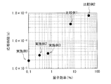
- FIG. 6 is a characteristic diagram showing a relationship between quantum efficiency and response time in Examples 1 to 3. It is a functional block diagram showing an example of an application example (camera).
- Embodiment an example of a photoelectric conversion element having a photoelectric conversion layer including an organic semiconductor having a quantum efficiency of 1% or less and a solid-state imaging element
- Example Example using a subphthalocyanine derivative in the photoelectric conversion layer
- Application example (camera example)
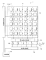
- FIG. 1A illustrates a functional configuration of a solid-state imaging device (solid-state imaging device 1) according to an embodiment of the present disclosure.
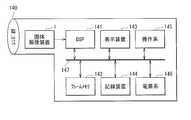
- FIG. 1B illustrates a configuration of an electronic device in which the solid-state imaging device 1 is mounted.
- the solid-state imaging device 1 is, for example, a CCD or a CMOS image sensor.
- 1B for example, the lens group 140, the solid-state imaging device 1, the digital signal processor (DSP) 141, the frame memory 142, the display device 143, the recording device 144, the operation system 145, and the power supply system 146. It is comprised including.
- the DSP 141, the frame memory 142, the display device 143, the recording device 144, the operation system 145, and the power supply system 146 are electrically connected by a bus line 147.
- the solid-state imaging device 1 includes, for example, an imaging region 1a, a vertical drive circuit 131, a column signal processing circuit 133, a horizontal drive circuit 134, an output circuit 136, and a control circuit 130 on a semiconductor substrate (for example, a silicon semiconductor substrate). And have. In the imaging area 1a, a plurality of pixels P including a photoelectric conversion element 10 described later are arranged in a two-dimensional array. Note that circuits such as the vertical drive circuit 131, the column signal processing circuit 133, the horizontal drive circuit 134, the output circuit 136, and the control circuit 130 can be configured from various circuits used in the solid-state imaging device.
- the solid-state imaging device 1 may be a so-called front side irradiation type or a so-called back side irradiation type.
- a shutter device for controlling the incidence of light on the pixel P may be arranged as necessary.
- the vertical drive circuit 131 is constituted by a shift register, for example, and selectively scans each pixel P in the imaging region 1a in the vertical direction sequentially in units of rows.
- a pixel signal (a signal based on a current generated according to the amount of received light) output from each pixel P in the pixel row selectively scanned by the vertical drive circuit 131 is sent to the column signal processing circuit 133 via the vertical signal line 132. It is done.
- the column signal processing circuit 133 is arranged for each pixel column, for example, and is formed for each pixel P in a black reference pixel (for example, a peripheral region of the imaging region 1a) with respect to a signal output from one row of pixels P. For example, signal processing such as noise removal and signal amplification is performed.
- a horizontal selection switch is provided at the output stage of the column signal processing circuit 133, and the column signal processing circuit 133 and the horizontal signal line 135 are connected via the horizontal selection switch.
- the horizontal driving circuit 134 is configured by, for example, a shift register, and sequentially outputs each of the column signal processing circuits 133 by sequentially outputting horizontal scanning pulses, and signals from each of the column signal processing circuits 133 are transmitted to the horizontal signal line 135. Output.
- the output circuit 136 performs signal processing on the signals sequentially supplied from the horizontal signal line 135 and outputs them (generates an output signal Vout).
- the control circuit 130 generates a clock signal and a control signal that serve as a reference for operations of the vertical drive circuit 131, the column signal processing circuit 133, and the horizontal drive circuit 134 based on, for example, a vertical synchronization signal, a horizontal synchronization signal, and a master clock. It is.
- the generated clock signal and control signal are input to the vertical drive circuit 131, the column signal processing circuit 133, and the horizontal drive circuit 134.
- the imaging region 1a has, for example, a plurality of pixels P that are two-dimensionally arranged in a matrix.
- a pixel drive line Lread (specifically, a row selection line and a reset control line) is arranged for each pixel row, and a vertical signal line 132 is arranged for each pixel column.
- the pixel drive line Lread supplies a drive signal for reading a signal from the pixel.
- One end of the pixel drive line Lread is connected to an output end corresponding to each row of the vertical drive circuit 131.
- Each pixel P is formed with a photoelectric conversion element using an organic semiconductor, as will be described in detail later.
- An on-chip lens and a protective film may be provided on the light incident side of the imaging region 1a.
- the color filter may or may not be provided as necessary.
- the photoelectric conversion layer itself can function as a color filter by selecting a photoelectric conversion material. In such a case, color separation is possible without providing a color filter.
- a color filter is disposed on the light incident side of the pixel P, for example, a known color filter that transmits one or more wavelengths of red, green, blue, cyan, magenta, yellow, and the like is used. be able to.
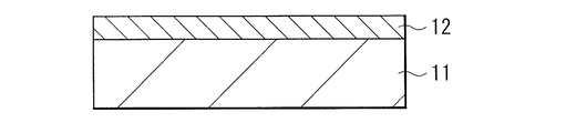
- FIG. 2 schematically shows a main configuration of a photoelectric conversion element (photoelectric conversion element 10) formed in each pixel of the imaging region 1a.
- the photoelectric conversion element 10 includes a first electrode (pixel electrode) 12, a photoelectric conversion layer 13, and a second electrode 14 in this order on a support substrate 11.
- the photoelectric conversion element 10 is configured such that light can be incident from both the first electrode 12 side and the second electrode 14 side (upper and lower) of the photoelectric conversion layer 13.
- the incident direction of light is not particularly limited, and may be configured such that light can be incident only from the first electrode 12 side, or configured such that light can be incident only from the second electrode 14 side. It doesn't matter.
- the support substrate 11 is made of a material such as glass, plastic or silicon.
- the substrate material is not particularly limited, but when light is incident from the first electrode 12 side, a material having transparency in the visible light region is selected.
- the support substrate 11 is formed of a silicon semiconductor substrate, the above-described drive circuit is provided on the silicon semiconductor substrate, and the photoelectric conversion element 10 is mounted on the silicon semiconductor substrate.
- a laminated structure can also be used.
- the first electrode 12 is made of a conductive material such as a transparent conductive film and metal.
- a transparent conductive film having transparency in the visible light region is selected as the constituent material of the first electrode 12.
- the transparent conductive film include indium tin oxide (ITO), indium gallium zinc (IGZO), zinc oxide (ZnO), indium zinc oxide (IZO), iridium dioxide (IrO 2 ), and titanium dioxide (TiO 2 ).
- a transparent conductive film comprising at least one of tin dioxide (SnO 2 ).
- An example of the metal material is aluminum (Al).
- the photoelectric conversion layer 13 includes at least one organic semiconductor. Desirably, it includes different types of materials, specifically, a hole transporting material (donor material) and an electron transporting material (acceptor material). This is because a bulk heterojunction (bulk heterostructure) is formed by mixing the hole transporting material and the electron transporting material, and the photoelectric conversion efficiency can be increased.
- the hole transporting material and the electron transporting material are formed, for example, by being stacked or mixed in the photoelectric conversion layer 13.
- the organic semiconductor various organic pigments can be used.
- subphthalocyanine derivatives for example, subphthalocyanine derivatives, quinacridone derivatives, phthalocyanine derivatives, oxadiazole derivatives, stilbene derivatives, perylene derivatives, tetracyanoquinodimethane derivatives, phenanthroline derivatives. , Naphthalene derivatives, pyrene derivatives, and fluoranthene derivatives.
- a metal complex dye etc. may be used.
- other organic materials such as fullerene (C60) and BCP (Bathocuproine) may be laminated on the photoelectric conversion layer 13.
- the film thickness of this photoelectric converting layer 13 is not specifically limited, For example, they are 50 nm or more and 1 micrometer or less.
- the electron transporting material includes a subphthalocyanine derivative among the materials described above.
- the hole transporting material at this time includes, for example, a quinacridone derivative such as 2,9-di-tert-butylquinacridone or N-methylquinacridone.
- the quantum efficiency of at least one organic semiconductor is 1% or less. More desirably, it is 0.1% or more and 0.7% or less.
- the quantum efficiency here is the quantum efficiency of the organic semiconductor itself (of the organic semiconductor alone) and is the quantum efficiency obtained in the single-layer film of the organic semiconductor.
- R1 to R12 are each, for example, a hydrogen atom (H), a halogen atom (F, Cl, Br, I), a linear, branched or cyclic alkyl group, a phenyl group, a linear or condensed aromatic ring Group, partial fluoroalkyl group, perfluoroalkyl group, halide group, silylalkyl group, silylalkoxy group, arylsilyl group, thioalkyl group, thioaryl group, arylsulfonyl group, alkylsulfonyl group, amino group, alkylamino group, Arylamino group, hydroxy group, alkoxy group, acylamino group, acyloxy group, carboxy group, carboximide group, carboalkoxy group, acyl group, sulfonyl group
- M contains boron (B), a divalent metal, or a trivalent metal.
- X includes an anionic group and any one of the same group of substituents as R1 to R12.
- Z represents nitrogen (N), CH, or hydrogen in CH substituted by any one of the same group of substituents as R1 to R12.
- a subphthalocyanine derivative represented by the following general formulas of Chemical Formula 2, Chemical Formula 3, and Chemical Formula 4 is used. That is, in the general formula of the above chemical formula 1, R1, R4, R5, R8, R9, and R12 are hydrogen atoms, and R2, R3, R6, R7, R10, and R11 are fluorine atoms. Further, in Chemical Formula 2, M is boron, X is fluorine, and Z is nitrogen. In Chemical Formula 3, M is boron, X is phenol substituted with fluorine, and Z is nitrogen. In Chemical Formula 4, M is boron, X is chlorine, and Z is nitrogen.
- the single quantum efficiency of each is low (1% or less), and as described in detail later, free carriers after dissociation of excitons are reduced. It becomes easy to conduct, and as a result, photoresponsiveness can be improved. This is due to the following reason. That is, it is considered that by making R2, R3, R6, R7, R10, and R11 in Chemical Formula 1 a fluorine atom, the intermolecular interaction is weakened, thereby increasing the amorphous nature. In the case of an organic semiconductor having an amorphous property, the energy level is less likely to be confused as compared to those containing many grain boundaries such as polycrystal or microcrystal.
- R1 to R12 in Chemical Formula 1 may be a part of a condensed aliphatic ring or a condensed aromatic ring, and these rings contain one or more atoms other than carbon. Also good. Furthermore, as represented by the general formula of Chemical Formula 5 below, it may contain two or more subphthalocyanine derivatives, or has a structure in which one subphthalocyanine derivative and a subporphyrin ring are bonded. You may do it. R13 is a substituent which can be bonded to one or more subphthalocyanine derivatives or subporphyrin rings via M or any part of R1 to R12 (substituents similar to R1 to R12 above). Any of the group of groups).
- the second electrode 14 is made of a conductive material such as a transparent conductive film and metal.
- a transparent conductive film having transparency in the visible light region is selected as the constituent material of the second electrode 14.
- the transparent conductive film include indium tin oxide (ITO), indium gallium zinc (IGZO), zinc oxide (ZnO), indium zinc oxide (IZO), iridium dioxide (IrO 2 ), and titanium dioxide (TiO 2 ).
- a transparent conductive film comprising at least one of tin dioxide (SnO 2 ).
- An example of the metal material is aluminum (Al).
- FIG. 3 are schematic views for explaining a manufacturing method of the photoelectric conversion element 10 shown in FIG.
- the photoelectric conversion element 10 can be manufactured as follows, for example. That is, first, as shown in FIG. 3, the first electrode 12 made of the above-described material (for example, ITO) is formed on the support substrate 11 made of the above-described material by a sputtering method, for example, with a film thickness of about 100 nm. To do. Thereafter, the first electrode 12 is patterned by etching using, for example, a photolithography method.
- the first electrode 12 made of the above-described material for example, ITO
- a sputtering method for example, with a film thickness of about 100 nm.
- the first electrode 12 is patterned by etching using, for example, a photolithography method.
- the photoelectric conversion layer 13 is formed on the first electrode 12.
- a mixture of a hole transporting material and an electron transporting material as described above, for example, by vapor deposition using a resistance heating type vacuum vapor deposition apparatus is formed on the first electrode 12 with, for example, 100 nm.
- the film is formed with a film thickness.
- the photoelectric conversion layer 13 can be formed by various methods in addition to the resistance heating type vacuum deposition method as described above, depending on the material to be used. Examples thereof include various chemical vapor deposition methods (CVD methods) including coating methods, physical vapor deposition methods (PVD methods), and MOCVD methods. Examples of coating methods include spin coating, dipping, casting, screen printing, inkjet printing, offset printing, gravure printing, stamping, spraying, air doctor coater, blade coater, and rod coater. Method, knife coater method, squeeze coater method, reverse roll coater method, transfer roll coater method, gravure coater method, kiss coater method, cast coater method, spray coater method, slit orifice coater method and calendar coater method.
- CVD methods chemical vapor deposition methods
- PVD methods physical vapor deposition methods
- MOCVD methods MOCVD methods
- coating methods include spin coating, dipping, casting, screen printing, inkjet printing, offset printing, gravure printing, stamping, spraying, air doctor coater, blade coater
- a nonpolar or low polarity organic solvent such as toluene, chloroform, hexane, or ethanol can be used as the solvent.
- a vacuum deposition method electron beam heating method, resistance heating method, flash deposition, etc.
- plasma deposition method sputtering method (bipolar sputtering method, direct current sputtering method, direct current magnetron sputtering method, high frequency sputtering method, magnetron) Sputtering method, ion beam sputtering method, bias sputtering method, etc.), ion plating method (DC (direct current) method, RF method, multi-cathode method, activation reaction method, field evaporation method, high-frequency ion plating method, reactivity) Ion plating method).
- DC direct current
- the second electrode 14 made of the above-described material (for example, Al) is formed on the photoelectric conversion layer 13 with a film thickness of 100 nm by, for example, a vacuum deposition method.
- the photoelectric conversion element 10 which has the photoelectric converting layer 13 which has a bulk heterojunction shown in FIG. 2 can be manufactured.
- the solid-state imaging device 1 of the present embodiment light incident on the imaging region 1a is photoelectrically converted in the photoelectric conversion element 10 of each pixel P. Specifically, the light incident on the photoelectric conversion element 10 passes through the first electrode 12 (or passes through the second electrode 14), for example, and reaches the photoelectric conversion layer 13. In the photoelectric conversion layer 13, pairs of electrons and holes (excitons) are generated, and one of them (for example, electrons) is read to the vertical signal line 132 as a signal charge. The read signal is output to the outside through the horizontal signal line 135. Alternatively, it may be input to the DSP 141 or the like shown in FIG. 1B and held in the recording device 144. In this way, the solid-state imaging device 1 can acquire an electrical signal by photoelectric conversion.
- the photoelectric conversion layer 13 using the organic semiconductor as described above it is desired to improve its photoresponsiveness.
- the organic semiconductor thin film when the quantum efficiency of the organic semiconductor alone is high, the energy level tends to expand in the film. That is, HOMO (Highest Occupied Molecular Orbital) levels or LUMO (Lowest Unoccupied Molecular Orbital) levels are randomly distributed, and exciton dissociation is easily promoted by light absorption.
- the organic semiconductor material itself contained in the photoelectric conversion layer 13 has a low quantum efficiency, specifically, 1% or less, and this makes it difficult to randomly distribute energy levels. Can do. That is, the randomness of the energy level of the organic semiconductor contained in the photoelectric conversion layer affects the quantum efficiency, and in an organic semiconductor having a low quantum efficiency (quantum efficiency of 1% or less), free carriers are easily conducted. This leads to an improvement in photoresponsiveness.
- the photoelectric conversion layer 13 has an electron transporting material and a hole transporting material, and by making the quantum efficiency of the electron transporting material of these materials 1% or less, the photoresponsiveness is effectively improved. Can be made. This is due to the following reason. That is, the photoresponsiveness in the photoelectric conversion element that is generated by pairs of holes and electrons is affected by a carrier type having a low carrier mobility among holes and electrons. Therefore, the responsiveness of the photoelectric conversion element is determined not by the balance between the hole mobility and the electron mobility but by the carrier type having the lower responsiveness. For example, when the photoresponsiveness is easily affected by electron mobility, it is desirable to lower the quantum efficiency of the electron transporting material.
- the quantum efficiency (hereinafter referred to as sensitivity) of the entire photoelectric conversion layer 13 is also an important factor.
- sensitivity the quantum efficiency of the entire photoelectric conversion layer 13
- the photoresponsiveness can be improved as described above, but on the other hand, the organic semiconductor having a low quantum efficiency.
- the sensitivity is lowered.
- the photoelectric conversion layer 13 has a bulk heterojunction made of different materials. Thereby, it is possible to increase the sensitivity of the entire photoelectric conversion layer 13 or to suppress the decrease in sensitivity. This is due to the following reason. That is, in general, in the photoelectric conversion layer 13, excitons generated after light absorption are strongly bound, and free carriers are hardly generated with energy of about room temperature. For this reason, dissociation of excitons can be promoted at the heterointerface by bonding (bulk heterojunction) dissimilar materials (hole transport material and electron transport material) having different energy levels. The energy difference between the molecules constituting the photoelectric conversion layer 13 leads to the promotion of free carrier generation.
- the photoelectric conversion layer 13 includes a bulk heterojunction of an electron transporting material and a hole transporting material, the photoresponsiveness can be improved while increasing the quantum efficiency (sensitivity) of the entire photoelectric conversion layer 13. It is possible to improve two characteristics that are originally in a trade-off relationship.
- the quantum efficiency of the organic semiconductor included in the photoelectric conversion layer 13 is 1% or less, the spread of energy level distribution in the organic semiconductor is suppressed, and free carriers are conducted. It can be made easy. Therefore, it is possible to improve photoresponsiveness.
- Example 1 In the photoelectric conversion element 10 shown in FIG. 2, the response time when the subphthalocyanine derivative shown in Chemical Formula 2 was used as the photoelectric conversion layer 13 was measured.
- a first electrode made of ITO, a photoelectric conversion layer 13, and a second electrode 14 made of Al were formed in this order on a support substrate 11 made of quartz.
- a subphthalocyanine derivative (Chemical Formula 2) was formed to a thickness of 100 nm by a vacuum deposition method.
- the quantum efficiency (%) of the subphthalocyanine derivative (Chemical Formula 2) is ⁇ 5.0 ⁇ 10 5 (V / cm) ( ⁇ 5.0 ⁇ E + 5 (V / cm)) applied to the first electrode 12.
- the light amount when the photocurrent density was 1 ( ⁇ A / cm 2 ) was calculated.
- the response time (s) is excited so that the photocurrent density becomes 1 ( ⁇ A / cm 2 ) when ⁇ 5.0 ⁇ 10 5 (V / cm) is applied to the first electrode 12.
- Light irradiation at a wavelength of 530 nm the time from the end of light irradiation until the photocurrent density attenuates to 0.1 ( ⁇ A / cm 2 ) (that is, the time until the photocurrent attenuates to 10% at the time of light irradiation Time).
- the quantum efficiency of the subphthalocyanine derivative was 0.1%, and the response time was 1.9 ⁇ 10 ⁇ 5 (s).
- Example 1 a device using a subphthalocyanine derivative represented by the following general formula 6 was produced. Furthermore, as a comparative example (comparative example 2) of Example 1, a device using a subphthalocyanine derivative represented by the general formula of Chemical Formula 7 below was produced. In these Comparative Examples 1 and 2 as well, except that the organic semiconductor used for the photoelectric conversion layer was different, an element was produced in the same manner as in Example 1 above, and the quantum efficiency and response time were measured.
- Example 2 In the photoelectric conversion element 10 illustrated in FIG. 2, the response time when the subphthalocyanine derivative represented by Chemical Formula 3 was used as the photoelectric conversion layer 13 was measured. Except that the organic semiconductor used for the photoelectric conversion layer 13 is different, an element was produced in the same manner as in Example 1, and the quantum efficiency and response time were measured.
- the quantum efficiency of the subphthalocyanine derivative was 0.3%, and the response time was 3.0 ⁇ 10 ⁇ 5 (s). Also in Example 2, the response time could be shortened compared to Comparative Examples 1 and 2 above.
- Example 3 In the photoelectric conversion element 10 shown in FIG. 2, the response time when the subphthalocyanine derivative shown in Chemical Formula 4 was used as the photoelectric conversion layer 13 was measured. Except that the organic semiconductor used for the photoelectric conversion layer 13 is different, an element was produced in the same manner as in Example 1, and the quantum efficiency and response time were measured.
- the quantum efficiency of the subphthalocyanine derivative was 0.7%, and the response time was 3.5 ⁇ 10 ⁇ 5 (s). Also in Example 3, the response time could be shortened compared to Comparative Examples 1 and 2 above.
- FIG. 6 shows the response times of Examples 1 to 3 and Comparative Examples 1 and 2.
- Examples 1 to 3 using an organic semiconductor having a quantum efficiency of 1% or less for the photoelectric conversion layer 13 the response time is shorter than those in Comparative Examples 1 and 2 using an organic semiconductor having a quantum efficiency of more than 1%. Recognize.
- the quantum efficiency is 1% or less, which is advantageous for improving the photoresponsiveness.
- Example 4 In the photoelectric conversion element 10 shown in FIG. 2, as the photoelectric conversion layer 13, a bulk heterojunction is formed by mixing an electron transporting material and a hole transporting material. The response time was measured when subphthalocyanine derivatives were used.
- a first electrode made of ITO, a photoelectric conversion layer 13, and a second electrode 14 made of Al were formed in this order on a support substrate 11 made of quartz.
- a subphthalocyanine derivative (Chemical Formula 2) and 2,9-di-tert-butylquinacridon as a hole transporting material are deposited at a deposition rate of 1: 1 to 100 nm by vacuum deposition.
- the response time (s) was measured in the same manner as in Example 1.
- the quantum efficiency of the subphthalocyanine derivative (Chemical Formula 2) is 0.1% as described in Example 1.
- Example 4 Comparative Example 3
- an element using a subphthalocyanine derivative represented by the general formula of Chemical Formula 6 as an electron transporting material was prepared, and other conditions were the same as in Example 4. The response time was measured.
- Example 4 As a result of the above measurement, in Example 4 using the photoelectric conversion layer 13 in which a bulk heterojunction was formed using a subphthalocyanine derivative (chemical formula 2) having a quantum efficiency of 0.1%, the response time was 4.0 ⁇ 10 ⁇ . 5 (s). In Comparative Example 3, it was 3.5 ⁇ 10 ⁇ 4 (s). In Example 4, compared with Comparative Example 3, the response time could be shortened.
- a subphthalocyanine derivative chemical formula 2 having a quantum efficiency of 0.1%
- Example 5 In the photoelectric conversion element 10 illustrated in FIG. 2, as the photoelectric conversion layer 13, an electron transporting material and a hole transporting material are stacked to form a bulk heterojunction. The response time when a subphthalocyanine derivative was used was measured.
- a first electrode made of ITO, a photoelectric conversion layer 13, and a second electrode 14 made of Al were formed in this order on a support substrate 11 made of quartz.
- the first electrode 12 was formed with a thickness of 100 nm by sputtering.
- a subphthalocyanine derivative (Chemical Formula 3) and N-methylquinacridone as a hole transporting material were formed to a thickness of 100 nm by a vacuum deposition method at a deposition rate of 1: 1.
- the response time (s) was measured in the same manner as in Example 1. Further, as described in Example 2, the quantum efficiency of the subphthalocyanine derivative (Chemical Formula 3) is 0.3%.
- Example 5 Comparative Example 4
- an element using a subphthalocyanine derivative represented by the general formula of Chemical Formula 6 as an electron transporting material was prepared, and other conditions were the same as in Example 5. The response time was measured.
- Example 5 As a result of the above measurement, in Example 5 using the photoelectric conversion layer 13 in which a bulk heterojunction was formed using a subphthalocyanine derivative (chemical formula 3) having a quantum efficiency of 0.3%, the response time was 2.0 ⁇ 10 ⁇ . 5 (s). In Comparative Example 4, it was 3.0 ⁇ 10 ⁇ 4 (s). In Example 5, compared with Comparative Example 3, the response time could be shortened.
- a subphthalocyanine derivative chemical formula 3
- Example 6 In the photoelectric conversion element 10 illustrated in FIG. 2, as the photoelectric conversion layer 13, an electron transporting material and a hole transporting material are stacked to form a bulk heterojunction, and the electron transporting material is represented by the above chemical formula 4 The response time when a subphthalocyanine derivative was used was measured.
- a first electrode made of ITO, a photoelectric conversion layer 13, and a second electrode 14 made of Al were formed in this order on a support substrate 11 made of quartz.
- the first electrode 12 was formed with a thickness of 100 nm by sputtering.
- a subphthalocyanine derivative (Chemical Formula 4) and 2,9-di-tert-butylquinacridon as a hole transporting material are deposited at a deposition rate of 1: 1 to 100 nm by vacuum deposition.
- the response time (s) was measured in the same manner as in Example 1. Further, as described in Example 3, the quantum efficiency of the subphthalocyanine derivative (Chemical Formula 4) is 0.7%.
- Example 5 using the photoelectric conversion layer 13 in which a bulk heterojunction was formed using a subphthalocyanine derivative (chemical formula 4) having a quantum efficiency of 0.7%, the response time was 8.3 ⁇ 10 ⁇ . 5 (s). Also in Example 6, the response time could be shortened as compared with Comparative Example 3.
- the solid-state imaging device 1 can be applied to all types of electronic devices having an imaging function, such as a camera system such as a digital still camera and a video camera, and a mobile phone having an imaging function.
- FIG. 7 shows a schematic configuration of the electronic apparatus 2 (camera) as an example.
- the electronic device 2 is, for example, a video camera capable of shooting a still image or a moving image, and drives the solid-state imaging device 1, the optical system (optical lens) 310, the shutter device 311, the solid-state imaging device 1 and the shutter device 311. And a signal processing unit 312.
- the optical system 310 guides image light (incident light) from a subject to the imaging region 1 a of the solid-state imaging device 1.
- the optical system 310 may be composed of a plurality of optical lenses.
- the shutter device 311 controls the light irradiation period and the light shielding period for the solid-state imaging device 1.
- the drive unit 313 controls the transfer operation of the solid-state imaging device 1 and the shutter operation of the shutter device 311.
- the signal processing unit 312 performs various types of signal processing on the signal output from the solid-state imaging device 1.
- the video signal Dout after the signal processing is stored in a storage medium such as a memory, or is output to a monitor or the like.
- the layer structure of the photoelectric conversion element described in the above embodiment is an example, and may further include another layer.
- various intermediate layers such as an electron block layer, a buffer layer, and an active layer may be provided between the photoelectric conversion layer 13 and each electrode.
- the material and thickness of each layer are examples, and are not limited to those described above.
- the present disclosure may be configured as follows. (1) A first electrode; A photoelectric conversion layer including an organic semiconductor provided on the first electrode and having a quantum efficiency of 1% or less; A photoelectric conversion element comprising: a second electrode provided on the photoelectric conversion layer. (2) The photoelectric conversion layer is configured to include a bulk heterojunction of a hole transporting material and an electron transporting material, The photoelectric conversion element according to (1), wherein a quantum efficiency of the electron transporting material in the photoelectric conversion layer is 1% or less. (3) The photoelectric conversion element according to (2), wherein the electron transporting material includes a subphthalocyanine derivative. (4) The said sub phthalocyanine derivative is represented by the general formula of following Chemical formula 1. The photoelectric conversion element as described in said (3).
- R1 to R12 are each a hydrogen atom, a halogen atom (F, Cl, Br, I), a linear, branched or cyclic alkyl group, a phenyl group, a linear or condensed aromatic ring group, or a partial fluoroalkyl group.
- (6) The photoelectric conversion element according to any one of (2) to (5), wherein the quantum efficiency is not less than 0.1% and not more than 0.7%.
- One or both of the first electrode and the second electrode is a transparent oxide semiconductor.
- the transparent oxide semiconductor includes indium tin oxide (ITO), indium gallium zinc (IGZO), zinc oxide (ZnO), indium zinc oxide (IZO), iridium oxide (IrO 2 ), and titanium oxide (TiO 2 ).
- the photoelectric conversion element according to (7) including at least one of tin oxide (SnO 2 ).
- the photoelectric conversion layer including an organic semiconductor having a quantum efficiency of 1% or less on the first electrode; The manufacturing method of the photoelectric conversion element which forms a 2nd electrode on the said photoelectric converting layer.
- the photoelectric conversion layer is configured to include a bulk heterojunction of a hole transporting material and an electron transporting material, The quantum efficiency of the electron transport material in the photoelectric conversion layer is 1% or less.
- the said subphthalocyanine derivative is represented by the general formula of following Chemical formula 1.
- R1 to R12 are each a hydrogen atom, a halogen atom (F, Cl, Br, I), a linear, branched or cyclic alkyl group, a phenyl group, a linear or condensed aromatic ring group, or a partial fluoroalkyl group.
- the quantum efficiency is 0.1% or more and 0.7% or less.
- One or both of the first electrode and the second electrode is a transparent oxide semiconductor.
- the transparent oxide semiconductor includes indium tin oxide (ITO), indium gallium zinc (IGZO), zinc oxide (ZnO), indium zinc oxide (IZO), iridium oxide (IrO 2 ), and titanium oxide (TiO 2 ).
Landscapes
- Chemical & Material Sciences (AREA)
- Physics & Mathematics (AREA)
- Electromagnetism (AREA)
- Inorganic Chemistry (AREA)
- Engineering & Computer Science (AREA)
- Materials Engineering (AREA)
- Light Receiving Elements (AREA)
- Solid State Image Pick-Up Elements (AREA)
Abstract
La présente invention concerne un élément de conversion photoélectrique pourvu : d'une première électrode ; d'une couche de conversion photoélectrique disposée sur la première électrode, la couche de conversion photoélectrique contenant un semi-conducteur organique ayant un rendement quantique inférieur ou égal à 1 % ; et d'une seconde électrode disposée sur la couche de conversion photoélectrique.
Priority Applications (1)
| Application Number | Priority Date | Filing Date | Title |
|---|---|---|---|
| US15/578,542 US10516124B2 (en) | 2015-06-11 | 2016-06-01 | Photoelectric conversion elements, method of manufacturing photoelectric conversion element, and solid-state imaging device |
Applications Claiming Priority (2)
| Application Number | Priority Date | Filing Date | Title |
|---|---|---|---|
| JP2015118105 | 2015-06-11 | ||
| JP2015-118105 | 2015-06-11 |
Publications (1)
| Publication Number | Publication Date |
|---|---|
| WO2016199632A1 true WO2016199632A1 (fr) | 2016-12-15 |
Family
ID=57504003
Family Applications (1)
| Application Number | Title | Priority Date | Filing Date |
|---|---|---|---|
| PCT/JP2016/066147 Ceased WO2016199632A1 (fr) | 2015-06-11 | 2016-06-01 | Élément de conversion photoélectrique, procédé de fabrication d'élément de conversion photoélectrique, et dispositif d'imagerie à semi-conducteur |
Country Status (2)
| Country | Link |
|---|---|
| US (1) | US10516124B2 (fr) |
| WO (1) | WO2016199632A1 (fr) |
Cited By (1)
| Publication number | Priority date | Publication date | Assignee | Title |
|---|---|---|---|---|
| JP2022130539A (ja) * | 2016-07-20 | 2022-09-06 | ソニーグループ株式会社 | 固体撮像素子および固体撮像装置 |
Families Citing this family (3)
| Publication number | Priority date | Publication date | Assignee | Title |
|---|---|---|---|---|
| US11296296B2 (en) | 2019-11-06 | 2022-04-05 | Applied Materials, Inc. | Organic light-emtting diode light extraction layer having graded index of refraction |
| US11121345B2 (en) | 2019-11-26 | 2021-09-14 | Applied Materials, Inc. | Structures and methods of OLED display fabrication suited for deposition of light enhancing layer |
| US11626577B2 (en) | 2020-01-22 | 2023-04-11 | Applied Materials, Inc. | Organic light-emitting diode (OLED) display devices with mirror and method for making the same |
Citations (2)
| Publication number | Priority date | Publication date | Assignee | Title |
|---|---|---|---|---|
| JP2009538529A (ja) * | 2006-05-25 | 2009-11-05 | ザ、トラスティーズ オブ プリンストン ユニバーシティ | サブフタロシアニン化合物を用いた有機感光性デバイス |
| JP2010212455A (ja) * | 2009-03-10 | 2010-09-24 | Nippon Hoso Kyokai <Nhk> | 有機光電変換膜及びこれを含む電子素子 |
Family Cites Families (9)
| Publication number | Priority date | Publication date | Assignee | Title |
|---|---|---|---|---|
| JP4579502B2 (ja) * | 2003-05-02 | 2010-11-10 | キヤノン株式会社 | 構造体及びその製造方法、該構造体を含むトナー並びにそれを用いた画像形成方法及び装置 |
| JP5216373B2 (ja) | 2008-03-06 | 2013-06-19 | 富士フイルム株式会社 | 固体撮像素子 |
| CN102020573B (zh) * | 2009-09-08 | 2016-03-16 | 富士胶片株式会社 | 光电转换材料、含其的膜、光电转换装置、其制造方法、光传感器、成像装置及其使用方法 |
| JP2012077064A (ja) * | 2010-09-08 | 2012-04-19 | Fujifilm Corp | 光電変換材料、該材料を含む膜、光電変換素子、光電変換素子の製造方法、光電変換素子の使用方法、光センサ、撮像素子 |
| JP5337887B2 (ja) | 2012-01-27 | 2013-11-06 | 富士フイルム株式会社 | 固体撮像素子 |
| JP2013219190A (ja) | 2012-04-09 | 2013-10-24 | Kuraray Co Ltd | 有機光電変換素子 |
| JP2014063999A (ja) | 2012-08-31 | 2014-04-10 | Mitsubishi Chemicals Corp | 有機光電変換素子の製造方法 |
| JP5824436B2 (ja) | 2012-09-28 | 2015-11-25 | 富士フイルム株式会社 | 光電変換素子及びそれを用いた撮像素子 |
| WO2016017350A1 (fr) * | 2014-07-31 | 2016-02-04 | 富士フイルム株式会社 | Élément de conversion photoélectrique et élément d'imagerie |
-
2016
- 2016-06-01 WO PCT/JP2016/066147 patent/WO2016199632A1/fr not_active Ceased
- 2016-06-01 US US15/578,542 patent/US10516124B2/en active Active
Patent Citations (2)
| Publication number | Priority date | Publication date | Assignee | Title |
|---|---|---|---|---|
| JP2009538529A (ja) * | 2006-05-25 | 2009-11-05 | ザ、トラスティーズ オブ プリンストン ユニバーシティ | サブフタロシアニン化合物を用いた有機感光性デバイス |
| JP2010212455A (ja) * | 2009-03-10 | 2010-09-24 | Nippon Hoso Kyokai <Nhk> | 有機光電変換膜及びこれを含む電子素子 |
Non-Patent Citations (3)
| Title |
|---|
| H. GOMMANS ET AL.: "Perfluorinated Subphthalocyanine as a New Acceptor Material in a Small-Molecule Bilayer Organic Solar Cell", ADVANCED FUNCTIONAL MATERIALS, vol. 19, no. 21, 18 September 2009 (2009-09-18), pages 3435 - 3439, XP001549701 * |
| KWANG-HEE LEE ET AL.: "Green-Sensitive Organic Photodetectors with High Sensitivity and Spectral Selectivity Using Subphthalocyanine Derivatives", ACS APPLIED MATERIALS & INTERFACES, vol. 5, no. 24, 25 November 2013 (2013-11-25), pages 13089 - 13095, XP055200549 * |
| P. SULLIVAN ET AL.: "Halogenated Boron Subphthalocyanines as Light Harvesting Electron Acceptors in Organic Photovoltaics", ADVANCED ENERGY MATERIALS, vol. 1, no. 3, 30 March 2011 (2011-03-30), pages 352 - 355, XP055139770 * |
Cited By (4)
| Publication number | Priority date | Publication date | Assignee | Title |
|---|---|---|---|---|
| JP2022130539A (ja) * | 2016-07-20 | 2022-09-06 | ソニーグループ株式会社 | 固体撮像素子および固体撮像装置 |
| US11730004B2 (en) | 2016-07-20 | 2023-08-15 | Sony Group Corporation | Solid-state imaging element and solid-state imaging apparatus |
| JP7367128B2 (ja) | 2016-07-20 | 2023-10-23 | ソニーグループ株式会社 | 固体撮像素子および固体撮像装置 |
| US12200949B2 (en) | 2016-07-20 | 2025-01-14 | Sony Group Corporation | Solid-state imaging element and solid-state imaging apparatus |
Also Published As
| Publication number | Publication date |
|---|---|
| US20180269414A1 (en) | 2018-09-20 |
| US10516124B2 (en) | 2019-12-24 |
Similar Documents
| Publication | Publication Date | Title |
|---|---|---|
| KR101873665B1 (ko) | 광전 변환 소자, 광 센서 및 촬상 소자 | |
| JP6965967B2 (ja) | 撮像素子、積層型撮像素子及び撮像装置 | |
| KR101583581B1 (ko) | 광전 변환 소자 및 촬상 소자 | |
| KR101829465B1 (ko) | 광전 변환 소자 및 고체 촬상 소자 | |
| JP6046649B2 (ja) | 光電変換素子及びそれを用いた撮像素子 | |
| US10892302B2 (en) | Photoelectric conversion element, imaging element, stacked-type imaging element, and solid-state imaging apparatus | |
| CN103811517B (zh) | 光电转换元件、固体摄像装置以及电子设备 | |
| KR101719089B1 (ko) | 광전 변환 소자 및 그 사용 방법, 광 센서, 촬상 소자 | |
| JP2017005196A (ja) | 固体撮像素子および固体撮像素子の製造方法、光電変換素子、撮像装置、電子機器、並びに光電変換素子。 | |
| TW201143182A (en) | Photoelectric conversion device, imaging device and production methods thereof | |
| JP7203170B2 (ja) | 半導体装置 | |
| JP5814293B2 (ja) | 光電変換素子および撮像素子、ならびに、光電変換素子の製造方法および撮像素子の製造方法 | |
| KR101777534B1 (ko) | 광전 변환 소자, 촬상 소자, 광 센서 | |
| JP2015103735A (ja) | 固体撮像素子および電子機器 | |
| WO2016199632A1 (fr) | Élément de conversion photoélectrique, procédé de fabrication d'élément de conversion photoélectrique, et dispositif d'imagerie à semi-conducteur | |
| JP5702074B2 (ja) | 固体撮像装置 | |
| KR101676974B1 (ko) | 광전 변환 소자 및 그것을 사용한 촬상 소자 | |
| JP2018195683A (ja) | 固体撮像素子 | |
| JP2019016701A (ja) | 光電変換素子及び固体撮像素子 | |
| JP2010135496A (ja) | 光電変換膜及びこれを用いた撮像素子 | |
| JP2013012535A (ja) | 光電変換素子およびその使用方法、撮像素子、光センサ、光電変換膜 | |
| US20170309684A1 (en) | Photoelectric conversion device and imaging system | |
| Seo et al. | Improvement in photoconductive properties of coumarin 30-evaporated film by fullerene doping for blue-sensitive photoconductors | |
| WO2026087867A1 (fr) | Dispositif de détection directe de rayons x et procédé de fabrication d'un tel dispositif | |
| JP2009117480A (ja) | 有機光電変換素子、及びこれを用いた光センサ、カラー撮像素子 |
Legal Events
| Date | Code | Title | Description |
|---|---|---|---|
| 121 | Ep: the epo has been informed by wipo that ep was designated in this application |
Ref document number: 16807339 Country of ref document: EP Kind code of ref document: A1 |
|
| WWE | Wipo information: entry into national phase |
Ref document number: 15578542 Country of ref document: US |
|
| NENP | Non-entry into the national phase |
Ref country code: DE |
|
| 122 | Ep: pct application non-entry in european phase |
Ref document number: 16807339 Country of ref document: EP Kind code of ref document: A1 |
|
| NENP | Non-entry into the national phase |
Ref country code: JP |