WO2016208401A1 - 樹脂基板および電子機器 - Google Patents
樹脂基板および電子機器 Download PDFInfo
- Publication number
- WO2016208401A1 WO2016208401A1 PCT/JP2016/067162 JP2016067162W WO2016208401A1 WO 2016208401 A1 WO2016208401 A1 WO 2016208401A1 JP 2016067162 W JP2016067162 W JP 2016067162W WO 2016208401 A1 WO2016208401 A1 WO 2016208401A1
- Authority
- WO
- WIPO (PCT)
- Prior art keywords
- resin
- insulating base
- substrate
- resin substrate
- base material
- Prior art date
- Legal status (The legal status is an assumption and is not a legal conclusion. Google has not performed a legal analysis and makes no representation as to the accuracy of the status listed.)
- Ceased
Links
Images



Classifications
-
- H—ELECTRICITY
- H05—ELECTRIC TECHNIQUES NOT OTHERWISE PROVIDED FOR
- H05K—PRINTED CIRCUITS; CASINGS OR CONSTRUCTIONAL DETAILS OF ELECTRIC APPARATUS; MANUFACTURE OF ASSEMBLAGES OF ELECTRICAL COMPONENTS
- H05K1/00—Printed circuits
- H05K1/02—Details
- H05K1/0213—Electrical arrangements not otherwise provided for
- H05K1/0254—High voltage adaptations; Electrical insulation details; Overvoltage or electrostatic discharge protection ; Arrangements for regulating voltages or for using plural voltages
- H05K1/0257—Overvoltage protection
- H05K1/0259—Electrostatic discharge [ESD] protection
-
- H—ELECTRICITY
- H05—ELECTRIC TECHNIQUES NOT OTHERWISE PROVIDED FOR
- H05K—PRINTED CIRCUITS; CASINGS OR CONSTRUCTIONAL DETAILS OF ELECTRIC APPARATUS; MANUFACTURE OF ASSEMBLAGES OF ELECTRICAL COMPONENTS
- H05K1/00—Printed circuits
- H05K1/02—Details
- H05K1/03—Use of materials for the substrate
- H05K1/0313—Organic insulating material
- H05K1/0353—Organic insulating material consisting of two or more materials, e.g. two or more polymers, polymer + filler, + reinforcement
- H05K1/0373—Organic insulating material consisting of two or more materials, e.g. two or more polymers, polymer + filler, + reinforcement containing additives, e.g. fillers
-
- H—ELECTRICITY
- H05—ELECTRIC TECHNIQUES NOT OTHERWISE PROVIDED FOR
- H05K—PRINTED CIRCUITS; CASINGS OR CONSTRUCTIONAL DETAILS OF ELECTRIC APPARATUS; MANUFACTURE OF ASSEMBLAGES OF ELECTRICAL COMPONENTS
- H05K1/00—Printed circuits
- H05K1/02—Details
- H05K1/11—Printed elements for providing electric connections to or between printed circuits
- H05K1/115—Via connections; Lands around holes or via connections
-
- H—ELECTRICITY
- H05—ELECTRIC TECHNIQUES NOT OTHERWISE PROVIDED FOR
- H05K—PRINTED CIRCUITS; CASINGS OR CONSTRUCTIONAL DETAILS OF ELECTRIC APPARATUS; MANUFACTURE OF ASSEMBLAGES OF ELECTRICAL COMPONENTS
- H05K1/00—Printed circuits
- H05K1/18—Printed circuits structurally associated with non-printed electric components
- H05K1/181—Printed circuits structurally associated with non-printed electric components associated with surface mounted components
-
- H—ELECTRICITY
- H05—ELECTRIC TECHNIQUES NOT OTHERWISE PROVIDED FOR
- H05K—PRINTED CIRCUITS; CASINGS OR CONSTRUCTIONAL DETAILS OF ELECTRIC APPARATUS; MANUFACTURE OF ASSEMBLAGES OF ELECTRICAL COMPONENTS
- H05K3/00—Apparatus or processes for manufacturing printed circuits
- H05K3/0011—Working of insulating substrates or insulating layers
- H05K3/0014—Shaping of the substrate, e.g. by moulding
-
- H—ELECTRICITY
- H05—ELECTRIC TECHNIQUES NOT OTHERWISE PROVIDED FOR
- H05K—PRINTED CIRCUITS; CASINGS OR CONSTRUCTIONAL DETAILS OF ELECTRIC APPARATUS; MANUFACTURE OF ASSEMBLAGES OF ELECTRICAL COMPONENTS
- H05K3/00—Apparatus or processes for manufacturing printed circuits
- H05K3/30—Assembling printed circuits with electric components, e.g. with resistors
- H05K3/303—Assembling printed circuits with electric components, e.g. with resistors with surface mounted components
-
- H—ELECTRICITY
- H05—ELECTRIC TECHNIQUES NOT OTHERWISE PROVIDED FOR
- H05K—PRINTED CIRCUITS; CASINGS OR CONSTRUCTIONAL DETAILS OF ELECTRIC APPARATUS; MANUFACTURE OF ASSEMBLAGES OF ELECTRICAL COMPONENTS
- H05K3/00—Apparatus or processes for manufacturing printed circuits
- H05K3/40—Forming printed elements for providing electric connections to or between printed circuits
- H05K3/4038—Through-connections; Vertical interconnect access [VIA] connections
-
- H—ELECTRICITY
- H05—ELECTRIC TECHNIQUES NOT OTHERWISE PROVIDED FOR
- H05K—PRINTED CIRCUITS; CASINGS OR CONSTRUCTIONAL DETAILS OF ELECTRIC APPARATUS; MANUFACTURE OF ASSEMBLAGES OF ELECTRICAL COMPONENTS
- H05K3/00—Apparatus or processes for manufacturing printed circuits
- H05K3/46—Manufacturing multilayer circuits
- H05K3/4611—Manufacturing multilayer circuits by laminating two or more circuit boards
- H05K3/4626—Manufacturing multilayer circuits by laminating two or more circuit boards characterised by the insulating layers or materials
-
- H—ELECTRICITY
- H05—ELECTRIC TECHNIQUES NOT OTHERWISE PROVIDED FOR
- H05K—PRINTED CIRCUITS; CASINGS OR CONSTRUCTIONAL DETAILS OF ELECTRIC APPARATUS; MANUFACTURE OF ASSEMBLAGES OF ELECTRICAL COMPONENTS
- H05K3/00—Apparatus or processes for manufacturing printed circuits
- H05K3/46—Manufacturing multilayer circuits
- H05K3/4644—Manufacturing multilayer circuits by building the multilayer layer by layer, i.e. build-up multilayer circuits
- H05K3/4652—Adding a circuit layer by laminating a metal foil or a preformed metal foil pattern
-
- H—ELECTRICITY
- H05—ELECTRIC TECHNIQUES NOT OTHERWISE PROVIDED FOR
- H05K—PRINTED CIRCUITS; CASINGS OR CONSTRUCTIONAL DETAILS OF ELECTRIC APPARATUS; MANUFACTURE OF ASSEMBLAGES OF ELECTRICAL COMPONENTS
- H05K2201/00—Indexing scheme relating to printed circuits covered by H05K1/00
- H05K2201/01—Dielectrics
- H05K2201/0104—Properties and characteristics in general
- H05K2201/0129—Thermoplastic polymer, e.g. auto-adhesive layer; Shaping of thermoplastic polymer
-
- H—ELECTRICITY
- H05—ELECTRIC TECHNIQUES NOT OTHERWISE PROVIDED FOR
- H05K—PRINTED CIRCUITS; CASINGS OR CONSTRUCTIONAL DETAILS OF ELECTRIC APPARATUS; MANUFACTURE OF ASSEMBLAGES OF ELECTRICAL COMPONENTS
- H05K2201/00—Indexing scheme relating to printed circuits covered by H05K1/00
- H05K2201/01—Dielectrics
- H05K2201/0183—Dielectric layers
- H05K2201/0195—Dielectric or adhesive layers comprising a plurality of layers, e.g. in a multilayer structure
-
- H—ELECTRICITY
- H05—ELECTRIC TECHNIQUES NOT OTHERWISE PROVIDED FOR
- H05K—PRINTED CIRCUITS; CASINGS OR CONSTRUCTIONAL DETAILS OF ELECTRIC APPARATUS; MANUFACTURE OF ASSEMBLAGES OF ELECTRICAL COMPONENTS
- H05K2201/00—Indexing scheme relating to printed circuits covered by H05K1/00
- H05K2201/02—Fillers; Particles; Fibers; Reinforcement materials
- H05K2201/0203—Fillers and particles
- H05K2201/0206—Materials
- H05K2201/0209—Inorganic, non-metallic particles
-
- H—ELECTRICITY
- H05—ELECTRIC TECHNIQUES NOT OTHERWISE PROVIDED FOR
- H05K—PRINTED CIRCUITS; CASINGS OR CONSTRUCTIONAL DETAILS OF ELECTRIC APPARATUS; MANUFACTURE OF ASSEMBLAGES OF ELECTRICAL COMPONENTS
- H05K2201/00—Indexing scheme relating to printed circuits covered by H05K1/00
- H05K2201/02—Fillers; Particles; Fibers; Reinforcement materials
- H05K2201/0203—Fillers and particles
- H05K2201/0206—Materials
- H05K2201/0215—Metallic fillers
-
- H—ELECTRICITY
- H05—ELECTRIC TECHNIQUES NOT OTHERWISE PROVIDED FOR
- H05K—PRINTED CIRCUITS; CASINGS OR CONSTRUCTIONAL DETAILS OF ELECTRIC APPARATUS; MANUFACTURE OF ASSEMBLAGES OF ELECTRICAL COMPONENTS
- H05K2201/00—Indexing scheme relating to printed circuits covered by H05K1/00
- H05K2201/03—Conductive materials
- H05K2201/032—Materials
- H05K2201/0323—Carbon
-
- H—ELECTRICITY
- H05—ELECTRIC TECHNIQUES NOT OTHERWISE PROVIDED FOR
- H05K—PRINTED CIRCUITS; CASINGS OR CONSTRUCTIONAL DETAILS OF ELECTRIC APPARATUS; MANUFACTURE OF ASSEMBLAGES OF ELECTRICAL COMPONENTS
- H05K2201/00—Indexing scheme relating to printed circuits covered by H05K1/00
- H05K2201/04—Assemblies of printed circuits
- H05K2201/049—PCB for one component, e.g. for mounting onto mother PCB
-
- H—ELECTRICITY
- H05—ELECTRIC TECHNIQUES NOT OTHERWISE PROVIDED FOR
- H05K—PRINTED CIRCUITS; CASINGS OR CONSTRUCTIONAL DETAILS OF ELECTRIC APPARATUS; MANUFACTURE OF ASSEMBLAGES OF ELECTRICAL COMPONENTS
- H05K2201/00—Indexing scheme relating to printed circuits covered by H05K1/00
- H05K2201/10—Details of components or other objects attached to or integrated in a printed circuit board
- H05K2201/10431—Details of mounted components
- H05K2201/10507—Involving several components
- H05K2201/10522—Adjacent components
-
- H—ELECTRICITY
- H05—ELECTRIC TECHNIQUES NOT OTHERWISE PROVIDED FOR
- H05K—PRINTED CIRCUITS; CASINGS OR CONSTRUCTIONAL DETAILS OF ELECTRIC APPARATUS; MANUFACTURE OF ASSEMBLAGES OF ELECTRICAL COMPONENTS
- H05K3/00—Apparatus or processes for manufacturing printed circuits
- H05K3/02—Apparatus or processes for manufacturing printed circuits in which the conductive material is applied to the surface of the insulating support and is thereafter removed from such areas of the surface which are not intended for current conducting or shielding
- H05K3/022—Processes for manufacturing precursors of printed circuits, i.e. copper-clad substrates
Definitions
- the present invention relates to a resin substrate in which a plurality of conductor patterns are formed on the main surface of an insulating base material, and an electronic device including the resin substrate.
- a resin substrate is sometimes configured using a resin in which metal particles are kneaded (see, for example, Patent Documents 1 and 2).
- the resin substrate disclosed in Patent Document 1 includes a conductor pattern constituting a coil pattern.
- magnetic metal particles are mixed in the resin layer in the portion where the coil pattern is formed. As a result, even if the coil pattern is small, the coil pattern has a larger inductance than usual.
- the resin substrate disclosed in Patent Document 2 has a structure for ESD (electrostatic discharge breakdown) protection.
- the resin substrate includes a hollow portion provided inside, and a conductor pattern on the signal line side and a conductor pattern on the ground line side facing each other with a space exposed in the hollow portion. Yes.
- the electroconductive particle is mixed with the resin layer of the vicinity of a cavity part.
- an object of the present invention is to provide a resin substrate that is difficult to be charged and that can suppress the occurrence of a short circuit between conductor patterns, and an electronic device including the resin substrate.
- the resin substrate of the present invention comprises at least one or more insulating base materials having a pair of main surfaces opposed in the substrate thickness direction, and a plurality of conductor patterns formed on the main surface of the insulating base material,
- the insulating substrate includes a first insulating substrate in which a plurality of conductive particles are mixed with a resin, and at least two of the plurality of conductor patterns are the same as the first insulating substrate.
- the interval dimension at the position where the interval between the adjacent conductor patterns is the smallest without directly conducting each other on the same main surface of the first insulating substrate is between different main surfaces of the first insulating substrate.
- Distance between the conductor patterns is greater than or equal to the spacing dimension at the narrowest position.
- the interval dimension at the position where the interval between the adjacent conductor patterns becomes the smallest without directly conducting each other on the same main surface of the first insulating substrate is the same as that of the first insulating substrate. It is preferable that the interval between the conductor patterns facing each other without direct conduction between different main surfaces is larger than the interval dimension at the position where the interval is the smallest.
- the electrical resistivity of the insulating base material can be lowered by the conductive particles, and the substrate portion can be hardly charged.
- the longitudinal direction of the conductive particles is easily oriented in the direction parallel to the main surface of the insulating base material. For this reason, between the conductive patterns adjacent on the same main surface of the insulating substrate is likely to be short-circuited by the conductive particles.
- the minimum interval between adjacent conductor patterns on the same main surface of the insulating base material is widened, the occurrence of a defect in which the conductor patterns are short-circuited by conductive particles is suppressed. can do.
- the plurality of conductive particles may include a particle having a part having a longer diameter than the other part in any direction.
- the conductive particles may contain carbon.
- the longitudinal direction of the conductive particles can be easily oriented in the direction parallel to the main surface of the insulating substrate, and thus the configuration of the present invention is particularly effective.
- Carbon is an example of a specific material for such conductive particles.
- carbon since carbon has a lower electrical resistivity than general resin materials, it is suitable as a material to be mixed with the resin in order to reduce the substantial electrical resistivity of the resin substrate while maintaining the insulation of the resin substrate. Yes. Carbon has high chemical stability and is suitable as a material to be mixed with resin in this respect.
- a plurality of the insulating base materials may be laminated.
- the plurality of insulating base materials include a thermoplastic resin.
- the plurality of insulating substrates can be integrated by heating and pressing.
- An electronic apparatus of the present invention includes the above-described resin substrate, a structure on which the resin substrate is mounted, and a second electronic component that is mounted on the structure and electrically connected to the resin substrate. preferable.
- the substantial electrical resistivity of the insulating base material can be lowered, and the resin substrate can be made difficult to be charged.
- interval of the adjacent conductor patterns on the same main surface of the 1st insulating base material which mixed the electroconductive particle with resin is widened, by the electroconductive particle mixed with the 1st insulating base material Generation
- production of the defect which short-circuits between conductor patterns can be suppressed.
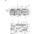
- FIG. 1 is a cross-sectional view and a partially enlarged view of the resin substrate 10 as viewed from the side.
- the resin substrate 10 includes a substrate portion 1 and an electronic component (first electronic component) 4.
- the substrate unit 1 has an upper main surface 2 and a lower main surface 3.
- the upper main surface 2 is a component mounting surface.
- the lower main surface 3 is an external mounting surface of the resin substrate 10.
- the electronic component 4 is surface-mounted on the upper main surface 2 of the substrate unit 1. Note that the electronic component 4 may be mounted on the substrate unit 1 in a state where the electronic component 4 is entirely or partially embedded (built-in) in the substrate unit 1. Moreover, the electronic component 4 does not need to be provided.
- the substrate unit 1 includes at least one layer of a flat film-like insulating base material 5. At least one layer of all the insulating substrates 5 includes a resin 6 and a plurality of conductive particles 7 mixed with the resin 6. Such an insulating substrate 5 corresponds to the “first insulating substrate” of the present invention.
- substrate part 1 is provided with the insulating base material 5 of a total of four layers, and the insulating base material 5 of all four layers is equivalent to the 1st insulating base material.
- the conductive particles 7 have an electrical resistivity lower than the intrinsic electrical resistivity of the resin 6. Since a plurality of such conductive particles 7 are dispersed in the resin 6, each insulating base material 5 has a substantial electrical resistivity lower than the inherent electrical resistivity of the resin 6. Thereby, the board
- FIG. 2 is a cross-sectional view showing an electronic apparatus 110 according to the present invention in which the resin substrate 10 is mounted on the external substrate 100.
- an electronic component first component provided on the external substrate 100 and electrically connected to the resin substrate 10.
- (2 electronic components) 101 may cause surge current to flow and cause electrostatic breakdown.
- the substrate portion 1 is difficult to be charged because the conductive particles 7 are mixed and the electrical resistivity is low. Therefore, when the electronic device 110 is manufactured, it is possible to suppress the occurrence of electrostatic breakdown due to a surge current flowing from the resin substrate 10 to the electronic component 101 via the external substrate 100. That is, the electronic device 110 can be manufactured at a high yield rate by suppressing the occurrence of electrostatic breakdown in the electronic component 101 due to charging of the resin substrate 10.
- the substrate unit 1 includes a plurality of conductor patterns 8 and via conductors 9.
- the plurality of conductor patterns 8 are provided on the main surface of each insulating substrate 5 in a shape separated from each other.
- the via conductor 9 directly conducts one of the sets of conductor patterns 8 opposed in the substrate thickness direction between different main surfaces of the insulating base material 5.
- the plurality of conductor patterns 8 are two conductors adjacent to each other in the main surface parallel direction without being directly connected to each other on the same main surface of any one of the insulating substrates 5 corresponding to the first insulating substrate. It includes a set of patterns 8.
- the plurality of conductor patterns 8 include a set of conductor patterns 8 that face each other in the substrate thickness direction without direct conduction between different main surfaces of the insulating base material 5 corresponding to the first insulating base material. .
- the position where the above-mentioned conductor patterns 8 are not directly connected to each other and the adjacent interval in the parallel direction of the main surface is the narrowest is A1
- the interval dimension at the position A1 is L1.
- a position where the distance between the conductor patterns 8 facing each other in the substrate thickness direction without being directly connected to each other in the substrate thickness direction is A2, and a distance dimension at the position A2 is L2.
- interval dimension L1 in position A1 is made larger than the space
- the plurality of conductive particles 7 include a shape having a longitudinal direction indicated by a broken line in the drawing.
- Each of the plurality of conductive particles 7 depends on the material and the granule manufacturing method, but has a variety of shapes such as a spherical shape, a column shape, a needle shape, a foil shape, or a shape in which they are aggregated. Can exist.
- the plurality of conductive particles 7 tend to be oriented in the longitudinal direction along the direction parallel to the main surface of the insulating substrate 5.
- the number of the conductive particles 7 whose longitudinal direction is closer to the direction parallel to the main surface of the insulating base 5 than the substrate thickness direction is longer than the substrate thickness direction.
- the number tends to be larger than the number of conductive particles 7 facing the angle. The cause of such a tendency is in the method for manufacturing the resin substrate 10 as described below.
- FIG. 3 is a diagram illustrating a manufacturing flow of the resin substrate 10.
- FIG. 4 is a schematic diagram showing a part of the manufacturing process of the resin substrate 10.
- FIG. 5 is a cross-sectional view showing a state in the manufacturing process of the resin substrate 10.
- the conductor pattern 8 is formed by using the subtractive method.
- the conductor pattern is formed by forming a metal film on the resist and removing the resist, using a known semi-additive method. It is also possible to adopt a construction method. Further, in the following description, only a portion that becomes a single resin substrate 10 will be described. And it is good to manufacture the some resin substrate 10 at once by cutting out from a raw fabric sheet.
- the resin 6 is a thermoplastic resin will be described as an example.
- the conductive particles 7 are put into the stirring tank 103 together with the resin paste 107 to be the resin 6 later, and the resin paste 107 and the conductive particles 7 are mixed in the stirring tank 103. Are mixed together (see FIGS. 3 and 4: S1).
- the conductive particles 7 are introduced into the stirring vessel 103 after the weight ratio is adjusted so that the electrical resistivity of the insulating substrate 5 is about 1 M ⁇ ⁇ cm.
- the resin 6 is made of any resin material such as liquid crystal polymer resin, PEEK (polyetheretherketone), PEI (polyetherimide), PPS (poniphenylene sulfide), PI (polyimide), and the like. it can.
- the liquid crystal polymer resin has flexibility, thermoplasticity, and the like.
- the resin substrate 10 can have appropriate insulation and flexibility. it can.
- the resin paste 107 may be a mixture of powdered resin 6 in a binder or the like, or a melted resin 6 having thermoplasticity.
- the conductive particles 7 can be made of any conductive material, for example, an iron-based material such as permalloy or ferrite, pure iron, carbon, or the like. Of these conductive materials, it is particularly preferable to use carbon that has high chemical stability and is unlikely to change in electrical resistivity due to oxidation or reduction.
- the above-described resin paste 107 is formed into a sheet (see FIGS. 3 and 4: S2).
- the resin paste 107 is applied on the carrier film 104, and the resin paste 107 is drawn out to the doctor blade 105 together with the carrier film 104, thereby forming the resin paste 107 to a constant thickness.
- the resin paste 107 spreads in the direction parallel to the main surface due to the external force applied to the resin paste 107 from the doctor blade 105 or the like, or the weight of the resin paste 107, etc. Flow occurs. By this flow, the conductive particles 7 inside the resin sheet 108 are likely to be oriented such that the main surface parallel direction is the longitudinal direction.
- a metal foil 106 on which the conductor pattern 8 will be formed later is attached to both surfaces or one surface of the resin sheet 108 by a hot press or the like, thereby forming the resin sheet 108 in a state in which the metal foil 106 is adhered ( 3 and 5: see S4).
- the metal foil 106 can also be affixed on the single side
- the conductor pattern 8 and the via conductor 9 are formed on the resin sheet 108, and the insulating substrate 5 is formed from the resin sheet 108 (see FIGS. 3 and 5: S5).
- the metal foil 106 is masked with an etching resist.
- the metal foil 106 exposed from the etching resist is removed by etching.
- the etching resist is washed. In this way, the conductor pattern 8 can be formed.
- the via conductor 9 can be formed by forming a through hole in the resin sheet 108 and performing electroless plating on the inner wall of the through hole, or by filling the through hole with a conductive paste to be metallized. it can.
- a plurality of insulating base materials 5 formed as described above are prepared and stacked in an aligned state. Then, by heating and pressing from the substrate thickness direction, the respective insulating base materials 5 made of thermoplastic resin are brought into close contact with each other to form the substrate portion 1 in which the plurality of insulating base materials 5 are integrated (FIGS. 3 and 5: (See S6).
- the via conductor 9 described above may be metallized by a hot press in this step.
- the via conductor 9 can be directly joined to the conductor pattern 8 provided on the main surface of the different insulating base material 5, and the reliability and robustness of the connection between the via conductor 9 and the conductor pattern 8 are improved. be able to.
- the insulating substrate 5 extends in the direction parallel to the main surface due to tension acting on the carrier film 104, external force applied through the doctor blade 105, the metal foil 106, and the other insulating substrate 5. Such deformation occurs. This also makes it easy for the conductive particles 7 to be oriented in the direction parallel to the principal surface inside the insulating substrate 5.
- the electronic component 4 is surface-mounted on the board 1 (see FIGS. 3 and 5: S7).
- the terminal electrode of the electronic component 4 may be soldered to the conductor pattern 8 using a reflow method or the like in a state where the electronic component 4 is mounted on the substrate unit 1.
- the terminal electrode of the electronic component 4 may be bonded to the conductor pattern 8 via a bump or the like by ultrasonic bonding or the like.
- a resist film that covers the main surface of the substrate portion 1 while exposing the conductor pattern 8 may be formed before mounting the electronic component 4.
- this step (S7) if the charge amount of the substrate unit 1 is large, a surge current flows through the electronic component 4 mounted on the substrate unit 1, and there is a possibility that the electronic component 4 may be electrostatically damaged.
- the conductive particles 7 are mixed with the substrate portion 1 and the electrical resistivity is low, the substrate portion 1 is difficult to be charged and electrostatic damage of the electronic component 4 can be suppressed.
- the resin substrate 10 can be manufactured using the manufacturing method as described above.
- the longitudinal direction of the inside conductive particles 7 faces the direction parallel to the main surface of the insulating substrate 5 in the flat film-like insulating substrate 5 (resin sheet). Such an action works in various processes.
- the conductive patterns 8 adjacent to each other in the direction parallel to the main surface of the insulating substrate 5 are likely to be short-circuited via the conductive particles 7. Therefore, in the resin substrate 10, as described above with reference to FIG. 1, adjacent conductive patterns 8 are not directly connected to each other on the same main surface of the insulating base material 5 corresponding to the first insulating base material.
- the distance L1 between the conductor patterns 8 facing each other without direct conduction between different main surfaces of the insulating base material 5 corresponding to the first insulating base material is set to the distance dimension L1 at the position A1 where the distance between them is the narrowest. Is made larger than the interval dimension L2 at the position A2 where the distance becomes the narrowest.
- the resin substrate 10 can be manufactured at a high yield rate by suppressing the occurrence of defects such as a short circuit between the conductor patterns 8.
- the manufacturing method mentioned above is an example to the last, and the resin substrate 10 can be manufactured even if it is another manufacturing method. Whatever manufacturing method is used, the step of forming a resin sheet into a flat film and the step of laminating other members in the substrate thickness direction of the insulating base are necessary. The tendency for the longitudinal direction of the conductive particles to be in the direction parallel to the main surface cannot be avoided. Therefore, no matter what manufacturing method the resin substrate 10 is manufactured, the configuration in which the interval dimension between the conductor patterns is set as described above is effective for suppressing a short circuit between the conductor patterns.
- the resin substrate of this invention is not restricted to such a structure, 4 layers It can also be configured as a multi-layer substrate having a different number of layers from the above, or as a single-layer substrate.
- the conductive particles may be mixed with only some of the insulating substrates. In that case, you may make it set the space
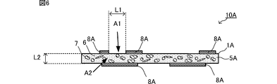
- FIG. 6 is a schematic cross-sectional view of the resin substrate 10A.
- Resin substrate 10A includes a substrate portion 1A.
- the substrate unit 1A is composed of only one flat film-like insulating base material 5A.
- the insulating base 5A includes a resin 6 and a plurality of conductive particles 7 mixed with the resin 6, and corresponds to a “first insulating base”. Since a plurality of conductive particles 7 are dispersed in the resin 6, the insulating base material 5 ⁇ / b> A has a substantial electrical resistivity lower than the intrinsic electrical resistivity of the resin 6, and is difficult to be charged. ing.
- the substrate portion 1A includes a plurality of conductor patterns 8A.
- the plurality of conductor patterns 8A are provided on the main surface of the insulating base 5A in a shape separated from each other. Further, the plurality of conductor patterns 8A are not directly connected to each other between a set of adjacent conductor patterns 8A and different main surfaces of the insulating base 5A without being directly connected to each other on the same main surface of the insulating base 5A. And a set of opposing conductor patterns 8A.
- the interval dimension L1 at the position A1 where the interval in the parallel direction of the main surface between the adjacent conductor patterns 8A is not directly conducted on the same main surface of the insulating base 5A is the insulating base.
- the distance between the opposing conductor patterns 8A in the thickness direction of the substrate between the different principal surfaces of the material 5A in the substrate thickness direction is larger than the distance dimension L2 at the position A2.
- the conductive particles 7 tend to be oriented in the longitudinal direction in the main surface parallel direction of the insulating base material 5A. Therefore, by making the interval dimension L1 at the position A1 larger than the interval dimension L2 at the position A2, it is possible to suppress a short circuit between the conductor patterns 8A adjacent in the main surface parallel direction via the conductive particles 7. be able to. Therefore, the resin substrate 10A can be manufactured at a high yield rate by suppressing the occurrence of defects such as a short circuit between the conductor patterns 8A.
- the substrate portion is configured by laminating a plurality of insulating base materials, but a case where conductive particles are mixed only with some insulating base materials is shown.
- FIG. 7 is a schematic cross-sectional view of the resin substrate 10B.
- Resin substrate 10B includes a substrate portion 1B.
- the substrate portion 1B is configured by laminating two layers of a flat film-like insulating base material 5B and two layers of a flat film-like insulating base material 15B.
- the insulating substrate 5B includes a resin 6 and a plurality of conductive particles 7 mixed with the resin 6, and corresponds to a “first insulating substrate”.
- the insulating base material 15 ⁇ / b> B includes only the resin 6.
- the insulating base material 5B has a plurality of conductive particles 7 dispersed in the resin 6, so that the substantial electrical resistivity is the intrinsic electrical resistivity of the resin 6, that is, the electrical resistance of the insulating base material 15B. It is lower than the rate. Even in such a configuration, the resin substrate 10B has the insulating base material 5B having a low electrical resistivity, and therefore is less likely to be charged than when the insulating base material 5B is not provided.
- the board portion 1B includes a plurality of conductor patterns 8B and 18B and via conductors 9B.
- the plurality of conductor patterns 8B are provided along the main surface of the insulating base material 5B in a shape separated from each other.
- the plurality of conductor patterns 18B are separated from each other, do not follow the main surface of the insulating base material 5B, and are provided only along the main surface of the insulating base material 15B.
- the plurality of conductor patterns 8B are directly connected to each other between a set of adjacent conductor patterns 8B and different main surfaces of the insulating base 5B without being directly connected to each other on the same main surface of the insulating base 5B. And a set of conductor patterns 8B facing each other.
- the interval dimension L1 at the position A1 in which the interval in the parallel direction of the main surface between the adjacent conductor patterns 8B is not directly conducted on the same main surface of the insulating base 5B is the insulating base.
- the interval in the substrate thickness direction between the opposing conductor patterns 8B is made larger than the interval dimension L2 at the narrowest position A2 without direct conduction between different main surfaces of the material 5B.
- the conductive particles 7 tend to have the longitudinal direction in the main surface parallel direction of the insulating base material 5B. Therefore, by making the interval dimension L1 at the position A1 larger than the interval dimension L2 at the position A2, it is possible to suppress a short circuit between the conductor patterns 8B adjacent in the main surface parallel direction via the conductive particles 7. be able to. Therefore, the resin substrate 10B can be manufactured at a high yield rate while suppressing the occurrence of defects such as short-circuiting between the conductor patterns 8B.
- the interval between the plurality of conductor patterns 18B may be narrower than the interval dimensions L1 and L2 described above.
- the interval between the conductive patterns 8B directly connected via the via conductor 9B may be narrower than the interval dimensions L1 and L2.
- the conductive particles 7 may be magnetic particles such as permalloy, and the coil pattern may be provided on the insulating substrate 5B. In this way, a large inductance can be obtained even if the size of the coil pattern is reduced.
Landscapes
- Engineering & Computer Science (AREA)
- Microelectronics & Electronic Packaging (AREA)
- Manufacturing & Machinery (AREA)
- Production Of Multi-Layered Print Wiring Board (AREA)
- Structure Of Printed Boards (AREA)
- Laminated Bodies (AREA)
Abstract
樹脂基板(10)は、複数の導電性粒子(7)が樹脂(6)に混ぜあわされた絶縁性基材(5)と、絶縁性基材(5)の主面に設けられた複数の導体パターン(8)と、を備える。絶縁性基材(5)の同一の主面上で2つの導体パターン(8)が互いに直接導通することなく隣接する間隔が最も狭い位置での間隔寸法を(L1)とし、絶縁性基材(5)の異なる主面間で2つの導体パターン(8)が互いに直接導通することなく対向する間隔が最も狭い位置での間隔寸法を(L2)とすると、(L1)は(L2)以上である(L1≧L2)。
Description
本発明は、絶縁性基材の主面に複数の導体パターンが形成された樹脂基板と、その樹脂基板を備えた電子機器と、に関する。
従来、金属粒子が混練された樹脂を用いて樹脂基板が構成されることがあった(例えば特許文献1および2参照。)。
特許文献1に開示された樹脂基板は、コイルパターンを構成する導体パターンを備えている。該樹脂基板において、コイルパターンが構成される部分の樹脂層には、磁性金属粒子が混ぜられている。このことにより、コイルパターンは、サイズが小さくても、通常よりも大きなインダクタンスを有するものになる。
特許文献2に開示された樹脂基板は、ESD(静電気放電破壊)保護のための構造を備えている。具体的には、該樹脂基板は、内部に設けられた空洞部と、空洞部に露出した状態で間隔を空けて互いに対向する信号ライン側の導体パターンおよびグランドライン側の導体パターンとを備えている。そして、空洞部の近傍の樹脂層に導電性粒子が混ぜられている。この樹脂基板は、静電気放電等によって信号ラインにサージ電流が流れると、空洞部において信号ライン側の導体パターンとグランドライン側の導体パターンとの間に放電を生じる。これにより、該樹脂基板では、サージ電流を信号ラインからグランドラインに逃がすことができる。
従来の樹脂基板は、樹脂基板を構成する樹脂材料によっては容易に帯電が生じ、電子部品を樹脂基板に搭載する際や、樹脂基板を電子機器に搭載する際に、電子部品や電子機器に静電破壊を生じさせることがあった。前述の特許文献2に記載された構成では、信号ラインに流れるサージ電流をグランドに逃がすことはできるが、樹脂基板自体の帯電は防ぐことが難しかった。
そこで、樹脂基板を帯電しにくくするために、樹脂基板において絶縁性を保ったまま実質的な電気抵抗率を低くすることが考えられる。具体的には、従来技術のように導電性粒子を樹脂に混ぜあわせることが考えられる。しかしながら、単に導電性粒子を樹脂に混ぜあわせるだけでは、樹脂基板の製造過程で時として導電性粒子が変形する等により、導体パターン間が短絡してしまう不良の発生率が高くなってしまう。
そこで、本発明の目的は、帯電しにくく、かつ、導体パターン間が短絡してしまう不良の発生を抑制できる樹脂基板と、その樹脂基板を備えた電子機器と、を提供することにある。
この発明の樹脂基板は、基板厚み方向に対向する一対の主面を有する少なくとも1以上の絶縁性基材と、前記絶縁性基材の主面に形成された複数の導体パターンと、を備え、前記絶縁性基材は、複数の導電性粒子が樹脂に混ぜあわされた第1絶縁性基材を含み、前記複数の導体パターンのうちの少なくとも2つは、前記第1絶縁性基材の同一の主面上で互いに直接導通することなく隣接し、前記複数の導体パターンのうちの少なくとも2つは、前記第1絶縁性基材の異なる主面間で互いに直接導通することなく対向し、前記第1絶縁性基材の同一の主面上で互いに直接導通することなく隣接する前記導体パターン同士の間隔が最も狭くなる位置での間隔寸法は、前記第1絶縁性基材の異なる主面間で互いに直接導通することなく対向する前記導体パターン同士の間隔が最も狭くなる位置での間隔寸法以上である。特には、前記第1絶縁性基材の同一の主面上で互いに直接導通することなく隣接する前記導体パターン同士の間隔が最も狭くなる位置での間隔寸法は、前記第1絶縁性基材の異なる主面間で互いに直接導通することなく対向する前記導体パターン同士の間隔が最も狭くなる位置での間隔寸法より大きいことが好ましい。
これらの構成では、導電性粒子によって、絶縁性基材の実質的な電気抵抗率を低くすることができ、基板部を帯電しにくくすることができる。ただし、複数の導電性粒子が絶縁性基材に混ぜあわされていると、導電性粒子の長手方向が絶縁性基材の主面平行方向に向き易くなる。このため、絶縁性基材の同一主面上で隣接する導体パターンの間が導電性粒子によって短絡され易くなってしまう。これに対し、上記構成では、絶縁性基材の同一主面上で隣接する導体パターン同士の最小間隔を広くするので、導体パターンの間が導電性粒子によって短絡されるような不良の発生を抑制することができる。
前記複数の導電性粒子は、いずれかの方向において他の部分よりも径が長い部分を有するものを含んでもよい。また、前記導電性粒子はカーボンを含んでいてもよい。
複数の導電性粒子が上記の形状のものを含むことで、導電性粒子の長手方向が絶縁性基材の主面平行方向に向き易くなるので、本発明の構成が特に有効となる。そして、カーボンはそのような導電性粒子の具体的な材料の一例である。また、カーボンは、一般的な樹脂材料よりは電気抵抗率が低いため、樹脂基板の絶縁性を保ったまま樹脂基板の実質的な電気抵抗率を低減するために樹脂に混ぜあわせる材料として適している。また、カーボンは化学的安定性が高く、この点でも樹脂に混ぜあわせる材料として適している。
複数の前記絶縁性基材を積層していてもよい。この場合、前記複数の絶縁性基材は、熱可塑性樹脂を含むことが好ましい。この構成では、複数の絶縁性基材を加熱プレスすることで一体化することができる。
前記絶縁性基材に内蔵または搭載された第1電子部品を更に備えることが好ましい。
この構成では、絶縁性基材の帯電による第1電子部品での静電破壊の発生を抑制し、高い良品率で樹脂基板を製造することができる。
この発明の電子機器は、上述の樹脂基板と、前記樹脂基板を搭載した構造体と、前記構造体に搭載され、前記樹脂基板と電気的に接続された第2電子部品と、を備えることが好ましい。
この構成では、樹脂基板の帯電による第2電子部品での静電破壊の発生を抑制し、高い良品率で電子機器を製造することができる。
この発明によれば、導電性粒子を樹脂に混ぜ合わせることによって、絶縁性基材の実質的な電気抵抗率を低くすることができ、樹脂基板を帯電しにくくすることができる。また、導電性粒子を樹脂に混ぜ合わせた第1絶縁性基材の同一の主面上で隣接する導体パターン同士の間隔を広くするので、第1絶縁性基材に混ぜあわされる導電性粒子によって導体パターンの間が短絡するような不良の発生を抑制できる。
以下、本発明の第1の実施形態に係る樹脂基板10について説明する。図1は、樹脂基板10を側面側から見た断面図および部分拡大図である。
樹脂基板10は、基板部1と電子部品(第1電子部品)4とを備えている。基板部1は、上主面2と下主面3とを有している。上主面2は、部品搭載面である。下主面3は、当該樹脂基板10の外部実装面である。電子部品4は、基板部1の上主面2に表面実装されている。なお、電子部品4は、全体または一部が基板部1に埋め込まれた(内蔵)状態で、基板部1に搭載されていてもよい。また、電子部品4は設けられていなくてもよい。
基板部1は、少なくとも1層以上の平膜状の絶縁性基材5を備えている。全ての絶縁性基材5のうち、少なくとも1層は、樹脂6と、樹脂6に混ぜあわされた複数の導電性粒子7とを備えている。このような絶縁性基材5が本発明の「第1絶縁性基材」に相当する。本実施形態では、基板部1は、合計4層の絶縁性基材5を備え、4層全ての絶縁性基材5が第1絶縁性基材に相当している。
導電性粒子7は、樹脂6の固有の電気抵抗率よりも低い電気抵抗率を持つものである。このような導電性粒子7が樹脂6中に複数分散していることにより、各絶縁性基材5は、実質的な電気抵抗率が樹脂6の固有の電気抵抗率よりも低いものになる。これにより、基板部1は、各絶縁性基材5が導電性粒子7を含まずに樹脂6のみで構成される場合よりも、帯電しにくくなっている。
図2は、外部基板100に樹脂基板10を搭載してなる本発明の電子機器110を示す断面図である。外部基板100のような構造体に樹脂基板10を搭載する際、仮に基板部1の帯電量が大きければ、外部基板100上に設けられて樹脂基板10と電気的に接続される電子部品(第2電子部品)101にサージ電流が流れて静電破壊が生じる恐れがある。しかしながら、基板部1は、導電性粒子7が混ぜあわされていて電気抵抗率が低いので、帯電しにくい。したがって、この電子機器110を製造する際、外部基板100を介して樹脂基板10から電子部品101にサージ電流が流れて静電破壊が生じることを抑止することができる。すなわち、この電子機器110は、樹脂基板10の帯電による電子部品101での静電破壊の発生を抑制し、高い良品率で製造することができる。
また、図1中に示すように、基板部1は、複数の導体パターン8とビア導体9とを備えている。複数の導体パターン8は、それぞれ互いに分離した形状で、各絶縁性基材5の主面に設けられている。ビア導体9は、絶縁性基材5の異なる主面間で、基板厚み方向に対向する導体パターン8の組のうちの一つを直接導通させる。
ここで、複数の導体パターン8は、第1絶縁性基材に相当するいずれかの絶縁性基材5の同一主面上で、互いに直接導通することなく主面平行方向に隣接する2つの導体パターン8の組を含んでいる。また、複数の導体パターン8は、第1絶縁性基材に相当する絶縁性基材5の異なる主面間で、直接導通することなく基板厚み方向に対向する導体パターン8の組を含んでいる。以下、上記した導体パターン8同士が互いに直接導通することなく主面平行方向に隣接する間隔が最も狭い位置をA1とし、位置A1における間隔寸法をL1とする。また、上記した導体パターン8同士が互いに直接導通することなく基板厚み方向に対向する間隔が最も狭い位置をA2とし、位置A2における間隔寸法をL2とする。そして、この基板部1においては、位置A1での間隔寸法L1を、位置A2での間隔寸法L2よりも大きくしている。
また、図1中で拡大して示すように、複数の導電性粒子7は、図中に破線で示す長手方向を有する形状のものを含んでいる。複数の導電性粒子7それぞれは、その材質や粒体製造工法にもよるが、球状や、柱状、針状、箔状、またはそれらが凝集した形状など多様な形状で絶縁性基材5内に存在しうる。
ただし、複数の導電性粒子7は、絶縁性基材5の主面平行方向に沿って長手方向が向きやすい傾向を有する。例えば、複数の導電性粒子7のうち、長手方向が基板厚み方向よりも絶縁性基材5の主面平行方向に近い角度を向く導電性粒子7の数が、長手方向が基板厚み方向に近い角度を向く導電性粒子7の数よりも多くなり易い。このような傾向が生じる要因は、次に説明するような樹脂基板10の製造方法にある。
図3は、樹脂基板10の製造フローを例示する図である。図4は、樹脂基板10の製造過程の一部を示す模式図である。図5は、樹脂基板10の製造過程での状態を示す断面図である。
なお、以下では、サブトラクティブ法を用いて導体パターン8を形成する場合について説明するが、公知のセミアディティブ法、すなわち、レジスト上に金属膜を形成して、レジストを取り除くことで導体パターンを成形する工法を採用することもできる。また、以下の説明では単一の樹脂基板10となる部分のみについて説明するが、実際には、広大な原反シートに、複数の樹脂基板10を主面平行方向に縦横に配列した状態で製造し、原反シートから切りだすことで複数の樹脂基板10を一度に製造するとよい。また、以下、樹脂6を熱可塑性樹脂とする場合を例に説明する。
サブトラクティブ法を用いる樹脂基板10の製造方法では、まず、後に樹脂6となる樹脂ペースト107とともに導電性粒子7を撹拌槽103に投入し、撹拌槽103にて樹脂ペースト107と導電性粒子7とを混ぜあわせる(図3,4:S1参照)。導電性粒子7は、後に絶縁性基材5の電気抵抗率が1MΩ・cm程度となるように、その重量比を調整して撹拌槽103に投入される。なお、樹脂6は、任意の樹脂材料、例えば、液晶ポリマ樹脂、PEEK(ポリエーテルエーテルケトン)、PEI(ポリエーテルイミド)、PPS(ポニフェニレンスルファイド)、PI(ポリイミド)など、を用いることができる。例えば液晶ポリマ樹脂は、可撓性、熱可塑性等を有するものであり、液晶ポリマ樹脂を用いて樹脂基板10を構成すると、樹脂基板10に適切な絶縁性と可撓性とを持たせることができる。樹脂ペースト107は、粉体状の樹脂6をバインダー等に混ぜたものでもよく、熱可塑性を持つ樹脂6を溶融させたものでもよい。また、導電性粒子7は、任意の導電性材料、例えば、パーマロイやフェライト等の鉄系材料、純鉄、カーボンなど、を用いることができる。これらの導電性材料のうちでは、化学的安定性が高く、酸化や還元による電気抵抗率の変化が生じにくいカーボンを用いることが特に好ましい。
次に、前述した樹脂ペースト107をシート状に成形する(図3,4:S2参照)。例えば、樹脂ペースト107を、キャリアフィルム104上に塗布し、キャリアフィルム104とともに樹脂ペースト107をドクターブレード105に引き出すことにより、樹脂ペースト107を一定の厚みに成形する。
次に、一定の厚みに成形された樹脂ペースト107に熱処理等を施し、樹脂ペースト107を固化させ、樹脂シート108を形成する(図3,5:S3参照)。
上記のように樹脂シート108を成膜する工程(S2)では、ドクターブレード105などから樹脂ペースト107に加わる外力や、樹脂ペースト107の自重などによって、樹脂ペースト107に主面平行方向に拡がるような流動が生じる。この流動により、樹脂シート108の内部の導電性粒子7には、主面平行方向を長手方向とするような配向が生じ易くなる。
次に、樹脂シート108の両面または片面に、後に導体パターン8が形成される金属箔106を加熱プレス等により貼り付け、これにより金属箔106が貼り付けられた状態の樹脂シート108を形成する(図3,5:S4参照)。なお、前述したキャリアフィルム104に予め金属箔106を貼り付けておくことにより、樹脂シート108の片面に金属箔106を貼り付けることもできる。
次に、樹脂シート108に導体パターン8やビア導体9を形成し、樹脂シート108から絶縁性基材5を形成する(図3,5:S5参照)。例えば、サブトラクティブ法を用いる場合には、金属箔106をエッチングレジストでマスキングする。次に、エッチングレジストから露出する金属箔106をエッチングにより除去する。そして、エッチングレジストを洗浄する。このようにして、導体パターン8を成形することができる。
また、樹脂シート108に貫通孔を形成して、貫通孔の内壁に無電解メッキを施したり、貫通孔に導体ペーストを充填して金属化させたりすることで、ビア導体9を形成することができる。
次に、上記のようにして形成された絶縁性基材5を複数用意し、位置合わせした状態で積み重ねる。そして、基板厚み方向から加熱プレスすることにより、熱可塑性樹脂からなる各絶縁性基材5を密着させ、複数の絶縁性基材5を一体化した基板部1を形成する(図3,5:S6参照)。
なお、前述したビア導体9は、この工程での加熱プレスにより金属化させてもよい。この場合、ビア導体9を、異なる絶縁性基材5の主面に設けられた導体パターン8に直接接合させることができ、ビア導体9と導体パターン8との接続の確実性および頑健性を高めることができる。
上記した各種の工程では、キャリアフィルム104に働く張力や、ドクターブレード105や金属箔106、他の絶縁性基材5を介して加わる外力などによって、絶縁性基材5に主面平行方向に伸びるような変形が生じる。このことによっても、絶縁性基材5の内部では、導電性粒子7に主面平行方向を長手とするような配向が生じ易くなる。
次に、基板部1に電子部品4を表面実装する(図3,5:S7参照)。例えば、基板部1に電子部品4を搭載した状態で、リフロー法などを用いて電子部品4の端子電極を導体パターン8にはんだ付けするとよい。また、超音波接合等により、電子部品4の端子電極をバンプ等を介して導体パターン8に接合してもよい。また、電子部品4を搭載する前に、導体パターン8を露出させながら基板部1の主面を覆うレジスト膜を成膜してもよい。
この工程(S7)で、仮に基板部1の帯電量が大きければ、基板部1に実装される電子部品4にサージ電流が流れ、電子部品4に静電破壊が生じる恐れがある。しかしながら、本実施形態では基板部1に導電性粒子7が混ぜあわされていて電気抵抗率が低いので、基板部1が帯電しにくく、電子部品4の静電破壊を抑止することができる。
以上のような製造方法を用いて樹脂基板10は製造することができる。このような製造方法が採用されることにより、平膜状の絶縁性基材5(樹脂シート)には、内部の導電性粒子7の長手方向が絶縁性基材5の主面平行方向を向くような作用が各種の工程で働く。
したがって、何らの対策も施さなければ絶縁性基材5の主面平行方向に隣接する導体パターン8間が、導電性粒子7を介して短絡しやすくなってしまう。そこで、該樹脂基板10においては、図1を用いて前述したように、第1絶縁性基材に相当する絶縁性基材5の同一主面上で互いに直接導通することなく隣接する導体パターン8同士の間隔が最も狭くなる位置A1での間隔寸法L1を、第1絶縁性基材に相当する絶縁性基材5の異なる主面間で互いに直接導通することなく対向する導体パターン8同士の間隔が最も狭くなる位置A2での間隔寸法L2よりも大きくする。このことにより、第1絶縁性基材に相当する絶縁性基材5においては、主面平行方向に隣接する導体パターン8間が、導電性粒子7を介して短絡することを抑止することができる。したがって、樹脂基板10は、導体パターン8の間が短絡するような不良の発生を抑制して高い良品率で製造することができる。
なお、上述した製造方法はあくまで一例であり、樹脂基板10はその他の製造方法であっても製造することができる。どのような製造方法であっても、平膜状に樹脂シートを成膜する工程や、絶縁性基材の基板厚み方向に他部材を積層する工程は必要となるために、絶縁性基材において導電性粒子の長手方向が主面平行方向を向く傾向を避けることができない。したがって、どのような製造方法で樹脂基板10が製造されていたとしても、上述したように導体パターン間の間隔寸法を設定する構成は、導体パターン間の短絡を抑止するために有効である。
また、この実施形態においては、樹脂基板10として4層の第1絶縁性基材を積層した構成を開示したが、本発明の樹脂基板は、このような構成に限られるものではなく、4層とは異なる層数の多層基板として、または単層の基板として構成することもできる。また導電性粒子を全ての絶縁性基材に混ぜあわせる他にも、一部の絶縁性基材のみに導電性粒子を混ぜあわせるようにしてもよい。その場合には、導電性粒子を混ぜあわせる絶縁性基材においてのみ、上述した導体パターン間の間隔寸法を設定するようにしてもよい。
次に、本発明の第2の実施形態に係る樹脂基板10Aについて説明する。本実施形態は、基板部を1層の絶縁性基材で構成する場合を示す。
図6は、樹脂基板10Aの模式断面図である。
樹脂基板10Aは、基板部1Aを備えている。基板部1Aは、1層の平膜状の絶縁性基材5Aのみで構成されている。絶縁性基材5Aは、樹脂6と、樹脂6に混ぜあわされた複数の導電性粒子7とを備え、「第1絶縁性基材」に相当する。導電性粒子7が樹脂6中に複数分散していることにより、絶縁性基材5Aは、実質的な電気抵抗率が樹脂6の固有の電気抵抗率よりも低いものになり、帯電しにくくなっている。
また、基板部1Aは、複数の導体パターン8Aを備えている。複数の導体パターン8Aは、それぞれ互いに分離した形状で、絶縁性基材5Aの主面に設けられている。また、複数の導体パターン8Aは、絶縁性基材5Aの同一主面上で互いに直接導通することなく隣接する導体パターン8Aの組と、絶縁性基材5Aの異なる主面間で、互いに直接導通することなく対向する導体パターン8Aの組とを含んでいる。
そして、ここでも、絶縁性基材5Aの同一主面上で互いに直接導通することなく隣接する導体パターン8A間の主面平行方向の間隔が最も狭い位置A1での間隔寸法L1は、絶縁性基材5Aの異なる主面間で互いに直接導通することなく対向する導体パターン8A間の基板厚み方向での間隔が最も狭い位置A2での間隔寸法L2よりも大きくしている。
このような構成の樹脂基板10Aにおいても、導電性粒子7に絶縁性基材5Aの主面平行方向を長手方向が向くような傾向が生じる。したがって、位置A1での間隔寸法L1を位置A2での間隔寸法L2よりも大きくすることにより、主面平行方向に隣接する導体パターン8A間が、導電性粒子7を介して短絡することを抑止することができる。したがって、樹脂基板10Aは、導体パターン8Aの間が短絡するような不良の発生を抑制して高い良品率で製造することができる。
次に、本発明の第3の実施形態に係る樹脂基板10Bについて説明する。本実施形態は、基板部を複数の絶縁性基材を積層して構成するが、一部の絶縁性基材のみに導電性粒子を混ぜあわせる場合を示す。
図7は、樹脂基板10Bの模式断面図である。
樹脂基板10Bは、基板部1Bを備えている。基板部1Bは、2層の平膜状の絶縁性基材5Bと2層の平膜状の絶縁性基材15Bとを積層して構成されている。絶縁性基材5Bは、樹脂6と、樹脂6に混ぜあわされた複数の導電性粒子7とを備え、「第1絶縁性基材」に相当する。絶縁性基材15Bは、樹脂6のみを備える。絶縁性基材5Bは、導電性粒子7が樹脂6中に複数分散していることにより、実質的な電気抵抗率が樹脂6の固有の電気抵抗率、すなわち、絶縁性基材15Bの電気抵抗率よりも低いものになっている。このような構成であっても、樹脂基板10Bは、電気抵抗率が低い絶縁性基材5Bを有しているので、絶縁性基材5Bを有しない場合よりも帯電しにくくなっている。
また、基板部1Bは、複数の導体パターン8B,18Bとビア導体9Bとを備えている。複数の導体パターン8Bは、それぞれ互いに分離した形状で、絶縁性基材5Bの主面に沿って設けられている。複数の導体パターン18Bは、それぞれ互いに分離した形状で、絶縁性基材5Bの主面には沿わず、絶縁性基材15Bの主面のみに沿って設けられている。また、複数の導体パターン8Bは、絶縁性基材5Bの同一主面上で互いに直接導通することなく隣接する導体パターン8Bの組と、絶縁性基材5Bの異なる主面間で互いに直接導通することなく対向する導体パターン8Bの組とを含んでいる。
そして、ここでも、絶縁性基材5Bの同一主面上で互いに直接導通することなく隣接する導体パターン8B間の主面平行方向の間隔が最も狭い位置A1での間隔寸法L1は、絶縁性基材5Bの異なる主面間で互いに直接導通することなく対向する導体パターン8B間の基板厚み方向での間隔が最も狭い位置A2での間隔寸法L2よりも大きくしている。
このような構成の樹脂基板10Bにおいても、導電性粒子7に絶縁性基材5Bの主面平行方向を長手方向とするような傾向が生じる。したがって、位置A1での間隔寸法L1を位置A2での間隔寸法L2よりも大きくすることにより、主面平行方向に隣接する導体パターン8B間が、導電性粒子7を介して短絡することを抑止することができる。したがって、樹脂基板10Bは、導体パターン8Bの間が短絡するような不良の発生を抑制して高い良品率で製造することができる。
なお、この構成では、導電性粒子7が混ぜあわされていない絶縁性基材15Bに設けられた複数の導体パターン18Bを備えているが、該複数の導体パターン18Bにおいては、導電性粒子7による短絡が生じる恐れはない。したがって、このような複数の導体パターン18B同士が互いに隣接する間隔は、前述した間隔寸法L1,L2より狭くてもよい。
また、導電性粒子7が混ぜあわされている絶縁性基材5Bに設けられた複数の導体パターン8B同士であったとしても、ビア導体9Bを介して直接接続されている導体パターン8B同士の場合には、導電性粒子7による短絡が生じても構わない。したがって、ビア導体9Bを介して直接接続されている導体パターン8B同士が対向する間隔も、前述した間隔寸法L1,L2より狭くてもよい。
また、この樹脂基板10Bにおいて、導体パターンからなるコイルパターンを形成する場合には、導電性粒子7をパーマロイのような磁性粒子とするとともに、絶縁性基材5Bにコイルパターンを設けるとよい。このようにすると、当該コイルパターンのサイズを小型にしても大きなインダクタンスを得ることができる。
最後に、前記実施形態の説明は、すべての点で例示であって、制限的なものではないと考えられるべきである。本発明の範囲は、上述実施形態ではなく、特許請求の範囲によって示される。さらに、本発明の範囲には、特許請求の範囲と均等の意味および範囲内でのすべての変更が含まれることが意図される。
1,1A,1B…基板部
2…上主面
3…下主面
4…電子部品
5,5A,5B,15B…絶縁性基材
6…樹脂
7…導電性粒子
8,8A,8B,18B…導体パターン
9,9B…ビア導体
10,10A,10B…樹脂基板
100…外部基板
101…電子部品
103…撹拌槽
104…キャリアフィルム
105…ドクターブレード
106…金属箔
107…樹脂ペースト
108…樹脂シート
110…電子機器
2…上主面
3…下主面
4…電子部品
5,5A,5B,15B…絶縁性基材
6…樹脂
7…導電性粒子
8,8A,8B,18B…導体パターン
9,9B…ビア導体
10,10A,10B…樹脂基板
100…外部基板
101…電子部品
103…撹拌槽
104…キャリアフィルム
105…ドクターブレード
106…金属箔
107…樹脂ペースト
108…樹脂シート
110…電子機器
Claims (8)
- 基板厚み方向に対向する一対の主面を有する少なくとも1以上の絶縁性基材と、
前記絶縁性基材の主面に形成された複数の導体パターンと、
を備え、
前記絶縁性基材は、複数の導電性粒子が樹脂に混ぜあわされた第1絶縁性基材を含み、
前記複数の導体パターンのうちの少なくとも2つは、前記第1絶縁性基材の同一の主面上で互いに直接導通することなく隣接し、
前記複数の導体パターンのうちの少なくとも2つは、前記第1絶縁性基材の異なる主面間で互いに直接導通することなく対向し、
前記第1絶縁性基材の同一の主面上で互いに直接導通することなく隣接する前記導体パターン同士の間隔が最も狭くなる位置での間隔寸法は、前記第1絶縁性基材の異なる主面間で互いに直接導通することなく対向する前記導体パターン同士の間隔が最も狭くなる位置での間隔寸法以上である、樹脂基板。 - 前記第1絶縁性基材の同一の主面上で互いに直接導通することなく隣接する前記導体パターン同士の間隔が最も狭くなる位置での間隔寸法は、前記第1絶縁性基材の異なる主面間で互いに直接導通することなく対向する前記導体パターン同士の間隔が最も狭くなる位置での間隔寸法より大きい、請求項1に記載の樹脂基板。
- 前記複数の導電性粒子は、いずれかの方向において他の部分より径が長くなる部分を有するものを含む、請求項1または2に記載の樹脂基板。
- 前記導電性粒子は、カーボンを含む、請求項1乃至3のいずれかに記載の樹脂基板。
- 複数の前記絶縁性基材を積層した、請求項1乃至4のいずれかに記載の樹脂基板。
- 前記絶縁性基材は熱可塑性樹脂を含む、請求項1乃至5のいずれかに記載の樹脂基板。
- 前記絶縁性基材に内蔵または表面実装された第1電子部品を更に備える、請求項1乃至6のいずれかに記載の樹脂基板。
- 請求項1乃至7のいずれかに記載の樹脂基板と、
前記樹脂基板を搭載した構造体と、
前記構造体に搭載され、前記樹脂基板と電気的に接続された第2電子部品と、を備える、電子機器。
Priority Applications (3)
| Application Number | Priority Date | Filing Date | Title |
|---|---|---|---|
| JP2017525175A JP6191805B2 (ja) | 2015-06-25 | 2016-06-09 | 樹脂基板および電子機器 |
| CN201690000469.8U CN207124800U (zh) | 2015-06-25 | 2016-06-09 | 树脂基板以及电子设备 |
| US15/652,282 US10104766B2 (en) | 2015-06-25 | 2017-07-18 | Resin substrate and electronic device |
Applications Claiming Priority (2)
| Application Number | Priority Date | Filing Date | Title |
|---|---|---|---|
| JP2015127178 | 2015-06-25 | ||
| JP2015-127178 | 2015-06-25 |
Related Child Applications (1)
| Application Number | Title | Priority Date | Filing Date |
|---|---|---|---|
| US15/652,282 Continuation US10104766B2 (en) | 2015-06-25 | 2017-07-18 | Resin substrate and electronic device |
Publications (1)
| Publication Number | Publication Date |
|---|---|
| WO2016208401A1 true WO2016208401A1 (ja) | 2016-12-29 |
Family
ID=57585576
Family Applications (1)
| Application Number | Title | Priority Date | Filing Date |
|---|---|---|---|
| PCT/JP2016/067162 Ceased WO2016208401A1 (ja) | 2015-06-25 | 2016-06-09 | 樹脂基板および電子機器 |
Country Status (4)
| Country | Link |
|---|---|
| US (1) | US10104766B2 (ja) |
| JP (1) | JP6191805B2 (ja) |
| CN (1) | CN207124800U (ja) |
| WO (1) | WO2016208401A1 (ja) |
Cited By (1)
| Publication number | Priority date | Publication date | Assignee | Title |
|---|---|---|---|---|
| WO2019131222A1 (ja) * | 2017-12-28 | 2019-07-04 | 株式会社オートネットワーク技術研究所 | 電気接続装置 |
Families Citing this family (2)
| Publication number | Priority date | Publication date | Assignee | Title |
|---|---|---|---|---|
| CN110012595A (zh) * | 2019-04-28 | 2019-07-12 | 维沃移动通信有限公司 | 一种电路板结构及电子设备 |
| WO2021107484A1 (ko) * | 2019-11-26 | 2021-06-03 | 주식회사 스노우 | 도전성 입자 및 이를 갖는 검사용 소켓 |
Citations (6)
| Publication number | Priority date | Publication date | Assignee | Title |
|---|---|---|---|---|
| JPS62291195A (ja) * | 1986-06-11 | 1987-12-17 | ポリプラスチックス株式会社 | 電気部品基板 |
| JPH05218663A (ja) * | 1992-02-05 | 1993-08-27 | Nec Corp | 多層配線基板 |
| JPH07335440A (ja) * | 1994-06-09 | 1995-12-22 | Murata Mfg Co Ltd | ポリイミド基板を有した電子部品及びその製造方法 |
| JP2001015874A (ja) * | 1999-06-28 | 2001-01-19 | Polyplastics Co | 電気回路成形品および電導体 |
| JP2004079629A (ja) * | 2002-08-12 | 2004-03-11 | Mitsubishi Plastics Ind Ltd | 多層配線基板及び半導体装置内蔵多層配線基板 |
| JP2009016504A (ja) * | 2007-07-03 | 2009-01-22 | Shinko Electric Ind Co Ltd | インダクタ内蔵型多層配線基板 |
Family Cites Families (9)
| Publication number | Priority date | Publication date | Assignee | Title |
|---|---|---|---|---|
| AU698588B2 (en) * | 1994-07-14 | 1998-11-05 | Surgx Corporation | Single and multi-layer variable voltage protection devices and methods of making same |
| JP2003332749A (ja) * | 2002-01-11 | 2003-11-21 | Denso Corp | 受動素子内蔵基板、その製造方法及び受動素子内蔵基板形成用素板 |
| US7183891B2 (en) * | 2002-04-08 | 2007-02-27 | Littelfuse, Inc. | Direct application voltage variable material, devices employing same and methods of manufacturing such devices |
| WO2005012411A1 (en) * | 2003-07-29 | 2005-02-10 | The University Of Akron | Electrically-conducting polymers, a method for preparing electrically-conducting polymers, and a method for controlling electrical conductivity of polymers |
| US7218492B2 (en) * | 2004-09-17 | 2007-05-15 | Electronic Polymers, Inc. | Devices and systems for electrostatic discharge suppression |
| WO2010032602A1 (en) * | 2008-09-18 | 2010-03-25 | Semiconductor Energy Laboratory Co., Ltd. | Semiconductor device |
| JP2011100649A (ja) | 2009-11-06 | 2011-05-19 | Murata Mfg Co Ltd | 電子部品内蔵基板および電子モジュール。 |
| US9320135B2 (en) * | 2010-02-26 | 2016-04-19 | Littelfuse, Inc. | Electric discharge protection for surface mounted and embedded components |
| CN204316869U (zh) | 2012-01-11 | 2015-05-06 | 株式会社村田制作所 | 高频模块 |
-
2016
- 2016-06-09 JP JP2017525175A patent/JP6191805B2/ja active Active
- 2016-06-09 WO PCT/JP2016/067162 patent/WO2016208401A1/ja not_active Ceased
- 2016-06-09 CN CN201690000469.8U patent/CN207124800U/zh active Active
-
2017
- 2017-07-18 US US15/652,282 patent/US10104766B2/en active Active
Patent Citations (6)
| Publication number | Priority date | Publication date | Assignee | Title |
|---|---|---|---|---|
| JPS62291195A (ja) * | 1986-06-11 | 1987-12-17 | ポリプラスチックス株式会社 | 電気部品基板 |
| JPH05218663A (ja) * | 1992-02-05 | 1993-08-27 | Nec Corp | 多層配線基板 |
| JPH07335440A (ja) * | 1994-06-09 | 1995-12-22 | Murata Mfg Co Ltd | ポリイミド基板を有した電子部品及びその製造方法 |
| JP2001015874A (ja) * | 1999-06-28 | 2001-01-19 | Polyplastics Co | 電気回路成形品および電導体 |
| JP2004079629A (ja) * | 2002-08-12 | 2004-03-11 | Mitsubishi Plastics Ind Ltd | 多層配線基板及び半導体装置内蔵多層配線基板 |
| JP2009016504A (ja) * | 2007-07-03 | 2009-01-22 | Shinko Electric Ind Co Ltd | インダクタ内蔵型多層配線基板 |
Cited By (3)
| Publication number | Priority date | Publication date | Assignee | Title |
|---|---|---|---|---|
| WO2019131222A1 (ja) * | 2017-12-28 | 2019-07-04 | 株式会社オートネットワーク技術研究所 | 電気接続装置 |
| JP2019119325A (ja) * | 2017-12-28 | 2019-07-22 | 株式会社オートネットワーク技術研究所 | 電気接続装置 |
| CN111566884A (zh) * | 2017-12-28 | 2020-08-21 | 株式会社自动网络技术研究所 | 电连接装置 |
Also Published As
| Publication number | Publication date |
|---|---|
| CN207124800U (zh) | 2018-03-20 |
| US10104766B2 (en) | 2018-10-16 |
| JP6191805B2 (ja) | 2017-09-06 |
| US20170318668A1 (en) | 2017-11-02 |
| JPWO2016208401A1 (ja) | 2017-09-07 |
Similar Documents
| Publication | Publication Date | Title |
|---|---|---|
| KR101659216B1 (ko) | 코일 전자부품 및 그 제조방법 | |
| TWI615065B (zh) | 柔性線路板及其製作方法 | |
| CN107851503A (zh) | 柔性电感器 | |
| JP2011159879A (ja) | シールド付フレキシブルプリント配線板、その製造方法、および電子機器 | |
| JP2013232486A (ja) | 接続構造体、配線基板ユニット、電子回路部品ユニット、及び電子装置 | |
| JP6191805B2 (ja) | 樹脂基板および電子機器 | |
| KR20150055440A (ko) | 공통 모드 필터 및 그 제조 방법 | |
| CN205092150U (zh) | 柔性电缆以及电子设备 | |
| CN205005337U (zh) | 具有吸收瞬间高压电脉冲能量的功能箔及其印刷电路板 | |
| JP5332880B2 (ja) | 電気特性に優れた基板接続構造を有する電子装置 | |
| JP2010177472A (ja) | シールド型フレキシブルプリント配線板、その製造方法、および電子機器 | |
| US8227699B2 (en) | Printed circuit board | |
| CN111755223A (zh) | 多层金属膜和电感器部件 | |
| WO2016056426A1 (ja) | インダクタ部品 | |
| JP2011023547A (ja) | 回路基板 | |
| CN103476197B (zh) | 一种印制电路板的制作方法以及印制电路板 | |
| CN111149177B (zh) | 电感器及其制造方法 | |
| JP5904354B2 (ja) | シールド付フレキシブルプリント配線板、その製造方法、および電子機器 | |
| JP4910335B2 (ja) | 印刷配線板及び半導体集積回路装置 | |
| JP2021040043A (ja) | 電子部品およびその製造方法 | |
| CN211828497U (zh) | 树脂多层基板以及电子设备 | |
| JP2013004656A (ja) | プリント配線板、電子部品実装構造及び該電子部品実装構造の製造方法 | |
| JP6048719B2 (ja) | プリント配線板及び該プリント配線板の製造方法 | |
| JP5286694B2 (ja) | 電子装置 | |
| JP2014175829A (ja) | 伝送線路、アンテナ装置及び伝送線路製造方法 |
Legal Events
| Date | Code | Title | Description |
|---|---|---|---|
| 121 | Ep: the epo has been informed by wipo that ep was designated in this application |
Ref document number: 16814172 Country of ref document: EP Kind code of ref document: A1 |
|
| ENP | Entry into the national phase |
Ref document number: 2017525175 Country of ref document: JP Kind code of ref document: A |
|
| NENP | Non-entry into the national phase |
Ref country code: DE |
|
| 122 | Ep: pct application non-entry in european phase |
Ref document number: 16814172 Country of ref document: EP Kind code of ref document: A1 |