WO2017002403A1 - 放射線画像撮像装置 - Google Patents
放射線画像撮像装置 Download PDFInfo
- Publication number
- WO2017002403A1 WO2017002403A1 PCT/JP2016/057492 JP2016057492W WO2017002403A1 WO 2017002403 A1 WO2017002403 A1 WO 2017002403A1 JP 2016057492 W JP2016057492 W JP 2016057492W WO 2017002403 A1 WO2017002403 A1 WO 2017002403A1
- Authority
- WO
- WIPO (PCT)
- Prior art keywords
- output
- read
- pixels
- radiation
- period
- Prior art date
- Legal status (The legal status is an assumption and is not a legal conclusion. Google has not performed a legal analysis and makes no representation as to the accuracy of the status listed.)
- Ceased
Links
Images




Classifications
-
- A—HUMAN NECESSITIES
- A61—MEDICAL OR VETERINARY SCIENCE; HYGIENE
- A61B—DIAGNOSIS; SURGERY; IDENTIFICATION
- A61B6/00—Apparatus or devices for radiation diagnosis; Apparatus or devices for radiation diagnosis combined with radiation therapy equipment
- A61B6/52—Devices using data or image processing specially adapted for radiation diagnosis
-
- A—HUMAN NECESSITIES
- A61—MEDICAL OR VETERINARY SCIENCE; HYGIENE
- A61B—DIAGNOSIS; SURGERY; IDENTIFICATION
- A61B6/00—Apparatus or devices for radiation diagnosis; Apparatus or devices for radiation diagnosis combined with radiation therapy equipment
-
- A—HUMAN NECESSITIES
- A61—MEDICAL OR VETERINARY SCIENCE; HYGIENE
- A61B—DIAGNOSIS; SURGERY; IDENTIFICATION
- A61B6/00—Apparatus or devices for radiation diagnosis; Apparatus or devices for radiation diagnosis combined with radiation therapy equipment
- A61B6/54—Control of apparatus or devices for radiation diagnosis
-
- G—PHYSICS
- G01—MEASURING; TESTING
- G01T—MEASUREMENT OF NUCLEAR OR X-RADIATION
- G01T1/00—Measuring X-radiation, gamma radiation, corpuscular radiation, or cosmic radiation
- G01T1/16—Measuring radiation intensity
- G01T1/24—Measuring radiation intensity with semiconductor detectors
-
- G—PHYSICS
- G01—MEASURING; TESTING
- G01T—MEASUREMENT OF NUCLEAR OR X-RADIATION
- G01T7/00—Details of radiation-measuring instruments
-
- H—ELECTRICITY
- H04—ELECTRIC COMMUNICATION TECHNIQUE
- H04N—PICTORIAL COMMUNICATION, e.g. TELEVISION
- H04N23/00—Cameras or camera modules comprising electronic image sensors; Control thereof
- H04N23/30—Cameras or camera modules comprising electronic image sensors; Control thereof for generating image signals from X-rays
-
- H—ELECTRICITY
- H04—ELECTRIC COMMUNICATION TECHNIQUE
- H04N—PICTORIAL COMMUNICATION, e.g. TELEVISION
- H04N25/00—Circuitry of solid-state image sensors [SSIS]; Control thereof
- H04N25/40—Extracting pixel data from image sensors by controlling scanning circuits, e.g. by modifying the number of pixels sampled or to be sampled
Definitions
- the present invention relates to an imaging apparatus using radiation, particularly X-rays.
- Patent Document 1 and Non-Patent Document 1 disclose an active pixel including an AMP (output amplification) TFT, a READ (output readout) TFT, and a RESET (active pixel sensor reset) TFT.
- a sensor is disclosed.
- resetting the active pixel sensor means returning the gate voltage of the AMP TFT to the set initial potential so that the current between the drain and source of the AMP TFT becomes a predetermined value. Point to.
- a conventional active pixel sensor there is one in which the three TFTs and the sensor element are connected as shown in FIG. Further, as a conventional active pixel type radiographic imaging panel, as shown in FIG. 2, the active pixel sensors of FIG.
- the Reset signal generation circuit generates and outputs signals Reset_1 ′ to Reset_4 ′ for resetting the active pixel sensor.
- Read signal generating circuit generates a signal Read_1 ' ⁇ Read_4' for reading the output current Iout _ 1 ' ⁇ Iout_4' from each active pixel sensor outputs.
- FIG. 3 shows an example of a timing chart of the image imaging operation by the imaging apparatus having the imaging panel shown in FIG.
- the imaging apparatus resets the capacitive elements of all the active pixel sensors every time required for reading data of one two-dimensional image.
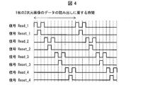
- FIG. 4 shows another example of a timing chart of the image capturing operation by the image capturing apparatus.
- the imaging apparatus interrupts reading of the data of the two-dimensional image and resets the active pixel sensor, and then performs reading again. This operation is performed in units of rows of the active pixel sensors, and is performed for the active pixel sensors in all rows within the time required for reading data of one two-dimensional image.
- Patent Document 1 and Non-Patent Document 1 disclose that resetting of an active pixel sensor and output reading are performed within a time (reading time) in which output reading is performed, within the reading time.
- a technique for controlling a RESET terminal so as not to perform the reset is not disclosed. Therefore, in an imaging apparatus including a plurality of active pixel sensors, when all active pixel sensors are reset at each readout time, readout is performed for the time required for resetting compared to the case where there are active pixel sensors that are not reset. There is a problem that the time is increased and the power consumption of the imaging apparatus is increased.
- an imaging apparatus including a conventional active pixel type radiographic imaging panel all the active pixel sensors are reset every time it takes to read data of one two-dimensional image. There were similar problems.
- the present invention has been made in order to solve the above-described problems, and its purpose is to realize radiation that has improved frame rate and reduced power consumption by shortening the total acquisition time of two-dimensional image data.
- An object is to provide an image pickup apparatus.
- a radiographic imaging device is a two-dimensionally arranged radiographic imaging device that acquires a two-dimensional image according to the dose of radiation that has been irradiated on a subject.
- the plurality of pixels and each of the plurality of pixels are provided, and when the radiation is incident on the plurality of pixels, a charge corresponding to the dose is accumulated for each of the pixels for at least two consecutive frames.
- the capacitor and at least one pixel of the plurality of pixels are accumulated from the pixel without initializing the at least one pixel in each of the first frame and the second frame constituting the two frames.
- a read control unit that reads out the first output and the second output corresponding to the charge.
- the present invention it is possible to improve the frame rate and suppress power consumption by not initializing at least one pixel in each of the continuous first frame and second frame.
- Embodiment 1 Hereinafter, embodiments of the present invention will be described in detail with reference to FIGS. 1 and 5 to 8.
- FIG. 5 is a circuit diagram showing the main part of the radiation image capturing apparatus 100.
- the radiographic image capturing apparatus 100 captures a moving image by continuously generating two-dimensional image data corresponding to the dose X of radiation that has been irradiated onto a subject.
- the radiographic imaging device 100 includes an imaging panel 20, a control unit 21, a read element control unit (read control unit) 22, a reset element control unit (read control unit) 23, a current / voltage conversion amplifier ( Hereinafter, an abbreviated “IV amplifier”) 24 and an image data generation unit (output generation unit) 25 are provided.
- an abbreviated “IV amplifier” 24 and an image data generation unit (output generation unit) 25 are provided.
- Imaging panel 20 is a flat plate-like substrate, in a plan view, n rows ⁇ n columns in total the n 2 active pixel (more pixels) 10 are arranged in a matrix.
- the number and arrangement of the active pixels 10 are not particularly limited as long as they are two-dimensionally arranged, but FIG. 2 illustrates an arrangement of 4 rows ⁇ 4 columns for ease of illustration.
- the control unit 21 controls the read element control unit 22, the reset element control unit 23, and the image data generation unit 25, and also performs overall control of the radiation image capturing apparatus 100.
- the read element control unit 22 sends the read signals Read_1 to Read_4 to the read element 3 for each row of active pixels 10 (one row is composed of four active pixels 10) (to be described later with reference to FIG. 1). Is output to the gate electrodes of the first and second output electrodes Iout_1 to Iout_4 by the read element 3 is controlled.
- the read signals Read_1 to Read_4 have a high level (High) period for reading execution and a low level (Low) period for reading interruption.
- the reset element control unit 23 controls the initialization of the active pixel 10 by the reset element 4 by outputting the reset signal Reset_all to the gate electrodes of all the reset elements 4 (described later with reference to FIG. 1).
- the reset signal Reset_all has a high level (High) period for executing initialization and a low level (Low) period for interrupting initialization.
- the IV amplifier 24 converts the output currents Iout_1 to Iout_4 output from the read element 3 into output voltages Vout_1 to Vout_4, and outputs them to the image data generation unit 25.
- the image data generation unit 25 generates 4 ⁇ 4 resolution two-dimensional image data proportional to the change amount ⁇ X of the radiation dose X incident on the active pixel 10 based on the input output voltages Vout_1 to Vout_4. . Data processing by the image data generation unit 25 will be described later.
- FIG. 1 is a circuit diagram showing the main part of the active pixel 10.
- the active pixel 10 converts the radiation dose X that has been irradiated onto the subject into an output current Iout that is used to generate two-dimensional image data, and outputs the output current Iout.
- the active pixel 10 includes a sensor element 1, an amplification element 2, a read element 3, and a reset element 4.
- TFT elements are used as the amplifying element 2, the read element 3, and the reset element 4.
- the sensor element 1 is an element that detects that the radiation that has been irradiated to the subject has entered the active pixel 10, and includes a capacitive element 1a that accumulates electric charges according to the dose X.
- the sensor element 1 may be, for example, a photodiode, and the capacitive element 1a may be configured by a capacitance between terminals of the sensor element 1, for example.
- a bias voltage Vsb is applied to the input terminal of the sensor element 1 from a bias power source (not shown), and the output terminal is connected to the gate electrode of the amplifying element 2 and the drain electrode of the reset element 4. Further, the sensor element 1 applies an electric signal corresponding to the electric charge accumulated in the capacitive element 1 a to the gate electrode of the amplifying element 2 in a state where the reset element 4 is off.
- the amplifying element 2 the voltage of the gate electrode (gate voltage) changes according to the electric charge accumulated in the capacitive element 1a. Then, the amplifying element 2 outputs the change in the gate voltage as an amplified current change between the drain and the source to the source electrode of the read element 3.
- a power source voltage Vd is applied to the source electrode of the amplifying element 2 from a power source (not shown) of the amplifying element 2, and the drain electrode is connected to the source electrode of the read element 3.
- the read element 3 reads the electric signal amplified by the amplifying element 2 as the output current Iout in accordance with the read signal Read output from the read element control unit 22 and outputs it to the IV amplifier 24.
- the read element 3 when the read signal Read input to the gate electrode of the read element 3 is High, the read element 3 outputs the output current Iout because the emitter and collector of the read element 3 are conductive. On the other hand, when the read signal Read is Low, the emitter and the collector are cut off. That is, the read element 3 functions as a switch element, and reading is executed when ON and reading is interrupted when OFF.
- the reset element 4 initializes the active pixel 10 in response to the reset signal Reset_all output from the reset element control unit 23.
- the reason for initializing the active pixel 10 is that if the electric charge is accumulated too much and the potential of the capacitive element 1a becomes too large, the output current Iout output from the amplifying element 2 is saturated, and consequently the output voltage Vout is saturated. . For this reason, by returning the potential to the initial potential Vb before the potential of the capacitive element 1a becomes too large, the amplifying element 2 can be operated at an appropriate signal amplification factor.
- the reset signal Reset_all input to the gate electrode of the reset element 4 is High
- the emitter and collector of the reset element 4 are electrically connected to connect the capacitive element 1a to the initial potential Vb.
- the reset signal Reset_all is Low
- the emitter and the collector are cut off. That is, the reset element 4 functions as a switch element, and initialization is performed when turned on, and initialization is suspended when turned off (that is, charge accumulation by the capacitive element 1a).
- FIG. 6 is a diagram illustrating a timing chart of an image capturing operation performed by the radiation image capturing apparatus 100.
- FIG. 7 is a graph showing the relationship between the dose X of radiation incident on the active pixel 10 and the output voltage Vout.
- the image capturing operation by the radiation image capturing apparatus 100 is composed of two phases of an initialization period and an image data generation period.
- the image data generation period is composed of three phases: a first readout period, a second readout period, and an additional period for signal accumulation.
- the additional period for signal accumulation is a period that is added as necessary to secure the signal accumulation time for obtaining the required signal strength. If the time length is zero, that is, the additional period is set. Sometimes not.
- the time length of the additional period for signal accumulation is assumed to be a subframe. Note that the additional period for signal accumulation also functions as a redundant period for ensuring the uniformity of the frame period.
- the elapsed time of the first readout period and each time length of the second readout period are one frame.
- one frame specifically refers to the time required to read the output voltages Vout_1 to Vout_4 from each column of the active pixels 10.
- the time length of the first readout period is the first frame
- the time length of the second readout period is the second frame.
- the active pixel 10 in the i-th row and j-th column read in the n-th High period of the read signal Read_i without being initialized.
- the output current is Iout (i, j, n)
- the output voltage is Vout (i, j, n).
- X (i, j, n) be the dose of radiation incident on the active pixel 10 in the i-th row and j-th column before the n-th readout.
- the reset element control unit 23 outputs the first High reset signal Reset_all from the output terminals connected to the gate electrodes of all the reset elements 4 before the start of the image data generation period. 4 is turned ON, and all the active pixels 10 are initialized.
- the initialization time required for initialization of the active pixel 10 (that is, the time length of the initialization period) is the capacitance of the capacitive element 1a, the resistance value of the line to which the initial potential Vb is applied, and the voltage source of the initial potential Vb. Determined based on impedance.
- every three image data generation periods required to generate three two-dimensional image data from a total of 16 active pixels 10 arranged in a 4 ⁇ 4 matrix are passed.
- All active pixels 10 are initialized. That is, in this embodiment, the initialization period for initializing all the active pixels 10 is the total time length of 4 frames (time length of a plurality of frames, see FIG. 6) and 3 subframes (see FIG. 6). It becomes. Then, the reset element control unit 23 initializes all the active pixels 10 at a time when four frames have elapsed.
- the initialization cycle of the active pixel 10 is not limited to the above case. That is, the purpose of the initialization is to prevent saturation of the output voltage Vout, and the saturation occurs when the capacitive element 1a is in a saturated state (a state where charge cannot be accumulated). Alternatively, the saturation occurs when the voltage applied to the gate electrode of the amplifying element 2 becomes too large and the output current Iout of the amplifying element 2 is saturated. Therefore, the time required until the amount of charge accumulated in the capacitor element 1a once initialized reaches a threshold value (for example, the amount of charge slightly smaller than the amount of charge at which the capacitor element 1a is saturated) is calculated in advance. By doing so, the initialization period may be determined. For example, assuming a maximum input of the dose X of the radiation incident on the active pixel 10 and determining in advance how long the threshold is to be reached when the maximum input continues, the initialization period (the number of frames) ) May be determined.
- the reset element control unit 23 initializes each of the active pixels 10 within the initialization period so that all the active pixels 10 are initialized at the end of the initialization period. That's fine.
- the initialization period must be defined as a time length of a plurality of frames or a total time length of a plurality of frames and a plurality of subframes.
- the operation of generating 4 ⁇ 4 resolution two-dimensional image data is started. That is, the first image data generation period starts. Specifically, the reset element control unit 23 outputs the first Low reset signal Reset_all from the output terminal to turn off all the reset elements 4. At the same time, the read element control unit 22 sequentially outputs the first High read signal Read_1, the read signal Read_2, and the read signal Read_3 from each output terminal connected to the gate electrode of the read element 3 for each row of the active pixels 10. The read signal Read_4 is output.
- output current Iout (i, 1, 1), output current Iout (i, 2, 1), The output current Iout (i, 3, 1) and the output current Iout (i, 4, 1) are read out through each read element 3.
- the four output currents Iout read out are output by the IV amplifier 24 as output voltage Vout (i, 1, 1), output voltage Vout (i, 2, 1), output voltage Vout (i, 3, 1), and output. Each of the voltages is converted into a voltage Vout (i, 4, 1) and output to the image data generation unit 25. When all of the four output voltages Vout (first output) are input to the image data generation unit 25, the first first readout period ends.
- the first second read period starts after the first first read period ends.
- the reset element control unit 23 and the read element control unit 22 perform the same signal output control as in the first readout period. Then, four outputs of the output voltage Vout (i, 1, 2), the output voltage Vout (i, 2, 2), the output voltage Vout (i, 3, 2), and the output voltage Vout (i, 4, 2).
- the voltage Vout (second output) is sequentially output to the image data generation unit 25.
- the image data generation unit 25 determines that the output voltage Vout read during the first first read period and the output voltage Vout read during the first second read period are 1 Two-dimensional image data is generated.
- Vout (i, j, 1) the output voltage of the active pixel 10 in the i-th row and j-th column read out during the first High period of the read signal Read_i
- Vout (i, j, 2) ⁇ Vout (i, j, 1) ⁇ ⁇ X (i, j, 2) ⁇ X ( i, j, 1) ⁇
- Vout (i, j, 2) ⁇ Vout (i, j, 1) ⁇ ⁇ X (i, j, 2) ⁇ X ( i, j, 1) ⁇ is established. Therefore, by calculating Vout (i, j, 2) ⁇ Vout (i, j, 1), the change in the dose X of the radiation incident on the active pixel 10 during the period from the first readout period to the second readout period. An amount ⁇ X is calculated.
- the read time of the output voltage Vout for each active pixel 10 that is, the high period of the read signal Read is sufficiently shorter than the incident time of radiation to the active pixel 10. Therefore, in each of the embodiments below, in the period for reading the output voltage Vout from the active pixel 10 in the i-th row and the j-th column during the first readout period and the second readout period (High period of the read signal Read_i).
- the dose X of the incident radiation and the output voltage Vout corresponding to the dose X are assumed to be constant.
- the image data generation unit 25 acquires one piece of 4 ⁇ 4 resolution two-dimensional image data
- the first second read period ends and the first image data generation period. Ends.
- the image data generation unit 25 acquires 4 ⁇ 4 resolution two-dimensional image data one by one in the same manner as described above.
- Vout (i, j, n) Vout (i, j, n)
- Vout (i, j, n + 1) ⁇ Vout (i, j, n) ⁇ ⁇ X (i, j, n + 1) ⁇ X ( i, j, n) ⁇
- the variation ⁇ X is calculated by calculating Vout (i, j, n + 1) ⁇ Vout (i, j, n).
- the image data generation unit 25 outputs the output voltage (second amplified output) Vout (i, j, n + 1) read by the read element control unit 22 and the output voltage (first amplified output) Vout (i, The difference ⁇ X (readout output corresponding to the radiation dose) is generated by obtaining the difference from j, n). Then, the image data generation unit 25 generates two-dimensional image data proportional to the change amount ⁇ X for each active pixel 10.
- the second readout period in the first image data generation period is the first readout period in the second image data generation period.
- the second readout period in the second image data generation period is the first readout period in the third image data generation period.
- FIG. 8 is a flowchart showing the processing.
- a specific active pixel 10 is taken as an example. It goes without saying that the same description applies to the other active pixels 10.
- the reset element control unit 23 outputs a high reset signal Reset_all before starting image capturing, and initializes the active pixel 10 (all other active pixels 10 are also initialized). (Step 100; imaging preparation step, hereinafter abbreviated as S100).
- the sensor element 1 After the imaging starts, the sensor element 1 accumulates charges corresponding to the dose X of the incident radiation in the capacitive element 1a when radiation irradiated on the subject enters the active pixel 10 (S101; charge accumulation step).
- the reset element control unit 23 determines whether or not the image data generation period has passed three times (S102; initialization execution determination step). If YES is determined in S102 (hereinafter abbreviated as Y), the reset element control unit 23 initializes the active pixel 10 (all other active pixels 10 are also initialized), and the process of S101 is performed again. The process proceeds (S103; initialization execution step).
- the reset element control unit 23 transmits a determination result to that effect to the read element control unit 22.
- the read element control unit 22 that has received the determination result outputs a high read signal Read (S104; read signal output step).
- the amplifying element 2 and the read element 3 are turned on. Then, the output voltage Vout corresponding to the charge accumulated in the capacitive element 1a is read out from the active pixel 10 via the IV amplifier 24 (S105; output reading step). The read output voltage Vout is output to the image data generation unit 25.
- the image data generation unit 25 determines whether or not the input output voltage Vout has been read during the second read period (S106; calculation execution determination step). When it is determined as S in S106, the image data generation unit 25 determines the difference between the output voltage Vout input during the second readout period and the output voltage Vout input during the first readout period stored in the memory. Based on this, a change amount ⁇ X of the dose X of the radiation incident on the active pixel 10 is calculated (S107; calculation execution step).
- the memory may be built in the image data generating unit 25 or may be provided outside.
- the image data generation unit 25 stores the input data of the output voltage Vout in the memory without executing the calculation of the change amount ⁇ X. And it transfers to the process of S101 again.
- the radiographic image capturing apparatus 100 determines whether or not an imaging end operation has been performed by the user (S108; imaging end determination step). This determination may be made, for example, by an imaging end determination unit (not shown) provided in the radiation image capturing apparatus 100. Further, for example, the operation input unit and the power switch unit (both not shown) similarly provided in the radiation image capturing apparatus 100 may be used.
- the radiation image capturing apparatus 100 ends the image capturing process. On the other hand, when it determines with N by S108, it transfers to the process of S101 again.
- the radiographic image capturing apparatus 100 does not initialize all the active pixels 10 in each of the first readout period and the second readout period, that is, each of the continuous first frame and second frame.
- the output current Vout corresponding to the first frame and the output current Vout corresponding to the second frame are read from the active pixel 10. Further, the read operation of the output current Vout between two consecutive frames is repeated within an initialization period composed of a plurality of frames. Therefore, the frame rate can be improved and the power consumption can be suppressed as compared with the case where all the active pixels 10 are initialized for each frame.
- the output terminal of the reset element control unit 23 is connected to the gate electrode of the read element 3 for each row of the active pixels 10, and reset signals Reset_1 ⁇ It is different from the radiographic image capturing apparatus 100 according to the first embodiment in that Reset_4 is output.
- the radiographic image capturing apparatus 200 is different from the radiographic image capturing apparatus 100 in that only four active pixels 10 constituting one row are initialized in one frame.
- FIG. 10 is a diagram illustrating a timing chart of an image capturing operation performed by the radiation image capturing apparatus 200.
- the image capturing operation by the radiation image capturing apparatus 200 is composed of one phase of the image data generation period as shown in FIG.
- the image data generation period is composed of two phases of a first initialization / readout period and a second initialization / readout period, and the time length of both periods is one frame. Further, the first initialization / readout period is the first frame, and the second initialization / readout period is the second frame.
- an additional period for signal accumulation is not set between the frames, it goes without saying that the additional period may be set.
- the read element control unit 22 sequentially outputs the first high read signal Read_1, read signal Read_2, read signal Read_3, and read signal Read_4 from each output terminal. At this time, the read element control unit 22 controls the signal output so that only the read signal Read_1 is interrupted for the High period.
- the reset element control unit 23 starts the initialization of each active pixel 10 in the first row when the first high period of the first read signal Read_1 is interrupted.
- Reset signal Reset_1 is output. That is, the fall of the first High period of the first read signal Read_1 is synchronized with the rise of the first High reset signal Reset_1.
- the read element control unit 22 controls the signal output so that the latter High period of the first read signal Read_1 is resumed. That is, the falling of the first High reset signal Reset_1 is synchronized with the rising of the latter High period of the first read signal Read_1.
- the active pixel 10 is initialized during the interruption period of reading the output voltage Vout.
- the initialization of the active pixel 10 is performed simultaneously. May be made.
- the output voltage read immediately before the initialization is Vout5 (1, j, 1), and the output read immediately after the initialization.
- the voltage is Vout1 (1, j, 1).
- the read output voltages are Vout4 (2, j, 1), Vout3 (3, j, 1), and Vout2 (4, j, 1), respectively. .
- the read output voltages Vout are output to the image data generation unit 25.
- the first first initialization / readout period ends.
- the first second initialization / readout period starts after the first first initialization / readout period ends. Specifically, the read element control unit 22 outputs each read signal Read for the second time so that only the read signal Read_2 is temporarily interrupted for the High period.
- the reset element control unit 23 outputs the second High reset signal Reset_2 so that each active pixel 10 in the second row is initialized after the high period of the second read signal Read_2 is interrupted. .
- the output voltage read immediately before initialization is Vout5 (2, j, 2)
- the output voltage read immediately after initialization is Vout1 ( 2, j, 2).
- the read output voltages are Vout2 (1, j, 2), Vout4 (3, j, 2), and Vout3 (4, j, 2), respectively. .
- Each read output voltage Vout is output to the image data generation unit 25.
- the image data generation unit 25 outputs the output voltage Vout read during the first first initialization / readout period and the output voltage Vout read during the first second initialization / readout period. Based on the above, data for one two-dimensional image is generated.
- the output voltage of the active pixel 10 in the first row and jth column read out during the first second High period of the read signal Read_1 is Vout1 (1, j, 1)
- Vout2 (1, j, 2) ⁇ Vout1 (1, j, 1) The relationship of ⁇ ⁇ X (1, j, 2) ⁇ X (1, j, 1) ⁇ is established. Therefore, the image data generation unit 25 calculates Vout2 (1, j, 2) ⁇ Vout1 (1, j, 1) for each active pixel 10 in the first row, so that the first initialization / readout period is calculated.
- the change amount ⁇ X of the radiation dose X incident on each active pixel 10 is calculated.
- the image data generating unit 25 acquires one piece of 4 ⁇ 4 resolution two-dimensional image data
- the first second initialization / readout period ends and the first image The data generation period ends.
- the image data generation unit 25 acquires 4 ⁇ 4 resolution two-dimensional image data one by one in the same manner as described above.
- the second initialization / readout period in the nth image data generation period is the first initialization / readout period in the (n + 1) th image data generation period.
- the reset element control unit 23 initializes the active pixels 10 in different rows for each frame. Since at least one of the active pixels 10 is initialized for each frame, it is not necessary to provide a period for pausing the generation of two-dimensional image data in order to initialize all the active pixels 10 at once. Therefore, data of a plurality of two-dimensional images can be generated continuously without interruption, and the frame period can be kept constant without providing an additional period for signal accumulation as in the first embodiment, that is, a redundant period. Can be secured.
- the actual number (i ⁇ j) of the active pixels 10 included in the radiographic image capturing apparatus according to the present invention is much larger than 4 ⁇ 4, actually, the plurality of frames constituting the initialization cycle are actually included.
- active pixels 10 in a plurality of rows are initialized.
- the image data generation unit 25 calculates an approximate function indicating the relationship between the dose X of the radiation incident on the active pixel 10 and the output voltage Vout read from the active pixel 10. It is different from the radiation image capturing apparatuses 100 and 200 according to the first and second embodiments in that the amount of change ⁇ X of the radiation dose X is calculated.
- the configuration of the main part of the radiographic image capturing apparatus 300 is the same as the configuration of the main part of the radiographic image capturing apparatus 100 according to the first embodiment.
- the signal output control by the read element control unit 22 and the reset element control unit 23 provided in the radiographic image capturing apparatus 300 is also the same as that of the radiographic image capturing apparatus 100 (see FIG. 5).
- the configuration of the main part of the radiographic image capturing apparatus 300 may be the same as that of the radiographic image capturing apparatus 200 according to the second embodiment, for example.
- FIG. 11 is a graph showing the relationship between the dose X of radiation incident on the active pixel 10 included in the radiation image capturing apparatus 300 and the output voltage Vout read from the active pixel 10.
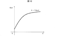
- FIG. 12 is a graph showing the relationship between the radiation dose X and the output voltage Vout as an approximate function.
- the imaging operation is repeated without initializing the active pixel 10, the amount of charge accumulated in the capacitive element 1 a increases, so that the change width of the gate voltage of the amplifying element 2 increases correspondingly. Sex appears more prominently.
- the surface of the imaging panel 20 where the active pixels 10 are arranged is continuously irradiated with a uniform dose of radiation.
- the output voltage immediately after initialization is V 0, and then V 1, V 2, V 3, V 4,..., VN, every fixed frame (may be every frame or every few frames).
- the output voltage Vout is read out. Based on the data of the read output voltage Vout, as shown in FIG. 11, the relationship between the radiation dose X and the output voltage Vout corresponding to the dose X is graphed.
- X1, X2, X3, X4,..., XN represent the radiation dose X incident on the specific active pixel 10.
- Vout the output voltage
- X is expressed as a function of Vout, as shown in the graph of FIG.
- an approximate function deriving unit (not shown) may be provided inside or outside the image data generating unit 25 so that the radiation is automatically derived when the radiation enters the active pixel 10.
- the output voltage of the active pixel 10 in the i-th row and j-th column read during the n-th High period of the read signal Read_i is Vout (i, j, n), and the (n + 1) -th High period of the read signal Read_i.
- control blocks (particularly the read element control unit 22 and the reset element control unit 23) of the radiation image capturing apparatus 100 may be realized by a logic circuit (hardware) formed in an integrated circuit (IC chip) or the like, or a CPU It may be realized by software using (Central Processing Unit).
- the radiographic imaging apparatus 100 includes a CPU that executes instructions of a program that is software that implements each function, and a ROM (Read Only Memory) in which the program and various data are recorded so as to be readable by the computer (or CPU). ) Or a storage device (these are referred to as “recording media”), a RAM (Random Access Memory) that expands the program, and the like. And the objective of this invention is achieved when a computer (or CPU) reads the said program from the said recording medium and runs it.
- a “non-temporary tangible medium” such as a tape, a disk, a card, a semiconductor memory, a programmable logic circuit, or the like can be used.
- the program may be supplied to the computer via an arbitrary transmission medium (such as a communication network or a broadcast wave) that can transmit the program.
- a transmission medium such as a communication network or a broadcast wave
- the present invention can also be realized in the form of a data signal embedded in a carrier wave in which the program is embodied by electronic transmission.
- a radiographic image capturing apparatus (100, 200, 300) according to aspect 1 of the present invention is a radiographic image capturing apparatus that acquires a two-dimensional image corresponding to a dose (X) of radiation that has been irradiated on a subject.
- a plurality of arranged pixels active pixels 10) and each of the plurality of pixels, and the radiation is incident on the plurality of pixels, so that the dose is set for each of the pixels between at least two consecutive frames.
- the at least one pixel is initialized in each of the first frame and the second frame constituting the two frames with respect to the capacitive element (1a) that accumulates the corresponding charge and at least one of the plurality of pixels.
- the first output (output voltage Vout) and the second output (output voltage Vout) corresponding to the accumulated charges are read from the pixel. Includes a to read control unit (read-element control portion 22, the reset element control unit 23), the.
- the read control unit does not initialize at least one pixel of a plurality of pixels arranged two-dimensionally in each of the first frame and the second frame configuring two consecutive frames.
- the first output and the second output corresponding to the charge accumulated in the capacitor are read from the pixel.
- “one frame” refers to the time required to read data of one two-dimensional image from a plurality of pixels arranged two-dimensionally.
- the total acquisition time of two-dimensional image data can be shortened, and the power consumption required for the initialization of the at least one pixel can be reduced. Can be reduced.
- the radiographic image capturing apparatus (100, 200, 300) according to aspect 2 of the present invention is the aspect 1, wherein the initialization cycle for initializing each of the plurality of pixels (active pixels 10) is a time of a plurality of frames.
- the read control unit (reset element control unit 23) sets each of the plurality of pixels so that all of the plurality of pixels are initialized at the end of the initialization period. You may initialize within the said initialization period.
- the amount of charge accumulated in the capacitor element of the pixel increases according to the number of repetitions of the reading I will do it.
- the capacitive element becomes saturated so that it can no longer accumulate charge, and the first output read after reaching the predetermined amount.
- the second output is saturated. Therefore, after the predetermined amount is reached, the read first output and second output do not correspond to the radiation dose that has passed through the subject.
- the radiographic imaging device can read out the first output and the second output corresponding to the radiation dose while shortening the time of one frame.
- the radiographic imaging device (100, 200) according to aspect 3 of the present invention is the above-described aspect 1 or 2, wherein the plurality of pixels (active pixels 10) amplify the first output or the second output.
- the read control unit (read element control unit 22) includes a second amplified output (output voltage Vout) obtained by amplifying the second output from each of the plurality of pixels, and the first output.
- the first amplified output (output voltage Vout) is amplified and the difference between the second amplified output read by the read control unit and the first amplified output is obtained, whereby the radiation dose (X ) May further include an output generation unit (image data generation unit 25) that generates a read output (change amount ⁇ X).
- the plurality of pixels further include the amplifying element that amplifies the first output or the second output, and the read control unit outputs the second output obtained by amplifying the second output from each of the plurality of pixels.
- the amplified output and the first amplified output obtained by amplifying the first output are read out. Therefore, the radiographic image capturing apparatus can more reliably read the output from each of the plurality of pixels as the first amplification output and the second amplification output even when noise or the like occurs in the read control unit. it can.
- the radiographic image device generates a readout output corresponding to the dose of radiation that has been irradiated on the subject by obtaining a difference between the second amplified output and the first amplified output.
- the radiographic image capturing apparatus reads out the first amplified output even when the pixel to be read out is not initialized in the two frames corresponding to the readout of the first amplified output and the second amplified output.
- the dose of the radiation incident on the pixel from the time point to the time point when the second amplified output is read can be obtained with a value close to the actual measurement using the read output.
- the image data of each frame can be obtained by subtracting the output read immediately after initialization from the output read after the charge accumulation period. Since the noise accumulated in the pixels at the time of initialization is removed by such a readout operation using double sampling, the radiographic imaging device can acquire image data with little noise.
- the output generation unit (image data generation unit 25) is configured so that the initialized specific pixel (active The relationship between the dose (X) of the radiation continuously irradiated to the pixel 10) and the output (output voltage Vout) corresponding to the electric charge accumulated in the capacitive element (1a) according to the dose is shown.
- the second correction output (f (Vout)) obtained by substituting the second amplified output (output voltage Vout) into the approximate function and the approximate function
- the readout output (change amount ⁇ X) may be generated by obtaining a difference from the first correction output (f (Vout)) obtained by substituting the first amplified output (output voltage Vout) for. .
- the output generation unit generates a dose of radiation continuously applied to the initialized specific pixel and an output corresponding to the charge accumulated in the capacitive element according to the dose.
- the first correction output and the second correction output are: The value is closer to the actual measured value of the radiation dose that has passed through the subject. Therefore, the output generation unit can generate the read output closer to the actual measurement value as compared with the case of obtaining the difference between the second amplification output and the first amplification output.
- the output generation unit corresponds to the approximation corresponding to each of the plurality of pixels (active pixels 10).
- the relationship between the dose of radiation incident on the pixel and the output from the pixel corresponding to the dose is due to the difference in the characteristics of the elements provided in the pixel, the difference in the arrangement location of the pixel on the imaging panel, etc.
- Each of the plurality of pixels is different.
- the output generation unit generates a read output corresponding to each of the plurality of pixels by using the above approximate function corresponding to each of the plurality of pixels. Therefore, for example, the output generation unit generates the read outputs closer to the measured values of the corresponding pixels as compared with a case where an approximate function corresponding to a specific pixel is used as an approximate function of another pixel. can do.
- a radiographic image capturing method is a radiographic image capturing method for acquiring a two-dimensional image corresponding to a dose (X) of radiation that has been irradiated on a subject.
- a charge accumulating step (S101) for accumulating charges corresponding to the dose for each pixel between at least two consecutive frames when the radiation enters the active pixel 10); and at least one pixel of the plurality of pixels In each of the first frame and the second frame constituting the two frames, the first output (output voltage Vout) corresponding to the accumulated charge is output from the pixel without initializing the at least one pixel.
- an output reading step (S105) for reading out the second output (output voltage Vout).
- the radiographic imaging device (100, 200, 300) according to each aspect of the present invention may be realized by a computer.
- the computer is provided as each unit (limited to software elements) included in the radiographic imaging device.
- a program that causes the radiographic imaging apparatus to be realized by a computer by operating the program and a computer-readable recording medium that records the program also fall within the scope of the present invention.
Landscapes
- Health & Medical Sciences (AREA)
- Life Sciences & Earth Sciences (AREA)
- Engineering & Computer Science (AREA)
- High Energy & Nuclear Physics (AREA)
- Medical Informatics (AREA)
- Physics & Mathematics (AREA)
- Molecular Biology (AREA)
- Nuclear Medicine, Radiotherapy & Molecular Imaging (AREA)
- General Health & Medical Sciences (AREA)
- Spectroscopy & Molecular Physics (AREA)
- Biophysics (AREA)
- Veterinary Medicine (AREA)
- Public Health (AREA)
- Optics & Photonics (AREA)
- Pathology (AREA)
- Radiology & Medical Imaging (AREA)
- Biomedical Technology (AREA)
- Heart & Thoracic Surgery (AREA)
- Surgery (AREA)
- Animal Behavior & Ethology (AREA)
- General Physics & Mathematics (AREA)
- Multimedia (AREA)
- Signal Processing (AREA)
- Computer Vision & Pattern Recognition (AREA)
- Measurement Of Radiation (AREA)
- Transforming Light Signals Into Electric Signals (AREA)
- Apparatus For Radiation Diagnosis (AREA)
Abstract
フレームレートの向上および消費電力の抑制を図る。放射線画像撮像装置(100)は、複数の画素と、放射線の線量(X)に応じた電荷を蓄積する容量素子(1a)と、2フレーム以上初期化されない少なくとも1つの画素(アクティブピクセル10)から、電荷に応じた出力(出力電圧Vout)を読み出すリード制御部(リード素子制御部22、リセット素子制御部23)と、を備える。
Description
本発明は、放射線、特にX線を用いた画像撮像装置に関する。
従来から、被写体に対する照射を経た放射線、特にX線の線量に応じた電荷(電気信号)を出力するセンサ素子を、2次元的に配置した放射線画像撮像用パネルの開発が進められている。上記センサ素子は、基板(パネル)上に2次元マトリックス状に配置された複数の画素毎に備えられている。この放射線画像撮像用パネルにおいては、各画素に備えられた容量素子に上記電荷が蓄積され、蓄積された電荷に対応した出力を各画素から読み出す制御は、薄膜トランジスタ(TFT;Thin Film Transistor)素子によって行われる。
特に、近年においては、蓄積された電荷に対応した出力を読み出すための回路等に発生する雑音の影響を低減する要請が高まってきた。この要請を受けて、画素に増幅素子としてのTFT素子をさらに設けて、上記出力を増幅して上記回路に伝送するアクティブピクセル型の放射線画像撮像用パネル、および該パネルを備えた撮像装置の開発が活発化している。
例えば、特許文献1および非特許文献1には、AMP(出力増幅)用のTFTと、READ(出力読み出し)用のTFTと、RESET(アクティブピクセルセンサのリセット)用のTFTとを備えたアクティブピクセルセンサが開示されている。ここで、アクティブピクセルセンサのリセットとは、AMP用のTFTのドレインソース間の電流があらかじめ定められた値となるように、当該AMP用のTFTのゲート電圧を、設定された初期電位に戻すことを指す。また、従来のアクティブピクセルセンサとしては、上記3つのTFTと上記センサ素子とを図1に示すように接続したものがある。また、従来のアクティブピクセル型の放射線画像撮像用パネルとしては、図2に示すような、基板上に図1のアクティブピクセルセンサが2次元マトリックス状に配置され、Reset信号生成回路、Read信号生成回路、制御回路および電流/電圧変換アンプを備えたものがある。なお、図2では、説明の便宜上、アクティブピクセルセンサの数を4×4の計16個としている。Reset信号生成回路は、アクティブピクセルセンサをリセットするための信号Reset_1’~Reset_4 ’を生成し、出力する。Read信号生成回路は、各アクティブピクセルセンサから出力電流Iout_1’~Iout_4’を読み出すための信号Read_1’~Read_4 ’を生成し、出力する。
次に、図2に示す撮像用パネルを備えた撮像装置による画像撮像動作のタイミングチャートの一例を図3に示す。図3に示すように、この撮像装置は、1枚の2次元画像のデータの読み出しに要する時間毎に全てのアクティブピクセルセンサの容量素子をリセットする。また、上記撮像装置による画像撮像動作のタイミングチャートの他の例を図4に示す。図4に示すように、この撮像装置は、2次元画像のデータの読み出しを中断してアクティブピクセルセンサをリセットした後、再び読み出しを行う。この動作は、アクティブピクセルセンサの行単位で行われ、1枚の2次元画像のデータの読み出しに要する時間内に全ての行のアクティブピクセルセンサについて行われる。
Taghibakhsh, F.; Karim, K.S., "Two-Transistor Active Pixel Sensor for High Resolution Large Area Digital X-ray Imaging," IEEE International Electron Devices Meeting 2007, pp.1011, 1014, 10-12, Dec. 2007
しかしながら、特許文献1および非特許文献1には、出力読み出しが行われる時間(読み出し時間)内にアクティブピクセルセンサのリセットおよび出力読み出しが行われることについては開示されているものの、当該読み出し時間内に上記リセットを行わないようにRESET用の端子を制御する技術については開示されていない。したがって、上記アクティブピクセルセンサを複数備えた撮像装置において、読み出し時間毎に全てのアクティブピクセルセンサがリセットされる場合、リセットされないアクティブピクセルセンサが存在する場合と比較して、リセットに要する時間分だけ読み出し時間が長くなり、撮像装置の消費電力も増加するという問題点があった。また、従来のアクティブピクセル型の放射線画像撮像用パネルを備えた撮像装置においても、1枚の2次元画像のデータの読み出しに要する時間毎に全てのアクティブピクセルセンサがリセットされることから、上記と同様の問題点があった。
本発明は、上記の問題点を解決するためになされたものであり、その目的は、2次元画像のデータの総取得時間の短縮化による、フレームレートの向上および消費電力の抑制を実現した放射線画像撮像装置を提供することにある。
上記の課題を解決するために、本発明の一態様に係る放射線画像撮像装置は、被写体に対する照射を経た放射線の線量に応じた2次元画像を取得する放射線画像撮像装置において、2次元的に配された複数の画素と、上記複数の画素の各々に備えられ、上記複数の画素に上記放射線が入射することにより、連続する少なくとも2フレーム間で上記画素ごとに上記線量に応じた電荷を蓄積する容量素子と、上記複数の画素の少なくとも1つの画素について、上記2フレームを構成する第1フレームおよび第2フレームの各々において、上記少なくとも1つの画素を初期化せずに、当該画素から、蓄積された上記電荷に対応した第1出力および第2出力を読み出すリード制御部と、を備える。
本発明の一態様によれば、連続する第1フレームおよび第2フレームの各々において、少なくとも1つの画素を初期化しないことにより、フレームレートの向上および消費電力の抑制を実現することができる。
〔実施形態1〕
以下、本発明の実施の形態について、図1および図5~図8を参照しながら、詳細に説明する。
以下、本発明の実施の形態について、図1および図5~図8を参照しながら、詳細に説明する。
<放射線画像撮像装置の構成>
まず、放射線画像撮像装置100の主要な構成について説明する。図5は、放射線画像撮像装置100の主要部を示す回路図である。放射線画像撮像装置100は、被写体に対する照射を経た放射線の線量Xに応じた2次元画像データを連続的に生成することにより、動画撮像を行うものである。図5に示すように、放射線画像撮像装置100は、撮像パネル20、制御部21、リード素子制御部(リード制御部)22、リセット素子制御部(リード制御部)23、電流/電圧変換アンプ(以下、「IVアンプ」と略記する)24および画像データ生成部(出力生成部)25を備えている。
まず、放射線画像撮像装置100の主要な構成について説明する。図5は、放射線画像撮像装置100の主要部を示す回路図である。放射線画像撮像装置100は、被写体に対する照射を経た放射線の線量Xに応じた2次元画像データを連続的に生成することにより、動画撮像を行うものである。図5に示すように、放射線画像撮像装置100は、撮像パネル20、制御部21、リード素子制御部(リード制御部)22、リセット素子制御部(リード制御部)23、電流/電圧変換アンプ(以下、「IVアンプ」と略記する)24および画像データ生成部(出力生成部)25を備えている。
撮像パネル20は平板状の基材であり、平面視において、n行×n列の合計n2個のアクティブピクセル(複数の画素)10がマトリックス状に配置されている。なお、アクティブピクセル10の個数および配置については、2次元的に配置されている限り特に限定されないが、図2では、図示を簡単にするため4行×4列の配列を例示している。
制御部21は、リード素子制御部22、リセット素子制御部23および画像データ生成部25の制御を行うとともに、放射線画像撮像装置100の統括的な制御も行う。
リード素子制御部22は、リード信号Read_1~Read_4を、アクティブピクセル10の行(4個のアクティブピクセル10で1つの行が構成される)毎のリード素子3(図1を参照して後述する)のゲート電極に出力することにより、リード素子3による出力電流Iout_1~Iout_4の読み出しを制御する。リード信号Read_1~Read_4は、読み出し実行用のハイレベル(High)の期間および読み出し中断用のローレベル(Low)の期間を有する。
リセット素子制御部23は、リセット信号Reset_allを、全てのリセット素子4(図1を参照して後述する)のゲート電極に出力することにより、リセット素子4によるアクティブピクセル10の初期化を制御する。リセット信号Reset_allは、初期化実行用のハイレベル(High)の期間および初期化中断用のローレベル(Low)の期間を有する。
IVアンプ24は、リード素子3から出力された出力電流Iout_1~Iout_4を出力電圧Vout_1~Vout_4に変換して、画像データ生成部25に出力する。
画像データ生成部25は、入力された出力電圧Vout_1~Vout_4に基づいて、アクティブピクセル10に入射した放射線の線量Xの変化量ΔXに比例する、4×4解像度の2次元画像のデータを生成する。なお、画像データ生成部25によるデータ処理については後述する。
なお、容量素子1a、リード素子3、リセット素子4、アクティブピクセル10およびアクティブピクセル10の初期化の詳細については、以下に説明する。
<アクティブピクセルの構成>
次に、アクティブピクセル10の主要な構成について説明する。図1は、アクティブピクセル10の主要部を示す回路図である。アクティブピクセル10は、被写体に対する照射を経た放射線の線量Xを、2次元画像のデータ生成に用いられる出力電流Ioutに変換して出力する。図1に示すように、アクティブピクセル10は、センサ素子1、増幅素子2、リード素子3およびリセット素子4を備えている。
<アクティブピクセルの構成>
次に、アクティブピクセル10の主要な構成について説明する。図1は、アクティブピクセル10の主要部を示す回路図である。アクティブピクセル10は、被写体に対する照射を経た放射線の線量Xを、2次元画像のデータ生成に用いられる出力電流Ioutに変換して出力する。図1に示すように、アクティブピクセル10は、センサ素子1、増幅素子2、リード素子3およびリセット素子4を備えている。
なお、本実施形態以下の各実施形態では、増幅素子2、リード素子3およびリセット素子4として、TFT素子が用いられているものとして説明する。
センサ素子1は、被写体に対する照射を経た放射線がアクティブピクセル10に入射したことを検知する素子であり、当該線量Xに応じた電荷を蓄積する容量素子1aを内蔵している。センサ素子1は、例えばフォトダイオードであってもよく、容量素子1aは、例えばセンサ素子1の端子間容量で構成されてもよい。センサ素子1の入力端にはバイアス電源(図示せず)からバイアス電圧Vsbが印加され、出力端は増幅素子2のゲート電極およびリセット素子4のドレイン電極に接続されている。また、センサ素子1は、リセット素子4がオフの状態において、容量素子1aに蓄積された電荷に対応した電気信号を増幅素子2のゲート電極に印加する。
増幅素子2では、容量素子1aに蓄積される電荷に応じてゲート電極の電圧(ゲート電圧)が変化する。そして、増幅素子2は、ゲート電圧の変化をドレインソース間の増幅された電流変化として、リード素子3のソース電極に出力する。増幅素子2のソース電極には、当該増幅素子2の電源(図示せず)から電源電圧Vdが印加され、ドレイン電極はリード素子3のソース電極に接続されている。
リード素子3は、リード素子制御部22から出力されるリード信号Readに応じて、増幅素子2によって増幅された電気信号を出力電流Ioutとして読み出し、IVアンプ24に出力する。
具体的には、リード素子3のゲート電極に入力されたリード信号ReadがHighの場合、リード素子3のエミッタとコレクタとが導通するので、リード素子3は出力電流Ioutを出力する。一方、リード信号ReadがLowの場合、エミッタとコレクタとは遮断状態となる。すなわち、リード素子3はスイッチ素子として機能し、ONで読み出し実行、OFFで読み出し中断となる。
リセット素子4は、リセット素子制御部23から出力されるリセット信号Reset_allに応じて、アクティブピクセル10を初期化する。ここで、アクティブピクセル10の初期化とは、容量素子1aの電位を、増幅素子2のゲートソース間の電圧が所定の閾値を少し超えるような初期電位Vbに戻すことを指す。初期電位Vbは、例えば、増幅素子2がN型TFT素子で所定の閾値が2Vであれば、Vb=3V程度に設定する。
アクティブピクセル10を初期化するのは、電荷が蓄積しすぎて容量素子1aの電位が大きくなりすぎると増幅素子2が出力する出力電流Ioutが飽和し、ひいては、出力電圧Voutが飽和するからである。このため、容量素子1aの電位が大きくなりすぎる前に当該電位を初期電位Vbに戻すことにより、増幅素子2を適切な信号増幅率で動作させることができる。
具体的には、リセット素子4のゲート電極に入力されたリセット信号Reset_allがHighの場合、リセット素子4のエミッタとコレクタとが導通して容量素子1aを初期電位Vbに接続する。一方、リセット信号Reset_allがLowの場合、エミッタとコレクタとは遮断状態となる。すなわち、リセット素子4はスイッチ素子として機能し、ONで初期化実行、OFFで初期化中断(すなわち、容量素子1aによる電荷蓄積)となる。
<放射線画像撮像装置による画像撮像動作>
次に、図6および図7を用いて、放射線画像撮像装置100による画像撮像動作について説明する。図6は、放射線画像撮像装置100による画像撮像動作のタイミングチャートを示す図である。図7は、アクティブピクセル10に入射した放射線の線量Xと出力電圧Voutとの関係を示すグラフである。
次に、図6および図7を用いて、放射線画像撮像装置100による画像撮像動作について説明する。図6は、放射線画像撮像装置100による画像撮像動作のタイミングチャートを示す図である。図7は、アクティブピクセル10に入射した放射線の線量Xと出力電圧Voutとの関係を示すグラフである。
放射線画像撮像装置100による画像撮像動作は、図6に示すように、初期化期間と画像データ生成期間との2フェーズで構成される。また、画像データ生成期間は、第1読み出し期間、第2読み出し期間および信号蓄積のための追加期間の3フェーズで構成される。
信号蓄積のための追加期間は、必要な信号強度を得るための信号蓄積時間を確保するために必要に応じて追加される期間であり、その時間長がゼロの場合、すなわち当該追加期間を設定しない場合もある。また、信号蓄積のための追加期間の時間長をサブフレームとする。なお、信号蓄積のための追加期間は、フレーム周期の一定性を確保するための冗長期間としても機能する。
さらに、第1読み出し期間の経過時間および第2読み出し期間の各時間長を1フレームとする。ここで、1フレームとは、具体的には、アクティブピクセル10の各列から出力電圧Vout_1~Vout_4を読み出すのに要する時間を指す。第1読み出し期間の時間長を第1フレーム、第2読み出し期間の時間長を第2フレームとする。
なお、以下の説明において、アクティブピクセル10を最初に初期化した後は、初期化しない状態でリード信号Read_iの第n回目のHigh期間に読み出された第i行第j列のアクティブピクセル10の出力電流をIout(i、j、n)、出力電圧をVout(i、j、n)とする。また、第n回目の読み出し時までに第i行第j列のアクティブピクセル10に入射した放射線の線量をX(i、j、n)とする。
(初期化期間)
まず、リセット素子制御部23は、画像データ生成期間の開始前に、全てのリセット素子4のゲート電極に接続された出力端子から第1回目のHighのリセット信号Reset_allを出力して全てのリセット素子4をONにし、全てのアクティブピクセル10を初期化する。ここで、アクティブピクセル10の初期化に要する初期化時間(すなわち、初期化期間の時間長)は、容量素子1aの容量、初期電位Vbを印加させるラインの抵抗値および初期電位Vbの電圧源のインピーダンスに基づいて決定される。
まず、リセット素子制御部23は、画像データ生成期間の開始前に、全てのリセット素子4のゲート電極に接続された出力端子から第1回目のHighのリセット信号Reset_allを出力して全てのリセット素子4をONにし、全てのアクティブピクセル10を初期化する。ここで、アクティブピクセル10の初期化に要する初期化時間(すなわち、初期化期間の時間長)は、容量素子1aの容量、初期電位Vbを印加させるラインの抵抗値および初期電位Vbの電圧源のインピーダンスに基づいて決定される。
このような制御を行うことで、画像データ生成期間の開始後すぐにアクティブピクセル10を初期化することなく、スムーズに、4×4解像度の2次元画像のデータを複数フレームにわたって連続生成することができる。
本実施形態では、4×4のマトリックス状に配置された計16個のアクティブピクセル10から3枚の2次元画像のデータを生成するのに必要な3回分の画像データ生成期間が経過する毎に、全てのアクティブピクセル10が初期化される。すなわち、本実施形態では、全てのアクティブピクセル10の各々を初期化する初期化周期が、4フレーム(複数フレームの時間長、図6参照)と3サブフレーム(図6参照)との合計時間長となる。そして、リセット素子制御部23は、4フレーム経過時点で全てのアクティブピクセル10を一括して初期化する。
但し、アクティブピクセル10の初期化周期は上記場合に限定されない。すなわち、上記初期化の目的が出力電圧Voutの飽和を防ぐことにあり、当該飽和は容量素子1aが飽和状態(電荷を蓄積できなくなる状態)になることによって生じる。あるいは、当該飽和は、増幅素子2のゲート電極に印加される電圧が大きくなりすぎて増幅素子2の出力電流Ioutが飽和することによって生じる。したがって、一旦初期化された容量素子1aに蓄積された電荷の量が閾値(例えば、容量素子1aが飽和状態になる電荷の量よりも若干少ない電荷の量)になるまでに要する時間をあらかじめ算出することで、初期化周期を決定すればよい。例えば、アクティブピクセル10に入射する放射線の線量Xの最大入力を想定し、当該最大入力が持続した場合にどの程度の時間で上記閾値になるかをあらかじめ求めた上で、初期化周期(フレーム数)を決定してもよい。
また、本実施形態のように初期化周期毎に全てのアクティブピクセル10を一括して初期化する必要はなく、例えば、1フレーム毎に1行ないし複数行のアクティブピクセル10を順次初期化してもよい(実施形態2参照)。また、換言すれば、リセット素子制御部23は、初期化周期の終わりに全てのアクティブピクセル10が初期化されているように、当該全てのアクティブピクセル10の各々を初期化周期内で初期化すればよい。
なお、フレームレートの向上という本発明の目的を達成するためには、初期化周期は、複数フレームの時間長、あるいは複数フレームと複数サブフレームとの合計時間長として定められなければならない。
(画像データ生成期間)
全てのアクティブピクセル10の初期化が終了した後、4×4解像度の2次元画像のデータの生成動作が開始される。すなわち、第1回目の画像データ生成期間が開始する。具体的には、リセット素子制御部23は、出力端子から第1回目のLowのリセット信号Reset_allを出力して全てのリセット素子4をOFFにする。同時に、リード素子制御部22は、アクティブピクセル10の行毎のリード素子3のゲート電極に接続された各出力端子から、順次、第1回目のHighのリード信号Read_1、リード信号Read_2、リード信号Read_3、リード信号Read_4を出力する。
全てのアクティブピクセル10の初期化が終了した後、4×4解像度の2次元画像のデータの生成動作が開始される。すなわち、第1回目の画像データ生成期間が開始する。具体的には、リセット素子制御部23は、出力端子から第1回目のLowのリセット信号Reset_allを出力して全てのリセット素子4をOFFにする。同時に、リード素子制御部22は、アクティブピクセル10の行毎のリード素子3のゲート電極に接続された各出力端子から、順次、第1回目のHighのリード信号Read_1、リード信号Read_2、リード信号Read_3、リード信号Read_4を出力する。
そして、アクティブピクセル10の列(4個のアクティブピクセル10で1つの列が構成される)毎に、順次、出力電流Iout(i、1、1)、出力電流Iout(i、2、1)、出力電流Iout(i、3、1)、出力電流Iout(i、4、1)が、各リード素子3を介して読み出される。
読み出された4個の出力電流Ioutは、IVアンプ24によって出力電圧Vout(i、1、1)、出力電圧Vout(i、2、1)、出力電圧Vout(i、3、1)、出力電圧Vout(i、4、1)にそれぞれ変換されて画像データ生成部25に出力される。上記4個の出力電圧Vout(第1出力)が画像データ生成部25に全て入力されると、第1回目の第1読み出し期間が終了する。
第1回目の第1読み出し期間の終了後、第1回目の第2読み出し期間が開始する。第2読み出し期間においても、リセット素子制御部23およびリード素子制御部22によって第1読み出し期間と同様の信号出力制御が行われる。そして、出力電圧Vout(i、1、2)、出力電圧Vout(i、2、2)、出力電圧Vout(i、3、2)、出力電圧Vout(i、4、2)の4個の出力電圧Vout(第2出力)が順次、画像データ生成部25に出力される。
次に、画像データ生成部25は、第1回目の第1読み出し期間に読み出された出力電圧Voutと、第1回目の第2読み出し期間に読み出された出力電圧Voutとに基づいて、1枚の2次元画像のデータを生成する。
具体的には、画像データ生成部25は、アクティブピクセル10に入射した放射線の線量Xの変化量ΔXと当該線量Xに対応する出力電圧Voutの変化量ΔVとが、図7に示すような比例関係(ΔV=α・ΔX、比例定数;α)にあると仮定して、変化量ΔXを計算する。そして、画像データ生成部25は、算出された変化量ΔXに比例する2次元画像のデータをアクティブピクセル10毎に生成し、4×4解像度の2次元画像のデータを1枚取得する。
すなわち、リード信号Read_iの第1回目のHigh期間に読み出された第i行第j列のアクティブピクセル10の出力電圧をVout(i、j、1)、リード信号Read_iの第2回目のHigh期間に読み出された出力電圧をVout(i、j、2)とすると、Vout(i、j、2)-Vout(i、j、1)=α{X(i、j、2)-X(i、j、1)}の関係が成立する。したがって、Vout(i、j、2)-Vout(i、j、1)を計算することで、第1読み出し期間から第2読み出し期間までの間にアクティブピクセル10に入射した放射線の線量Xの変化量ΔXが算出される。
なお、アクティブピクセル10毎の出力電圧Voutの読み出し時間、すなわちリード信号ReadのHigh期間は、放射線のアクティブピクセル10への入射時間と比較して十分短い。したがって、本実施形態以下の各実施形態では、第1読み出し期間中および第2読み出し期間中における第i行第j列のアクティブピクセル10から出力電圧Voutを読み出す期間(リード信号Read_iのHigh期間)において、入射した放射線の線量Xおよび当該線量Xに対応する出力電圧Voutは一定であるものとみなす。
上述のようにして、画像データ生成部25が4×4解像度の2次元画像のデータを1枚取得することにより、第1回目の第2読み出し期間が終了するとともに第1回目の画像データ生成期間が終了する。
第2回目以降の画像データ生成期間においても、画像データ生成部25は、上記と同様の方法で4×4解像度の2次元画像のデータを1枚ずつ取得していく。
すなわち、リード信号Read_iの第n回目のHigh期間に読み出された第i行第j列のアクティブピクセル10の出力電圧をVout(i、j、n)、リード信号Read_iの第n+1回目のHigh期間に読み出された出力電圧をVout(i、j、n+1)とすると、Vout(i、j、n+1)-Vout(i、j、n)=α{X(i、j、n+1)-X(i、j、n)}の関係が成立する。したがって、Vout(i、j、n+1)-Vout(i、j、n)を計算することで、変化量ΔXが算出される。
換言すれば、画像データ生成部25は、リード素子制御部22によって読み出された出力電圧(第2増幅出力)Vout(i、j、n+1)と出力電圧(第1増幅出力)Vout(i、j、n)との差を求めることにより、変化量ΔX(放射線の線量に応じた読み出し出力)を生成する。そして、画像データ生成部25は、変化量ΔXに比例する2次元画像のデータをアクティブピクセル10毎に生成する。
なお、第1回目の画像データ生成期間における第2読み出し期間が、第2回目の画像データ生成期間における第1読み出し期間となる。また、第2回目の画像データ生成期間における第2読み出し期間が、第3回目の画像データ生成期間における第1読み出し期間となる。
<放射線画像撮像装置による画像撮像処理>
次に、図8を用いて、放射線画像撮像装置100による画像撮像処理について説明する。図8は、当該処理を示すフローチャートである。なお、以下の説明は、特定のアクティブピクセル10を例に取り上げている。他のアクティブピクセル10についても同様の説明となることはいうまでもない。
次に、図8を用いて、放射線画像撮像装置100による画像撮像処理について説明する。図8は、当該処理を示すフローチャートである。なお、以下の説明は、特定のアクティブピクセル10を例に取り上げている。他のアクティブピクセル10についても同様の説明となることはいうまでもない。
図8に示すように、まず、リセット素子制御部23は、画像撮像開始前にHighのリセット信号Reset_allを出力して、アクティブピクセル10を初期化する(他のアクティブピクセル10についても、全て初期化される)(ステップ100;撮像準備ステップ、以下、S100と略記する)。
画像撮像開始後、センサ素子1は、被写体に対する照射を経た放射線がアクティブピクセル10に入射すると、入射した放射線の線量Xに応じた電荷を容量素子1aに蓄積する(S101;電荷蓄積ステップ)。
次に、リセット素子制御部23は、画像データ生成期間が3回経過したか否かを判定する(S102;初期化実行判定ステップ)。S102でYES(以下、Yと略記する)と判定した場合、リセット素子制御部23は、アクティブピクセル10を初期化し(他のアクティブピクセル10についても、全て初期化される)、再びS101の処理に移行する(S103;初期化実行ステップ)。
一方、S102でNO(以下、Nと略記する)と判定した場合、リセット素子制御部23は、その旨の判定結果をリード素子制御部22に送信する。当該判定結果を受信したリード素子制御部22は、Highのリード信号Readを出力する(S104;リード信号出力ステップ)。
次に、Highのリード信号Readが入力されたアクティブピクセル10は、増幅素子2およびリード素子3がON状態となる。そして、容量素子1aに蓄積された電荷に対応した出力電圧Voutが、当該アクティブピクセル10からIVアンプ24を介して読み出される(S105;出力読み出しステップ)。読み出された出力電圧Voutは、画像データ生成部25に出力される。
次に、画像データ生成部25は、入力された出力電圧Voutが第2読み出し期間中に読み出されたのか否かを判定する(S106;算出実行判定ステップ)。S106でYと判定した場合、画像データ生成部25は、第2読み出し期間に入力された出力電圧Voutと、メモリに記憶しておいた第1読み出し期間に入力された出力電圧Voutとの差に基づいて、アクティブピクセル10に入射した放射線の線量Xの変化量ΔXを算出する(S107;算出実行ステップ)。なお、上記メモリは画像データ生成部25に内蔵されていてもよいし、外部に設けられていてもよい。
一方、S106でNと判定した場合、画像データ生成部25は、変化量ΔXの算出を実行することなく、入力された出力電圧Voutのデータを上記メモリに記憶させる。そして、再びS101の処理に移行する。
変化量ΔXを算出した後、放射線画像撮像装置100は、ユーザによる撮像終了操作があったか否かを判定する(S108;撮像終了判定ステップ)。この判定は、例えば、放射線画像撮像装置100に備えられた撮像終了判定部(図示せず)によってなされてもよい。また、例えば、同じく放射線画像撮像装置100に備えられた操作入力部、電源スイッチ部(ともに図示せず)によってなされてもよい。
S108でYと判定した場合、放射線画像撮像装置100は画像撮像処理を終了する。一方、S108でNと判定した場合、再びS101の処理に移行する。
このように、放射線画像撮像装置100は、第1読み出し期間および第2読み出し期間、すなわち連続する第1フレームおよび第2フレームの各々において、全てのアクティブピクセル10を初期化せずに、当該全てのアクティブピクセル10から、第1フレームに対応した出力電流Voutおよび第2フレームに対応した出力電流Voutを読み出す。さらに、この連続した2フレーム間における出力電流Voutの読み出し動作を、複数フレームから成る初期化期間内で繰り返す。したがって、1フレーム毎に全てのアクティブピクセル10を初期化する場合と比較して、フレームレートが向上するとともに消費電力を抑制することができる。
〔実施形態2〕
本発明の他の実施形態について、図9および図10に基づいて説明すれば、以下のとおりである。なお、説明の便宜上、前記実施形態にて説明した部材と同じ機能を有する部材については、同じ符号を付記し、その説明を省略する。
本発明の他の実施形態について、図9および図10に基づいて説明すれば、以下のとおりである。なお、説明の便宜上、前記実施形態にて説明した部材と同じ機能を有する部材については、同じ符号を付記し、その説明を省略する。
図9に示すように、本実施形態に係る放射線画像撮像装置200は、リセット素子制御部23の出力端子が、アクティブピクセル10の行毎のリード素子3のゲート電極に接続され、リセット信号Reset_1~Reset_4を出力する点で、実施形態1に係る放射線画像撮像装置100と異なる。また、放射線画像撮像装置200は、1フレーム間に、1つの行を構成する4個のアクティブピクセル10のみ初期化する点でも放射線画像撮像装置100と異なる。
<放射線画像撮像装置による画像撮像動作>
以下、図10を用いて、放射線画像撮像装置200による画像撮像動作について説明する。図10は、放射線画像撮像装置200による画像撮像動作のタイミングチャートを示す図である。
以下、図10を用いて、放射線画像撮像装置200による画像撮像動作について説明する。図10は、放射線画像撮像装置200による画像撮像動作のタイミングチャートを示す図である。
放射線画像撮像装置200による画像撮像動作は、図10に示すように、画像データ生成期間の1フェーズで構成される。また、画像データ生成期間は、第1初期化/読み出し期間と第2初期化/読み出し期間との2フェーズで構成され、両期間の時間長がともに1フレームとなる。さらに、第1初期化/読み出し期間が第1フレームとなり、第2初期化/読み出し期間が第2フレームとなる。なお、本実施形態では、各フレームの間に信号蓄積のための追加期間を設定していないものの、当該追加期間を設定してもよいことはいうまでもない。
まず、リード素子制御部22は、各出力端子から順次、第1回目のHighのリード信号Read_1、リード信号Read_2、リード信号Read_3、リード信号Read_4を出力する。この時、リード素子制御部22は、リード信号Read_1のみHigh期間が一旦中断されるように信号出力を制御する。
次に、リセット素子制御部23は、第1回目のリード信号Read_1の前半のHigh期間が中断した時点で第1行の各アクティブピクセル10の初期化が開始されるように、第1回目のHighのリセット信号Reset_1を出力する。すなわち、第1回目のリード信号Read_1の前半のHigh期間の立ち下がりと、第1回目のHighのリセット信号Reset_1の立ち上がりとが同期している。
次に、リード素子制御部22は、第1回目のリセット信号Reset_1のHigh期間が終了した時点で、第1回目のリード信号Read_1の後半のHigh期間が再開されるように信号出力を制御する。すなわち、第1回目のHighのリセット信号Reset_1の立ち下がりと、第1回目のリード信号Read_1の後半のHigh期間の立ち上がりとが同期している。
なお、本実施形態では、アクティブピクセル10は、出力電圧Voutの読み出しの中断期間中に初期化される。しかし、このような読み出しおよび初期化の方法に限定する必要はなく、例えば、第1回目のリセット信号Reset_1のHigh期間を中断することなく持続させた期間中に、同時にアクティブピクセル10の初期化がなされてもよい。
ここで、初期化される第1行の各アクティブピクセル10については、初期化の直前に読み出された出力電圧をVout5(1、j、1)とし、初期化の直後に読み出された出力電圧をVout1(1、j、1)とする。また、他の行の各アクティブピクセル10については、読み出された出力電圧をそれぞれ、Vout4(2、j、1)、Vout3(3、j、1)、Vout2(4、j、1)とする。
そして、読み出された各出力電圧Voutは、画像データ生成部25に出力される。各出力電圧Voutが画像データ生成部25に全て入力されると、第1回目の第1初期化/読み出し期間が終了する。
第1回目の第1初期化/読み出し期間の終了後、第1回目の第2初期化/読み出し期間が開始する。具体的には、リード素子制御部22は、リード信号Read_2のみHigh期間が一旦中断するように第2回目の各リード信号Readを出力する。
また、リセット素子制御部23は、第2回目のリード信号Read_2のHigh期間の中断後に第2行の各アクティブピクセル10が初期化されるように、第2回目のHighのリセット信号Reset_2を出力する。
ここで、第2行の各アクティブピクセル10については、初期化の直前に読み出された出力電圧をVout5(2、j、2)とし、初期化の直後に読み出された出力電圧をVout1(2、j、2)とする。また、他の行の各アクティブピクセル10については、読み出された出力電圧をそれぞれ、Vout2(1、j、2)、Vout4(3、j、2)、Vout3(4、j、2)とする。読み出された各出力電圧Voutは、画像データ生成部25に出力される。
次に、画像データ生成部25は、第1回目の第1初期化/読み出し期間に読み出された出力電圧Voutと、第1回目の第2初期化/読み出し期間に読み出された出力電圧Voutとに基づいて、1枚の2次元画像のデータを生成する。
すなわち、第1行の各アクティブピクセル10については、リード信号Read_1の第1回目の後半のHigh期間に読み出された第1行第j列のアクティブピクセル10の出力電圧をVout1(1、j、1)、リード信号Read_1の第2回目のHigh期間に読み出された出力電圧をVout2(1、j、2)とすると、Vout2(1、j、2)-Vout1(1、j、1)=α{X(1、j、2)-X(1、j、1)}の関係が成立する。したがって、画像データ生成部25は、第1行の各アクティブピクセル10については、Vout2(1、j、2)-Vout1(1、j、1)を計算することで、第1初期化/読み出し期間から第2初期化/読み出し期間のまで間に当該各アクティブピクセル10に入射した放射線の線量Xの変化量ΔXが算出される。
上述のようにして、画像データ生成部25が4×4解像度の2次元画像のデータを1枚取得することにより、第1回目の第2初期化/読み出し期間が終了するとともに第1回目の画像データ生成期間が終了する。
第2回目以降の画像データ生成期間においても、画像データ生成部25は、上記と同様の方法で4×4解像度の2次元画像のデータを1枚ずつ取得していく。
すなわち、第n回目の初期化/読み出し期間中にi行のアクティブピクセル10が初期化される場合、リード信号Read_iの第n回目の後半のHigh期間に読み出された第i行第j列のアクティブピクセル10の出力電圧をVout1(i、j、n)、リード信号Read_iの第n+1回目のHigh期間に読み出された出力電圧をVout2(i、j、n+1)とすると、Vout2(i、j、n+1)-Vout1(i、j、n)=α{X(i、j、n+1)-X(i、j、n)}の関係が成立する。したがって、Vout2(i、j、n+1)-Vout1(i、j、n)を計算することで、i行のアクティブピクセル10における変化量ΔXが算出される。
なお、第n回目の画像データ生成期間における第2初期化/読み出し期間が、第n+1回目の画像データ生成期間における第1初期化/読み出し期間となる。
このように、放射線画像撮像装置200は、リセット素子制御部23が、1フレーム毎に、異なる行のアクティブピクセル10を初期化する。1フレーム毎に少なくともいずれかのアクティブピクセル10が初期化されることから、全てのアクティブピクセル10を一括して初期化するために2次元画像のデータの生成を休止する期間を設ける必要がない。それゆえ、複数の2次元画像のデータを途切れることなく連続して生成することができ、実施形態1のような信号蓄積のための追加期間、すなわち冗長期間を設けることなく、フレーム周期の一定性を確保することができる。
なお、本発明に係る放射線画像撮像装置が備えているアクティブピクセル10の実際の個数(i×j)は4×4個よりも遥かに多いことから、実際は、初期化周期を構成する複数フレームのうちの1フレーム内で、複数行(例えば数10行)のアクティブピクセル10が初期化されている。
〔実施形態3〕
本発明の他の実施形態について、図11および図12に基づいて説明すれば、以下のとおりである。なお、説明の便宜上、前記実施形態にて説明した部材と同じ機能を有する部材については、同じ符号を付記し、その説明を省略する。
本発明の他の実施形態について、図11および図12に基づいて説明すれば、以下のとおりである。なお、説明の便宜上、前記実施形態にて説明した部材と同じ機能を有する部材については、同じ符号を付記し、その説明を省略する。
本実施形態に係る放射線画像撮像装置300は、画像データ生成部25が、アクティブピクセル10に入射した放射線の線量Xと当該アクティブピクセル10から読み出された出力電圧Voutとの関係を示す近似関数を用いて、上記放射線の線量Xの変化量ΔXを算出する点で、実施形態1および2に係る放射線画像撮像装置100および200と異なる。
なお、放射線画像撮像装置300の主要部の構成は、実施形態1に係る放射線画像撮像装置100の主要部の構成と同一である。また、放射線画像撮像装置300に備えられたリード素子制御部22およびリセット素子制御部23による信号出力の制御についても、上記放射線画像撮像装置100と同一である(図5参照)。但し、放射線画像撮像装置300の主要部の構成等は、例えば、実施形態2に係る放射線画像撮像装置200と同一であってもよい。
<画像データ生成部による放射線の線量の変化量の算出>
以下、図11および図12を用いて、画像データ生成部25による放射線の線量Xの変化量ΔXの算出について説明する。図11は、放射線画像撮像装置300が備えたアクティブピクセル10に入射した放射線の線量Xと、当該アクティブピクセル10から読み出された出力電圧Voutとの関係を示すグラフである。図12は、上記放射線の線量Xと上記出力電圧Voutとの関係を近似関数で示すグラフである。
以下、図11および図12を用いて、画像データ生成部25による放射線の線量Xの変化量ΔXの算出について説明する。図11は、放射線画像撮像装置300が備えたアクティブピクセル10に入射した放射線の線量Xと、当該アクティブピクセル10から読み出された出力電圧Voutとの関係を示すグラフである。図12は、上記放射線の線量Xと上記出力電圧Voutとの関係を近似関数で示すグラフである。
アクティブピクセル10に入射した放射線の線量Xと、当該アクティブピクセル10から読み出された当該線量Xに対応する出力電圧Voutとを実測した場合、図11に示すように、非線形性が現れる。このような現象が生じるのは、増幅素子2のゲート電圧とドレイン電流の関係が線形ではないこと、およびセンサ素子1の特性に端子間電圧依存性があることに起因する。
さらに、アクティブピクセル10を初期化せずに撮像動作を繰り返す場合、容量素子1aに蓄積される電荷の量が大きくなるため、その分増幅素子2のゲート電圧の変化幅も大きくなることから、非線形性がより顕著に現れる。
したがって、出力電圧Voutから入射した放射線の線量Xの変化量ΔXをより正確に算出するためには、出力電圧Voutと放射線の線量Xとの関係を、実測に近い非線形性に補正した近似関数を導出し、当該近似関数を用いて変化量ΔXを算出することが必要になる。以下に、近似関数の導出方法について説明する。
(近似関数の導出方法)
まず、撮像パネル20におけるアクティブピクセル10が配置されている面に、均一に一定線量の放射線を連続的に照射する。そして、特定のアクティブピクセル10について、初期化直後の出力電圧をV0、その後、V1、V2、V3、V4、…、VNと、一定フレーム毎(1フレーム毎でもよいし、数フレーム毎でもよい)に出力電圧Voutを読み出す。読み出された出力電圧Voutのデータに基づいて、図11に示すように、放射線の線量Xと当該線量Xに対応する出力電圧Voutとの関係をグラフ化する。
まず、撮像パネル20におけるアクティブピクセル10が配置されている面に、均一に一定線量の放射線を連続的に照射する。そして、特定のアクティブピクセル10について、初期化直後の出力電圧をV0、その後、V1、V2、V3、V4、…、VNと、一定フレーム毎(1フレーム毎でもよいし、数フレーム毎でもよい)に出力電圧Voutを読み出す。読み出された出力電圧Voutのデータに基づいて、図11に示すように、放射線の線量Xと当該線量Xに対応する出力電圧Voutとの関係をグラフ化する。
ここで、X1、X2、X3、X4、…、XNは、上記特定のアクティブピクセル10に入射した放射線の線量Xを表す。但し、一定線量の放射線を照射して一定フレーム毎に出力電圧Voutを読み出していることから、それらの絶対値で表す必要はなく、X1=X2-X1=X3-X2=X4-X3=…=XN-XN-1を満たすように任意に表してよい。
次に、図11のグラフで示された放射線の線量Xと当該線量Xに対応する出力電圧Voutとの関係について、XをVoutの関数とみなすことにより、図12のグラフで表されるような近似関数X=f(Vout)を導出する。近似関数X=f(Vout)は、例えば、図11のグラフにおける、点(0、V0)、(X1、V1)、…(XV、VN)を直線で結ぶ折れ線近似として導出することができる。また、例えば、多項式近似、最小2乗法等を用いて近似関数X=f(Vout)を導出してもよい。
導出された近似関数X=f(Vout)は、全てのアクティブピクセル10における入射した放射線の線量Xの変化量ΔXを算出するための式として対応付けて、画像データ生成部25に内蔵されたメモリ(図示せず)に記憶される。前記メモリは、画像データ生成部25の外部に設けられていてもよい。
なお、近似関数X=f(Vout)は、アクティブピクセル10毎に個別に導出してもよい。換言すれば、画像データ生成部25は、全てのアクティブピクセル10の各々に対応した近似関数X=f(Vout)を用いてもよい。アクティブピクセル10毎の近似関数X=f(Vout)を用いることで、より正確に放射線の線量Xの変化量ΔXを算出することができる。この場合、アクティブピクセル10毎の近似関数X=f(Vout)の式が、全て画像データ生成部25のメモリに記憶される。
また、アクティブピクセル10毎の放射線の線量Xと当該線量Xに対応する出力電圧Voutとの関係を平均化したグラフを作成し、当該グラフに基づいて導出した近似関数X=f(Vout)を、全てのアクティブピクセル10に対応付けてもよい。
さらに、近似関数X=f(Vout)は、ユーザによる実験等によって導出されてもよい。あるいは、画像データ生成部25の内部または外部に近似関数導出部(図示せず)を設けて、アクティブピクセル10に放射線が入射することによって自動的に導出されるようにしてもよい。
(近似関数を用いた放射線の線量の変化量の算出)
画像データ生成部25は、上記の方法で導出された近似関数X=f(Vout)を用いて、アクティブピクセル10に入射した放射線の線量Xの変化量ΔXを算出する。
画像データ生成部25は、上記の方法で導出された近似関数X=f(Vout)を用いて、アクティブピクセル10に入射した放射線の線量Xの変化量ΔXを算出する。
すなわち、リード信号Read_iの第n回目のHigh期間に読み出された第i行第j列のアクティブピクセル10の出力電圧をVout(i、j、n)、リード信号Read_iの第n+1回目のHigh期間に読み出された出力電圧をVout(i、j、n+1)とすると、f(Vout(i、j、n+1))-f(Vout(i、j、n))=X(i、j、n+1)-X(i、j、n)の関係が成立する。したがって、f(Vout(i、j、n+1))-f(Vout(i、j、n))を計算することで、変化量ΔXが算出される。
このように、画像データ生成部25は、近似関数X=f(Vout)を用いることによってアクティブピクセル10に入射した放射線の線量Xの変化量ΔXを算出することから、算出された当該変化量ΔXは実測値に近似した値となる。したがって、放射線画像撮像装置300は、より精度の高い2次元画像のデータを取得することができる。
〔ソフトウェアによる実現例〕
放射線画像撮像装置100の制御ブロック(特にリード素子制御部22およびリセット素子制御部23)は、集積回路(ICチップ)等に形成された論理回路(ハードウェア)によって実現してもよいし、CPU(Central Processing Unit)を用いてソフトウェアによって実現してもよい。
放射線画像撮像装置100の制御ブロック(特にリード素子制御部22およびリセット素子制御部23)は、集積回路(ICチップ)等に形成された論理回路(ハードウェア)によって実現してもよいし、CPU(Central Processing Unit)を用いてソフトウェアによって実現してもよい。
後者の場合、放射線画像撮像装置100は、各機能を実現するソフトウェアであるプログラムの命令を実行するCPU、上記プログラムおよび各種データがコンピュータ(またはCPU)で読み取り可能に記録されたROM(Read Only Memory)または記憶装置(これらを「記録媒体」と称する)、上記プログラムを展開するRAM(Random Access Memory)などを備えている。そして、コンピュータ(またはCPU)が上記プログラムを上記記録媒体から読み取って実行することにより、本発明の目的が達成される。上記記録媒体としては、「一時的でない有形の媒体」、例えば、テープ、ディスク、カード、半導体メモリ、プログラマブルな論理回路などを用いることができる。また、上記プログラムは、該プログラムを伝送可能な任意の伝送媒体(通信ネットワークや放送波等)を介して上記コンピュータに供給されてもよい。なお、本発明は、上記プログラムが電子的な伝送によって具現化された、搬送波に埋め込まれたデータ信号の形態でも実現され得る。
〔まとめ〕
本発明の態様1に係る放射線画像撮像装置(100、200、300)は、被写体に対する照射を経た放射線の線量(X)に応じた2次元画像を取得する放射線画像撮像装置において、2次元的に配された複数の画素(アクティブピクセル10)と、上記複数の画素の各々に備えられ、上記複数の画素に上記放射線が入射することにより、連続する少なくとも2フレーム間で上記画素ごとに上記線量に応じた電荷を蓄積する容量素子(1a)と、上記複数の画素の少なくとも1つの画素について、上記2フレームを構成する第1フレームおよび第2フレームの各々において、上記少なくとも1つの画素を初期化せずに、当該画素から、蓄積された上記電荷に対応した第1出力(出力電圧Vout)および第2出力(出力電圧Vout)を読み出すリード制御部(リード素子制御部22、リセット素子制御部23)と、を備えている。
本発明の態様1に係る放射線画像撮像装置(100、200、300)は、被写体に対する照射を経た放射線の線量(X)に応じた2次元画像を取得する放射線画像撮像装置において、2次元的に配された複数の画素(アクティブピクセル10)と、上記複数の画素の各々に備えられ、上記複数の画素に上記放射線が入射することにより、連続する少なくとも2フレーム間で上記画素ごとに上記線量に応じた電荷を蓄積する容量素子(1a)と、上記複数の画素の少なくとも1つの画素について、上記2フレームを構成する第1フレームおよび第2フレームの各々において、上記少なくとも1つの画素を初期化せずに、当該画素から、蓄積された上記電荷に対応した第1出力(出力電圧Vout)および第2出力(出力電圧Vout)を読み出すリード制御部(リード素子制御部22、リセット素子制御部23)と、を備えている。
上記構成によれば、リード制御部は、連続する2フレームを構成する第1フレームおよび第2フレームの各々において、2次元的に配された複数の画素の少なくとも1つの画素については初期化せずに、当該画素から、容量素子に蓄積された電荷に対応した第1出力および第2出力を読み出す。ここで、「1フレーム」とは、2次元的に配された複数の画素から1枚の2次元画像のデータを読み出すのに要する時間を指す。
したがって、初期化されない少なくとも1つの画素については、該初期化に要する時間を考慮する必要がない。それゆえ、1フレーム毎に複数の画素の全てを初期化する場合と比較して、2次元画像のデータの総取得時間を短縮できるとともに、上記少なくとも1つの画素の初期化に要する分の消費電力を削減することができる。
以上より、フレームレートの向上および消費電力の抑制を実現した放射線画像撮像装置を提供することができる。
本発明の態様2に係る放射線画像撮像装置(100、200、300)は、上記態様1において、上記複数の画素(アクティブピクセル10)の各々を上記初期化する初期化周期が、複数フレームの時間長として定められており、上記リード制御部(リセット素子制御部23)は、上記初期化周期の終わりに上記複数の画素の全部が上記初期化されているように、上記複数の画素の各々を上記初期化周期内で初期化してもよい。
複数の画素のうち、初期化されることなく第1出力および第2出力の読み出しが行われる画素については、その読み出しの繰り返し回数に応じて当該画素の容量素子に蓄積される電荷の量が増加していく。そして、蓄積された電荷の量が複数フレームを経て所定量になった場合、容量素子はそれ以上電荷を蓄積できなくなる飽和状態になり、当該所定量となって以降に読み出された第1出力および第2出力は飽和する。したがって、上記所定量となって以降は、読み出された第1出力および第2出力は、被写体に対する照射を経た放射線の線量に対応しなくなる。
一方、複数の画素のそれぞれを1フレーム毎の周期で初期化し、かつ1フレーム内で複数の画素の全部を初期化すると、1フレームの時間が長くなってしまう。
その点、上記構成によれば、複数の画素の全部を複数フレームの時間をかけて初期化するので、1フレーム内で複数の画素の全部を初期化する場合と比べて、1フレームの時間を短縮することができる。それゆえ、放射線画像撮像装置は、放射線の線量に対応した第1出力および第2出力を、1フレームの時間を短くしながら読み出すことができる。
本発明の態様3に係る放射線画像撮像装置(100、200)は、上記態様1または2において、上記複数の画素(アクティブピクセル10)は、上記第1出力または上記第2出力を増幅する増幅素子(2)をさらに備え、上記リード制御部(リード素子制御部22)は、上記複数の画素の各々から、上記第2出力を増幅した第2増幅出力(出力電圧Vout)と、上記第1出力を増幅した第1増幅出力(出力電圧Vout)とを読み出し、上記リード制御部によって読み出された上記第2増幅出力と上記第1増幅出力との差を求めることにより、上記放射線の線量(X)に応じた読み出し出力(変化量ΔX)を生成する出力生成部(画像データ生成部25)をさらに備えていてもよい。
上記構成によれば、複数の画素は、第1出力または第2出力を増幅する増幅素子をさらに備えていると共に、リード制御部は、複数の画素の各々から、第2出力を増幅した第2増幅出力と第1出力を増幅した第1増幅出力とを読み出す。それゆえ、放射線画像撮像装置は、リード制御部に雑音等が発生した場合であっても、複数の画素の各々からの出力を、第1増幅出力および第2増幅出力としてより確実に読み出すことができる。
また、上記構成によれば、放射線画像装置は、第2増幅出力と第1増幅出力との差を求めることにより、被写体に対する照射を経た放射線の線量に応じた読み出し出力を生成する、出力生成部をさらに備えている。それゆえ、放射線画像撮像装置は、第1増幅出力および第2増幅出力の読み出しに対応する2フレームにおいて、当該読み出しの対象となった画素が初期化されなかった場合でも、第1増幅出力の読み出し時点から第2増幅出力の読み出し時点までに上記画素に入射した放射線の線量を、読み出し出力を用いて実測に近い値で求めることができる。
さらに、上記構成によれば、各フレームの画像データは、電荷の蓄積期間の後に読み出した出力から初期化直後に読み出した出力を減算することで求められる。このようなダブルサンプリングを用いた読み出し動作によって、初期化時に画素に蓄積されたノイズが除去されることから、放射線画像撮像装置は、ノイズの少ない画像データを取得することができる。
本発明の態様4に係る放射線画像撮像装置(300)は、上記態様1から3のいずれかにおいて、上記出力生成部(画像データ生成部25)は、上記初期化された特定の上記画素(アクティブピクセル10)に対して連続的に照射された放射線の線量(X)と、当該線量に応じて上記容量素子(1a)に蓄積された電荷に対応した出力(出力電圧Vout)との関係を示す近似関数(X=f(Vout))を用いて、上記近似関数に上記第2増幅出力(出力電圧Vout)を代入して得られた第2補正出力(f(Vout))と、上記近似関数に上記第1増幅出力(出力電圧Vout)を代入して得られた第1補正出力(f(Vout))との差を求めることにより、上記読み出し出力(変化量ΔX)を生成してもよい。
上記構成によれば、出力生成部は、初期化された特定の画素に対して連続的に照射された放射線の線量と、当該線量に応じて容量素子に蓄積された電荷に対応した出力との関係を示す近似関数を用いて、近似関数に第2増幅出力を代入して得られた第2補正出力と、近似関数に第1増幅出力を代入して得られた第1補正出力との差を求めることにより、読み出し出力を生成する。
ここで、近似関数は、画素に入射した放射線の線量と当該線量に対応した画素からの出力との関係を実測に近い形で表していることから、第1補正出力および第2補正出力は、被写体に対する照射を経た放射線の線量の実測値により近い値となっている。したがって、出力生成部は、第2増幅出力と第1増幅出力との差を求める場合と比較して、読み出し出力をより実測値に近づけて生成することができる。
本発明の態様5に係る放射線画像撮像装置(300)は、上記態様4において、上記出力生成部(画像データ生成部25)は、上記複数の画素(アクティブピクセル10)の各々に対応した上記近似関数(X=f(Vout))を用いてもよい。
画素に入射した放射線の線量と当該線量に対応した画素からの出力との関係は、画素内に設けた素子の特性の差、および撮像パネル上における画素の配置場所の違い等に起因して、複数の画素のそれぞれにおいて異なったものとなる。
その点、上記構成によれば、出力生成部は、複数の画素の各々に対応した上記近似関数を用いることにより、複数の画素の各々に応じた読み出し出力を生成する。それゆえ、出力生成部は、例えば、特定の画素に対応した近似関数を他の画素の近似関数として流用する場合と比較して、上記各読み出し出力を対応する各画素の実測値により近づけて生成することができる。
本発明の態様6に係る放射線画像撮像方法は、被写体に対する照射を経た放射線の線量(X)に応じた2次元画像を取得する放射線画像撮像方法において、2次元的に配された複数の画素(アクティブピクセル10)に上記放射線が入射することにより、連続する少なくとも2フレーム間で上記画素ごとに上記線量に応じた電荷を蓄積する電荷蓄積ステップ(S101)と、上記複数の画素の少なくとも1つの画素について、上記2フレームを構成する第1フレームおよび第2フレームの各々において、上記少なくとも1つの画素を初期化せずに、当該画素から、蓄積された上記電荷に対応した第1出力(出力電圧Vout)および第2出力(出力電圧Vout)を読み出す出力読み出しステップ(S105)と、を含む。
上記構成によれば、フレームレートの向上および消費電力の抑制を実現した放射線画像撮像方法を提供することができる。
本発明の各態様に係る放射線画像撮像装置(100、200、300)は、コンピュータによって実現してもよく、この場合には、コンピュータを上記放射線画像撮像装置が備える各部(ソフトウェア要素に限る)として動作させることにより上記放射線画像撮像装置をコンピュータにて実現させるプログラム、およびそれを記録したコンピュータ読み取り可能な記録媒体も、本発明の範疇に入る。
上記構成によれば、フレームレートが向上し、かつ消費電力が抑制された放射線画像撮像を可能とするプログラムおよび記録媒体を提供することができる。
本発明は上述した各実施形態に限定されるものではなく、請求項に示した範囲で種々の変更が可能であり、異なる実施形態にそれぞれ開示された技術的手段を適宜組み合わせて得られる実施形態についても本発明の技術的範囲に含まれる。さらに、各実施形態にそれぞれ開示された技術的手段を組み合わせることにより、新しい技術的特徴を形成することができる。
1a 容量素子
2 増幅素子
10 アクティブピクセル(画素)
22 リード素子制御部(リード制御部)
23 リセット素子制御部(リード制御部)
25 画像データ生成部(出力生成部)
100、200、300 放射線画像撮像装置
2 増幅素子
10 アクティブピクセル(画素)
22 リード素子制御部(リード制御部)
23 リセット素子制御部(リード制御部)
25 画像データ生成部(出力生成部)
100、200、300 放射線画像撮像装置
Claims (5)
- 被写体に対する照射を経た放射線の線量に応じた2次元画像を取得する放射線画像撮像装置において、
2次元的に配された複数の画素と、
上記複数の画素の各々に備えられ、上記複数の画素に上記放射線が入射することにより、連続する少なくとも2フレーム間で上記画素ごとに上記線量に応じた電荷を蓄積する容量素子と、
上記複数の画素の少なくとも1つの画素について、上記2フレームを構成する第1フレームおよび第2フレームの各々において、上記少なくとも1つの画素を初期化せずに、当該画素から、蓄積された上記電荷に対応した第1出力および第2出力を読み出すリード制御部と、を備えたことを特徴とする放射線画像撮像装置。 - 上記複数の画素の各々を上記初期化する初期化周期が、複数フレームの時間長として定められており、
上記リード制御部は、上記初期化周期の終わりに上記複数の画素の全部が上記初期化されているように、上記複数の画素の各々を上記初期化周期内で上記初期化することを特徴とする請求項1に記載の放射線画像撮像装置。 - 上記複数の画素は、上記第1出力または上記第2出力を増幅する増幅素子をさらに備え、
上記リード制御部は、上記複数の画素の各々から、上記第2出力を増幅した第2増幅出力と、上記第1出力を増幅した第1増幅出力とを読み出し、
上記リード制御部によって読み出された上記第2増幅出力と上記第1増幅出力との差を求めることにより、上記放射線の線量に応じた読み出し出力を生成する出力生成部をさらに備えたことを特徴とする請求項1または2に記載の放射線画像撮像装置。 - 上記出力生成部は、上記初期化された特定の上記画素に対して連続的に照射された放射線の線量と、当該線量に応じて上記容量素子に蓄積された電荷に対応した出力との関係を示す近似関数を用いて、上記近似関数に上記第2増幅出力を代入して得られた第2補正出力と、上記近似関数に上記第1増幅出力を代入して得られた第1補正出力との差を求めることにより、上記読み出し出力を生成することを特徴とする請求項1から3のいずれか1項に記載の放射線画像撮像装置。
- 上記出力生成部は、上記複数の画素の各々に対応した上記近似関数を用いることを特徴とする請求項4に記載の放射線画像撮像装置。
Priority Applications (4)
| Application Number | Priority Date | Filing Date | Title |
|---|---|---|---|
| JP2017526195A JP6416397B2 (ja) | 2015-06-30 | 2016-03-10 | 放射線画像撮像装置 |
| US15/739,890 US10165999B2 (en) | 2015-06-30 | 2016-03-10 | Radiological-image acquisition device |
| EP16817513.1A EP3319309B1 (en) | 2015-06-30 | 2016-03-10 | Radiological-image acquisition device |
| CN201680037385.6A CN107852468B (zh) | 2015-06-30 | 2016-03-10 | 放射线图像摄像装置 |
Applications Claiming Priority (2)
| Application Number | Priority Date | Filing Date | Title |
|---|---|---|---|
| JP2015-132061 | 2015-06-30 | ||
| JP2015132061 | 2015-06-30 |
Publications (1)
| Publication Number | Publication Date |
|---|---|
| WO2017002403A1 true WO2017002403A1 (ja) | 2017-01-05 |
Family
ID=57608005
Family Applications (1)
| Application Number | Title | Priority Date | Filing Date |
|---|---|---|---|
| PCT/JP2016/057492 Ceased WO2017002403A1 (ja) | 2015-06-30 | 2016-03-10 | 放射線画像撮像装置 |
Country Status (5)
| Country | Link |
|---|---|
| US (1) | US10165999B2 (ja) |
| EP (1) | EP3319309B1 (ja) |
| JP (1) | JP6416397B2 (ja) |
| CN (1) | CN107852468B (ja) |
| WO (1) | WO2017002403A1 (ja) |
Families Citing this family (2)
| Publication number | Priority date | Publication date | Assignee | Title |
|---|---|---|---|---|
| US10866332B2 (en) * | 2018-04-20 | 2020-12-15 | Sharp Kabushiki Kaisha | Imaging system, control method of imaging system, and storage medium |
| CN110531401B (zh) * | 2019-09-11 | 2021-04-09 | 南华大学 | 核辐射探测器及核辐射探测方法 |
Citations (3)
| Publication number | Priority date | Publication date | Assignee | Title |
|---|---|---|---|---|
| JP2002051265A (ja) * | 2000-08-01 | 2002-02-15 | Canon Inc | 撮像装置 |
| JP2004173857A (ja) * | 2002-11-26 | 2004-06-24 | Canon Inc | 放射線断層撮影装置、放射線断層撮影方法及びプログラム |
| WO2012004928A1 (ja) * | 2010-07-08 | 2012-01-12 | パナソニック株式会社 | 撮像装置 |
Family Cites Families (8)
| Publication number | Priority date | Publication date | Assignee | Title |
|---|---|---|---|---|
| WO2002067337A2 (en) | 2001-02-16 | 2002-08-29 | Ignis Innovation Inc. | Active pixel sensor for digital imaging |
| JP5121473B2 (ja) * | 2007-02-01 | 2013-01-16 | キヤノン株式会社 | 放射線撮像装置、その制御方法及び放射線撮像システム |
| US7577235B2 (en) * | 2008-01-09 | 2009-08-18 | General Electric Company | Voltage generator of a radiation generator |
| EP2312830A4 (en) * | 2008-07-24 | 2012-11-14 | Shimadzu Corp | LIGHT OR RADIATION IMAGE RECORDING DEVICE |
| JP5273153B2 (ja) * | 2008-10-15 | 2013-08-28 | 株式会社島津製作所 | 撮像装置 |
| US7851764B2 (en) * | 2009-03-20 | 2010-12-14 | Direct Electron, Lp | Method of high-energy particle imaging by computing a difference between sampled pixel voltages |
| JP5270790B1 (ja) * | 2012-05-30 | 2013-08-21 | 富士フイルム株式会社 | 放射線画像撮影装置、放射線画像撮影システム、放射線画像撮影装置の制御プログラム、及び放射線画像撮影装置の制御方法 |
| JP5840588B2 (ja) * | 2012-09-28 | 2016-01-06 | 富士フイルム株式会社 | 放射線画像撮影装置、補正用データ取得方法およびプログラム |
-
2016
- 2016-03-10 US US15/739,890 patent/US10165999B2/en active Active
- 2016-03-10 EP EP16817513.1A patent/EP3319309B1/en active Active
- 2016-03-10 CN CN201680037385.6A patent/CN107852468B/zh active Active
- 2016-03-10 WO PCT/JP2016/057492 patent/WO2017002403A1/ja not_active Ceased
- 2016-03-10 JP JP2017526195A patent/JP6416397B2/ja active Active
Patent Citations (3)
| Publication number | Priority date | Publication date | Assignee | Title |
|---|---|---|---|---|
| JP2002051265A (ja) * | 2000-08-01 | 2002-02-15 | Canon Inc | 撮像装置 |
| JP2004173857A (ja) * | 2002-11-26 | 2004-06-24 | Canon Inc | 放射線断層撮影装置、放射線断層撮影方法及びプログラム |
| WO2012004928A1 (ja) * | 2010-07-08 | 2012-01-12 | パナソニック株式会社 | 撮像装置 |
Non-Patent Citations (1)
| Title |
|---|
| See also references of EP3319309A4 * |
Also Published As
| Publication number | Publication date |
|---|---|
| EP3319309B1 (en) | 2019-05-08 |
| JPWO2017002403A1 (ja) | 2018-03-29 |
| US10165999B2 (en) | 2019-01-01 |
| JP6416397B2 (ja) | 2018-10-31 |
| CN107852468B (zh) | 2019-12-27 |
| EP3319309A1 (en) | 2018-05-09 |
| EP3319309A4 (en) | 2018-05-09 |
| CN107852468A (zh) | 2018-03-27 |
| US20180249976A1 (en) | 2018-09-06 |
Similar Documents
| Publication | Publication Date | Title |
|---|---|---|
| US9445030B2 (en) | Radiation image capturing apparatus and method of driving the same | |
| US10551721B2 (en) | Radiation imaging apparatus, control method thereof and radiation imaging system | |
| JP2014046027A (ja) | 放射線撮像装置、その制御方法および制御プログラム | |
| JP2016116773A (ja) | 放射線撮像装置及び放射線撮像システム | |
| US10180501B2 (en) | Radiation detector | |
| CN110268706A (zh) | 放射线成像装置和放射线成像方法 | |
| JP5539139B2 (ja) | 撮像装置、撮像システム、撮像装置の制御方法 | |
| US10129493B2 (en) | Radiation imaging apparatus and control method of the same | |
| JP5988735B2 (ja) | 放射線撮像装置の制御方法、放射線撮像装置、及び、放射線撮像システム | |
| JP6416397B2 (ja) | 放射線画像撮像装置 | |
| US10209370B2 (en) | Radiation imaging apparatus and radiation imaging system | |
| JP5988736B2 (ja) | 放射線撮像装置の制御方法、放射線撮像装置、及び、放射線撮像システム | |
| US10866332B2 (en) | Imaging system, control method of imaging system, and storage medium | |
| JP6541344B2 (ja) | 放射線撮像装置、放射線撮像システム、及び、放射線撮像装置の制御方法 | |
| JP6513378B2 (ja) | 放射線検出器 | |
| JP2019193165A (ja) | 放射線画像撮像装置 | |
| JP6790054B2 (ja) | 撮像システム、撮像システムの制御方法、および制御プログラム | |
| JP6371567B2 (ja) | 放射線撮像装置及びその制御方法 | |
| US20200177141A1 (en) | Amplifier, radiation detector, and radiation detector control method | |
| US11460591B2 (en) | Radiation imaging apparatus comprising a bias power supply, a processing unit, and a drive control unit, method of controlling the radiation imaging apparatus, and radiation imaging system | |
| JP2024004308A (ja) | 放射線撮像装置、放射線撮像システム、放射線撮像装置の制御方法、信号処理装置、信号処理装置の制御方法、および、プログラム | |
| CN111385494A (zh) | 固体摄像元件 |
Legal Events
| Date | Code | Title | Description |
|---|---|---|---|
| 121 | Ep: the epo has been informed by wipo that ep was designated in this application |
Ref document number: 16817513 Country of ref document: EP Kind code of ref document: A1 |
|
| ENP | Entry into the national phase |
Ref document number: 2017526195 Country of ref document: JP Kind code of ref document: A |
|
| NENP | Non-entry into the national phase |
Ref country code: DE |
|
| WWE | Wipo information: entry into national phase |
Ref document number: 15739890 Country of ref document: US |