WO2017002854A1 - Capteur de gaz et son procédé de fabrication - Google Patents
Capteur de gaz et son procédé de fabrication Download PDFInfo
- Publication number
- WO2017002854A1 WO2017002854A1 PCT/JP2016/069267 JP2016069267W WO2017002854A1 WO 2017002854 A1 WO2017002854 A1 WO 2017002854A1 JP 2016069267 W JP2016069267 W JP 2016069267W WO 2017002854 A1 WO2017002854 A1 WO 2017002854A1
- Authority
- WO
- WIPO (PCT)
- Prior art keywords
- gas sensor
- film
- semiconductor
- graphene
- graphene film
- Prior art date
- Legal status (The legal status is an assumption and is not a legal conclusion. Google has not performed a legal analysis and makes no representation as to the accuracy of the status listed.)
- Ceased
Links
Images












Classifications
-
- G—PHYSICS
- G01—MEASURING; TESTING
- G01N—INVESTIGATING OR ANALYSING MATERIALS BY DETERMINING THEIR CHEMICAL OR PHYSICAL PROPERTIES
- G01N27/00—Investigating or analysing materials by the use of electric, electrochemical, or magnetic means
- G01N27/02—Investigating or analysing materials by the use of electric, electrochemical, or magnetic means by investigating impedance
- G01N27/04—Investigating or analysing materials by the use of electric, electrochemical, or magnetic means by investigating impedance by investigating resistance
- G01N27/12—Investigating or analysing materials by the use of electric, electrochemical, or magnetic means by investigating impedance by investigating resistance of a solid body in dependence upon absorption of a fluid; of a solid body in dependence upon reaction with a fluid, for detecting components in the fluid
- G01N27/125—Composition of the body, e.g. the composition of its sensitive layer
- G01N27/127—Composition of the body, e.g. the composition of its sensitive layer comprising nanoparticles
-
- G—PHYSICS
- G01—MEASURING; TESTING
- G01N—INVESTIGATING OR ANALYSING MATERIALS BY DETERMINING THEIR CHEMICAL OR PHYSICAL PROPERTIES
- G01N27/00—Investigating or analysing materials by the use of electric, electrochemical, or magnetic means
- G01N27/26—Investigating or analysing materials by the use of electric, electrochemical, or magnetic means by investigating electrochemical variables; by using electrolysis or electrophoresis
- G01N27/403—Cells and electrode assemblies
- G01N27/414—Ion-sensitive or chemical field-effect transistors, i.e. ISFETS or CHEMFETS
- G01N27/4146—Ion-sensitive or chemical field-effect transistors, i.e. ISFETS or CHEMFETS involving nanosized elements, e.g. nanotubes, nanowires
-
- G—PHYSICS
- G01—MEASURING; TESTING
- G01N—INVESTIGATING OR ANALYSING MATERIALS BY DETERMINING THEIR CHEMICAL OR PHYSICAL PROPERTIES
- G01N33/00—Investigating or analysing materials by specific methods not covered by groups G01N1/00 - G01N31/00
- G01N33/0004—Gaseous mixtures, e.g. polluted air
- G01N33/0009—General constructional details of gas analysers, e.g. portable test equipment
- G01N33/0027—General constructional details of gas analysers, e.g. portable test equipment concerning the detector
- G01N33/0036—General constructional details of gas analysers, e.g. portable test equipment concerning the detector specially adapted to detect a particular component
- G01N33/0054—Ammonia
-
- G—PHYSICS
- G01—MEASURING; TESTING
- G01N—INVESTIGATING OR ANALYSING MATERIALS BY DETERMINING THEIR CHEMICAL OR PHYSICAL PROPERTIES
- G01N27/00—Investigating or analysing materials by the use of electric, electrochemical, or magnetic means
- G01N27/26—Investigating or analysing materials by the use of electric, electrochemical, or magnetic means by investigating electrochemical variables; by using electrolysis or electrophoresis
- G01N27/403—Cells and electrode assemblies
- G01N27/414—Ion-sensitive or chemical field-effect transistors, i.e. ISFETS or CHEMFETS
- G01N27/4141—Ion-sensitive or chemical field-effect transistors, i.e. ISFETS or CHEMFETS specially adapted for gases
-
- Y—GENERAL TAGGING OF NEW TECHNOLOGICAL DEVELOPMENTS; GENERAL TAGGING OF CROSS-SECTIONAL TECHNOLOGIES SPANNING OVER SEVERAL SECTIONS OF THE IPC; TECHNICAL SUBJECTS COVERED BY FORMER USPC CROSS-REFERENCE ART COLLECTIONS [XRACs] AND DIGESTS
- Y02—TECHNOLOGIES OR APPLICATIONS FOR MITIGATION OR ADAPTATION AGAINST CLIMATE CHANGE
- Y02A—TECHNOLOGIES FOR ADAPTATION TO CLIMATE CHANGE
- Y02A50/00—TECHNOLOGIES FOR ADAPTATION TO CLIMATE CHANGE in human health protection, e.g. against extreme weather
- Y02A50/20—Air quality improvement or preservation, e.g. vehicle emission control or emission reduction by using catalytic converters
Definitions
- the present invention relates to a gas sensor and a method for using the same.
- Gas sensor is a type of chemical substance sensor that detects chemical substances contained in gas.
- Gas sensors are used for medical equipment and diagnostic equipment, for example. It is known that when a person suffers from a specific disease, the content of a specific chemical contained in exhalation changes, and if the amount of change can be detected, simple and rapid diagnosis is possible. It becomes. Simple and quick diagnosis can contribute to health maintenance and medical cost control in an aging society. For example, it is known that when suffering from gastric cancer, the ammonia concentration in exhalation increases, and the follow-up of the ammonia concentration is effective in determining the onset of gastric cancer, and the diagnostic threshold is considered to be about 200 ppb. Therefore, a gas sensor capable of detecting ppb level ammonia is effective for diagnosis of gastric cancer.
- Japanese Patent No. 3555739 JP-A-9-159633 Japanese Patent No. 4866880 JP 2011-169634 A JP 2013-108987 A JP 2010-78604 A JP 2012-247189 A
- An object of the present invention is to provide a gas sensor capable of improving the detection sensitivity of a gas such as ammonia and a method of using the same.
- One embodiment of the gas sensor includes a semiconductor layer, a graphene film provided above the semiconductor layer and in contact with at least a part of the gas, and a barrier film between the semiconductor layer and the graphene film.
- the graphene film refers to a film composed of one or more unit layers of graphene.
- a physical quantity corresponding to the amount of change in the work function of the graphene film of the gas sensor is detected.
- a gas such as ammonia can be detected with high sensitivity.
- FIG. 6B is a cross-sectional view illustrating a method for providing a graphene film on the insulating film, following FIG. 6A.
- FIG. 6B is a cross-sectional view illustrating a method for providing a graphene film on the insulating film, following FIG. 6B.
- FIG. 6B is a cross-sectional view illustrating a method for providing a graphene film on the insulating film, following FIG. 6B.
- FIG. 6C is a cross-sectional view illustrating a method for providing a graphene film over the insulating film, following FIG. 6C. It is a figure which shows the dependence with respect to the gate voltage of the drain current in the gas sensor which concerns on 1st Embodiment. It is a figure which shows the sensitivity with respect to ammonia of 1st Embodiment and a reference example. It is a figure which shows the sensitivity with respect to the nitrogen dioxide of 1st Embodiment and a reference example. It is sectional drawing which shows the structure of the gas sensor which concerns on 2nd Embodiment. It is sectional drawing which shows the structure of the gas sensor which concerns on 3rd Embodiment.
- FIG. 1 is a cross-sectional view showing the structure of the gas sensor according to the first embodiment.
- the gas sensor 100 includes a p-type layer 101, an insulating film 104 on the p-type layer 101, and a graphene film 105 on the insulating film 104.
- the gas sensor 100 includes an n-type layer 102 and an n-type layer 103 on the surface of the p-type layer 101.
- the n-type layer 102 and the n-type layer 103 sandwich the insulating film 104 and the graphene film 105 in plan view.
- the gas sensor 100 includes a gate electrode 106 on the graphene film 105, a source electrode 107 on the n-type layer 102, and a drain electrode 108 on the n-type layer 103.
- the gas sensor 100 includes a protective film 109 that covers the gate electrode 106, the source electrode 107, and the drain electrode 108. A part of the graphene film 105 is exposed from the protective film 109 and is exposed to the gas.
- the p-type layer 101 is an example of a semiconductor layer
- the insulating film 104 is an example of a barrier film.
- FIG. 1 is a diagram showing the relationship between the change amount [Delta] [phi g of graphene work function before and after the adsorption coverage with ammonia molecules with ammonia molecules. The coverage is the ratio (%) of the number of adsorbed molecules to the number of surface atoms. As shown in FIG.
- FIG. 2 also shows the amount of change in work function when potassium (K), which is an alkali metal atom corresponding to a plus monovalent charge, is adsorbed on the surface of a copper (Cu) layer. is there.
- K potassium
- Cu copper
- the amount of change in the work function of graphene is larger than that of metal, and more than twice when the coverage is low.
- the change in work function is considered to be caused by (1) the effect of a dipole due to charge transfer from an adsorbed molecule and (2) the effect of an increase in Fermi level due to n-type doping.
- the doped electron concentration is ⁇
- the Fermi level increase ⁇ E F due to (2) is about ⁇ / D.
- D is the density of states of the substance. Density of states graphene to become 0 at the Fermi level, increasing the amount of Delta] E F becomes relatively large.
- the state density of the metal such as copper is generally larger in Fermi level, increasing the amount of Delta] E F is small. For this reason, it is considered that the amount of change in the work function of graphene is larger than that of metal.
- the work function of the graphene film 105 is greatly changed even if the amount is small. Therefore, by detecting the amount of this change, the amount of ammonia molecules adsorbed on the graphene film 105 can be detected with high accuracy, and the concentration of ammonia in the environment can be specified with high accuracy.
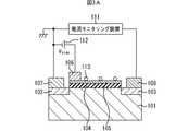
- FIG. 3A is a diagram illustrating a method of using the gas sensor according to the first embodiment.
- the gas sensor 100 is used by connecting, for example, a current monitoring device 111 that detects a current flowing between a source electrode 107 and a drain electrode 108 between them.
- the source electrode 107 is grounded, and a bias voltage V bias is applied to the gate electrode 106 by a bias power source 112.
- the current monitoring device 111 may include, for example, various power supplies, amplifier circuits, sampling circuits, analog-digital (AD) converters, data processing computers, and the like.
- FIG. 3B shows a band diagram of the graphene film 105, the insulating film 104, and the p-type layer 101.
- V FB ⁇ g - ⁇ s
- the drain current at the same bias point V bias is changed from I d1 to I d2 by [Delta] I d.
- the current monitoring device 111 may graphene film 105 to identify the number of ammonia molecules 113 adsorbed, it is possible to identify the concentration of ammonia from this number.
- Variation [Delta] I d is an example of a physical quantity.
- the drain current changes exponentially. Therefore, even a small amount of change in the work function of the graphene layer 105 may be a variation [Delta] I d of the drain current large.
- the work function change amount is 60 mV
- 1000% can be obtained as a single-digit change amount, that is, ⁇ I d / I d1 .
- the absolute change of the drain current can be set near the maximum current of the field effect transistor. According to the present embodiment, ppb level ammonia can be easily detected.
- the number of graphene unit layers included in the graphene film 105 is not limited, but it is preferably 1 to 100 layers in consideration of the ease of the manufacturing process and the (parasitic) resistance of the graphene film 105 itself. It is particularly preferred. In order to obtain higher sensitivity, it is preferable that the area of the portion of the graphene film 105 in contact with the gas is larger than the area of the portion covered with the protective film or the electrode.
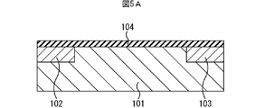
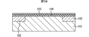
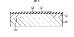
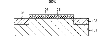
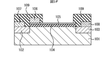
- 5A to 5F are cross-sectional views showing the method of manufacturing the gas sensor according to the first embodiment in the order of steps.
- an n-type layer 102 and an n-type layer 103 are formed on the surface of the p-type layer 101.
- the p-type layer 101 can be formed by ion implantation of p-type impurities into the surface of a silicon substrate, and the n-type layer 102 and the n-type layer 103 are ion-implanted with n-type impurities into the surface of the p-type layer 101. Can be formed.
- an insulating film 104 is formed over the p-type layer 101, the n-type layer 102, and the n-type layer 103.
- the insulating film 104 can be formed by thermal oxidation of the surfaces of the p-type layer 101, the n-type layer 102, and the n-type layer 103, for example.
- a graphene film 105 is provided on the insulating film 104.
- the graphene film 105 can be formed, for example, by growth and transfer onto a growth substrate described later.
- the graphene film 105 is patterned.
- the graphene film 105 can be patterned by, for example, a photolithography technique and an etching technique.
- the etching technique include reactive ion etching (RIE) using oxygen plasma.
- the insulating film 104 is patterned to expose at least part of the n-type layer 102 and at least part of the n-type layer 103.
- the insulating film 104 can be patterned by, for example, a photolithography technique and an etching technique.
- a gate electrode 106 is formed on the graphene film 105, a source electrode 107 is formed on the n-type layer 102, and a drain electrode 108 is formed on the n-type layer 103.
- a mask that exposes a region where these are to be formed is formed, a metal film is formed by vacuum deposition, and the mask is formed together with the metal film thereon. Remove. That is, the gate electrode 106, the source electrode 107, and the drain electrode 108 can be formed by a lift-off method.
- the metal film for example, a Ti film having a thickness of 5 nm is formed, and an Au film having a thickness of 200 nm is formed thereon.
- a protective film 109 that covers the gate electrode 106, the source electrode 107, and the drain electrode 108 and exposes at least a part of the graphene film 105 is formed.
- the gas sensor according to the first embodiment can be manufactured.
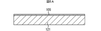
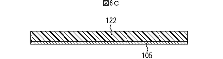
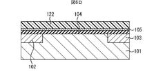
- 6A to 6D are cross-sectional views illustrating a method of providing the graphene film 105 over the insulating film 104 in the order of steps.
- a graphene film 105 is grown on a growth substrate 121 having a catalytic action.
- a growth substrate 121 for example, a Cu substrate can be used.
- the graphene film 105 can be grown using, for example, a chemical vapor deposition (CVD) synthesis furnace.
- the temperature of the growth substrate 121 is 1000 ° C.
- a mixed gas of H 2 and CH 4 is used as the source gas
- the flow rate of H 2 is 500 times the flow rate of CH 4
- the total pressure is 760 Torr.
- a support 122 is formed on the graphene film 105.
- a polymethyl methacrylate (PMMA) film can be used as the support 122.
- the growth substrate 121 is removed.
- the growth substrate 121 can be dissolved in, for example, an iron chloride solution.
- the graphene film 105 is disposed on the insulating film 104. Then, the support 122 is removed using an organic solvent.
- the graphene film 105 can be provided on the insulating film 104 by transfer.
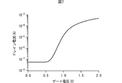
- the inventors manufactured the gas sensor according to the first embodiment, and measured the dependency of the drain current on the gate voltage. The result is shown in FIG.
- the channel length of this gas sensor was about 5 ⁇ m
- the thickness of the gate oxide film was about 14 nm
- the drain voltage was 1V.
- the transistor included in this gas sensor is an enhanced type.
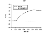
- the horizontal axis represents elapsed time
- the vertical axis represents the ratio of the drain current Id to the drain current Id 0 at the start of measurement (Id / Id 0 ).
- the gate voltage was 800 mV and the drain voltage was 1V.
- the rate of change of the drain current in the reference example is about 1%, whereas the rate of change of several tens of percent was obtained in the gas sensor according to the first embodiment. This means that the gas sensor according to the first embodiment has a significantly higher sensitivity to ammonia than the reference example.
- FIG. 10 is a cross-sectional view showing the structure of the gas sensor according to the second embodiment.
- the gas sensor 200 includes a p-type layer 101, an n-type layer 102, an n-type layer 103, an insulating film 104, and a source electrode 107, as in the first embodiment. And a drain electrode 108 are included.
- the gas sensor 200 further includes a gate electrode 206 on the insulating film 104, an interlayer insulating film 221 covering the insulating film 104, and a conductive layer 222 provided in the interlayer insulating film 221 and in contact with the gate electrode 206.
- the gas sensor 200 includes a graphene film 205 that covers the upper surfaces of the interlayer insulating film 221 and the conductive layer 222 and is in contact with the conductive layer 222.
- the graphene film 205 is in electrical contact with the insulating film 104 through the conductive layer 222 in the interlayer insulating film 221.
- Examples of the material of the gate electrode 206 include polycrystalline Si and metal.
- the conductive layer 222 is a conductive via such as a metal via.
- the work function of the graphene film 205 is greatly changed even if the amount is small. Since the graphene film 205 is in contact with the conductive layer 222 and the conductive layer 222 is in contact with the gate electrode 206, the change in work function of the graphene film 205 is transmitted to the gate electrode 206. Therefore, it is possible in the same manner as in the first embodiment, to measure the amount of change [Delta] I d of the corresponding drain currents of change work function of graphene film 205.
- the area of the graphene film 205 in contact with the gas in the second embodiment is larger than the area of the graphene film 105 in contact with the gas in the first embodiment. Therefore, according to the second embodiment, the ammonia concentration can be measured with higher sensitivity.
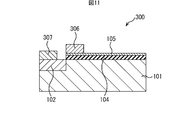
- FIG. 11 is a cross-sectional view showing the structure of the gas sensor according to the third embodiment.
- the gas sensor 300 includes a p-type layer 101, an n-type layer 102, an insulating film 104, and a graphene film 105 as in the first embodiment.
- the gas sensor 300 further includes an electrode 306 similar to the gate electrode 106 and an electrode 307 similar to the source electrode 107.
- the amount of change in the work function of the graphene film 105 accompanying the adsorption of ammonia molecules appears as the amount of change ⁇ C in the capacitance between the electrode 306 and the electrode 307. . Therefore, the ammonia concentration can be specified by measuring the amount of change ⁇ C. According to such 3rd Embodiment, size reduction and cost reduction accompanying this are possible with respect to 1st Embodiment. In addition, power can be saved because measurement can be performed without flowing a drain current.
- the change amount ⁇ C is an example of a physical quantity.
- FIG. 12A is a cross-sectional view showing the structure of the gas sensor according to the fourth embodiment.
- the gas sensor 400 according to the fourth embodiment includes nanoparticles 411 that change the work function of graphene on the graphene film 105 as shown in FIG. 12A.
- Other configurations are the same as those of the first embodiment.
- the particle diameter of the nanoparticles 411 is about 1 nm to 100 nm, and the coverage of the graphene film 105 by the nanoparticles 411 is about 5% to 100%, but is not limited thereto.
- Examples of the material of the nanoparticles 411 include gold, silver, copper, scandium, titanium, vanadium, chromium, manganese, iron, cobalt, nickel, zinc, aluminum, yttrium, zirconium, niobium, molybdenum, ruthenium, rhodium, palladium, Examples include metals such as hafnium, tantalum, tungsten, osnium, iridium and platinum. An oxide of these metals may be used as the material of the nanoparticles 411. As a material of the nanoparticles 411, a semiconductor such as silicon, germanium, zinc oxide, or tin oxide may be used. A plurality of types of nanoparticles 411 having different materials may be mixed on the graphene film 105.
- the sensitivity is different from that of the first embodiment, and high sensitivity can be exhibited for gases other than ammonia and nitrogen dioxide.
- the nanoparticle 411 itself reacts with the gas to change the state of the nanoparticle 411, which may change the sensitivity.
- palladium nanoparticles absorb hydrogen, and the work function at the interface of palladium with graphene changes, and as a result, the work function of graphene also changes. For this reason, the threshold voltage of the transistor changes and the drain current of the channel changes.
- the nanoparticles of nickel, cobalt, or iron adsorb hydrocarbon-based gases such as methane and acetylene, when the nanoparticles 411 include nickel, cobalt, or iron, the gas sensor 400 serves as a hydrocarbon-based gas sensor. Can function.
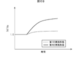
- FIG. 12B shows a response example of the gas sensor 400 using the Pd nanoparticles 411.
- the transistor included in the gas sensor 400 is an n-channel transistor.
- the threshold voltage changes to the negative side, and if the gate voltage is the same, the drain current increases.
- the sensitivity to hydrogen is higher than that of the first embodiment.
- FIG. 13 is a diagram illustrating an example of an apparatus used for deposition of the nanoparticles 411.
- nanoparticles are generated by laser ablation in low-pressure He gas. Specifically, 1 slpm (standard liter per minute) to 2 slpm of He gas is introduced into the generation chamber 61, and the pressure in the generation chamber 61 is adjusted to about 1 kPa. Then, a metal target 62 installed in the generation chamber 61, for example, a Co target is irradiated with a pulse laser 63.
- the pulse laser 63 for example, a YAG (YttriumnetAluminum Garnet) laser double wave (532 nm) is used, the power is 2 W, and the pulse repetition frequency is 20 Hz.
- a metal vapor is generated from the metal target 62 by laser irradiation and the metal vapor is quenched with He gas, particles having a particle size of about 1 nm to 100 nm are formed. Particles having a particle size of about 1 nm to 100 nm are called nanoparticles.
- the particles are sent to a fine particle size selection unit (impactor) 64 by He gas.
- the impactor 64 is a device that removes particles of a certain size or more due to the inertia of the particles. Since nanoparticles generally grow with time due to aggregation or the like, there is a lower limit to the size of the nanoparticles. Therefore, if nanoparticles larger than a certain size are removed by the impactor 64, the size of the nanoparticles passing through the impactor 64 is controlled.
- the impactor 64 is used under the condition that the diameter of the nanoparticles passing through the impactor 64 is about 5 nm.
- the nanoparticles whose size is selected by the impactor 64 are then guided to the deposition chamber 70 having a pressure of about 10 ⁇ 3 Pa to which the pump 67 is connected by differential evacuation using the pumps 65 and 66.
- the nanoparticles become a beam and are deposited by colliding with the substrate 69 placed on the stage 68 almost vertically.
- the nanoparticles 411 are randomly arranged without being closely packed. According to this method, it is possible to deposit nanoparticles 411 that are extremely uniform in size, highly crystalline, and have a clean surface.
- lithography may be used to open only the channel part and deposit nanoparticles only in the channel part.
- Non-patent Document A-2 Sato et al., Sensors and Materials, 21, 373 (2009)” and the document “Sato et al., Chem. Phys. Lett. 382, 361 ( 2003) ”.
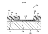
- FIG. 14A is a cross-sectional view showing the structure of the gas sensor according to the fifth embodiment.
- the gas sensor 500 according to the fifth embodiment includes a graphene nanomesh 512 instead of the graphene film 105, as shown in FIG. 14A.
- the graphene nanomesh 512 is configured, for example, by forming a plurality of holes 514 in the graphene film 105.
- the size and space of the hole 514 is, for example, about 1 nm to 50 nm.
- the formation of the holes 514 changes the electronic state of the graphene film 105, and the manner of gas molecule adsorption to the graphene film 105 and the change in work function accompanying the adsorption are different. For this reason, the sensitivity is different from that of the first embodiment, and high sensitivity can be exhibited for gases other than ammonia and nitrogen dioxide.
- the edge of the hole 514 may be chemically modified with a specific atom or molecule such as H, F, NH 2 , CH 3 , Cl, Br, OH, COOH.
- a specific atom or molecule such as H, F, NH 2 , CH 3 , Cl, Br, OH, COOH.
- the reactivity or sensitivity of the gas sensor 500 can be adjusted by chemical modification.
- nanoparticles 411 may enter part or all of the holes 514. Also in this case, the reactivity or sensitivity of the gas sensor 500 can be adjusted.
- This structure can be obtained, for example, by depositing the nanoparticles 411 by laser ablation as in the fourth embodiment and then allowing the nanoparticles 411 to absorb the carbon of the graphene film 105 by heating.
- the graphene nanomesh 512 is obtained by removing the nanoparticles 411 that have absorbed carbon in the graphene film 105 using an acidic solution such as dilute hydrochloric acid or an aqueous iron chloride solution.
- Examples of semiconductor layer materials include group IV semiconductors, group III-V compound semiconductors, group II-VI compound semiconductors, oxide semiconductors, organic semiconductors, metal chalcogenide semiconductors, layered material semiconductors, semiconductor carbon nanotubes, and graphene nanoribbons.
- Examples of the group IV semiconductor include single crystal Si and polycrystalline Si.
- Examples of III-V compound semiconductors include arsenide semiconductors such as GaAs and nitride semiconductors such as GaN.
- CdTe is exemplified as the II-VI group compound semiconductor.
- ZnO is exemplified as the oxide semiconductor.
- An example of the organic semiconductor is pentacene.
- MoS 2 is exemplified as the metal chalcogenide-based semiconductor.
- black phosphorus is exemplified.
- Examples of the material of the insulating film 104 include silicon oxide, silicon nitride, silicon oxynitride, germanium oxide, a high dielectric constant insulator, and a layered insulator.
- Examples of the high dielectric constant insulator include an insulator including aluminum, titanium, tantalum, hafnium, or any combination thereof, for example, aluminum oxide and hafnium oxide.
- Examples of the layered insulator include hexagonal boron nitride (BN) and hexagonal boron carbonitride (BCN) which is a mixed crystal of boron nitride and graphite.
- the barrier film is not limited to an insulating film.
- a III-V compound semiconductor or a II-VI group compound semiconductor having a wider band gap than the compound semiconductor of the semiconductor layer can be used as the barrier film.
- a combination of materials of the semiconductor layer and the barrier film a combination of GaAs and AlGaAs, a combination of InGaAs and InAlAs, and a combination of GaN and AlGaN are exemplified.
- the protective film 109 may be omitted depending on the application and environment.
- the type of gas to be detected is not limited to ammonia.
- the conductivity types of the semiconductor layers in these embodiments may be reversed. That is, an n-type layer may be used instead of the p-type layer 101, a p-type layer may be used instead of the n-type layer 102, and a p-type layer may be used instead of the n-type layer 103.
- a gas such as ammonia can be detected with high sensitivity.
Landscapes
- Chemical & Material Sciences (AREA)
- Health & Medical Sciences (AREA)
- Engineering & Computer Science (AREA)
- Life Sciences & Earth Sciences (AREA)
- General Health & Medical Sciences (AREA)
- Pathology (AREA)
- Physics & Mathematics (AREA)
- Immunology (AREA)
- Analytical Chemistry (AREA)
- Biochemistry (AREA)
- General Physics & Mathematics (AREA)
- Nanotechnology (AREA)
- Chemical Kinetics & Catalysis (AREA)
- Electrochemistry (AREA)
- Combustion & Propulsion (AREA)
- Food Science & Technology (AREA)
- Medicinal Chemistry (AREA)
- Microelectronics & Electronic Packaging (AREA)
- Molecular Biology (AREA)
- Investigating Or Analyzing Materials By The Use Of Electric Means (AREA)
- Investigating Or Analyzing Materials By The Use Of Fluid Adsorption Or Reactions (AREA)
Abstract
La présente invention comprend : des couches à semi-conducteur (101-103) ; un film de graphène (105) qui est prévu au-dessus des couches à semi-conducteur (101-103), au moins une section de celui-ci venant en contact avec un gaz ; et un film barrière (104) entre les couches à semi-conducteur (101-103) et le film de graphène (105).
Priority Applications (3)
| Application Number | Priority Date | Filing Date | Title |
|---|---|---|---|
| JP2017526396A JP6687862B2 (ja) | 2015-06-30 | 2016-06-29 | ガスセンサ及びその使用方法 |
| CN201680038272.8A CN107709979B (zh) | 2015-06-30 | 2016-06-29 | 气体传感器及其使用方法 |
| US15/854,901 US11156576B2 (en) | 2015-06-30 | 2017-12-27 | Gas sensor and method of using the same |
Applications Claiming Priority (2)
| Application Number | Priority Date | Filing Date | Title |
|---|---|---|---|
| JP2015131229 | 2015-06-30 | ||
| JP2015-131229 | 2015-06-30 |
Related Child Applications (1)
| Application Number | Title | Priority Date | Filing Date |
|---|---|---|---|
| US15/854,901 Continuation US11156576B2 (en) | 2015-06-30 | 2017-12-27 | Gas sensor and method of using the same |
Publications (1)
| Publication Number | Publication Date |
|---|---|
| WO2017002854A1 true WO2017002854A1 (fr) | 2017-01-05 |
Family
ID=57609307
Family Applications (1)
| Application Number | Title | Priority Date | Filing Date |
|---|---|---|---|
| PCT/JP2016/069267 Ceased WO2017002854A1 (fr) | 2015-06-30 | 2016-06-29 | Capteur de gaz et son procédé de fabrication |
Country Status (4)
| Country | Link |
|---|---|
| US (1) | US11156576B2 (fr) |
| JP (1) | JP6687862B2 (fr) |
| CN (1) | CN107709979B (fr) |
| WO (1) | WO2017002854A1 (fr) |
Cited By (10)
| Publication number | Priority date | Publication date | Assignee | Title |
|---|---|---|---|---|
| CN108892125A (zh) * | 2018-07-10 | 2018-11-27 | 浙江大学 | 一种气体分子探测膜 |
| JP2019020153A (ja) * | 2017-07-12 | 2019-02-07 | 富士通株式会社 | トランジスタ及びその製造方法 |
| JP2019102567A (ja) * | 2017-11-30 | 2019-06-24 | 富士通株式会社 | 電子デバイス、電子デバイスの製造方法及び電子機器 |
| TWI695168B (zh) * | 2019-05-22 | 2020-06-01 | 長庚大學 | 氣體感測裝置及其製作方法 |
| JP2020204486A (ja) * | 2019-06-14 | 2020-12-24 | 富士通株式会社 | ガスセンサ、及びガスセンサの製造方法 |
| JPWO2021040050A1 (fr) * | 2019-08-30 | 2021-03-04 | ||
| US11029271B2 (en) * | 2018-10-19 | 2021-06-08 | Korea Institute Of Science And Technology | Ammonia gas detecting sensor using graphene doped with copper oxide nanopaticles and ammonia gas detecting device comprising the same |
| JP2023526622A (ja) * | 2020-05-26 | 2023-06-22 | リージェンツ・オブ・ザ・ユニバーシティ・オブ・ミネソタ | ナノ粒子を有するグラフェンの非共有結合修飾 |
| JP2023111672A (ja) * | 2022-01-31 | 2023-08-10 | 太陽誘電株式会社 | ガスセンサ |
| US12604506B2 (en) | 2019-08-20 | 2026-04-14 | Regents Of The University Of Minnesota | Non-covalent modification of graphene-based chemical sensors |
Families Citing this family (18)
| Publication number | Priority date | Publication date | Assignee | Title |
|---|---|---|---|---|
| TWI610078B (zh) * | 2016-11-15 | 2018-01-01 | National Sun Yat-Sen University | 氣體檢測模組及其氣體感測器 |
| US12119462B2 (en) | 2018-01-04 | 2024-10-15 | Lyten, Inc. | Sensing device for detecting analytes in batteries |
| CN112105922B (zh) * | 2018-01-04 | 2024-09-03 | 利腾股份有限公司 | 谐振气体传感器 |
| US11137368B2 (en) | 2018-01-04 | 2021-10-05 | Lyten, Inc. | Resonant gas sensor |
| US11988628B2 (en) | 2018-01-04 | 2024-05-21 | Lyten, Inc. | Container including analyte sensing device |
| US11913901B2 (en) | 2018-01-04 | 2024-02-27 | Lyten, Inc. | Analyte sensing device |
| JP6806724B2 (ja) * | 2018-03-22 | 2021-01-06 | 株式会社東芝 | 分子検出素子及び分子検出装置 |
| CN109448798B (zh) * | 2018-11-30 | 2021-09-03 | 湘潭大学 | 一种分子动力学模拟二元掺杂离子液体润滑薄膜结构特性的方法 |
| CN110514698B (zh) * | 2019-09-27 | 2022-09-30 | 福州京东方光电科技有限公司 | 一种气体感测装置和气体检测设备 |
| EP3819260A1 (fr) * | 2019-11-07 | 2021-05-12 | Infineon Technologies AG | Matériau composite, capteur de gaz chimiorésistant, système de capteur de gaz chimiorésistant et son procédé de fabrication et d'utilisation |
| US12480910B2 (en) | 2019-12-30 | 2025-11-25 | The Regents Of The University Of California | Multi-gas detection with CS-FET arrays for food quality assessment |
| US12352723B2 (en) | 2020-06-23 | 2025-07-08 | Lyten, Inc. | Biofunctionalized three-dimensional (3D) graphene-based field-effect transistor (FET) sensor |
| US11988629B2 (en) | 2020-06-23 | 2024-05-21 | Lyten, Inc. | Method of manufacturing a graphene-based biological field-effect transistor |
| EP4001906B1 (fr) * | 2020-11-20 | 2024-10-02 | Infineon Technologies AG | Dispositif sensible au gaz |
| CN112505108B (zh) * | 2020-12-18 | 2021-07-06 | 联合微电子中心有限责任公司 | 气体检测系统和方法 |
| US12369815B2 (en) | 2021-03-16 | 2025-07-29 | Regents Of The University Of Minnesota | Aldehyde and ketone receptor modification of graphene |
| CN116593538A (zh) * | 2023-04-28 | 2023-08-15 | 太原理工大学 | 一种GaN/rGO氨气传感器及其制备方法 |
| CN119757496B (zh) * | 2024-11-06 | 2026-02-24 | 山东大学 | 一种基于有机垂直源栅晶体管二氧化氮传感器及其制备方法 |
Citations (8)
| Publication number | Priority date | Publication date | Assignee | Title |
|---|---|---|---|---|
| JPS6133645A (ja) * | 1984-07-25 | 1986-02-17 | 住友電気工業株式会社 | 生体用センサ− |
| US20100025660A1 (en) * | 2008-07-31 | 2010-02-04 | University Of Connecticut | Semiconductor devices, methods of manufacture thereof and articles comprising the same |
| US20120171775A1 (en) * | 2007-08-07 | 2012-07-05 | University Of South Carolina | Multi-dimensional integrated detection and analysis system (midas) based on microcantilvers |
| JP2012202864A (ja) * | 2011-03-25 | 2012-10-22 | Rohm Co Ltd | Isfetおよびisfetアレイ |
| WO2012150884A1 (fr) * | 2011-05-05 | 2012-11-08 | Sensic Ab | Transistor à effet de champ pour la détection chimique au moyen de graphène, capteur chimique doté de ce transistor et procédé de production du transistor |
| JP2012247189A (ja) * | 2011-05-25 | 2012-12-13 | Hitachi Ltd | グラフェンセンサ、該センサを利用した物質種分析装置および該センサを利用した物質種検知方法 |
| US20140151631A1 (en) * | 2012-11-20 | 2014-06-05 | The Provost, Fellows, Foundation Scholars, And The Other Members Of Board, Of | Asymmetric bottom contacted device |
| WO2015007947A1 (fr) * | 2013-07-16 | 2015-01-22 | Nokia Corporation | Capteur environnemental et procédé pour déterminer la tension de vapeur relative |
Family Cites Families (13)
| Publication number | Priority date | Publication date | Assignee | Title |
|---|---|---|---|---|
| JPS60181645A (ja) * | 1984-02-28 | 1985-09-17 | Sharp Corp | 複合センサ及びその製造方法 |
| JPH09159633A (ja) | 1995-12-05 | 1997-06-20 | Tokyo Gas Co Ltd | ガスセンサ |
| JP3555739B2 (ja) | 1998-08-18 | 2004-08-18 | 富士電機機器制御株式会社 | 薄膜ガスセンサの製造方法 |
| JP4866880B2 (ja) | 2008-06-16 | 2012-02-01 | 株式会社日立製作所 | 電極、ガスセンサおよびその製造方法 |
| KR20100035380A (ko) | 2008-09-26 | 2010-04-05 | 삼성전자주식회사 | 박막형 센싱부재를 이용한 화학 센서 |
| US20110138882A1 (en) * | 2009-12-11 | 2011-06-16 | Electronics And Telecommunications Research Institute | Semiconductor gas sensor having low power consumption |
| JP2011169634A (ja) | 2010-02-16 | 2011-09-01 | Fuji Electric Co Ltd | 薄膜ガスセンサ |
| JP5603193B2 (ja) | 2010-09-29 | 2014-10-08 | 株式会社日立製作所 | ガスセンサ |
| CN102778481B (zh) * | 2011-05-09 | 2014-06-11 | 中国科学院微电子研究所 | 感应栅型非晶态金属氧化物tft气体传感器 |
| DE102011118930A1 (de) | 2011-11-21 | 2013-05-23 | Micronas Gmbh | Halbleiter-Gassensor |
| US8901680B2 (en) * | 2012-04-12 | 2014-12-02 | International Business Machines Corporation | Graphene pressure sensors |
| JP6533465B2 (ja) * | 2012-10-16 | 2019-06-19 | コーニンクレッカ フィリップス エヌ ヴェKoninklijke Philips N.V. | ナノワイヤプラットフォームに基づく広いダイナミックレンジを持つ流体センサ |
| US20140260545A1 (en) * | 2013-03-15 | 2014-09-18 | Infineon Technologies Ag | Sensor and sensing method |
-
2016
- 2016-06-29 WO PCT/JP2016/069267 patent/WO2017002854A1/fr not_active Ceased
- 2016-06-29 CN CN201680038272.8A patent/CN107709979B/zh not_active Expired - Fee Related
- 2016-06-29 JP JP2017526396A patent/JP6687862B2/ja not_active Expired - Fee Related
-
2017
- 2017-12-27 US US15/854,901 patent/US11156576B2/en not_active Expired - Fee Related
Patent Citations (8)
| Publication number | Priority date | Publication date | Assignee | Title |
|---|---|---|---|---|
| JPS6133645A (ja) * | 1984-07-25 | 1986-02-17 | 住友電気工業株式会社 | 生体用センサ− |
| US20120171775A1 (en) * | 2007-08-07 | 2012-07-05 | University Of South Carolina | Multi-dimensional integrated detection and analysis system (midas) based on microcantilvers |
| US20100025660A1 (en) * | 2008-07-31 | 2010-02-04 | University Of Connecticut | Semiconductor devices, methods of manufacture thereof and articles comprising the same |
| JP2012202864A (ja) * | 2011-03-25 | 2012-10-22 | Rohm Co Ltd | Isfetおよびisfetアレイ |
| WO2012150884A1 (fr) * | 2011-05-05 | 2012-11-08 | Sensic Ab | Transistor à effet de champ pour la détection chimique au moyen de graphène, capteur chimique doté de ce transistor et procédé de production du transistor |
| JP2012247189A (ja) * | 2011-05-25 | 2012-12-13 | Hitachi Ltd | グラフェンセンサ、該センサを利用した物質種分析装置および該センサを利用した物質種検知方法 |
| US20140151631A1 (en) * | 2012-11-20 | 2014-06-05 | The Provost, Fellows, Foundation Scholars, And The Other Members Of Board, Of | Asymmetric bottom contacted device |
| WO2015007947A1 (fr) * | 2013-07-16 | 2015-01-22 | Nokia Corporation | Capteur environnemental et procédé pour déterminer la tension de vapeur relative |
Cited By (16)
| Publication number | Priority date | Publication date | Assignee | Title |
|---|---|---|---|---|
| JP2019020153A (ja) * | 2017-07-12 | 2019-02-07 | 富士通株式会社 | トランジスタ及びその製造方法 |
| JP2019102567A (ja) * | 2017-11-30 | 2019-06-24 | 富士通株式会社 | 電子デバイス、電子デバイスの製造方法及び電子機器 |
| US10734495B2 (en) | 2017-11-30 | 2020-08-04 | Fujitsu Limited | Electronic device, manufacturing method for electronic device, and electronic apparatus |
| CN108892125B (zh) * | 2018-07-10 | 2020-06-30 | 浙江大学 | 一种气体分子探测膜 |
| CN108892125A (zh) * | 2018-07-10 | 2018-11-27 | 浙江大学 | 一种气体分子探测膜 |
| US11029271B2 (en) * | 2018-10-19 | 2021-06-08 | Korea Institute Of Science And Technology | Ammonia gas detecting sensor using graphene doped with copper oxide nanopaticles and ammonia gas detecting device comprising the same |
| TWI695168B (zh) * | 2019-05-22 | 2020-06-01 | 長庚大學 | 氣體感測裝置及其製作方法 |
| JP7215347B2 (ja) | 2019-06-14 | 2023-01-31 | 富士通株式会社 | ガスセンサ、及びガスセンサの製造方法 |
| JP2020204486A (ja) * | 2019-06-14 | 2020-12-24 | 富士通株式会社 | ガスセンサ、及びガスセンサの製造方法 |
| US12604506B2 (en) | 2019-08-20 | 2026-04-14 | Regents Of The University Of Minnesota | Non-covalent modification of graphene-based chemical sensors |
| WO2021040050A1 (fr) * | 2019-08-30 | 2021-03-04 | 太陽誘電株式会社 | Dispositif de détermination de gaz, procédé de détermination de gaz et système de détermination de gaz |
| JP7189364B2 (ja) | 2019-08-30 | 2022-12-13 | 太陽誘電株式会社 | ガス判定装置、ガス判定方法及びガス判定システム |
| JPWO2021040050A1 (fr) * | 2019-08-30 | 2021-03-04 | ||
| JP2023526622A (ja) * | 2020-05-26 | 2023-06-22 | リージェンツ・オブ・ザ・ユニバーシティ・オブ・ミネソタ | ナノ粒子を有するグラフェンの非共有結合修飾 |
| JP2023111672A (ja) * | 2022-01-31 | 2023-08-10 | 太陽誘電株式会社 | ガスセンサ |
| JP7822805B2 (ja) | 2022-01-31 | 2026-03-03 | 太陽誘電株式会社 | ガスセンサ |
Also Published As
| Publication number | Publication date |
|---|---|
| JPWO2017002854A1 (ja) | 2018-04-19 |
| JP6687862B2 (ja) | 2020-04-28 |
| CN107709979A (zh) | 2018-02-16 |
| CN107709979B (zh) | 2020-07-07 |
| US11156576B2 (en) | 2021-10-26 |
| US20180136157A1 (en) | 2018-05-17 |
Similar Documents
| Publication | Publication Date | Title |
|---|---|---|
| JP6687862B2 (ja) | ガスセンサ及びその使用方法 | |
| Pham et al. | MoS2-graphene heterostructures as efficient organic compounds sensing 2D materials | |
| Baek et al. | A highly sensitive chemical gas detecting transistor based on highly crystalline CVD-grown MoSe2 films | |
| Bag et al. | Gas sensing with heterostructures based on two-dimensional nanostructured materials: a review | |
| Ma et al. | Black phosphorus field-effect transistors with work function tunable contacts | |
| Wu et al. | Wafer-scale synthesis of graphene by chemical vapor deposition and its application in hydrogen sensing | |
| Kim et al. | Chemically modulated graphene diodes | |
| Voiry et al. | The role of electronic coupling between substrate and 2D MoS2 nanosheets in electrocatalytic production of hydrogen | |
| Mashock et al. | Modulating gas sensing properties of CuO nanowires through creation of discrete nanosized p–n junctions on their surfaces | |
| Yamamoto et al. | Anisotropic etching of atomically thin MoS2 | |
| Late et al. | Sensing behavior of atomically thin-layered MoS2 transistors | |
| Wang et al. | Negligible environmental sensitivity of graphene in a hexagonal boron nitride/graphene/h-BN sandwich structure | |
| US10648959B2 (en) | Black phosphorus gas sensor | |
| Kumar et al. | Enhanced thermionic emission and low 1/f noise in exfoliated graphene/GaN Schottky barrier diode | |
| Smyth et al. | Engineering the palladium–WSe2 interface chemistry for field effect transistors with high-performance hole contacts | |
| Kang et al. | High-performance electrically transduced hazardous gas sensors based on low-dimensional nanomaterials | |
| JP6413824B2 (ja) | ガスセンサ及びその製造方法 | |
| Das et al. | Facile synthesis of 2D-HfS 2 flakes for $\mu $-IDE-based methanol sensor: fast detection at room temperature | |
| Loes et al. | Synergistic Effect of TiS3 and Ti3C2T x MXene for Temperature-Tunable p-/n-Type Gas Sensing | |
| Amin et al. | Graphene as a sensor | |
| Chee et al. | Defect-assisted contact property enhancement in a molybdenum disulfide monolayer | |
| Su et al. | Promising approach for high-performance MoS2 nanodevice: doping the BN buffer layer to eliminate the Schottky barriers | |
| Zheng et al. | Reversible n-type doping of graphene by H2O-based atomic-layer deposition and its doping mechanism | |
| Liu et al. | A carbon-based FET-type sensor with floating sensing gate for ppb-level ammonia detection at room temperature | |
| Noll et al. | Transfer-free in situ ccvd grown nanocrystalline graphene for sub-ppmv ammonia detection |
Legal Events
| Date | Code | Title | Description |
|---|---|---|---|
| 121 | Ep: the epo has been informed by wipo that ep was designated in this application |
Ref document number: 16817962 Country of ref document: EP Kind code of ref document: A1 |
|
| ENP | Entry into the national phase |
Ref document number: 2017526396 Country of ref document: JP Kind code of ref document: A |
|
| NENP | Non-entry into the national phase |
Ref country code: DE |
|
| 122 | Ep: pct application non-entry in european phase |
Ref document number: 16817962 Country of ref document: EP Kind code of ref document: A1 |