WO2017006520A1 - Dispositif d'imagerie - Google Patents
Dispositif d'imagerie Download PDFInfo
- Publication number
- WO2017006520A1 WO2017006520A1 PCT/JP2016/002917 JP2016002917W WO2017006520A1 WO 2017006520 A1 WO2017006520 A1 WO 2017006520A1 JP 2016002917 W JP2016002917 W JP 2016002917W WO 2017006520 A1 WO2017006520 A1 WO 2017006520A1
- Authority
- WO
- WIPO (PCT)
- Prior art keywords
- semiconductor
- carbon nanotube
- charge
- photoelectric conversion
- conversion layer
- Prior art date
- Legal status (The legal status is an assumption and is not a legal conclusion. Google has not performed a legal analysis and makes no representation as to the accuracy of the status listed.)
- Ceased
Links
Images




Classifications
-
- H—ELECTRICITY
- H10—SEMICONDUCTOR DEVICES; ELECTRIC SOLID-STATE DEVICES NOT OTHERWISE PROVIDED FOR
- H10K—ORGANIC ELECTRIC SOLID-STATE DEVICES
- H10K85/00—Organic materials used in the body or electrodes of devices covered by this subclass
- H10K85/20—Carbon compounds, e.g. carbon nanotubes or fullerenes
- H10K85/221—Carbon nanotubes
-
- H—ELECTRICITY
- H04—ELECTRIC COMMUNICATION TECHNIQUE
- H04N—PICTORIAL COMMUNICATION, e.g. TELEVISION
- H04N25/00—Circuitry of solid-state image sensors [SSIS]; Control thereof
- H04N25/70—SSIS architectures; Circuits associated therewith
- H04N25/76—Addressed sensors, e.g. MOS or CMOS sensors
-
- H—ELECTRICITY
- H10—SEMICONDUCTOR DEVICES; ELECTRIC SOLID-STATE DEVICES NOT OTHERWISE PROVIDED FOR
- H10F—INORGANIC SEMICONDUCTOR DEVICES SENSITIVE TO INFRARED RADIATION, LIGHT, ELECTROMAGNETIC RADIATION OF SHORTER WAVELENGTH OR CORPUSCULAR RADIATION
- H10F30/00—Individual radiation-sensitive semiconductor devices in which radiation controls the flow of current through the devices, e.g. photodetectors
- H10F30/20—Individual radiation-sensitive semiconductor devices in which radiation controls the flow of current through the devices, e.g. photodetectors the devices having potential barriers, e.g. phototransistors
-
- H—ELECTRICITY
- H10—SEMICONDUCTOR DEVICES; ELECTRIC SOLID-STATE DEVICES NOT OTHERWISE PROVIDED FOR
- H10F—INORGANIC SEMICONDUCTOR DEVICES SENSITIVE TO INFRARED RADIATION, LIGHT, ELECTROMAGNETIC RADIATION OF SHORTER WAVELENGTH OR CORPUSCULAR RADIATION
- H10F39/00—Integrated devices, or assemblies of multiple devices, comprising at least one element covered by group H10F30/00, e.g. radiation detectors comprising photodiode arrays
- H10F39/10—Integrated devices
- H10F39/12—Image sensors
-
- H—ELECTRICITY
- H10—SEMICONDUCTOR DEVICES; ELECTRIC SOLID-STATE DEVICES NOT OTHERWISE PROVIDED FOR
- H10K—ORGANIC ELECTRIC SOLID-STATE DEVICES
- H10K30/00—Organic devices sensitive to infrared radiation, light, electromagnetic radiation of shorter wavelength or corpuscular radiation
- H10K30/30—Organic devices sensitive to infrared radiation, light, electromagnetic radiation of shorter wavelength or corpuscular radiation comprising bulk heterojunctions, e.g. interpenetrating networks of donor and acceptor material domains
- H10K30/353—Organic devices sensitive to infrared radiation, light, electromagnetic radiation of shorter wavelength or corpuscular radiation comprising bulk heterojunctions, e.g. interpenetrating networks of donor and acceptor material domains comprising blocking layers, e.g. exciton blocking layers
-
- H—ELECTRICITY
- H10—SEMICONDUCTOR DEVICES; ELECTRIC SOLID-STATE DEVICES NOT OTHERWISE PROVIDED FOR
- H10K—ORGANIC ELECTRIC SOLID-STATE DEVICES
- H10K39/00—Integrated devices, or assemblies of multiple devices, comprising at least one organic radiation-sensitive element covered by group H10K30/00
- H10K39/30—Devices controlled by radiation
- H10K39/32—Organic image sensors
-
- H—ELECTRICITY
- H10—SEMICONDUCTOR DEVICES; ELECTRIC SOLID-STATE DEVICES NOT OTHERWISE PROVIDED FOR
- H10K—ORGANIC ELECTRIC SOLID-STATE DEVICES
- H10K30/00—Organic devices sensitive to infrared radiation, light, electromagnetic radiation of shorter wavelength or corpuscular radiation
- H10K30/30—Organic devices sensitive to infrared radiation, light, electromagnetic radiation of shorter wavelength or corpuscular radiation comprising bulk heterojunctions, e.g. interpenetrating networks of donor and acceptor material domains
-
- H—ELECTRICITY
- H10—SEMICONDUCTOR DEVICES; ELECTRIC SOLID-STATE DEVICES NOT OTHERWISE PROVIDED FOR
- H10K—ORGANIC ELECTRIC SOLID-STATE DEVICES
- H10K85/00—Organic materials used in the body or electrodes of devices covered by this subclass
- H10K85/20—Carbon compounds, e.g. carbon nanotubes or fullerenes
- H10K85/211—Fullerenes, e.g. C60
-
- Y—GENERAL TAGGING OF NEW TECHNOLOGICAL DEVELOPMENTS; GENERAL TAGGING OF CROSS-SECTIONAL TECHNOLOGIES SPANNING OVER SEVERAL SECTIONS OF THE IPC; TECHNICAL SUBJECTS COVERED BY FORMER USPC CROSS-REFERENCE ART COLLECTIONS [XRACs] AND DIGESTS
- Y02—TECHNOLOGIES OR APPLICATIONS FOR MITIGATION OR ADAPTATION AGAINST CLIMATE CHANGE
- Y02E—REDUCTION OF GREENHOUSE GAS [GHG] EMISSIONS, RELATED TO ENERGY GENERATION, TRANSMISSION OR DISTRIBUTION
- Y02E10/00—Energy generation through renewable energy sources
- Y02E10/50—Photovoltaic [PV] energy
- Y02E10/549—Organic PV cells
Definitions
- This application relates to a multilayer imaging device.
- Patent Document 1 discloses an image sensor having high light utilization efficiency by including photoelectric conversion layers having sensitivity in two or more different wavelength bands.
- An imaging device is an imaging device including a plurality of pixels arranged in one or two dimensions, and each pixel is electrically connected between the plurality of pixels.
- a photoelectric conversion layer including a connected electrode, a charge collection unit partitioned for each pixel, and a photoelectric conversion layer located between the electrode and the charge collection unit and connected between the plurality of pixels, And a semiconductor-type carbon nanotube and one of a first substance having an electron affinity greater than that of the semiconductor-type carbon nanotube and a second substance having an ionization potential smaller than that of the semiconductor-type carbon nanotube.
- an imaging device including a carbon nanotube as a photoelectric conversion material is provided.
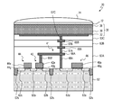
- FIG. 1 is a diagram illustrating an example of a circuit of the imaging device according to the first embodiment of the present disclosure.
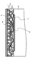
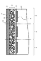
- FIG. 2 is a schematic cross-sectional view showing an example of a device structure in the unit pixel cell of the imaging apparatus shown in FIG. 3A is a schematic cross-sectional view illustrating an example of the structure of the photoelectric conversion unit of the imaging apparatus illustrated in FIG. 1.
- 3B is a schematic cross-sectional view illustrating another example of the structure of the photoelectric conversion unit of the imaging apparatus illustrated in FIG. 1.
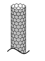
- FIG. 4A is a schematic diagram showing an example of the structure of a carbon nanotube.
- FIG. 4B is a schematic diagram for explaining the chirality of the carbon nanotube.
- FIG. 1 is a diagram illustrating an example of a circuit of the imaging device according to the first embodiment of the present disclosure.
- FIG. 2 is a schematic cross-sectional view showing an example of a device structure in the unit pixel cell of the imaging apparatus shown in FIG.
- 3A is a
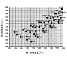
- FIG. 5 is a diagram showing the relationship between the chirality of carbon nanotubes and the first and second resonance wavelengths.
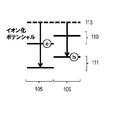
- FIG. 6A is a schematic diagram illustrating the magnitude relationship between the electron affinity of the semiconductor-type carbon nanotube and the charge separation material in the imaging device according to the embodiment of the present disclosure.
- FIG. 6B is a schematic diagram illustrating the magnitude relationship between the ionization potentials of the semiconductor carbon nanotube and the charge separation material in the imaging device according to the first embodiment.
- FIG. 7 is a schematic diagram illustrating charge movement in the photoelectric conversion unit of the imaging apparatus according to the embodiment of the present disclosure.
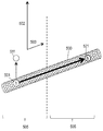
- FIG. 8 is a schematic diagram for explaining the movement of charges in the carbon nanotube.
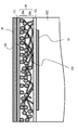
- FIG. 9 is a schematic cross-sectional view illustrating an example of the structure of the photoelectric conversion unit in the imaging apparatus according to the second embodiment.
- FIG. 10 is a schematic diagram illustrating the movement of charges in the photoelectric conversion unit of the imaging apparatus according to the second embodiment.
- An imaging device having sensitivity in the near-infrared region is required for use in an in-vehicle camera, a surveillance camera, or the like. For this reason, use of an organic semiconductor material having sensitivity in the near-infrared region as a photoelectric conversion material of a photoelectric conversion element has been studied.
- the inventor of the present application has focused on carbon nanotubes as a material having absorption in the near infrared region.
- Carbon nanotube molecules generally have a tube shape having a length of about several tens of nanometers to several millimeters, and have unique characteristics not found in various conventional organic and inorganic materials. In particular, it is known that the mobility of electrons and holes in the carbon nanotube is very large.
- the inventor of the present application has come up with a novel imaging device capable of high-speed operation using such characteristics of carbon nanotubes.
- summary of 1 aspect of this indication is as follows.
- An imaging apparatus including a plurality of pixels arranged in one or two dimensions, Each pixel is located between the electrode electrically connected between the plurality of pixels, a charge collection unit partitioned for each pixel, and between the electrode and the charge collection unit, A photoelectric conversion layer connected between pixels, the photoelectric conversion layer including a semiconductor-type carbon nanotube, a first substance having a larger electron affinity than the semiconductor-type carbon nanotube, and the semiconductor-type carbon nanotube.
- An imaging device comprising: a second substance having a small ionization potential. According to this configuration, an image pickup apparatus including a carbon nanotube as a photoelectric conversion material is actually obtained.
- the charge collection unit is an impurity diffusion region formed in the semiconductor substrate.
- Item 7 Item 5.
- the imaging device according to Item 4 wherein the charge collection unit is an electrode located on the semiconductor substrate.
- Item 8 Item 3.
- [Item 9] 4.
- the imaging apparatus according to item 2 further comprising a voltage supply circuit that is electrically connected to the electrode and generates a bias voltage determined so that a potential of the charge collection unit is lower than a potential of the electrode.
- An imaging apparatus including a plurality of pixels arranged one-dimensionally or two-dimensionally, wherein each pixel includes an electrode electrically connected between the plurality of pixels, and a charge collection unit partitioned for each pixel And one of a first substance having an electron affinity greater than that of the semiconductor-type carbon nanotube and a second substance having an ionization potential smaller than that of the semiconductor-type carbon nanotube,
- An imaging apparatus including a photoelectric conversion layer sandwiched between an electrode and the charge collection unit, wherein at least a part of the semiconductor-type carbon nanotube is electrically connected to the charge collection unit. According to this configuration, the pixel type electrode collects charges that move through the semiconductor carbon nanotubes, including the semiconductor carbon nanotubes with high carrier mobility.
- a stacked imaging apparatus can be realized.
- FIG. 1 illustrates an example of a circuit configuration of an imaging apparatus according to an embodiment of the present disclosure.
- An imaging apparatus 100 illustrated in FIG. 1 includes a plurality of unit pixel cells 20 and a peripheral circuit.
- the peripheral circuit includes a voltage supply circuit 10 that supplies a predetermined voltage to each of the unit pixel cells 20.
- the unit pixel cells 20 are arranged one-dimensionally or two-dimensionally on a semiconductor substrate to form a photosensitive region (pixel region).
- the unit pixel cells 20 are arranged in the row direction and the column direction.
- the row direction and the column direction mean directions in which the row and the column extend, respectively. That is, the vertical direction on the paper surface of FIG. 1 is the column direction, and the horizontal direction is the row direction.
- FIG. 1 shows four unit pixel cells 20 arranged in a 2 ⁇ 2 matrix.
- the number of unit pixel cells 20 shown in FIG. 1 is merely an example for explanation, and the number of unit pixel cells 20 is not limited to four.
- the imaging device 100 is a line sensor.
- Each unit pixel cell 20 includes a photoelectric conversion unit 30 and a signal detection circuit 40 that detects a signal generated by the photoelectric conversion unit 30.
- the photoelectric conversion unit 30 includes a pixel electrode (charge collecting unit) 32 and a counter electrode 38, and a photoelectric conversion layer 39 disposed therebetween.
- the counter electrode (electrode) 38 is connected to the voltage supply circuit 10 via the accumulation control line 22.
- a predetermined bias voltage is applied to the counter electrode 38 via the accumulation control line 22.
- the photoelectric conversion layer 39 includes semiconducting carbon nanotubes, and out of the hole-electron pairs generated by photoelectric conversion, the signal charge includes holes (positive charge) or electrons (negative charge). Either one is collected by the pixel electrode 32.
- the potential of the counter electrode 38 By controlling the potential of the counter electrode 38 using the bias voltage generated by the voltage supply circuit 10, either the hole or the electron can be collected by the pixel electrode 32.
- a voltage of about 10 V is applied to the accumulation control line 22 so that the potential of the counter electrode 38 is higher than that of the pixel electrode 32.
- the signal detection circuit 40 includes an amplification transistor (charge detection transistor) 42, an address transistor (row selection transistor) 44, and a reset transistor 46.
- the amplification transistor 42 and the address transistor 44 are field effect transistors (FETs) formed on a semiconductor substrate.
- FETs field effect transistors
- the “semiconductor substrate” in this specification is not limited to a substrate which is a semiconductor as a whole, and may be an insulating substrate provided with a semiconductor layer on the surface on which a photosensitive region is formed.
- An example of the semiconductor substrate is a p-type silicon substrate.
- one of the input terminal and output terminal of the amplification transistor 42 (typically the source) is connected to one of the input terminal and output terminal of the address transistor 44 (typically the drain).
- a control terminal (gate) of the amplification transistor 42 is electrically connected to the pixel electrode 32 of the photoelectric conversion unit 30.
- Signal charges (for example, holes) collected by the pixel electrode 32 are accumulated in a charge accumulation node (also referred to as a “floating diffusion node”) 41 between the pixel electrode 32 and the gate of the amplification transistor 42.
- a voltage corresponding to the signal charge stored in the charge storage node 41 is applied to the gate of the amplification transistor 42.
- the amplification transistor 42 amplifies this voltage. That is, the amplification transistor 42 amplifies the signal generated by the photoelectric conversion unit 30.
- the voltage amplified by the amplification transistor 42 is selectively read out via the address transistor 44 as a signal voltage.
- One of the source and the drain of the reset transistor 46 is connected to the charge storage node 41, and one of the source and the drain of the reset transistor 46 has an electrical connection with the pixel electrode 32.
- the reset transistor 46 resets the signal charge stored in the charge storage node 41. In other words, the reset transistor 46 resets the potential of the gate of the amplification transistor 42 and the pixel electrode 32.
- the imaging apparatus 100 includes a power supply line 23, a vertical signal line 24, an address signal line 25, and a reset signal line 26. These lines are connected to each unit pixel cell 20.
- the power supply line (source follower power supply) 23 is connected to one of the source and drain of the amplification transistor 42 and supplies a predetermined power supply voltage to each unit pixel cell 20.
- the vertical signal line 24 is connected to one of the source and drain of the address transistor 44 that is not connected to the source or drain of the amplification transistor 42.
- the address signal line 25 is connected to the gate electrode of the address transistor 44.
- the reset signal line 26 is connected to the gate of the reset transistor 46.
- the peripheral circuit of the imaging apparatus 100 includes a vertical scanning circuit (also referred to as “row scanning circuit”) 52, a horizontal signal readout circuit (also referred to as “column scanning circuit”) 54, and a plurality of column signal processing circuits (“row signal storage”). 56, also referred to as “circuit”, a plurality of load circuits 58, and a plurality of inverting amplifiers 59.
- the column signal processing circuit 56, the load circuit 58, and the inverting amplifier 59 are provided corresponding to each column of the plurality of unit pixel cells 20 arranged in the row direction and the column direction.
- Each of the column signal processing circuits 56 is electrically connected to the unit pixel cells 20 arranged in each column via the vertical signal line 24 corresponding to each column of the plurality of unit pixel cells 20.
- the plurality of column signal processing circuits 56 are electrically connected to the horizontal signal reading circuit 54.
- Each of the load circuits 58 is electrically connected to each vertical signal line 24, and a source follower circuit is formed by the load circuit 58 and the amplification transistor 42.
- the vertical scanning circuit 52 is connected to the address signal line 25 and the reset signal line 26.
- the vertical scanning circuit 52 applies a row selection signal for controlling on / off of the address transistor 44 to the gate of the address transistor 44 via the address signal line 25.
- By sending a row selection signal for each address signal line 25, the row to be read is scanned and selected.
- a signal voltage is read out from the unit pixel cell 20 of the selected row to the vertical signal line 24.
- the vertical scanning circuit 52 applies a reset signal for controlling on and off of the reset transistor 46 to the gate of the reset transistor 46 via the reset signal line 26.
- the vertical scanning circuit 52 selects the plurality of unit pixel cells 20 in units of rows, and reads out the signal voltage and resets the potential of the pixel electrode 32.
- the signal voltage read from the unit pixel cell 20 selected by the vertical scanning circuit 52 is sent to the column signal processing circuit 56 via the vertical signal line 24.
- the column signal processing circuit 56 performs noise suppression signal processing represented by correlated double sampling, analog-digital conversion (AD conversion), and the like.
- the horizontal signal reading circuit 54 sequentially reads signals from a plurality of column signal processing circuits 56 to a horizontal common signal line (not shown).
- the vertical scanning circuit 52 may include the voltage supply circuit 10 described above in part.
- the voltage supply circuit 10 may have an electrical connection with the vertical scanning circuit 52.
- a bias voltage may be applied to the counter electrode 38 via the vertical scanning circuit 52.
- a plurality of inverting amplifiers 59 are provided corresponding to each column.
- the negative input terminal of the inverting amplifier 59 is connected to the corresponding vertical signal line 24.
- the output terminal of the inverting amplifier 59 is connected to each unit pixel cell 20 in the corresponding column via a feedback line 27 provided corresponding to each column.
- the feedback line 27 is connected to the side (drain) of the source and drain of the reset transistor 46 that is not connected to the charge storage node 41. Therefore, the inverting amplifier 59 receives the output of the address transistor 44 at the negative terminal when the address transistor 44 and the reset transistor 46 are in a conductive state.
- a reset reference voltage is applied to the positive input terminal of the inverting amplifier 59 from a power source (not shown).
- the inverting amplifier 59 performs a feedback operation so that the gate voltage of the amplification transistor 42 becomes a predetermined feedback voltage.
- the feedback voltage means the output voltage of the inverting amplifier 59.
- the output voltage of the inverting amplifier 59 is, for example, 0V or a positive voltage near 0V.
- the inverting amplifier 59 may be called a “feedback amplifier”.
- FIG. 2 schematically illustrates a cross-section of the device structure of the unit pixel cell 20 in the imaging device 100 according to the embodiment of the present disclosure.
- the unit pixel cell 20 includes a semiconductor substrate 62 (for example, a silicon substrate) that supports the photoelectric conversion unit 30.
- the photoelectric conversion unit 30 is disposed above the semiconductor substrate 62.
- interlayer insulating layers 63A, 63B, and 63C are stacked on a semiconductor substrate 62, and a stacked body of a pixel electrode 32, a photoelectric conversion layer 39, and a counter electrode 38 is disposed on the interlayer insulating layer 63C. .
- the pixel electrode 32 is partitioned for each pixel, and the two adjacent pixel electrodes 32 are electrically separated by forming the pixel electrodes 32 spatially separated between the two adjacent unit pixel cells 20. It is separated.
- the photoelectric conversion layer 39 and the counter electrode 38 are formed so as to straddle the plurality of unit pixel cells 20.
- the counter electrode 38 is formed of, for example, a metal oxide such as ITO or ZnO, several layers of graphene, metal nanowires, or the like.
- an amplification transistor 42, an address transistor 44, and a reset transistor 46 are formed on the semiconductor substrate 62.
- the amplification transistor 42 includes impurity regions 62a and 62b formed in the semiconductor substrate 62, a gate insulating layer 42g located on the semiconductor substrate 62, and a gate electrode 42e located on the gate insulating layer 42g.
- the impurity regions (n-type impurity regions) 62a and 62b function as the drain or source of the amplification transistor 42.
- the address transistor 44 includes impurity regions 62a and 62c formed in the semiconductor substrate 62, a gate insulating layer 44g located on the semiconductor substrate 62, and a gate electrode 44e located on the gate insulating layer 44g.
- Impurity regions (n-type impurity regions) 62 a and 62 c function as the drain or source of address transistor 44.
- the amplification transistor 42 and the address transistor 44 share the impurity region 62a, so that the source (or drain) of the amplification transistor 42 and the drain (or source) of the address transistor 44 are electrically connected. .
- the reset transistor 46 includes impurity regions 62d and 62e formed in the semiconductor substrate 62, a gate insulating layer 46g located on the semiconductor substrate 62, and a gate electrode 46e located on the gate insulating layer 46g.
- the impurity regions (n-type impurity regions) 62d and 62e function as the drain or source of the reset transistor 46.
- element isolation regions 62s are provided between the unit pixel cells 20 adjacent to each other and between the amplification transistor 42 and the reset transistor 46.
- the unit pixel cells 20 adjacent to each other are electrically isolated by the element isolation region 62s. Further, by providing the element isolation region 62s between the unit pixel cells 20 adjacent to each other, leakage of signal charges accumulated in the charge accumulation node 41 is suppressed.
- a contact plug 65A connected to the impurity region 62d of the reset transistor 46, a contact plug 65B connected to the gate electrode 42e of the amplification transistor 42, and the contact plug 65A and the contact plug 65B are connected.
- a wiring 66A is formed.
- the n-type impurity region 62 d (for example, drain) of the reset transistor 46 is electrically connected to the gate electrode 42 e of the amplification transistor 42.
- a plug 67A and a wiring 68A are further formed in the interlayer insulating layer 63A.
- the plug 67B and the wiring 68B are formed in the interlayer insulating layer 63B, and the plug 67C is formed in the interlayer insulating layer 63C, whereby the wiring 66A and the pixel electrode 32 are electrically connected.
- Contact plug 65A, contact plug 65B, wiring 66A, plug 67A, wiring 68A, plug 67B, wiring 68B, and plug 67C are typically made of metal.
- a protective layer 72 is provided on the counter electrode 38.
- the protective layer 72 is not a substrate arranged to support the photoelectric conversion unit 30.
- microlenses may be disposed on the protective layer 72.
- FIG. 3A schematically shows a cross section of the photoelectric conversion unit 30 in the unit pixel cell 20.
- the photoelectric conversion unit 30 includes a counter electrode 38, a pixel electrode 32, and a photoelectric conversion layer 39.
- the photoelectric conversion layer 39 is sandwiched between the counter electrode 38 and the pixel electrode 32.
- the photoelectric conversion layer 39 is not separated for each pixel from the viewpoint of suppressing the occurrence of leakage current. That is, the photoelectric conversion layer 39 is formed across the plurality of unit pixel cells 20.
- the photoelectric conversion layer 39 includes a semiconductor-type carbon nanotube 105 and a charge separation material 106.
- the carbon nanotube has a structure in which a single-layer graphite sheet in which carbon atoms called graphene are arranged at the positions of hexagonal apexes is rounded into a cylindrical shape.
- Carbon nanotubes include single wall carbon nanotubes and multi-wall carbon nanotubes. In the imaging device of the present disclosure, either single-wall carbon nanotubes or multi-wall carbon nanotubes may be used. However, it is desirable to use single wall carbon nanotubes from the viewpoint of controlling the physical properties of the carbon nanotubes by chirality described below.
- the chirality By specifying chirality, the position of the carbon atom in the carbon nanotube is specified.
- Carbon nanotubes include those having metallic properties and those having semiconducting properties. Whether the carbon nanotube has a metallic property or a semiconducting property depends on chirality.
- semiconductor-type carbon nanotubes are used. That is, the carbon nanotube is not used as a mere electric conductor but is used for light detection, specifically, generation of a hole-electron pair by photoelectric conversion. It is desirable that the ratio of metal-type carbon nanotubes in the photoelectric conversion layer 39 is small. It is more desirable not to include metallic carbon nanotubes. This is because the generated hole-electron pairs disappear quickly in the metal-type carbon nanotube.
- Carrier mobility in semiconducting carbon nanotubes does not depend much on chirality.
- the hole mobility and the electron mobility of the semiconductor-type carbon nanotube are both tens of thousands cm 2 / Vs, which is 10 times faster than the electron mobility of silicon.
- the resonance wavelength of carbon nanotubes that is, the absorption wavelength depends on chirality. For this reason, the carbon nanotube absorption wavelength can be adjusted by changing the chirality.
- FIG. 5 shows the relationship between the chirality of the semiconductor-type carbon nanotube and the first and second resonance wavelengths.
- the first resonance wavelength is the longest wavelength at which resonance occurs
- the second resonance wavelength is the second longest wavelength at which resonance occurs.
- other wavelengths of resonance wavelengths may also exist in the semiconductor-type carbon nanotube.
- the wavelengths that can be absorbed resonantly are distributed from the visible region to the far infrared region.
- the resonance wavelength is distributed from the visible region to the near infrared region with a wavelength of about 1.6 ⁇ m.
- a semiconductor type carbon nanotube of chirality (8,0) has a resonance wavelength of about 780 nm.
- the chirality (7, 2) semiconductor-type carbon nanotube has a resonance wavelength of about 820 nm.
- an imaging apparatus capable of imaging blood oxygen concentration can be realized by using semiconductor carbon nanotubes having these chiralities for the photoelectric conversion layer.
- semiconductor-type carbon nanotubes such as chirality (12,4), (10,6), (13,0) resonately absorb near-infrared light of about 1.4 ⁇ m. This corresponds to the sun light missing wavelength region. Therefore, an imaging apparatus capable of taking an image without being affected by sunlight by using semiconductor carbon nanotubes having these chiralities for a photoelectric conversion layer and using illumination light having a wavelength of about 1.4 ⁇ m. It can be realized.
- the chirality (8,7) semiconducting carbon nanotube has a resonance wavelength of about 1.3 ⁇ m. This is a wavelength that is close to the sun light missing wavelength region but does not show much attenuation of sunlight. Therefore, by using semiconductor-type carbon nanotubes having these chiralities for the photoelectric conversion layer, it is possible to realize an imaging device capable of taking an image of sunlight in the vicinity of the sunlight-missing wavelength region.
- each semiconductor-type carbon nanotube has several resonance wavelengths, and there may be resonance wavelengths in the near infrared region and the visible region.
- the resonance of chirality (10,6) exists not only in the infrared region of about 1.4 ⁇ m but also in the visible region of about 750 nm. Therefore, an imaging apparatus capable of performing multispectral imaging is realized by using semiconductor carbon nanotubes having these chiralities for a photoelectric conversion layer and combining with an optical filter or the like.
- the photoelectric conversion layer 39 may include a semiconductor carbon nanotube 105 having a predetermined one chirality, or may include a semiconductor carbon nanotube 105 having two or more different chiralities. By including the semiconductor-type carbon nanotube 105 having two or more different chiralities, the wavelength band of light that can be detected by the imaging device can be expanded.
- Semiconductor carbon nanotubes having resonance wavelengths in the visible and near infrared regions have a diameter of about 1 nm.
- the charge separation material 106 has a semiconducting property or a semimetallic property.
- the charge separation material 106 pulls out one of the hole-electron pairs generated when the semiconductor-type carbon nanotube 105 receives light from the semiconductor-type carbon nanotube 105.
- the charge separation material 106 pulls out from the semiconductor-type carbon nanotube 105 the one not detected as a signal charge.
- the voltage supply circuit 10 supplies a bias voltage determined so that the potential of the pixel electrode 32 is lower than the potential of the counter electrode 38 to the counter electrode 38.
- a substance having an electron affinity larger than that of the semiconductor-type carbon nanotube 105 can be used as the charge separation material 106.
- the electron affinity is defined as an energy difference from the bottom of the conduction band 110 to the vacuum level 113 in the semiconductor.
- the electron affinity is an energy difference between the LUMO level and the vacuum level. More generally, it is the maximum value of the energy difference between the energy level and the vacuum level at which an excess of one electron can be received in the neutral state.
- the charge separation material 106 is a substance having an electron affinity greater than that of the semiconductor-type carbon nanotube 105, among the hole-electron pairs generated in the semiconductor-type carbon nanotube 105, the electrons are charge-separated at a lower energy level. The material 106 moves to the conduction band 110. For this reason, holes remain in the valence band 111 of the semiconductor-type carbon nanotube 105.
- the electron affinity of semiconducting carbon nanotubes having resonance wavelengths in the visible and near infrared regions is approximately 3 eV to 4 eV.
- fullerenes and fullerene derivatives can be cited as substances having an electron affinity greater than that of the semiconductor-type carbon nanotube 105.
- Fullerenes and fullerene derivatives are referred to as molecules having a fullerene skeleton.
- C60 has an electron affinity of about 4 eV.
- C70, C80, phenyl C61 butyric acid methyl ester (PCBM), indene C60 bis-adduct (ICBA), indene C60 mono-adduct (ICMA) and the like in which these fullerene skeletons are introduced are also 3.7 eV. Has an electron affinity of about 3.8 eV.
- the voltage supply circuit 10 supplies the counter electrode 38 with a bias voltage determined so that the potential of the pixel electrode 32 is higher than the potential of the counter electrode 38.
- a substance having an ionization potential smaller than that of the semiconductor-type carbon nanotube 105 can be used as the charge separation material 106.
- the ionization potential is defined as an energy difference from the bottom of the valence band 111 to the vacuum level 113 in the semiconductor.
- the ionization potential is an energy difference between the HOMO level and the vacuum level. More generally, it is the minimum value of energy required to lift one electron from the neutral state to the vacuum level.
- the charge separation material 106 is a substance having an ionization potential smaller than that of the semiconductor-type carbon nanotube 105, the charge-separation material 106 becomes more stable when it becomes a positive ion. In the pair, holes move to the valence band 111 of the charge separation material 106. For this reason, electrons remain in the conduction band 110 of the semiconductor-type carbon nanotube 105.
- the ionization potential of semiconducting carbon nanotubes having resonance wavelengths in the visible and near infrared regions is approximately 4 eV to 5 eV.
- substances having an ionization potential smaller than that of the semiconductor carbon nanotube 105 include poly (3-dodecylthiophene-2,5-diyl) (P3DDT, ionization potential: about 4.6 eV), poly (3-hexylthiophene-2) , 5-diyl) (P3HT, ionization potential: about 5 eV).
- the electron affinity and ionization potential of the semiconductor carbon nanotube 105 also differ depending on the chirality. For this reason, it is desirable to calculate the electron affinity and ionization potential of the semiconductor-type carbon nanotube 105 in consideration of chirality, and to select the charge separation material 106 so as to satisfy the above-described relationship.
- the semiconductor carbon nanotube 105 and the charge separation material 106 may be dispersed with each other.
- the distribution of the semiconductor-type carbon nanotube 105 and the charge separation material 106 may not be uniform.
- the distribution may be biased in the thickness direction of the photoelectric conversion layer 39.
- the signal charge can move from the semiconductor-type carbon nanotube 105 to the pixel electrode 32.
- the semiconductor carbon nanotube 105 and the pixel electrode 32 are electrically connected.
- a part of the semiconductor-type carbon nanotube 105 may be in direct contact with the pixel electrode 32.
- the photoelectric conversion unit 30 may further include a hole blocking layer 103 and an electron blocking layer 101. These layers are arranged at positions where movement of holes and electrons is desired to be suppressed. For example, when the pixel electrode 32 collects electrons, the hole blocking layer 103 is provided between the pixel electrode 32 and the photoelectric conversion layer 39, and the electron blocking layer 101 is opposed to the counter electrode 38 and the photoelectric conversion layer 39. Between.
- the hole blocking layer 103 transports negative charges generated in the photoelectric conversion layer 39 to the pixel electrode 32, and prevents positive charges from entering the photoelectric conversion layer 39 from the pixel electrode 32. It is desirable to provide the hole blocking layer 103 in order to suppress a current that flows even in a state where no light is irradiated, so-called dark current.
- batocuproine BCP
- BCP batocuproine
- the electron block layer 101 plays a role of transporting positive charges generated in the photoelectric conversion layer 39 to the counter electrode 38 and also prevents negative charges from entering the photoelectric conversion layer 39 from the counter electrode 38. In order to suppress the dark current, it is desirable to provide the electron block layer 101.
- poly (3,4-ethylenedioxythiophene) -poly (styrene sulfonate) PEDOT / PSS
- PEDOT / PSS poly (3,4-ethylenedioxythiophene) -poly (styrene sulfonate)
- the hole blocking layer 103 and the electron blocking layer 101 have electrical conductivity in order to transport electrons (negative charge) and holes (positive charge), respectively. Therefore, when the hole blocking layer 103 is provided between the pixel electrode 32 and the photoelectric conversion layer 39, a part of the semiconductor carbon nanotube 105 is in contact with the hole blocking layer 103, so that the semiconductor carbon nanotube 105 A part is electrically connected to the pixel electrode 32 through the hole blocking layer 103. In addition, even when the electron blocking layer 101 is provided between the pixel electrode 32 and the photoelectric conversion layer 39, a part of the semiconductor carbon nanotube 105 is in contact with the electron blocking layer 101 by a part of the semiconductor carbon nanotube 105. Are electrically connected to the pixel electrode 32 through the electron block layer 101.
- the hole blocking layer 103 When the hole blocking layer 103 is used between the photoelectric conversion layer 39 and the pixel electrode 32, between the semiconductor-type carbon nanotube 105 and the hole blocking layer 103 and between the hole blocking layer 103 and the pixel electrode 32. It suffices if the signal charge can move between the two. A part of the semiconductor-type carbon nanotube 105 may be in direct contact with the hole blocking layer 103.
- the semiconductor carbon nanotube 105 and the pixel electrode 32 or the hole blocking layer 103 may not be in direct contact. This is because the signal charge can move through another charge transport material or by a tunnel phenomenon. However, the charge transport due to these other charge transport materials and the tunnel phenomenon is generally slower than the charge transport in the semiconductor-type carbon nanotube 105. Therefore, it is desirable that a part of the semiconductor-type carbon nanotube 105 is directly in contact with the pixel electrode 32 or the hole blocking layer 103 as much as possible, or is distributed to the vicinity of the pixel electrode 32 or the hole blocking layer 103 as much as possible. .
- the electron blocking layer 101 is used between the photoelectric conversion layer 39 and the pixel electrode 32. In that case, by replacing all the hole blocking layers 103 with the electron blocking layers 101, the arrangement of the semiconductor-type carbon nanotubes 105 is similarly explained.
- the density of the semiconductor carbon nanotubes 105 in the thickness direction of the photoelectric conversion layer 39 may be low on the counter electrode 38 side and high on the pixel electrode 32 side.
- the density of the charge separation material 106 in the thickness direction of the photoelectric conversion layer 39 is desirably high on the counter electrode 38 side and low on the pixel electrode 32 side.
- the photoelectric conversion layer 39 may include a layer 39a including only the charge separation material 106 and a layer 39b including only the semiconductor-type carbon nanotube 105.
- the layer 39 b including only the semiconductor-type carbon nanotube 105 is in contact with the pixel electrode 32
- the layer 39 a including only the charge separation material 106 is in contact with the counter electrode 38.
- the thickness of the photoelectric conversion layer 39 is, for example, several tens nm to several hundreds nm.
- the photoelectric conversion layer 39 may further include an n-type semiconductor or a p-type semiconductor.
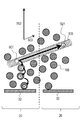
- FIG. 7 is a schematic diagram showing the positional relationship between the semiconductor-type carbon nanotube 105 and the charge separation material 106 in the photoelectric conversion layer 39, the pixel electrode 32, and the counter electrode 38.
- FIG. 7 only the semiconductor carbon nanotube 105 and the charge separation material 106 of interest are shown by solid lines. In the following example, electrons are used as signal charges.
- the charge separation material 106 is a substance having an ionization potential smaller than that of the semiconductor carbon nanotube 105.
- the bias voltage is supplied to the counter electrode 38 so that the potential of the pixel electrode 32 is higher than the potential of the counter electrode 38. For this reason, an electric field is generated in the direction indicated by the arrow 502.
- the exciton charge is separated. Specifically, since the charge separation material 106 has a smaller ionization potential than the semiconductor-type carbon nanotube 105, the charge-separation material 106 receives the positive charge h rather than the semiconductor-type carbon nanotube 105 continues to hold the positive charge h. Is more energetically stable. For this reason, the positive charge h is extracted by the charge separation material 106. As a result, the positive charge moves to one molecule of the charge separation material 106, and the negative charge e remains in the semiconductor-type carbon nanotube 105.
- the charge separation occurs at a position where the semiconductor carbon nanotube 105 and the charge separation material 106 are close to each other. For this reason, if one or more molecules of the charge separation material 106 exist in the unit pixel cell 20 around one semiconductor-type carbon nanotube 105 molecule, charge separation occurs in the pixel in which the excitons are generated. . In order to generate excitons and charge separation in the same unit pixel cell, the ratio of the charge separation material 106 contained in the photoelectric conversion layer 39 may be increased.
- the negative charge e remaining in the semiconductor-type carbon nanotube 105 and the positive charge h transferred to the charge separation material 106 are not neutral even macroscopically. Therefore, the negative charge e and the positive charge h are affected by the electric field indicated by the arrow 502 due to the voltage applied between the counter electrode 38 and the pixel electrode 32 and start moving.
- the negative charge e remaining in the semiconductor-type carbon nanotube 105 is affected by the electric field indicated by the arrow 502 and moves in the semiconductor-type carbon nanotube 105 to the pixel electrode 32 side. This movement is very fast. As indicated by an arrow 504, the negative charge e moves to a position where the semiconductor carbon nanotube 105 is in contact with the pixel electrode 32 and is collected by the pixel electrode 32. That is, in the imaging device of the present disclosure, the charge generated by photoelectric conversion is detected in a very short time.
- the positive charge h that has moved to one molecule of the charge separation material 106 moves to the molecule of the adjacent charge separation material 106 by hopping conduction.
- Which molecule is hopped is determined by the distance between the molecules, the direction and intensity of the electric field. If the intermolecular distance is approximately equal, a molecule in a direction closer to the direction parallel to the electric field is selected as the hopping destination. When the strength of the electric field is large, the probability that a molecule in a direction closer to the direction parallel to the electric field is selected as a hopping destination increases even if there is a difference in intermolecular distance.
- the positive charge h is macroscopically indicated by an arrow 503. It moves in the direction of the electric field and is collected by the counter electrode 38.
- the case where the distribution of the intermolecular distance is extremely biased is, for example, the case where the molecules of the charge separation material 106 are arranged only in a certain plane.
- the carrier mobility in the charge separation material 106 is generally much smaller than that of semiconductor carbon nanotubes. Further, the movement of the positive charge h between the molecules of the charge separation material 106 by hopping is slower than the movement of carriers in the semiconductor-type carbon nanotube 105.
- FIG. 7 shows an example in which the negative charge e is directly collected by the pixel electrode 32 from the molecule of the semiconductor carbon nanotube 105 in which excitons are generated.
- the molecules of the semiconductor-type carbon nanotube 105 do not have to be in direct contact with the pixel electrode 32.
- the charge of the semiconductor-type carbon nanotube 105 that is not in direct contact with the pixel electrode 32 moves as follows. First, hopping moves to another semiconductor carbon nanotube 105 that is in close proximity or in contact therewith. By repeating this, charges move to the semiconductor carbon nanotube 105 that is in direct contact with the pixel electrode 32. Finally, charges are collected in the pixel electrode 32 from the semiconductor carbon nanotube 105 that is in direct contact with the pixel electrode 32.
- the photoelectric conversion layer 39 contains the charge separation material 106
- one of the hole-electron pairs can be extracted from the semiconductor carbon nanotube 105.
- the electric charge remaining in the carbon nanotubes 105 moves between the semiconductor-type carbon nanotubes 105 at a high speed and can be collected by the electrode 32.
- the imaging device according to the present disclosure can exhibit the above-described effects according to the content of the charge separation material 106 in the photoelectric conversion layer 39.
- the imaging apparatus of the present embodiment the charge that moves through the semiconductor carbon nanotube including the semiconductor carbon nanotube with high carrier mobility is collected by the pixel electrode. For this reason, it is possible to realize an imaging device capable of shooting at a high speed and a high frame rate. For example, a distance image (Time-of-Flight) image sensor can be realized.
- carbon nanotubes have high chemical stability and are difficult to deteriorate in characteristics. Therefore, an imaging device that can be used in a wide temperature range and has high durability and reliability can be realized.
- the imaging device 100 can be manufactured using a general semiconductor manufacturing process.
- the imaging device 100 can be manufactured by using various silicon semiconductor processes.
- an amplification transistor 42, an address transistor 44, and a reset transistor 46 are formed on a semiconductor substrate 62 using various semiconductor manufacturing techniques. Thereafter, interlayer insulating layers 63A to 63C, contact plugs 65A and 65B, wirings 66A, 68A and 68B, plugs 67A to 67C and pixel electrode 32 are formed.
- the hole blocking layer 103 is formed on the interlayer insulating layer 63C provided with the pixel electrode 32.
- the hole blocking layer 103 is formed by vapor deposition.
- the hole blocking layer 103 is formed using a material soluble in a solvent, a spin coating method, an ink jet method, or the like can be used.
- the photoelectric conversion layer 39 includes a semiconductor-type carbon nanotube 105 and a charge separation material 106.
- the semiconductor-type carbon nanotube 105 and the charge separation material 106 are prepared, mixed in a solvent, and deposited on the interlayer insulating layer 63C by spin coating, doctor blade, or ink jet coating. Alternatively, they may be dispersed in different solvents and applied onto the interlayer insulating layer 63C by applying each of them.
- the semiconductor-type carbon nanotube 105 may be attached on the interlayer insulating layer 63C by coating, and the charge separation material 106 may be formed on the interlayer insulating layer 63C by vapor deposition.
- the charge-separation material 106 and the semiconductor-type are so arranged that the semiconductor-type carbon nanotube 105 and the charge separation material 106 are dispersed with each other.
- the carbon nanotubes 105 may be alternately arranged on the interlayer insulating layer 63C, and any one of the arrangements may be performed at least twice.
- solubilizer In order to disperse the semiconductor-type carbon nanotube 105 in a solvent, a polymer or a surfactant may be used as a solubilizer. These solubilizers may remain in the photoelectric conversion layer 39 as long as they do not adversely affect the characteristics of the image sensor. Alternatively, only the solubilizer may be removed after the coating step.
- the semiconducting carbon nanotube 105 can be obtained by sorting out semiconducting carbon nanotubes from mass produced carbon nanotubes.
- Examples of methods for producing semiconductor-type carbon nanotubes include HiPCO method, CoMoCAT method, alcohol CVD method, and arc discharge method. Or you may utilize, after performing chirality selection operation so that the composition ratio of desirable chirality may increase.
- These semiconductor type selection and chirality selection methods are, for example, (1) T.W. Tanaka et al., Applied Physics Express 2008, VOL. 1, 11001 pages, (2) H.P. Liu et al., Nature Communications 2011, DOI: 10.1038 / ncomms1313, (3) A. Nishi et al., Nature Technology 2007, VOL. 2, pages 640-646.
- a large area coating technique such as spin coating or doctor blade method can be used.
- the following method can be used when manufacturing an imaging device having different spectral sensitivity characteristics for each pixel.
- a dispersion liquid in which semiconductor carbon nanotubes having one or two or more chiralities are dispersed is prepared.
- each dispersion liquid is selectively discharged by an ink jet method. Accordingly, the photoelectric conversion layer 39 having different spectral sensitivity characteristics for each pixel can be formed without using a mask.
- the photoelectric conversion layer 39 having different spectral sensitivity characteristics for each pixel may be formed by using a spin coat, a doctor blade method, and the like together with a mask.
- a semiconductor-type carbon nanotube having a high chirality (8, 0) ratio can be used as the first pixel
- a semiconductor-type carbon nanotube having a high chirality (7, 2) ratio can be used as the second pixel.
- the first pixel has higher sensitivity to light having a wavelength of 780 nm than the second pixel
- the second pixel has higher sensitivity to light having a wavelength of 820 nm than the first pixel. Therefore, if the respective images composed of these two types of pixels are compared, the redox degree of hemoglobin can be imaged.
- a semiconductor type carbon nanotube having a high ratio such as chirality (12, 4), (10, 6), (13, 0) is used as the first pixel, and chirality (8, 7) is used as the second pixel. It is also possible to use semiconducting carbon nanotubes. In this case, it is possible to obtain an image at the sun light missing wavelength and the wavelength that is not missing in the vicinity thereof.
- the charge separation material 106 for example, a commercially available material can be used. Or you may arrange
- the electron blocking layer 101 is formed on the photoelectric conversion layer 39 by the same method as the hole blocking layer 103.
- the counter electrode 38 is formed.
- ITO is formed by sputtering.
- the protective layer 72 and the microlens 74 the imaging device is completed.
- the photoelectric conversion unit 30 can be manufactured without using the crystallinity of the surface of the support that supports the photoelectric conversion unit 30.
- the formation of the photoelectric conversion unit 30 does not include a process that requires processing at a high temperature. Therefore, it can be stacked with a semiconductor substrate provided with a signal detection circuit, and a stacked imaging device can be realized.
- the second embodiment is different from the first embodiment in that the charge separation material extracts the signal charge from the hole-charge pair generated in the carbon nanotube. First, the inventors' knowledge will be described.
- Carbon nanotubes generally have a length of about several tens of nanometers to several millimeters.
- the thickness of the photoelectric conversion layer of the photoelectric conversion element is generally several nm to several hundred nm. For this reason, when a carbon nanotube is used for a photoelectric conversion element as a photoelectric conversion material, the component of the carbon nanotube arranged in parallel to the photoelectric conversion layer (direction perpendicular to the thickness direction) is thicker in the photoelectric conversion layer. It becomes longer than the component arranged in the vertical direction.
- FIG. 8 schematically shows the carbon nanotube 500 positioned in the photoelectric conversion layer.
- a positive charge h exists at the position 501 of the carbon nanotube 500, and an electric field is applied from the outside in the direction of the arrow 502.
- the charge h moves to the position 511 moved in parallel along the arrow 502.
- the electric field indicated by the arrow 502 has an electric field component in the longitudinal direction 503 of the carbon nanotube 500. It is known that the charge transfer along the longitudinal direction in the carbon nanotube 500 hardly receives resistance, and the mobility in this direction is reported to be 10,000 cm 2 / (V ⁇ s) or more. . For this reason, as long as the component parallel to the longitudinal direction of the carbon nanotube 500 in the electric field is not zero, the charge h easily moves in the carbon nanotube 500 and moves to the position 521.
- the imaging device is composed of a plurality of pixels, and forms an image by generating a signal proportional to the amount of light incident on each pixel.
- carbon nanotubes are used for the photoelectric conversion layer, charges generated by photoelectric conversion move in the carbon nanotubes for the reasons described above. For this reason, when the length of the carbon nanotube is larger than the size of the pixel 505 and the charge generated by photoelectric conversion moves in the carbon nanotube, the pixel on which the light is incident and the incident light are detected. The pixel may be different. Even when the length of the carbon nanotube is smaller than the size of the pixel 505, the same applies to the case where the carbon nanotube is located across two pixels. As a result, crosstalk of detection signals between pixels occurs, and the obtained image does not correctly reflect the original light irradiation amount distribution and may be blurred.
- the imaging apparatus of the present embodiment solves this problem, and is particularly suitable for an imaging apparatus with a narrow pixel pitch.
- the overall configuration of the imaging apparatus of the present embodiment is the same as, for example, the imaging apparatus of the first embodiment shown in FIG.
- the device structure of the imaging apparatus of the present embodiment is the same as that of the imaging apparatus of the first embodiment shown in FIG. 2, for example.
- FIG. 9 schematically shows a cross section of the photoelectric conversion unit 30 extending over a plurality of unit pixel cells 20.
- the photoelectric conversion unit 30 includes a counter electrode 38, a pixel electrode 32, and a photoelectric conversion layer 39.
- the photoelectric conversion layer 39 is sandwiched between the counter electrode 38 and the pixel electrode 32.
- the photoelectric conversion layer 39 is not separated for each pixel from the viewpoint of suppressing the occurrence of leakage current, and is formed across a plurality of unit pixel cells 20.
- the photoelectric conversion layer 39 includes a semiconductor-type carbon nanotube 105 and a charge separation material 106. At least a part of the carbon nanotube 10 is located across the plurality of unit pixel cells 20.
- the structure and physical properties of the carbon nanotube 105 are as described in the first embodiment.
- the charge separation material 106 may be the material described in the first embodiment. That is, the charge separation material 106 may be a substance having a larger electron affinity than the semiconductor carbon nanotube 105 or a substance having an ionization potential smaller than that of the semiconductor carbon nanotube 105.
- the charge extracted from the carbon nanotube by the charge separation material is used as the pixel electrode.
- the voltage supply circuit 10 supplies a bias voltage to the counter electrode 38 so that the potential of the pixel electrode 32 is higher than the potential of the counter electrode 38.
- a substance having an electron affinity higher than that of the semiconductor-type carbon nanotube 105 can be used as the charge separation material 106.
- the voltage supply circuit supplies a bias voltage to the counter electrode 38 so that the potential of the pixel electrode 32 is lower than the potential of the counter electrode 38.
- a substance having an ionization potential smaller than that of the semiconductor-type carbon nanotube 105 can be used as the charge separation material 106.
- the charge separation material 106 becomes more stable when it becomes positive ions, holes move out of the hole-electron pairs generated in the semiconductor-type carbon nanotube 105 to the valence band of the charge separation material 106.
- the charge separation material 106 does not have one-dimensional charge transfer inside.
- the charge is limited by molecular orbitals.
- a charge bias occurs in the molecule, but a charge transfer that forms a macroscopic current does not occur. That is, there is no macroscopic charge transfer freedom inside.
- the internal charge transfer is zero-dimensional.
- many conductive polymers have a one-dimensional chain-like molecular shape due to covalent bonds, and have a structure in which these are complicatedly entangled.
- the semiconductor-type carbon nanotube 105 and the charge separation material 106 are dispersed with each other. As long as they are mutually dispersed, the distribution of the semiconductor-type carbon nanotubes 105 and the charge separation material 106 may not be uniform. For example, the distribution may be biased in the thickness direction of the photoelectric conversion layer 39. Specifically, unlike the first embodiment, the density of the semiconductor carbon nanotubes 105 in the thickness direction of the photoelectric conversion layer 39 may be high on the counter electrode 38 side and low on the pixel electrode 32 side. Further, the density of the charge separation material 106 in the thickness direction of the photoelectric conversion layer 39 may be low on the counter electrode 38 side and high on the pixel electrode 32 side.
- the thickness of the photoelectric conversion layer 39 is, for example, several tens nm to several hundreds nm.
- the photoelectric conversion layer 39 may further include an n-type semiconductor or a p-type semiconductor.
- the photoelectric conversion unit 30 may further include a hole blocking layer 103 and an electron blocking layer 101.
- the materials described in the first embodiment can be used for the hole blocking layer 103 and the electron blocking layer 101.
- FIG. 10 is a schematic diagram showing the positional relationship between the arrangement of the semiconductor carbon nanotube 105 and the charge separation material 106 located in the photoelectric conversion layer 39 and the pixel electrode 32 of the unit pixel cell.
- the semiconductor-type carbon nanotube 105 is located across the two unit pixel cells 20.
- electrons are used as signal charges as in the first embodiment, but unlike the first embodiment, the charge separation material 106 is a substance having a higher electron affinity than the semiconductor carbon nanotube 105. It is.
- the bias voltage is supplied to the counter electrode 38 so that the potential of the pixel electrode 32 is higher than the potential of the counter electrode 38. For this reason, an electric field is generated in the direction indicated by the arrow 502.
- the exciton charge is separated. Specifically, the negative charge e is extracted by the charge separation material 106, one charge moves to one molecule of the charge separation material 106, and the other charge remains in the semiconductor-type carbon nanotube 105.
- the charge separation material 106 has a larger electron affinity than the semiconductor-type carbon nanotube 105, so that the negative charge e is extracted. As a result, a positive charge remains in the semiconductor carbon nanotube 105.
- the charge separation occurs at a position where the semiconductor carbon nanotube 105 and the charge separation material 106 are close to each other. For this reason, if one or more molecules of the charge separation material 106 exist in the unit pixel cell 20 around one semiconductor-type carbon nanotube 105 molecule, charge separation occurs in the pixel in which the excitons are generated. . In order to generate excitons and charge separation in the same unit pixel cell, the ratio of the charge separation material 106 contained in the photoelectric conversion layer 39 may be increased.
- the positive charge h remaining on the semiconductor-type carbon nanotube 105 and the negative charge e transferred to the charge separation material 106 are not neutral even macroscopically. Therefore, the positive charge h and the negative charge e are affected by the electric field indicated by the arrow 502 due to the voltage applied between the counter electrode 38 and the pixel electrode 32 and start moving.
- the positive charge h remaining in the semiconductor-type carbon nanotube 105 is strongly influenced not only by the direction of the arrow 502 but also by the electric field component along the direction 503 in which the semiconductor-type carbon nanotube 105 extends due to the anisotropy of electric conduction of the carbon nanotube. Move. As a result, the positive charge h moves in the extending direction of the semiconductor carbon nanotube 105 and reaches the position 521. This positive charge h is collected by the counter electrode 38 (not shown). Since the counter electrode 38 is formed across a plurality of pixels, the positive charge h may be collected at any position.
- the negative charge e that has moved to one molecule of the charge separation material 106 moves to the molecule of the adjacent charge separation material 106 by hopping conduction.
- Which molecule is hopped is determined by the distance between the molecules, the direction and intensity of the electric field. If the intermolecular distance is approximately equal, a molecule in a direction closer to the direction parallel to the electric field is selected as the hopping destination. In addition, when the electric field strength is high, the probability that a molecule in a direction closer to the direction parallel to the electric field is selected as a hopping destination even if there is a difference in intermolecular distance.
- the distribution of the intermolecular distance of the charge separation material 106 is not extremely biased and is distributed three-dimensionally in the photoelectric conversion layer 39, the negative charge e moves macroscopically in the direction of the electric field.
- the case where the distribution of the intermolecular distance is extremely biased is, for example, the case where the molecules of the charge separation material 106 are arranged only in a certain plane.
- excitons are collected by the pixel electrode 32 in the unit pixel cell 20. That is, the pixel on which the light is incident matches the pixel that detects the incident light.
- 10 shows one semiconductor-type carbon nanotube 105, but in the photoelectric conversion layer 39, two or more semiconductor-type carbon nanotubes 105 can be close to each other.
- charge separation between the semiconductor-type carbon nanotube 105 and the charge separation material 106 and charge transfer between molecules of the charge separation material 106 in addition to (i) charge separation between the semiconductor-type carbon nanotube 105 and the charge separation material 106 and (ii) charge transfer between molecules of the charge separation material 106, (iii) 2 Charge separation between the semiconductor-type carbon nanotubes 105 as described above, and (iV) charge transfer from the semiconductor-type carbon nanotubes 105 to the charge separation material 106 may occur.
- the electron affinity and the ionization potential are equal between the semiconductor carbon nanotubes 105 having the same chirality. From the viewpoint of electron affinity or ionization potential, it is energetically advantageous for positive or negative charges to be detected as signals to move from the semiconductor-type carbon nanotube 105 to the charge separation material 106. Therefore, it is difficult for positive charges or negative charges to move from the charge separation material 106 to the semiconductor-type carbon nanotube 105. For this reason, the movement of charges shown in (iii) and (iV) is energetically disadvantageous compared to (i) and (ii) and is unlikely to occur.
- the photoelectric conversion layer 39 includes the charge separation material 106 as much as possible, the charge to be detected as a signal in the semiconductor carbon nanotube 105 is transferred from the semiconductor carbon nanotube 105.
- the electric charge to be detected as a signal can be moved toward the pixel electrode 32 according to the electric field generated by the extraction and the voltage applied between the counter electrode 38 and the pixel electrode 32.
- the imaging device according to the present disclosure can exhibit the above-described effects according to the content of the charge separation material 106 in the photoelectric conversion layer 39.
- an imaging device that can suppress detection charge mixing between pixels and obtain a high-definition image, or a minute pixel A size imaging device can be realized.
- the imaging device of the present embodiment can be manufactured using a general semiconductor manufacturing process, like the imaging device of the first embodiment.
- the imaging device can be manufactured by using various silicon semiconductor processes.
- each of the amplification transistor 42, the address transistor 44, and the reset transistor 46 is an N-channel MOS.
- the transistors in the embodiments of the present disclosure are not limited to N-channel MOS.
- the amplification transistor 42, address transistor 44, and reset transistor 46 may be P-channel MOS. Further, it is not necessary that all of these are unified as either the N channel MOS or the P channel MOS.
- a bipolar transistor can be used in addition to the FET.
- the image pickup apparatus having a form for collecting the charges to be detected by the pixel electrode has been described.
- the imaging device includes an impurity diffusion region provided in the semiconductor substrate instead of the pixel electrode, and the impurity diffusion region collects one of the hole-electron pairs generated in the photoelectric conversion layer as a charge to be detected. Also good.
- the imaging device of the present disclosure can be suitably used for various imaging devices that can acquire images in the visible region and the near-infrared region.
- it can be suitably used for an imaging device with a high speed operation, a high frame rate and / or an imaging device with a high definition and a high number of pixels, and an imaging device with a minute pixel size.
Landscapes
- Engineering & Computer Science (AREA)
- Chemical & Material Sciences (AREA)
- Materials Engineering (AREA)
- Nanotechnology (AREA)
- Physics & Mathematics (AREA)
- Electromagnetism (AREA)
- Multimedia (AREA)
- Signal Processing (AREA)
- Solid State Image Pick-Up Elements (AREA)
- Light Receiving Elements (AREA)
- Transforming Light Signals Into Electric Signals (AREA)
- Color Television Image Signal Generators (AREA)
Abstract
Ce dispositif d'imagerie comprend une pluralité de pixels agencés de manière unidimensionnelle ou bidimensionnelle. Chacun des pixels (20) comprend : une électrode (38) permettant d'établir des connexions électriques parmi la pluralité de pixels; une partie de collecte de charge (32) compartimentée pour chaque pixel; et une couche de conversion photoélectrique (39) connectée parmi la pluralité de pixels et située entre l'électrode et la partie de collecte de charge. La couche de conversion photoélectrique comprend : un nanotube de carbone de type semi-conducteur (105); et une substance parmi une première substance (106) ayant une plus grande affinité électronique que le nanotube de carbone de type semi-conducteur, et une seconde substance (106) ayant un plus petit potentiel d'ionisation que le nanotube de carbone de type semi-conducteur.
Priority Applications (10)
| Application Number | Priority Date | Filing Date | Title |
|---|---|---|---|
| EP16821000.3A EP3321964B1 (fr) | 2015-07-08 | 2016-06-17 | Dispositif d'imagerie |
| CN202210219777.1A CN114582922A (zh) | 2015-07-08 | 2016-06-17 | 摄像装置 |
| EP19188129.1A EP3582264B1 (fr) | 2015-07-08 | 2016-06-17 | Dispositif d'imagerie |
| JP2017513152A JP6161018B2 (ja) | 2015-07-08 | 2016-06-17 | 撮像装置 |
| CN201680007083.4A CN107210312B (zh) | 2015-07-08 | 2016-06-17 | 摄像装置 |
| CN202210219708.0A CN114582906B (zh) | 2015-07-08 | 2016-06-17 | 摄像装置及利用该摄像装置的方法 |
| EP20192168.1A EP3767674B1 (fr) | 2015-07-08 | 2016-06-17 | Dispositif d'imagerie |
| US15/729,739 US10672836B2 (en) | 2015-07-08 | 2017-10-11 | Imaging device |
| US16/831,231 US11094746B2 (en) | 2015-07-08 | 2020-03-26 | Imaging device |
| US17/364,493 US11793008B2 (en) | 2015-07-08 | 2021-06-30 | Imaging device |
Applications Claiming Priority (6)
| Application Number | Priority Date | Filing Date | Title |
|---|---|---|---|
| JP2015137064 | 2015-07-08 | ||
| JP2015-137063 | 2015-07-08 | ||
| JP2015137063 | 2015-07-08 | ||
| JP2015-137064 | 2015-07-08 | ||
| JP2016-082890 | 2016-04-18 | ||
| JP2016082890 | 2016-04-18 |
Related Child Applications (1)
| Application Number | Title | Priority Date | Filing Date |
|---|---|---|---|
| US15/729,739 Continuation US10672836B2 (en) | 2015-07-08 | 2017-10-11 | Imaging device |
Publications (1)
| Publication Number | Publication Date |
|---|---|
| WO2017006520A1 true WO2017006520A1 (fr) | 2017-01-12 |
Family
ID=57685347
Family Applications (1)
| Application Number | Title | Priority Date | Filing Date |
|---|---|---|---|
| PCT/JP2016/002917 Ceased WO2017006520A1 (fr) | 2015-07-08 | 2016-06-17 | Dispositif d'imagerie |
Country Status (5)
| Country | Link |
|---|---|
| US (3) | US10672836B2 (fr) |
| EP (3) | EP3582264B1 (fr) |
| JP (3) | JP6161018B2 (fr) |
| CN (3) | CN107210312B (fr) |
| WO (1) | WO2017006520A1 (fr) |
Cited By (9)
| Publication number | Priority date | Publication date | Assignee | Title |
|---|---|---|---|---|
| JP2018195809A (ja) * | 2017-05-15 | 2018-12-06 | パナソニックIpマネジメント株式会社 | 光電変換素子の製造方法 |
| WO2020105360A1 (fr) * | 2018-11-19 | 2020-05-28 | パナソニックIpマネジメント株式会社 | Capteur optique et système de détection optique |
| WO2020209002A1 (fr) * | 2019-04-10 | 2020-10-15 | パナソニックIpマネジメント株式会社 | Dispositif d'imagerie |
| WO2021176876A1 (fr) * | 2020-03-05 | 2021-09-10 | パナソニックIpマネジメント株式会社 | Capteur d'image et système d'imagerie |
| JPWO2022244575A1 (fr) * | 2021-05-21 | 2022-11-24 | ||
| WO2022249844A1 (fr) * | 2021-05-24 | 2022-12-01 | パナソニックIpマネジメント株式会社 | Élément de conversion photoélectrique, dispositif d'imagerie et procédé de commande d'élément de conversion photoélectrique |
| WO2023007822A1 (fr) * | 2021-07-28 | 2023-02-02 | ソニーセミコンダクタソリューションズ株式会社 | Élément d'imagerie et dispositif d'imagerie |
| US12101949B2 (en) | 2019-10-31 | 2024-09-24 | Panasonic Intellectual Property Management Co., Ltd. | Photoelectric conversion element, electronic device, and light-emitting device |
| US12193245B2 (en) | 2019-05-07 | 2025-01-07 | Panasonic Intellectual Property Management Co., Ltd. | Imaging device |
Families Citing this family (5)
| Publication number | Priority date | Publication date | Assignee | Title |
|---|---|---|---|---|
| WO2017006520A1 (fr) * | 2015-07-08 | 2017-01-12 | パナソニックIpマネジメント株式会社 | Dispositif d'imagerie |
| CN107004690B (zh) | 2015-11-12 | 2021-05-14 | 松下知识产权经营株式会社 | 光传感器 |
| CN108389875A (zh) * | 2017-02-03 | 2018-08-10 | 松下知识产权经营株式会社 | 摄像装置 |
| CN108389870A (zh) | 2017-02-03 | 2018-08-10 | 松下知识产权经营株式会社 | 摄像装置 |
| EP3886183B1 (fr) | 2018-11-19 | 2023-06-14 | Panasonic Intellectual Property Management Co., Ltd. | Dispositif et système d'imagerie |
Citations (3)
| Publication number | Priority date | Publication date | Assignee | Title |
|---|---|---|---|---|
| JP2011520262A (ja) * | 2008-05-01 | 2011-07-14 | ザ・リージェンツ・オブ・ザ・ユニバーシティ・オブ・ミシガン | 改善された、ポリマーで被覆されたカーボンナノチューブの近赤外光活性デバイス |
| US20130082234A1 (en) * | 2011-10-03 | 2013-04-04 | The Board Of Trustees Of The Leland Stanford Junior University | Carbon-based semiconductors |
| JP2013156463A (ja) * | 2012-01-31 | 2013-08-15 | Fujifilm Corp | 撮像素子 |
Family Cites Families (57)
| Publication number | Priority date | Publication date | Assignee | Title |
|---|---|---|---|---|
| JP2003234460A (ja) | 2002-02-12 | 2003-08-22 | Nippon Hoso Kyokai <Nhk> | 積層型光導電膜および固体撮像装置 |
| WO2003084869A2 (fr) * | 2002-03-04 | 2003-10-16 | William Marsh Rice University | Procede de separation de nanotubes de carbone a simple paroi et compositions renfermant lesdits nanotubes |
| JP4006727B2 (ja) * | 2002-03-25 | 2007-11-14 | 富士通株式会社 | 光検知器及びその製造方法 |
| JP4051988B2 (ja) | 2002-04-09 | 2008-02-27 | 富士ゼロックス株式会社 | 光電変換素子および光電変換装置 |
| JP2005311315A (ja) * | 2004-03-23 | 2005-11-04 | Matsushita Electric Ind Co Ltd | 有機情報読み取りセンサとその製造方法、及びそれを用いた情報読み取り装置 |
| US7645933B2 (en) * | 2005-03-02 | 2010-01-12 | Wisconsin Alumni Research Foundation | Carbon nanotube Schottky barrier photovoltaic cell |
| WO2006121155A1 (fr) * | 2005-05-12 | 2006-11-16 | Japan Science And Technology Agency | Composition de nanotubes de carbone, procede permettant de produire une telle composition, matrice et dispositif electronique |
| JP2007027625A (ja) * | 2005-07-21 | 2007-02-01 | Matsushita Electric Works Ltd | 有機太陽電池及びその製造方法 |
| JP4852945B2 (ja) * | 2005-09-13 | 2012-01-11 | ソニー株式会社 | 固体撮像素子 |
| JP4677314B2 (ja) | 2005-09-20 | 2011-04-27 | 富士フイルム株式会社 | センサーおよび有機光電変換素子の駆動方法 |
| US7982130B2 (en) * | 2008-05-01 | 2011-07-19 | The Regents Of The University Of Michigan | Polymer wrapped carbon nanotube near-infrared photovoltaic devices |
| GB2434692A (en) | 2005-12-29 | 2007-08-01 | Univ Surrey | Photovoltaic or electroluminescent devices with active region comprising a composite polymer and carbon nanotube material. |
| JPWO2007094164A1 (ja) * | 2006-02-14 | 2009-07-02 | 日本電気株式会社 | 有機薄膜トランジスタ及びその製造方法 |
| US9741901B2 (en) * | 2006-11-07 | 2017-08-22 | Cbrite Inc. | Two-terminal electronic devices and their methods of fabrication |
| US7723684B1 (en) * | 2007-01-30 | 2010-05-25 | The Regents Of The University Of California | Carbon nanotube based detector |
| JP5172175B2 (ja) | 2007-02-28 | 2013-03-27 | 富士フイルム株式会社 | 光電変換素子及び固体撮像素子 |
| KR100901236B1 (ko) * | 2007-05-16 | 2009-06-08 | 주식회사 동부하이텍 | 이미지센서 및 그 제조방법 |
| KR100881012B1 (ko) * | 2007-05-23 | 2009-01-30 | 주식회사 동부하이텍 | 이미지센서 및 그 제조방법 |
| JP4852497B2 (ja) * | 2007-08-27 | 2012-01-11 | 富士フイルム株式会社 | 固体撮像素子 |
| WO2009139060A1 (fr) | 2008-05-15 | 2009-11-19 | 株式会社島津製作所 | Procédé de fabrication de dispositif à matrice optique et appareil de fabrication de dispositif à matrice optique |
| US8946848B2 (en) * | 2008-06-05 | 2015-02-03 | Omnivision Technologies, Inc. | Apparatus and method for image sensor with carbon nanotube based transparent conductive coating |
| CA2736450A1 (fr) * | 2008-09-09 | 2010-03-18 | Vanguard Solar, Inc. | Cellules solaires et photodetecteurs a nanostructures semi-conductrices |
| JP5547717B2 (ja) | 2009-04-07 | 2014-07-16 | ローム株式会社 | 光電変換装置および撮像装置 |
| AU2010260159B2 (en) * | 2009-06-15 | 2015-07-09 | University Of Houston | Wrapped optoelectronic devices and methods for making same |
| JP2011040435A (ja) * | 2009-08-06 | 2011-02-24 | Kyoto Univ | 光電変換素子材料の製造方法及び有機太陽電池の製造方法 |
| JP5716670B2 (ja) * | 2009-11-25 | 2015-05-13 | 日産化学工業株式会社 | カーボンナノチューブ分散剤 |
| US10177314B2 (en) * | 2009-12-03 | 2019-01-08 | Nokia Technologies Oy | Apparatus, methods and devices |
| US8524525B2 (en) * | 2010-01-25 | 2013-09-03 | The Board Of Trustees Of The Leland Stanford Junior University | Joined nanostructures and methods therefor |
| US20130025683A1 (en) * | 2010-02-05 | 2013-01-31 | Satoko Kambe | Photoelectric element |
| JP5533046B2 (ja) * | 2010-03-05 | 2014-06-25 | ソニー株式会社 | 固体撮像装置、固体撮像装置の製造方法、固体撮像装置の駆動方法、及び電子機器 |
| WO2011119494A1 (fr) * | 2010-03-22 | 2011-09-29 | The Regents Of The University Of California | Procédé et dispositif pour synthétiser des nanotubes de nitrure de bore et des nanoparticules associées |
| JP2011199798A (ja) * | 2010-03-24 | 2011-10-06 | Sony Corp | 物理情報取得装置、固体撮像装置、物理情報取得方法 |
| WO2012006621A2 (fr) * | 2010-07-09 | 2012-01-12 | The Regents Of The University Of Michigan | Photovoltaïques hybrides à nanotubes de carbone |
| CN103153850A (zh) * | 2010-10-13 | 2013-06-12 | 日本电气株式会社 | 制造红外传感器材料的方法、红外传感器材料、红外传感器元件和红外图像传感器 |
| JP5456013B2 (ja) * | 2010-12-17 | 2014-03-26 | 富士フイルム株式会社 | 放射線撮像装置 |
| US20120186635A1 (en) * | 2011-01-26 | 2012-07-26 | Eastman Craig D | High efficiency electromagnetic radiation collection method and device |
| JP5948837B2 (ja) * | 2011-03-29 | 2016-07-06 | ソニー株式会社 | 固体撮像素子及び電子機器 |
| JP5398773B2 (ja) * | 2011-04-07 | 2014-01-29 | 富士フイルム株式会社 | 放射線検出装置 |
| CN103733355B (zh) * | 2011-06-30 | 2017-02-08 | 佛罗里达大学研究基金会有限公司 | 用于检测红外辐射的带有增益的方法和设备 |
| WO2013021577A1 (fr) * | 2011-08-08 | 2013-02-14 | パナソニック株式会社 | Dispositif de capture d'image à semi-conducteur et procédé de pilotage de dispositif de capture d'image à semi-conducteur |
| JP2014521974A (ja) * | 2011-08-09 | 2014-08-28 | コーニンクレッカ フィリップス エヌ ヴェ | カーボンナノチューブのセットを用いるイメージング |
| JP2013044725A (ja) * | 2011-08-26 | 2013-03-04 | Fujifilm Corp | 放射線検出器および放射線画像撮影装置 |
| WO2013065645A1 (fr) * | 2011-10-31 | 2013-05-10 | 富士フイルム株式会社 | Dispositif d'imagerie radiologique, programme et procédé d'imagerie radiologique |
| WO2013099926A1 (fr) * | 2011-12-28 | 2013-07-04 | 株式会社クラレ | Élément de conversion photoélectrique et procédé de fabrication de celui-ci |
| JP5936186B2 (ja) * | 2012-03-14 | 2016-06-15 | 日立造船株式会社 | 太陽電池の製造方法 |
| JP2013254912A (ja) * | 2012-06-08 | 2013-12-19 | Konica Minolta Inc | 有機光電変換素子およびこれを用いた太陽電池 |
| US9685567B2 (en) * | 2012-07-20 | 2017-06-20 | Nutech Ventures | Nanocomposite photodetector |
| JP6065600B2 (ja) * | 2013-01-18 | 2017-01-25 | 国立大学法人山口大学 | 光電極、光電変換素子及び光電極の製造方法 |
| US9179542B2 (en) * | 2013-04-23 | 2015-11-03 | Lockheed Martin Corporation | Articles containing non-visible identifying marks formed from nanomaterials and methods utilizing the same |
| US9147845B2 (en) * | 2013-04-26 | 2015-09-29 | Samsung Electronics Co., Ltd. | Single walled carbon nanotube-based planar photodector |
| JP6455910B2 (ja) * | 2013-09-04 | 2019-01-23 | 公立大学法人首都大学東京 | 赤外線受光素子 |
| JP2015103598A (ja) * | 2013-11-22 | 2015-06-04 | 富士フイルム株式会社 | 有機機能層付き基板およびその製造方法 |
| KR102309883B1 (ko) * | 2014-08-29 | 2021-10-06 | 삼성전자주식회사 | 광전 변환 소자 및 이를 포함하는 이미지 센서 |
| WO2016044698A1 (fr) * | 2014-09-19 | 2016-03-24 | Massachusetts Institute Of Technology | Capteurs ratiométriques et multiplexés à partir de nanotubes de carbone de chiralité unique |
| US20160132296A1 (en) * | 2014-11-11 | 2016-05-12 | Electronics And Telecommunications Research Institute | Apparatus and method for generating digital value |
| WO2017006520A1 (fr) * | 2015-07-08 | 2017-01-12 | パナソニックIpマネジメント株式会社 | Dispositif d'imagerie |
| US20170096339A1 (en) * | 2015-09-28 | 2017-04-06 | William Marsh Rice University | Preparation of wafer-scale films of aligned carbon nanotubes by vacuum filtration |
-
2016
- 2016-06-17 WO PCT/JP2016/002917 patent/WO2017006520A1/fr not_active Ceased
- 2016-06-17 CN CN201680007083.4A patent/CN107210312B/zh active Active
- 2016-06-17 CN CN202210219777.1A patent/CN114582922A/zh active Pending
- 2016-06-17 JP JP2017513152A patent/JP6161018B2/ja active Active
- 2016-06-17 CN CN202210219708.0A patent/CN114582906B/zh active Active
- 2016-06-17 EP EP19188129.1A patent/EP3582264B1/fr active Active
- 2016-06-17 EP EP16821000.3A patent/EP3321964B1/fr active Active
- 2016-06-17 EP EP20192168.1A patent/EP3767674B1/fr active Active
-
2017
- 2017-06-05 JP JP2017110951A patent/JP6778876B2/ja active Active
- 2017-10-11 US US15/729,739 patent/US10672836B2/en active Active
-
2020
- 2020-03-26 US US16/831,231 patent/US11094746B2/en active Active
- 2020-09-23 JP JP2020158488A patent/JP7199039B2/ja active Active
-
2021
- 2021-06-30 US US17/364,493 patent/US11793008B2/en active Active
Patent Citations (3)
| Publication number | Priority date | Publication date | Assignee | Title |
|---|---|---|---|---|
| JP2011520262A (ja) * | 2008-05-01 | 2011-07-14 | ザ・リージェンツ・オブ・ザ・ユニバーシティ・オブ・ミシガン | 改善された、ポリマーで被覆されたカーボンナノチューブの近赤外光活性デバイス |
| US20130082234A1 (en) * | 2011-10-03 | 2013-04-04 | The Board Of Trustees Of The Leland Stanford Junior University | Carbon-based semiconductors |
| JP2013156463A (ja) * | 2012-01-31 | 2013-08-15 | Fujifilm Corp | 撮像素子 |
Non-Patent Citations (2)
| Title |
|---|
| A.J.FERGUSON ET AL.: "Photoinduced energy and charge transfer in P3HT:SWNT composites", JOURNAL OF PHYSICAL CHEMISTRY LETTERS, vol. 1, no. 15, 26 July 2010 (2010-07-26), pages 2406 - 2411, XP055342743 * |
| D.J.BINDL ET AL.: "Efficiently harvesting excitons from electronic type-controlled semiconducting carbon nanotube films", NANO LETTERS, vol. 11, no. 2, 17 December 2010 (2010-12-17), pages 455 - 460, XP055342745 * |
Cited By (21)
| Publication number | Priority date | Publication date | Assignee | Title |
|---|---|---|---|---|
| JP2018195809A (ja) * | 2017-05-15 | 2018-12-06 | パナソニックIpマネジメント株式会社 | 光電変換素子の製造方法 |
| JP7108850B2 (ja) | 2017-05-15 | 2022-07-29 | パナソニックIpマネジメント株式会社 | 光電変換素子の製造方法 |
| JPWO2020105360A1 (ja) * | 2018-11-19 | 2021-11-18 | パナソニックIpマネジメント株式会社 | 光センサ及び光検出システム |
| WO2020105360A1 (fr) * | 2018-11-19 | 2020-05-28 | パナソニックIpマネジメント株式会社 | Capteur optique et système de détection optique |
| JP7432880B2 (ja) | 2018-11-19 | 2024-02-19 | パナソニックIpマネジメント株式会社 | 光センサ及び光検出システム |
| CN112385049A (zh) * | 2018-11-19 | 2021-02-19 | 松下知识产权经营株式会社 | 光传感器及光检测系统 |
| JP7352903B2 (ja) | 2019-04-10 | 2023-09-29 | パナソニックIpマネジメント株式会社 | 撮像装置 |
| JPWO2020209002A1 (fr) * | 2019-04-10 | 2020-10-15 | ||
| CN112673483A (zh) * | 2019-04-10 | 2021-04-16 | 松下知识产权经营株式会社 | 摄像装置 |
| CN112673483B (zh) * | 2019-04-10 | 2024-03-22 | 松下知识产权经营株式会社 | 摄像装置 |
| WO2020209002A1 (fr) * | 2019-04-10 | 2020-10-15 | パナソニックIpマネジメント株式会社 | Dispositif d'imagerie |
| US12193245B2 (en) | 2019-05-07 | 2025-01-07 | Panasonic Intellectual Property Management Co., Ltd. | Imaging device |
| US12101949B2 (en) | 2019-10-31 | 2024-09-24 | Panasonic Intellectual Property Management Co., Ltd. | Photoelectric conversion element, electronic device, and light-emitting device |
| WO2021176876A1 (fr) * | 2020-03-05 | 2021-09-10 | パナソニックIpマネジメント株式会社 | Capteur d'image et système d'imagerie |
| JPWO2021176876A1 (fr) * | 2020-03-05 | 2021-09-10 | ||
| JPWO2022244575A1 (fr) * | 2021-05-21 | 2022-11-24 | ||
| WO2022244575A1 (fr) * | 2021-05-21 | 2022-11-24 | パナソニックIpマネジメント株式会社 | Élément de conversion photoélectrique et dispositif d'imagerie |
| WO2022249844A1 (fr) * | 2021-05-24 | 2022-12-01 | パナソニックIpマネジメント株式会社 | Élément de conversion photoélectrique, dispositif d'imagerie et procédé de commande d'élément de conversion photoélectrique |
| JPWO2023007822A1 (fr) * | 2021-07-28 | 2023-02-02 | ||
| WO2023007822A1 (fr) * | 2021-07-28 | 2023-02-02 | ソニーセミコンダクタソリューションズ株式会社 | Élément d'imagerie et dispositif d'imagerie |
| JP7842105B2 (ja) | 2021-07-28 | 2026-04-07 | ソニーセミコンダクタソリューションズ株式会社 | 撮像素子および撮像装置 |
Also Published As
| Publication number | Publication date |
|---|---|
| US11793008B2 (en) | 2023-10-17 |
| CN107210312A (zh) | 2017-09-26 |
| JP2017201695A (ja) | 2017-11-09 |
| JP6161018B2 (ja) | 2017-07-12 |
| JP7199039B2 (ja) | 2023-01-05 |
| EP3582264B1 (fr) | 2020-10-07 |
| US10672836B2 (en) | 2020-06-02 |
| US20210327962A1 (en) | 2021-10-21 |
| CN114582906A (zh) | 2022-06-03 |
| JP6778876B2 (ja) | 2020-11-04 |
| US20180047788A1 (en) | 2018-02-15 |
| EP3767674A3 (fr) | 2021-03-17 |
| EP3767674B1 (fr) | 2022-05-11 |
| US20200227483A1 (en) | 2020-07-16 |
| CN114582922A (zh) | 2022-06-03 |
| JP2021007161A (ja) | 2021-01-21 |
| CN114582906B (zh) | 2025-07-25 |
| US11094746B2 (en) | 2021-08-17 |
| EP3321964A4 (fr) | 2018-06-27 |
| JPWO2017006520A1 (ja) | 2017-08-10 |
| EP3582264A2 (fr) | 2019-12-18 |
| EP3767674A2 (fr) | 2021-01-20 |
| EP3582264A3 (fr) | 2020-02-12 |
| EP3321964A1 (fr) | 2018-05-16 |
| CN107210312B (zh) | 2022-03-11 |
| EP3321964B1 (fr) | 2019-08-28 |
Similar Documents
| Publication | Publication Date | Title |
|---|---|---|
| JP7199039B2 (ja) | 撮像装置 | |
| WO2022244575A1 (fr) | Élément de conversion photoélectrique et dispositif d'imagerie | |
| WO2021220820A1 (fr) | Dispositif d'imagerie | |
| WO2023157531A1 (fr) | Élément de conversion photoélectrique et dispositif d'imagerie | |
| WO2021220691A1 (fr) | Élément de conversion photoélectrique et dispositif d'imagerie | |
| US10224499B2 (en) | Biomolecule-carbon nanostructure nanocomposites for optoelectronic devices | |
| JP7713649B2 (ja) | 撮像装置および駆動方法 | |
| KR100881012B1 (ko) | 이미지센서 및 그 제조방법 | |
| US11777050B2 (en) | Optical sensor | |
| Lionas et al. | Photodetectors based on chemical vapor deposition or liquid processed multi-wall carbon nanotubes | |
| WO2020209002A1 (fr) | Dispositif d'imagerie | |
| WO2022249844A1 (fr) | Élément de conversion photoélectrique, dispositif d'imagerie et procédé de commande d'élément de conversion photoélectrique | |
| CN120937537A (zh) | 拍摄装置 | |
| WO2023074230A1 (fr) | Dispositif d'imagerie | |
| WO2024214449A1 (fr) | Dispositif d'imagerie | |
| CN120937536A (zh) | 摄像装置 |
Legal Events
| Date | Code | Title | Description |
|---|---|---|---|
| 121 | Ep: the epo has been informed by wipo that ep was designated in this application |
Ref document number: 16821000 Country of ref document: EP Kind code of ref document: A1 |
|
| ENP | Entry into the national phase |
Ref document number: 2017513152 Country of ref document: JP Kind code of ref document: A |
|
| NENP | Non-entry into the national phase |
Ref country code: DE |