WO2017006672A1 - 電気コネクタ - Google Patents
電気コネクタ Download PDFInfo
- Publication number
- WO2017006672A1 WO2017006672A1 PCT/JP2016/066589 JP2016066589W WO2017006672A1 WO 2017006672 A1 WO2017006672 A1 WO 2017006672A1 JP 2016066589 W JP2016066589 W JP 2016066589W WO 2017006672 A1 WO2017006672 A1 WO 2017006672A1
- Authority
- WO
- WIPO (PCT)
- Prior art keywords
- signal transmission
- contact members
- transmission medium
- electrical connector
- contact member
- Prior art date
- Legal status (The legal status is an assumption and is not a legal conclusion. Google has not performed a legal analysis and makes no representation as to the accuracy of the status listed.)
- Ceased
Links
Images


Classifications
-
- H—ELECTRICITY
- H01—ELECTRIC ELEMENTS
- H01R—ELECTRICALLY-CONDUCTIVE CONNECTIONS; STRUCTURAL ASSOCIATIONS OF A PLURALITY OF MUTUALLY-INSULATED ELECTRICAL CONNECTING ELEMENTS; COUPLING DEVICES; CURRENT COLLECTORS
- H01R12/00—Structural associations of a plurality of mutually-insulated electrical connecting elements, specially adapted for printed circuits, e.g. printed circuit boards [PCB], flat or ribbon cables, or like generally planar structures, e.g. terminal strips, terminal blocks; Coupling devices specially adapted for printed circuits, flat or ribbon cables, or like generally planar structures; Terminals specially adapted for contact with, or insertion into, printed circuits, flat or ribbon cables, or like generally planar structures
- H01R12/70—Coupling devices
- H01R12/71—Coupling devices for rigid printing circuits or like structures
- H01R12/72—Coupling devices for rigid printing circuits or like structures coupling with the edge of the rigid printed circuits or like structures
- H01R12/721—Coupling devices for rigid printing circuits or like structures coupling with the edge of the rigid printed circuits or like structures cooperating directly with the edge of the rigid printed circuits
-
- H—ELECTRICITY
- H01—ELECTRIC ELEMENTS
- H01R—ELECTRICALLY-CONDUCTIVE CONNECTIONS; STRUCTURAL ASSOCIATIONS OF A PLURALITY OF MUTUALLY-INSULATED ELECTRICAL CONNECTING ELEMENTS; COUPLING DEVICES; CURRENT COLLECTORS
- H01R12/00—Structural associations of a plurality of mutually-insulated electrical connecting elements, specially adapted for printed circuits, e.g. printed circuit boards [PCB], flat or ribbon cables, or like generally planar structures, e.g. terminal strips, terminal blocks; Coupling devices specially adapted for printed circuits, flat or ribbon cables, or like generally planar structures; Terminals specially adapted for contact with, or insertion into, printed circuits, flat or ribbon cables, or like generally planar structures
- H01R12/50—Fixed connections
- H01R12/51—Fixed connections for rigid printed circuits or like structures
- H01R12/55—Fixed connections for rigid printed circuits or like structures characterised by the terminals
- H01R12/57—Fixed connections for rigid printed circuits or like structures characterised by the terminals surface mounting terminals
-
- H—ELECTRICITY
- H01—ELECTRIC ELEMENTS
- H01R—ELECTRICALLY-CONDUCTIVE CONNECTIONS; STRUCTURAL ASSOCIATIONS OF A PLURALITY OF MUTUALLY-INSULATED ELECTRICAL CONNECTING ELEMENTS; COUPLING DEVICES; CURRENT COLLECTORS
- H01R12/00—Structural associations of a plurality of mutually-insulated electrical connecting elements, specially adapted for printed circuits, e.g. printed circuit boards [PCB], flat or ribbon cables, or like generally planar structures, e.g. terminal strips, terminal blocks; Coupling devices specially adapted for printed circuits, flat or ribbon cables, or like generally planar structures; Terminals specially adapted for contact with, or insertion into, printed circuits, flat or ribbon cables, or like generally planar structures
- H01R12/70—Coupling devices
- H01R12/7005—Guiding, mounting, polarizing or locking means; Extractors
- H01R12/7011—Locking or fixing a connector to a PCB
-
- H—ELECTRICITY
- H01—ELECTRIC ELEMENTS
- H01R—ELECTRICALLY-CONDUCTIVE CONNECTIONS; STRUCTURAL ASSOCIATIONS OF A PLURALITY OF MUTUALLY-INSULATED ELECTRICAL CONNECTING ELEMENTS; COUPLING DEVICES; CURRENT COLLECTORS
- H01R12/00—Structural associations of a plurality of mutually-insulated electrical connecting elements, specially adapted for printed circuits, e.g. printed circuit boards [PCB], flat or ribbon cables, or like generally planar structures, e.g. terminal strips, terminal blocks; Coupling devices specially adapted for printed circuits, flat or ribbon cables, or like generally planar structures; Terminals specially adapted for contact with, or insertion into, printed circuits, flat or ribbon cables, or like generally planar structures
- H01R12/70—Coupling devices
- H01R12/77—Coupling devices for flexible printed circuits, flat or ribbon cables or like structures
- H01R12/79—Coupling devices for flexible printed circuits, flat or ribbon cables or like structures connecting to rigid printed circuits or like structures
-
- H—ELECTRICITY
- H01—ELECTRIC ELEMENTS
- H01R—ELECTRICALLY-CONDUCTIVE CONNECTIONS; STRUCTURAL ASSOCIATIONS OF A PLURALITY OF MUTUALLY-INSULATED ELECTRICAL CONNECTING ELEMENTS; COUPLING DEVICES; CURRENT COLLECTORS
- H01R12/00—Structural associations of a plurality of mutually-insulated electrical connecting elements, specially adapted for printed circuits, e.g. printed circuit boards [PCB], flat or ribbon cables, or like generally planar structures, e.g. terminal strips, terminal blocks; Coupling devices specially adapted for printed circuits, flat or ribbon cables, or like generally planar structures; Terminals specially adapted for contact with, or insertion into, printed circuits, flat or ribbon cables, or like generally planar structures
- H01R12/70—Coupling devices
- H01R12/7005—Guiding, mounting, polarizing or locking means; Extractors
- H01R12/7011—Locking or fixing a connector to a PCB
- H01R12/707—Soldering or welding
-
- H—ELECTRICITY
- H01—ELECTRIC ELEMENTS
- H01R—ELECTRICALLY-CONDUCTIVE CONNECTIONS; STRUCTURAL ASSOCIATIONS OF A PLURALITY OF MUTUALLY-INSULATED ELECTRICAL CONNECTING ELEMENTS; COUPLING DEVICES; CURRENT COLLECTORS
- H01R12/00—Structural associations of a plurality of mutually-insulated electrical connecting elements, specially adapted for printed circuits, e.g. printed circuit boards [PCB], flat or ribbon cables, or like generally planar structures, e.g. terminal strips, terminal blocks; Coupling devices specially adapted for printed circuits, flat or ribbon cables, or like generally planar structures; Terminals specially adapted for contact with, or insertion into, printed circuits, flat or ribbon cables, or like generally planar structures
- H01R12/70—Coupling devices
- H01R12/71—Coupling devices for rigid printing circuits or like structures
- H01R12/712—Coupling devices for rigid printing circuits or like structures co-operating with the surface of the printed circuit or with a coupling device exclusively provided on the surface of the printed circuit
- H01R12/716—Coupling device provided on the PCB
-
- H—ELECTRICITY
- H01—ELECTRIC ELEMENTS
- H01R—ELECTRICALLY-CONDUCTIVE CONNECTIONS; STRUCTURAL ASSOCIATIONS OF A PLURALITY OF MUTUALLY-INSULATED ELECTRICAL CONNECTING ELEMENTS; COUPLING DEVICES; CURRENT COLLECTORS
- H01R12/00—Structural associations of a plurality of mutually-insulated electrical connecting elements, specially adapted for printed circuits, e.g. printed circuit boards [PCB], flat or ribbon cables, or like generally planar structures, e.g. terminal strips, terminal blocks; Coupling devices specially adapted for printed circuits, flat or ribbon cables, or like generally planar structures; Terminals specially adapted for contact with, or insertion into, printed circuits, flat or ribbon cables, or like generally planar structures
- H01R12/70—Coupling devices
- H01R12/77—Coupling devices for flexible printed circuits, flat or ribbon cables or like structures
- H01R12/771—Details
- H01R12/774—Retainers
-
- H—ELECTRICITY
- H01—ELECTRIC ELEMENTS
- H01R—ELECTRICALLY-CONDUCTIVE CONNECTIONS; STRUCTURAL ASSOCIATIONS OF A PLURALITY OF MUTUALLY-INSULATED ELECTRICAL CONNECTING ELEMENTS; COUPLING DEVICES; CURRENT COLLECTORS
- H01R12/00—Structural associations of a plurality of mutually-insulated electrical connecting elements, specially adapted for printed circuits, e.g. printed circuit boards [PCB], flat or ribbon cables, or like generally planar structures, e.g. terminal strips, terminal blocks; Coupling devices specially adapted for printed circuits, flat or ribbon cables, or like generally planar structures; Terminals specially adapted for contact with, or insertion into, printed circuits, flat or ribbon cables, or like generally planar structures
- H01R12/70—Coupling devices
- H01R12/82—Coupling devices connected with low or zero insertion force
- H01R12/85—Coupling devices connected with low or zero insertion force contact pressure producing means, contacts activated after insertion of printed circuits or like structures
- H01R12/88—Coupling devices connected with low or zero insertion force contact pressure producing means, contacts activated after insertion of printed circuits or like structures acting manually by rotating or pivoting connector housing parts
-
- H—ELECTRICITY
- H01—ELECTRIC ELEMENTS
- H01R—ELECTRICALLY-CONDUCTIVE CONNECTIONS; STRUCTURAL ASSOCIATIONS OF A PLURALITY OF MUTUALLY-INSULATED ELECTRICAL CONNECTING ELEMENTS; COUPLING DEVICES; CURRENT COLLECTORS
- H01R4/00—Electrically-conductive connections between two or more conductive members in direct contact, i.e. touching one another; Means for effecting or maintaining such contact; Electrically-conductive connections having two or more spaced connecting locations for conductors and using contact members penetrating insulation
- H01R4/02—Soldered or welded connections
- H01R4/028—Soldered or welded connections comprising means for preventing flowing or wicking of solder or flux in parts not desired
Definitions
- the present invention relates to an electrical connector configured to perform clamping by pressing a contact member so as to be sandwiched from both sides of a flat signal transmission medium inserted into an insulating housing.
- a flat signal transmission medium such as a flexible printed circuit (FPC) or a flexible flat cable (FFC) in various electrical devices and apparatuses.
- FPC flexible printed circuit
- FFC flexible flat cable
- Various electrical connectors are widely used for electrical connection.
- an electrical connector that is mounted on a printed wiring board and used includes an FPC, an FFC, or the like from a medium insertion opening provided at a front end portion of an insulating housing (insulator).
- a flat signal transmission medium is inserted.
- the flat signal transmission medium is inserted so as to be sandwiched between the lower beam and the upper beam constituting the contact member.
- the contact member is elastically displaced by, for example, an actuator (connection operation means) being rotated by the operator's operation force, and the upper and lower beams of the elastically displaced contact member are converted into a flat signal transmission medium.
- the flat signal transmission medium is clamped by being in a pressure contact state on both front and back surfaces (FPC, FFC, etc.).
- the contact member is electrically connected to the signal pattern provided on the flat signal transmission medium.
- the Rukoto As a result, the flat signal transmission medium is electrically connected to the wiring board through one end of the contact member soldered to the conductive path on the wiring board, and signal transmission via the electrical connector is performed. Done.
- contact members arranged in a multipolar manner tend to be arranged at a narrow pitch with the progress of significant miniaturization and low profile.
- the conductor resistance of the contact member increases, and thereby heat generation may cause a temperature rise of the electrical connector.
- a configuration in which one transmission signal is energized to a plurality of contact members may be employed as a means for reducing the conductor resistance of the contact members. According to such an energization structure with a plurality of contact members, it is possible to suppress an increase in temperature during signal transmission.
- an object of the present invention is to provide an electrical connector having a simple configuration and capable of easily avoiding an increase in length and height even when relatively large power is supplied.
- a plurality of contact members attached to an insulating housing are arranged in a multipolar shape along the thickness direction of the contact members,
- the flat signal transmission medium is sandwiched by being pressed against both surfaces of the flat signal transmission medium inserted into the contact member so that a pair of contact portions provided on the contact member is sandwiched from both sides.
- a configuration is adopted in which at least the integral thickness of the plurality of contact members is thicker than the other contact members.
- the conductor resistance of the thick contact member with the increased thickness is reduced according to the increase in thickness, so that the energization allowable power of the electrical connector is increased, Since it is not necessary to increase the number of contact members even when the power supplied to the connector is relatively large, an increase in the size or height of the electrical connector is suppressed. Further, when the contact portion of the thick contact member having increased thickness is pressed against the flat signal transmission medium inserted into the insulating housing, the contact pressure of the contact member with respect to the flat signal transmission medium increases. As a result, the retention of the flat signal transmission medium is improved.
- two contact members formed thicker than the other contact members are arranged so as to sandwich the other contact members in the multipolar arrangement direction.
- the contact portion of the two contact members that realizes a relatively large contact pressure with respect to the flat signal transmission medium by increasing the thickness is different from the other contact members. Since the flat signal transmission medium is pressed against the flat signal transmission medium in such a manner that the flat signal transmission medium is rotated, the positional deviation of the flat signal transmission medium in the plane including the surface of the flat signal transmission medium is prevented.
- the two contact members are disposed at the outermost positions on both sides in the multipolar arrangement direction.
- the contact portions of the two contact members that realize a relatively large contact pressure with respect to the flat signal transmission medium by increasing the thickness are arranged in a multipolar arrangement. Since the flat signal transmission medium is pressed against the flat signal transmission medium at the outermost position on both sides in the direction, that is, at the outer edge positions on both sides in the width direction of the flat signal transmission medium, the flat signal transmission The positional deviation in the rotation direction of the medium can be prevented even better.
- the distance S between the pair of contact portions provided on the contact member formed thicker than the other contact member is set to be equal to or smaller than the thickness T of the flat signal transmission medium. (S ⁇ T) is desirable.
- the flat signal transmission medium immediately after being inserted into the insulating housing immediately comes into contact with the contact portion of the thick contact member having an increased thickness. For this reason, the flat signal transmission medium is temporarily held by the relatively large contact pressure of the contact portion of the thick contact member, and the flat signal transmission medium is inserted from the insertion of the flat signal transmission medium until the clamping is completed. The signal transmission medium is stably held.
- the other contact member and the contact member formed thicker than the other contact member have the same shape when viewed in the multipolar arrangement direction. Is desirable.
- a thick contact member having an increased thickness is assembled in the same manner as other contact members.
- each of the plurality of contact members including the other contact member and the contact member formed thicker than the other contact member is mutually viewed when viewed in the multipolar arrangement direction. It is desirable that the contact member is formed from one of two types of contact members having different shapes.
- thick contact members with increased thickness are mixed in a multipolar arrangement direction, for example, so-called staggered arrangement in which the contact members are alternately arranged.
- the configuration can be adopted.
- the conductor resistance of the contact member having an increased thickness is increased by forming at least the integral thickness of the plurality of contact members thicker than the other contact members. Therefore, even if the power supplied to the electrical connector is relatively large, it is not necessary to increase the number of contact members, and an increase in the size of the electrical connector, such as an increase in the length or height of the electrical connector, can be suppressed. .
- the electrical connector according to the present invention is configured to press the contact member having an increased thickness against the flat signal transmission medium inserted into the insulating housing, thereby reducing the contact pressure of the contact member against the flat signal transmission medium. Since it is configured to increase the retention of the flat signal transmission medium, it is easy to avoid the increase in length and height of the electrical connector even when the supplied power is relatively large with a simple configuration. The reliability of the electrical connector can be increased at a low cost.
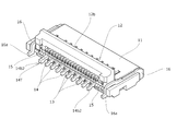
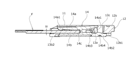
- FIG. 1 is an external perspective explanatory view showing the electrical connector shown in FIG. 1 from the rear side of the connector. It is front explanatory drawing when the electrical connector shown by FIG.1 and FIG.2 is seen from the connector front side.
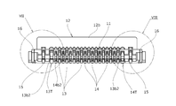
- FIG. 3 is an explanatory plan view when the electrical connector shown in FIGS. 1 and 2 is viewed from above the connector.
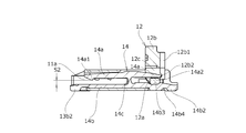
- FIG. 5 is a cross sectional explanatory view taken along line VV in FIG. 4.
- FIG. 6 is a cross sectional explanatory view taken along line VI-VI in FIG. 4.
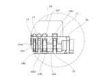
- FIG. 7 is a partial front enlarged explanatory view of a region indicated by VII in FIG. 3.
- FIG. 8 is a partial front enlarged explanatory view of a region indicated by VIII in FIG. 3.
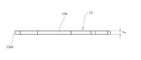
- FIG. 9 is an enlarged external perspective view illustrating the first conductive contact member used in the electrical connector according to the embodiment of the present invention shown in FIGS. 1 to 8 from the front side of the connector.
- FIG. 10 is an enlarged side view illustrating the first conductive contact member shown in FIG. 9 in a side view.
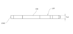
- FIG. 10 is an enlarged external perspective view illustrating the first thick conductive contact member in which the thickness of the first conductive contact member shown in FIG. 9 is increased from the front side of the connector.
- FIG. 12 is an enlarged plan view illustrating the first thick conductive contact member shown in FIG.
- FIG. 9 is an enlarged external perspective view illustrating the second conductive contact member used in the electrical connector according to the embodiment shown in FIGS. 1 to 8 from the front side of the connector.
- FIG. 14 is an enlarged plan view illustrating the second conductive contact member shown in FIG. 13 when viewed from above.
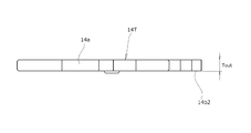
- FIG. 14 is an enlarged external perspective view illustrating the second thick conductive contact member having an increased thickness of the second conductive contact member shown in FIG. 13 from the front side of the connector.
- FIG. 16 is an enlarged side explanatory view showing a side view of the second thick conductive contact member shown in FIG. 15.
- FIG. 6 is a cross-sectional explanatory view corresponding to FIG. 5 in a clamped state after inserting a terminal portion of a flat signal transmission medium (FPC or FFC or the like) into the electrical connector according to the present invention.
- FIG. 7 is a cross-sectional explanatory view corresponding to FIG. 6 in a clamped state after inserting a terminal portion of a flat signal transmission medium (FPC or FFC or the like) into the electrical connector according to the present invention.
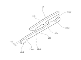
- the electrical connector 10 shown in FIGS. 1 to 8 is a so-called back flip type structure having an actuator 12 as connection operation means on the rear end edge side (the right end edge side in FIGS. 5 and 6) of the insulating housing 11.
- the actuator 12 described above is a rear side opposite to the front end side of the connector (the left end side in FIGS. 5 and 6) into which the terminal portion of the flat signal transmission medium (FPC or FFC) F is inserted. It is made the structure rotated so that it may be pushed down toward the (right side of FIG.5 and FIG.6).
- the insulating housing 11 at this time is formed of a hollow frame-like insulating member extending in an elongated shape.
- the longitudinal width direction of the insulating housing 11 is hereinafter referred to as a “connector longitudinal direction”, and is a flat plate.
- the direction in which the terminal portion of the signal transmission medium (FPC or FFC or the like) F is inserted and removed is referred to as “connector front” or “connector rear”.
- the height direction that is perpendicular to the surface of the printed wiring board on which the electrical connector 10 is mounted is defined as “upward”, and the opposite direction is defined as “downward”.
- the first and second conductive contact members 13 and 14 having two different shapes formed by a thin plate-like metal member are formed in a multipolar shape over a plurality of bodies. It is arranged to make.
- the first and second conductive contact members 13 and 14 are mounted in the insulating housing 11 at appropriate intervals along the “connector longitudinal direction” and have different shapes. 13 and the second conductive contact member 14 have a so-called staggered structure in which the multi-polar arrangement direction is alternately arranged in the “connector longitudinal direction”.
- Each of the first and second conductive contact members 13 and 14 is used for either signal transmission or ground connection, and is a wiring land portion (conductive path) formed on a printed wiring board (not shown). ) By solder bonding, whereby the electrical connector 10 is put into a mounted state.
- a signal transmission medium comprising a flexible printed circuit (FPC), a flexible flat cable (FFC), or the like.
- a medium insertion slot 11a into which a terminal portion of F is inserted is provided so as to be horizontally elongated in the connector longitudinal direction, and the rear end edge side of the connector front-rear direction on the opposite side (the right end in FIGS. 5 and 6)
- a component attachment port for mounting the above-described conductive contact member 13, actuator (connection operation means) 12, etc. is also formed in a horizontally elongated shape.
- the first conductive contact member 13 described above is mounted by being inserted from the medium insertion port 11a provided on the connector front end side of the insulating housing 11 toward the connector rear side (right side in FIG. 5).
- the second conductive contact member 14 is mounted by being inserted toward the front side of the connector (left side in FIG. 6) from the component attachment port provided on the connector rear end side of the insulating housing 11.
- Each of the first and second conductive contact members 13 and 14 has a transmission pattern Fa (see FIG. 17) formed on a flat signal transmission medium (FPC or FFC or the like) F inserted into the insulating housing 11.
- the transmission pattern Fa formed on the flat signal transmission medium F is arranged at a position corresponding to the signal transmission wiring land portion (signal line pad) or shield wiring land portion (shield line pad) as appropriate. It has the structure arrange
- Each of the first and second conductive contact members 13, 14 is along a “connector front-rear direction” that is a direction in which a flat signal transmission medium (FPC, FFC, etc.) F is inserted or removed (the left-right direction in FIGS. 5 and 6).
- the upper beams 13a and 14a and the lower beams 13b and 14b are formed of a pair of elongated beam members extending substantially in parallel.
- the upper beams 13a and 14a and the lower beams 13b and 14b are arranged so as to face each other at an appropriate interval in the “vertical direction” in the internal space of the insulating housing 11 described above.
- the lower beams 13b and 14b are arranged so as to be substantially immobile along the inner wall surface of the bottom plate of the insulating housing 11, and upward from an intermediate position in the extending direction of the lower beams 13b and 14b.
- the movable upper beams 13a and 14a are integrally connected to the above-described lower beams 13b and 14b via the extending connection support portions 13c and 14c.
- the connecting struts 13c and 14c are formed of narrow plate-like members, and are arranged so as to extend in the vertical direction at substantially the center portion in the extending direction of the beams 13a and 14a and 13b and 14b. ing. Then, the upper beams 13a and 14a rotate around the connection column portions 13c and 14c or the vicinity thereof by the elastic flexibility of the connection column portions 13c and 14c and the beams 13a and 14a and 13b and 14b. The lower beam 13b, 14b is also elastically displaced along with the elastic displacement so as to swing around the center. At this time, the upper beams 13a and 14a and the lower beams 13b and 14b are swung in the vertical direction within the plane of FIG. 5 and FIG.
- a transmission pattern (on the upper surface side of the flat signal transmission medium (FPC, FFC, etc.) F) is formed on the front end side portions (left end side portions in FIGS. 5 to 8) of the upper beams 13a and 14a described above.
- the upper terminal contact protrusions 13a1 and 14a1 connected to either one of the signal transmission or shield wiring land portions Fa are provided so as to form a downward protruding shape in the figure.
- the lower beams 13 b and 14 b are arranged so as to extend in the front-rear direction along the inner wall surface of the bottom plate of the insulating housing 11, but the flat signal transmission medium ( FPC or FFC) F is arranged such that the lower surface of the flat signal transmission medium F contacts the upper edges of the lower beams 13b and 14b described above. Further, the upper terminal contact protrusions 13a1 and 14a1 of the upper beams 13a and 14a are in contact with the upper surface of the flat signal transmission medium F so as to press from above. In this manner, the lower signal beams 13b and 14b and the upper beams 13a and 14a are in pressure contact with the upper and lower surfaces of the flat signal transmission medium F so as to be sandwiched from both sides. Clamping is performed (see FIGS. 18 to 20). The sandwiching operation of the flat signal transmission medium F will be described in detail later.
- the upper terminal contact protrusions 13a1 and 14a1 of the upper beams 13a and 14a are positioned relative to the lower beams 13b and 14b at the connector front side (left side in FIGS. 5 and 6) or the connector rear side (FIGS. 5 and 5). 6 (right side of 6) can also be arranged.
- the lower beams 13b and 14b are basically arranged so as to be substantially immobile, but for the purpose of temporarily holding the inserted flat signal transmission medium (FPC or FFC or the like) F,
- the portions can be formed so as to be elastically displaceable, and the front end portions of the lower beams 13b and 14b can be formed so as to slightly float from the inner wall surface of the bottom plate of the insulating housing 11.
- the rear end portion (the right end portion in FIGS. 5 and 6) of the lower beam 13b and the front end portion (the left end portion in FIGS. 5 and 6) of the lower beam 14b are disposed on the printed circuit board.
- These board connection parts 13b2 and 14b2 are placed in a state of being aligned from above with respect to the wiring land part (conductive path) on the printed wiring board, and are electrically connected by a collective joining operation using a solder material. Connection is made.
- solder relief portions 13b4 and 14b4 are formed. These solder relief portions 13b4 and 14b4 serve as portions for stopping the flow of the solder material that has been in a molten state during the soldering operation, and the concave space portions forming the solder relief portions 13b4 and 14b4.
- solder material fillet is formed at the corners near the board connecting portions 13b2 and 14b2, so that the flow of the solder material is stopped, and the solder relief portions 13b4 and 14b4 have other concave space portions.
- the solder material does not wrap around.
- cam pressure receiving portions 13a2 and 14a2 extending so as to form a substantially flat lower edge are provided on rear end portions (right end portions in FIGS. 5 and 6) of the upper beams 13a and 14a.
- cam slide receiving recesses 13b3 and 14b3 formed so as to form an upper edge of the concave shape are provided on the rear end side portions (the right end side portions in FIGS. 5 and 6) of the lower beams 13b and 14b, respectively.
- the lower half side portion of the pressing cam portion 12a of the actuator (connection operating means) 12 mounted on the rear end portion of the insulating housing 11 described above. Is arranged so as to be slidable from above, and by such a slidable contact arrangement relationship, the actuator 12 is rotatably supported around the rotation center of the pressing cam portion 12a. ing.
- a cam surface is formed on the outer periphery of the above-described pressing cam portion 12a, and the cam pressure receiving portions 13a2 of the upper beams 13a and 14a are opposed to the cam surface formed on the upper half side portion of the pressing cam portion 12a.
- 14a2 is arrange
- the electrical connector 10 has a structure in which the length in the connector longitudinal direction, which is a multipolar arrangement direction, is reduced as much as possible based on the recent demand for miniaturization in electronic devices. . More specifically, the thickness of the first and second conductive contact members 13 and 14 in the multipolar arrangement direction is reduced, thereby arranging the first and second conductive contact members 13 and 14. The pitch is narrowed and the total length in the connector longitudinal direction is shortened. On the other hand, when the first and second conductive contact members 13 and 14 are thinned, their conductor resistance increases, the allowable current value of the transmission signal decreases, and the allowable power supply to the electrical connector 10 tends to decrease. Will occur.
- the thickness of at least one of the first and second conductive contact members 13 and 14 arranged over a plurality of bodies is set. It is formed to be thicker than other contact members. More specifically, among the plurality of first and second conductive contact members 13 and 14 arranged in a multipolar manner, the outermost ends on both sides in the multipolar arrangement direction (connector longitudinal direction). The thicknesses of the first and second conductive contact members 13T and 14T arranged at the positions are increased. Then, the other thin conductive contact members 13 and 14 are sandwiched between the first and second thick conductive contact members 13T and 14T arranged at the outermost ends on both sides. It is made the arrangement arranged.
- Tout is approximately the thickness Tin (see FIGS. 9, 10 and 13, 14) of the other first and second thin conductive contact members 13 and 14. It is set to 2 times (Tout ⁇ 2 Tin).
- the thickness Tout of the first thick conductive contact member 13T and the thickness Tout of the second thick conductive contact member 14T are set to the same thickness dimension. However, it is also possible to set different thickness dimensions.
- first thick conductive contact member 13T having the increased thickness and the other first thin conductive contact member 13 are the same when viewed in the multipolar arrangement direction.
- second thick conductive contact member 14T and the other second thin conductive contact member 14 are identical when viewed in the multipolar arrangement direction. It has a shape. With this configuration, the conductive contact members 13 and 14 are all assembled in the same manner regardless of the thickness.
- the first and second conductive contact members 13 and 14 in the present embodiment are formed from one of the two types of shapes described above regardless of the thickness, so that the thickness is increased. Even in the case where the increased first and second thick conductive contact members 13T and 14T are mixed with the other first and second thin conductive contact members 13 and 14, It is possible to have the same arrangement relationship as the one, and as in this embodiment, a so-called staggered arrangement in which different shapes are alternately arranged in the multipolar arrangement direction (connector longitudinal direction) It is possible to adopt.
- the conductors of the first and second thick conductive contact members 13T and 14T which are increased in thickness and are arranged at the outer ends on both sides. Since the resistance is reduced according to the increase in thickness, the energization allowable power in the transmission signal is increased, and even if the power supplied to the electrical connector 10 is large, the conductive contact members 13 and 14 as a whole. There is no need to increase the number of. Therefore, an increase in size such as an increase in the length or height of the electrical connector 10 is suppressed.
- the contact portions of the first and second thick conductive contact members 13T and 14T with respect to the surface of the flat signal transmission medium (FPC or FFC or the like) F inserted inside the insulating housing 11 are: That is, the upper terminal contact protrusions 13a1, 14a1 and the upper edges of the lower beams 13b, 14b having increased thickness are in pressure contact with each other, so that the conductive contact member 13, 14 increases, so that the retention property of the flat signal transmission medium F is enhanced.
- the first and second thick conductive contact members 13T and 14T arranged at the outermost ends on both sides of the multipolar arrangement direction (connector longitudinal direction) are provided. Since the other two thin-walled conductive contact members 13 and 14 are arranged so as to sandwich the multipolar arrangement direction, the first and second thick-walled conductive members having a relatively large contact pressure.
- the contact portions of the contact members 13T and 14T are located on both sides of the other thin conductive contact members 13 and 14 (outermost end positions) with respect to the flat signal transmission medium (FPC or FFC) F To be in a pressure contact state.
- FPC or FFC flat signal transmission medium
- FIG. 6 As shown in FIG. 6, intervals S ⁇ b> 1 and S ⁇ b> 2 are formed in which a flat signal transmission medium (FPC or FFC or the like) F can be inserted.
- FPC flat signal transmission medium
- the distances S1 and S2 formed in the first and second thick conductive contact members 13T and 14T having increased thicknesses correspond to the connector insertion portion of the flat signal transmission medium F. It is set equal to or smaller than the thickness Tf (see FIGS. 19 and 20) (S1, S2 ⁇ Tf).
- the first and second thicknesses of the flat signal transmission medium (FPC or FFC) F immediately after being inserted into the insulating housing 11 are increased.
- the contact portions of the thick conductive contact members 13T and 14T are immediately brought into contact with each other, and the contact portions of the first and second thick conductive contact members 13T and 14T have a relatively large contact.
- the flat signal transmission medium F is temporarily held by the pressure. Accordingly, the flat signal transmission medium F is stably held during the period from the insertion of the flat signal transmission medium F to the completion of clamping.
- the entirety of the actuator (connection operation means) 12 arranged so as to be rotated to the rear end portion (the right end side portion in FIGS. 5 and 6) of the insulating housing 11 extends along the connector longitudinal direction.
- the insulating housing 11 is arranged so as to extend in a slender shape over almost the same length as the entire width of the insulating housing 11.
- the actuator 12 is attached so as to be rotatable around the rotation center extending in the longitudinal direction of the actuator 12, that is, the rotation center of the pressing cam portion 12a described above.
- An outer side portion (upper side portion in FIGS. 5 and 6) is formed in the opening / closing operation portion 12b.
- the entire actuator 12 is in the “initial standby position” in a substantially upright state as shown in FIGS. 1 to 8 and FIG. ”And the“ operation clamping position ”in a state of being tilted almost horizontally toward the rear side of the connector as shown in FIGS. 18 to 20.
- the upper beam of the first and second conductive contact members 13 and 14 is provided on the rotation center side portion connected to the above-described pressing cam portion 12a.
- a plurality of slit holes 12c for avoiding interference with 13a, 14a are formed in a comb-teeth shape parallel to each other at a constant interval along the “connector longitudinal direction”.
- the slit holes 12c are formed so as to penetrate through the opening / closing operation portion 12b of the actuator 12 in the “connector longitudinal direction” at positions corresponding to the conductive contact members 13 and.
- the actuator (connection operation means) 12 is rotated from the “operation holding position” (see FIGS. 18 to 20) toward the “initial standby position” (see FIGS. 1 to 8 and 17).
- the actuator 12 is arranged so as to rise from the wiring board, the upper beams 13a and 14a constituting the first and second conductive contact members 13 and 14 are directed inward of the slit hole 12c described above.
- the rear end portion is inserted.
- the insertion at this time is performed from the front of the operation unit, which is the front side of the opening / closing operation unit 12b of the actuator 12, and the rear end portions of the upper beams 13a and 14a penetrating the slit hole 12c are connected to the opening / closing operation unit 12b of the actuator 12. It is made in a state of projecting outward (rearward) from the operation unit rear surface 12b1 which is the rear surface side.
- the opening / closing operation part 12b of the actuator (connection operation means) 12 is moved from the “initial standby position” (see FIGS. 1 to 8 and 17) to the “operation clamping position” (see FIGS. 18 to 20).
- the rotation radius of the pressing cam portion 12a described above changes in a direction increasing between the lower beams 13b and 14b and the upper beams 13a and 14a. ing.
- the cam pressure receiving portions 13a2 and 14a2 provided on the rear ends of the upper beams 13a and 14a are displaced so as to be lifted upward in the drawing, and accordingly.
- Upper terminal contact convex portions 13a1 and 14a1 provided on the opposite side (connector front end side) to the cam pressure receiving portions 13a2 and 14a2 are pushed downward.
- the lock members 15, which are formed of elongated plate-like metal members, 15 is attached to the insulating housing 11.
- These locking members 15 and 15 are arranged so as to extend substantially in parallel to the first and second conductive contact members 13 and 14 described above, and a flat signal transmission medium (such as FPC or FFC).
- Locking protrusions (not shown) that can be engaged with positioning recesses Fb and Fb (see FIG. 19) formed on both side edges of F are provided.
- the actuator (connection operation means) 12 is rotated to the “operation holding position” (see FIGS. 10 to 18)
- the lock members 15 and 15 described above are positioned in the positioning recesses Fb and Fb of the signal transmission medium F.
- the signal transmission medium F is held so that it does not come out of the final insertion position.
- fixing brackets 16, 16 made of an elongated plate-like metal member are attached to the insulating housing 11 at the outer portions on both sides in the “connector longitudinal direction” with respect to the lock members 15, 15 described above. These fixing brackets 16 and 16 are arranged so as to extend substantially parallel to the conductive contact members 13 and 14 and the lock member 15 described above, and printed wiring boards are provided at both ends in the extending direction. Solder fixing portions 16a, 16a are provided which are placed on a fixing pad (not shown) formed on P and soldered.
- the operation unit rear surface of the opening / closing operation unit 12b of the actuator 12 is In this case, the operation unit rear surface of the actuator 12 constitutes the second conductive contact member 14 and is arranged so as to form a lower surface extending substantially parallel to the mounting surface of the printed wiring board.
- the lower beam 14b extends in the extending direction above the rear end portion, that is, above the substrate connecting portion 14b2.
- the opening / closing operation portion 12b of the actuator (connection operation means) 12 is provided with the protective projection portion 12b2 (see FIGS. 5 and 6) protruding from the back surface of the operation portion. That is, the protective protrusion 12b2 is formed so as to protrude from the rear surface of the operation unit of the actuator 12 toward the rear side of the connector when the actuator 12 is in the “initial standby position”. It is arranged in a portion between a pair of first and second conductive contact members 13 and 14 adjacent to each other in the connector longitudinal direction.
- the protective projection 12b2 provided on the rear surface of the operation unit of the actuator (connection operation means) 12 has an “initial standby position” (so that the actuator 12 rises from the printed wiring board). 1 to 8 and 17), the first conductive contact member 13 is arranged between the upper beam 13a and the second conductive contact member 14 and the upper beam 14a.
- the protective projections 12b2 are arranged adjacent to the rear end portions of the pair of upper beams 13a, 14a in the multipolar arrangement direction (connector longitudinal direction), so that The upper beam 13a, the protective projection 12b2, and the upper beam 14a are arranged in parallel in the multipolar arrangement direction (connector longitudinal direction).
- the protrusion height of the protective projection 12b2 in the state where the actuator (connection operation means) 12 is arranged at the “initial standby position” (see FIGS. 1 to 8 and 17), that is, the operation unit rear surface of the actuator 12 is
- the protruding height when the reference surface is used is set so that the rear end portions of the upper beams 13a and 14a are the same or slightly larger than the height protruding from the operation unit back surface as the reference surface. . That is, the rear end portions of the upper beams 13a and 14a of the conductive contact members 13 and 14 when the actuator 12 is arranged at the “initial standby position” so as to rise from the printed wiring board are outside the operation unit rear surface 12b1 of the actuator 12.
- the upper end of the upper beams 13a and 14a protrudes in the same direction as the protruding end of the protective projection 12b2 provided on the actuator 12 side, or is retracted. Will be placed at the position. As a result, the fingertips and nails of the rotating operator may come into contact with the protective projection 12b2 of the actuator 12, but the rear ends of the upper beams 13a and 14a of the first and second conductive contact members 13 and 14 This prevents the parts from being caught and prevents the conductive contact members 13 and 14 from being deformed or damaged during the turning operation.
- the protective protrusion provided on the back of the operation portion of the opening / closing operation portion 12b of the actuator (connection operation means) 12 The portion 12b2 protrudes toward the lower side, which is the printed wiring board side.
- the protective projection 12b2 is positioned above the solder relief portion 13b4 provided on the first conductive contact member 13. It is made in the arrangement relation. That is, when soldering the conductive contact members 13 and 14, since the solder material does not rotate in the solder release portions 13b4 and 14b4, the solder release portion provided in the first conductive contact member 13 as described above.
- the protective protrusion 12b2 may come into contact with the solder material even when the actuator 12 is rotated to the “operation clamping position”. As a result, the reliability of solder bonding is ensured.
- the thickness of the two conductive contact members disposed at the outermost positions on both sides in the multipolar arrangement direction is increased.
- any one of all the conductive contact members may be formed in a thick shape with an increased thickness.
- the thickness of the pair of conductive contact members having different shapes is increased.
- a configuration in which the thickness of a plurality of (three or more) conductive contact members is increased can also be adopted.
- a configuration in which the thickness of a pair or a plurality of conductive contact members having the same shape is increased can be employed.
- the electrical connector according to the above-described embodiment uses a conductive contact member having a different shape
- the present invention is similarly applied to an electrical connector using a conductive contact member having the same shape. Is possible.
- a flexible printed circuit (FPC) and a flexible flat cable (FFC) are employed as the flat signal transmission medium to be inserted into the electrical connector in the above-described embodiment.
- the present invention can be similarly applied to the case where a medium or the like is used.
- connection operation means in the above-described embodiment is configured by an actuator that is rotated.
- the present invention can be similarly applied to an electrical connector having a connection operation means that is slid. It is.
- the present invention relates to an electrical connector in which the connection operation means (actuator) is disposed at the front end side portion, or an electrical connector in which the connection operation means (actuator) is disposed between the front end side portion and the rear end side portion.
- the rotation direction or the sliding direction of the connection operation means (actuator) at that time may be either the front side or the rear side.
- the present invention can be widely applied to a wide variety of electrical connectors used for various electrical devices.
Landscapes
- Coupling Device And Connection With Printed Circuit (AREA)
Abstract
Description
11 絶縁ハウジング
11a 媒体挿入口
12 アクチュエータ(接続操作手段)
12a 押圧カム部
12b 開閉操作部
12b2 保護突起部
12c スリット穴
13,14 第1及び第2の導電コンタクト部材
13T,14T 第1及び第2の厚肉状導電コンタクト部材
13a,14a 可動上ビーム
13a1,14a1 上端子接触凸部
13a2,14a2 カム圧受け部
13b3,14b3 カム滑り受凹部
13b,14b 固定下ビーム
13b4,14b4 半田逃がし部
13c,14c 連結支柱部
15 ロック部材
16 固定金具
16a 半田固定部
F 平板状信号伝送媒体(FPC又はFFC等)
Fa 伝送パターン
Fb 位置決め凹部
Claims (6)
- 絶縁ハウジングに取り付けられた複数体のコンタクト部材が、当該コンタクト部材の厚さ方向に沿って多極状に配列されたものであって、
前記絶縁ハウジングの内部に挿入された平板状信号伝送媒体の両側表面に、前記コンタクト部材に設けられた一対の接触部が両側から挟むように圧接することで前記平板状信号伝送媒体の挟持が行われる構成になされた電気コネクタにおいて、
前記複数体のコンタクト部材の少なくとも一体の厚さが、他のコンタクト部材より厚く形成されていることを特徴とする電気コネクタ。 - 前記他のコンタクト部材より厚く形成されたコンタクト部材が、前記多極状の配列方向において前記他のコンタクト部材を挟むように2体配置されていることを特徴とする請求項1記載の電気コネクタ。
- 前記2体のコンタクト部材が、前記多極状の配列方向における両側の最外端の位置に配置されていることを特徴とする請求項2記載の電気コネクタ。
- 前記他のコンタクト部材より厚く形成されたコンタクト部材に設けられた一対の接触部同士の間隔Sが、前記平板状信号伝送媒体の厚さTと同一又は小さく設定されている(S≦T)ことを特徴とする請求項1記載の電気コネクタ。
- 前記他のコンタクト部材と、当該他のコンタクト部材より厚く形成されたコンタクト部材とが、前記多極状の配列方向に見たときに同一の形状を備えていることを特徴とする請求項1記載の電気コネクタ。
- 前記他のコンタクト部材と、当該他のコンタクト部材より厚く形成されたコンタクト部材とを含む複数のコンタクト部材の各々が、前記多極状の配列方向に見たときに互いに異なる形状を有する2種類のコンタクト部材のいずれかから形成されていることを特徴とする請求項1記載の電気コネクタ。
Priority Applications (4)
| Application Number | Priority Date | Filing Date | Title |
|---|---|---|---|
| EP16821143.1A EP3327872A4 (en) | 2015-07-08 | 2016-06-03 | ELECTRICAL CONNECTOR |
| CN201680051711.9A CN108028482B (zh) | 2015-07-08 | 2016-06-03 | 电连接器 |
| US15/757,370 US10418733B2 (en) | 2015-07-08 | 2016-06-03 | Electric connector with contact members having different thickness |
| KR1020187003950A KR102147588B1 (ko) | 2015-07-08 | 2016-06-03 | 전기 커넥터 |
Applications Claiming Priority (2)
| Application Number | Priority Date | Filing Date | Title |
|---|---|---|---|
| JP2015-136599 | 2015-07-08 | ||
| JP2015136599A JP6592995B2 (ja) | 2015-07-08 | 2015-07-08 | 電気コネクタ |
Publications (1)
| Publication Number | Publication Date |
|---|---|
| WO2017006672A1 true WO2017006672A1 (ja) | 2017-01-12 |
Family
ID=57685714
Family Applications (1)
| Application Number | Title | Priority Date | Filing Date |
|---|---|---|---|
| PCT/JP2016/066589 Ceased WO2017006672A1 (ja) | 2015-07-08 | 2016-06-03 | 電気コネクタ |
Country Status (7)
| Country | Link |
|---|---|
| US (1) | US10418733B2 (ja) |
| EP (1) | EP3327872A4 (ja) |
| JP (1) | JP6592995B2 (ja) |
| KR (1) | KR102147588B1 (ja) |
| CN (1) | CN108028482B (ja) |
| TW (2) | TWI687001B (ja) |
| WO (1) | WO2017006672A1 (ja) |
Families Citing this family (10)
| Publication number | Priority date | Publication date | Assignee | Title |
|---|---|---|---|---|
| JP6996521B2 (ja) * | 2019-02-20 | 2022-01-17 | I-Pex株式会社 | 電気コネクタ |
| JP6947195B2 (ja) | 2019-02-20 | 2021-10-13 | I−Pex株式会社 | 電気コネクタ |
| JP6841290B2 (ja) | 2019-02-20 | 2021-03-10 | I−Pex株式会社 | 電気コネクタ |
| USD941244S1 (en) * | 2019-06-25 | 2022-01-18 | Kyocera Corporation | Electric connector |
| CN112217045B (zh) * | 2019-07-11 | 2024-04-30 | 泰连公司 | 用于电路卡组件的电力连接器系统 |
| CN114467229A (zh) * | 2020-01-27 | 2022-05-10 | 日立安斯泰莫株式会社 | 电子控制装置 |
| JP2021118268A (ja) * | 2020-01-27 | 2021-08-10 | 日立Astemo株式会社 | 電子制御装置及びコネクタ |
| CN114665306B (zh) * | 2022-03-25 | 2024-02-20 | 鹤山市得润电子科技有限公司 | 一种连接器及电子设备 |
| JP1746290S (ja) * | 2023-01-31 | 2023-06-14 | 電気コネクタ | |
| JP1746547S (ja) * | 2023-01-31 | 2023-06-16 | 電気コネクタ |
Citations (5)
| Publication number | Priority date | Publication date | Assignee | Title |
|---|---|---|---|---|
| JPH11204204A (ja) * | 1998-01-07 | 1999-07-30 | Jst Mfg Co Ltd | コネクタ |
| JPH11307198A (ja) * | 1998-04-17 | 1999-11-05 | Smk Corp | プリント配線板用コネクター |
| JP2006040687A (ja) * | 2004-07-27 | 2006-02-09 | Taiko Denki Co Ltd | 基板間コネクタ |
| JP4908621B1 (ja) * | 2010-10-15 | 2012-04-04 | 株式会社東芝 | 電子機器 |
| JP2012069481A (ja) * | 2010-09-27 | 2012-04-05 | Kyocera Elco Corp | コネクタ |
Family Cites Families (10)
| Publication number | Priority date | Publication date | Assignee | Title |
|---|---|---|---|---|
| JPS498621A (ja) | 1972-05-29 | 1974-01-25 | ||
| US4196955A (en) * | 1979-02-07 | 1980-04-08 | International Telephone And Telegraph Corporation | Zero insertion force connector |
| US5830014A (en) * | 1992-11-25 | 1998-11-03 | Berg Technology, Inc. | Electrical connector |
| CN2351881Y (zh) * | 1998-12-29 | 1999-12-01 | 富士康(昆山)电脑接插件有限公司 | 电连接器嵌扣装置 |
| JP2010056066A (ja) * | 2008-07-29 | 2010-03-11 | Yamaichi Electronics Co Ltd | ケーブル用コネクタ |
| JP2012151021A (ja) * | 2011-01-20 | 2012-08-09 | D D K Ltd | コネクタ |
| JP6021058B2 (ja) * | 2012-08-27 | 2016-11-02 | パナソニックIpマネジメント株式会社 | コネクタ |
| TWM476383U (en) * | 2013-05-31 | 2014-04-11 | Advanced Connectek Inc | Connector |
| JP5574514B2 (ja) * | 2013-06-18 | 2014-08-20 | ヒロセ電機株式会社 | 回路基板用電気コネクタ |
| JP6215042B2 (ja) * | 2013-12-24 | 2017-10-18 | 日本航空電子工業株式会社 | 電気コネクタ |
-
2015
- 2015-07-08 JP JP2015136599A patent/JP6592995B2/ja active Active
-
2016
- 2016-06-03 KR KR1020187003950A patent/KR102147588B1/ko not_active Expired - Fee Related
- 2016-06-03 US US15/757,370 patent/US10418733B2/en active Active
- 2016-06-03 EP EP16821143.1A patent/EP3327872A4/en not_active Withdrawn
- 2016-06-03 WO PCT/JP2016/066589 patent/WO2017006672A1/ja not_active Ceased
- 2016-06-03 CN CN201680051711.9A patent/CN108028482B/zh not_active Expired - Fee Related
- 2016-06-08 TW TW105118125A patent/TWI687001B/zh not_active IP Right Cessation
- 2016-06-08 TW TW107109862A patent/TWI687002B/zh not_active IP Right Cessation
Patent Citations (5)
| Publication number | Priority date | Publication date | Assignee | Title |
|---|---|---|---|---|
| JPH11204204A (ja) * | 1998-01-07 | 1999-07-30 | Jst Mfg Co Ltd | コネクタ |
| JPH11307198A (ja) * | 1998-04-17 | 1999-11-05 | Smk Corp | プリント配線板用コネクター |
| JP2006040687A (ja) * | 2004-07-27 | 2006-02-09 | Taiko Denki Co Ltd | 基板間コネクタ |
| JP2012069481A (ja) * | 2010-09-27 | 2012-04-05 | Kyocera Elco Corp | コネクタ |
| JP4908621B1 (ja) * | 2010-10-15 | 2012-04-04 | 株式会社東芝 | 電子機器 |
Non-Patent Citations (1)
| Title |
|---|
| See also references of EP3327872A4 * |
Also Published As
| Publication number | Publication date |
|---|---|
| TWI687002B (zh) | 2020-03-01 |
| US20180254572A1 (en) | 2018-09-06 |
| TW201826629A (zh) | 2018-07-16 |
| KR20180035225A (ko) | 2018-04-05 |
| JP2017021911A (ja) | 2017-01-26 |
| KR102147588B1 (ko) | 2020-08-24 |
| EP3327872A4 (en) | 2019-04-10 |
| TWI687001B (zh) | 2020-03-01 |
| US10418733B2 (en) | 2019-09-17 |
| CN108028482B (zh) | 2019-12-13 |
| JP6592995B2 (ja) | 2019-10-23 |
| EP3327872A1 (en) | 2018-05-30 |
| CN108028482A (zh) | 2018-05-11 |
| TW201711293A (zh) | 2017-03-16 |
Similar Documents
| Publication | Publication Date | Title |
|---|---|---|
| JP6592995B2 (ja) | 電気コネクタ | |
| TWI455408B (zh) | 用於電子連接器之接腳組織器 | |
| JP4098290B2 (ja) | Ffc用コネクタ | |
| CN102983450B (zh) | 电连接器 | |
| JP6308197B2 (ja) | 電気コネクタ | |
| CN101390257A (zh) | 用于扁平电缆的电连接器 | |
| JP2016129124A (ja) | 電気コネクタ | |
| US9252516B2 (en) | Connector | |
| WO2011016538A1 (ja) | フレキシブル集約配線コネクタ | |
| US9240642B2 (en) | Connector | |
| DK2710679T3 (en) | DEVICE INCLUDING A CONNECTOR AND A PRINTING PLATE | |
| US7165991B2 (en) | Connector | |
| JP6569851B2 (ja) | 電気コネクタ | |
| JP2017103143A (ja) | 電気コネクタ | |
| JP5428369B2 (ja) | 電気回路基板の製造方法 | |
| KR101311482B1 (ko) | 컨택트의 구조가 개선된 플랫 케이블 커넥터 | |
| JP5218441B2 (ja) | 電気コネクタ | |
| JP6513524B2 (ja) | コネクタ | |
| JP2013134870A (ja) | 電気コネクタ | |
| JP2024037253A (ja) | コネクタ及び電子基板 | |
| JPH0773915A (ja) | プリント基板の接続装置 | |
| KR20240031710A (ko) | 오조립 방지 구조를 가지는 배터리셀 연결장치 | |
| WO2022049945A1 (ja) | フレキシブルプリント基板の接続構造およびフレキシブルプリント基板ユニットの製造方法 | |
| JP2018045801A (ja) | 電気コネクタ | |
| JP2019003755A (ja) | 電気コネクタ |
Legal Events
| Date | Code | Title | Description |
|---|---|---|---|
| 121 | Ep: the epo has been informed by wipo that ep was designated in this application |
Ref document number: 16821143 Country of ref document: EP Kind code of ref document: A1 |
|
| NENP | Non-entry into the national phase |
Ref country code: DE |
|
| ENP | Entry into the national phase |
Ref document number: 20187003950 Country of ref document: KR Kind code of ref document: A |
|
| WWE | Wipo information: entry into national phase |
Ref document number: 2016821143 Country of ref document: EP |
|
| WWE | Wipo information: entry into national phase |
Ref document number: 15757370 Country of ref document: US |