WO2017010004A1 - Dispositif de commande de mémoire, dispositif de traitement d'informations et dispositif de traitement - Google Patents
Dispositif de commande de mémoire, dispositif de traitement d'informations et dispositif de traitement Download PDFInfo
- Publication number
- WO2017010004A1 WO2017010004A1 PCT/JP2015/070438 JP2015070438W WO2017010004A1 WO 2017010004 A1 WO2017010004 A1 WO 2017010004A1 JP 2015070438 W JP2015070438 W JP 2015070438W WO 2017010004 A1 WO2017010004 A1 WO 2017010004A1
- Authority
- WO
- WIPO (PCT)
- Prior art keywords
- data
- memory
- cache
- controller
- nonvolatile
- Prior art date
- Legal status (The legal status is an assumption and is not a legal conclusion. Google has not performed a legal analysis and makes no representation as to the accuracy of the status listed.)
- Ceased
Links
Images


Classifications
-
- G—PHYSICS
- G06—COMPUTING OR CALCULATING; COUNTING
- G06F—ELECTRIC DIGITAL DATA PROCESSING
- G06F12/00—Accessing, addressing or allocating within memory systems or architectures
- G06F12/02—Addressing or allocation; Relocation
- G06F12/08—Addressing or allocation; Relocation in hierarchically structured memory systems, e.g. virtual memory systems
- G06F12/0802—Addressing of a memory level in which the access to the desired data or data block requires associative addressing means, e.g. caches
- G06F12/0806—Multiuser, multiprocessor or multiprocessing cache systems
- G06F12/0808—Multiuser, multiprocessor or multiprocessing cache systems with cache invalidating means
-
- G—PHYSICS
- G06—COMPUTING OR CALCULATING; COUNTING
- G06F—ELECTRIC DIGITAL DATA PROCESSING
- G06F12/00—Accessing, addressing or allocating within memory systems or architectures
- G06F12/02—Addressing or allocation; Relocation
- G06F12/08—Addressing or allocation; Relocation in hierarchically structured memory systems, e.g. virtual memory systems
- G06F12/0802—Addressing of a memory level in which the access to the desired data or data block requires associative addressing means, e.g. caches
- G06F12/0806—Multiuser, multiprocessor or multiprocessing cache systems
- G06F12/0815—Cache consistency protocols
- G06F12/0831—Cache consistency protocols using a bus scheme, e.g. with bus monitoring or watching means
-
- G—PHYSICS
- G06—COMPUTING OR CALCULATING; COUNTING
- G06F—ELECTRIC DIGITAL DATA PROCESSING
- G06F3/00—Input arrangements for transferring data to be processed into a form capable of being handled by the computer; Output arrangements for transferring data from processing unit to output unit, e.g. interface arrangements
- G06F3/06—Digital input from, or digital output to, record carriers, e.g. RAID, emulated record carriers or networked record carriers
- G06F3/0601—Interfaces specially adapted for storage systems
- G06F3/0602—Interfaces specially adapted for storage systems specifically adapted to achieve a particular effect
- G06F3/061—Improving I/O performance
-
- G—PHYSICS
- G06—COMPUTING OR CALCULATING; COUNTING
- G06F—ELECTRIC DIGITAL DATA PROCESSING
- G06F3/00—Input arrangements for transferring data to be processed into a form capable of being handled by the computer; Output arrangements for transferring data from processing unit to output unit, e.g. interface arrangements
- G06F3/06—Digital input from, or digital output to, record carriers, e.g. RAID, emulated record carriers or networked record carriers
- G06F3/0601—Interfaces specially adapted for storage systems
- G06F3/0602—Interfaces specially adapted for storage systems specifically adapted to achieve a particular effect
- G06F3/0614—Improving the reliability of storage systems
-
- G—PHYSICS
- G06—COMPUTING OR CALCULATING; COUNTING
- G06F—ELECTRIC DIGITAL DATA PROCESSING
- G06F3/00—Input arrangements for transferring data to be processed into a form capable of being handled by the computer; Output arrangements for transferring data from processing unit to output unit, e.g. interface arrangements
- G06F3/06—Digital input from, or digital output to, record carriers, e.g. RAID, emulated record carriers or networked record carriers
- G06F3/0601—Interfaces specially adapted for storage systems
- G06F3/0628—Interfaces specially adapted for storage systems making use of a particular technique
- G06F3/0646—Horizontal data movement in storage systems, i.e. moving data in between storage devices or systems
- G06F3/065—Replication mechanisms
-
- G—PHYSICS
- G06—COMPUTING OR CALCULATING; COUNTING
- G06F—ELECTRIC DIGITAL DATA PROCESSING
- G06F3/00—Input arrangements for transferring data to be processed into a form capable of being handled by the computer; Output arrangements for transferring data from processing unit to output unit, e.g. interface arrangements
- G06F3/06—Digital input from, or digital output to, record carriers, e.g. RAID, emulated record carriers or networked record carriers
- G06F3/0601—Interfaces specially adapted for storage systems
- G06F3/0668—Interfaces specially adapted for storage systems adopting a particular infrastructure
- G06F3/0671—In-line storage system
- G06F3/0683—Plurality of storage devices
- G06F3/0688—Non-volatile semiconductor memory arrays
-
- G—PHYSICS
- G06—COMPUTING OR CALCULATING; COUNTING
- G06F—ELECTRIC DIGITAL DATA PROCESSING
- G06F12/00—Accessing, addressing or allocating within memory systems or architectures
- G06F12/02—Addressing or allocation; Relocation
- G06F12/08—Addressing or allocation; Relocation in hierarchically structured memory systems, e.g. virtual memory systems
- G06F12/0802—Addressing of a memory level in which the access to the desired data or data block requires associative addressing means, e.g. caches
- G06F12/0866—Addressing of a memory level in which the access to the desired data or data block requires associative addressing means, e.g. caches for peripheral storage systems, e.g. disk cache
- G06F12/0868—Data transfer between cache memory and other subsystems, e.g. storage devices or host systems
-
- G—PHYSICS
- G06—COMPUTING OR CALCULATING; COUNTING
- G06F—ELECTRIC DIGITAL DATA PROCESSING
- G06F2212/00—Indexing scheme relating to accessing, addressing or allocation within memory systems or architectures
- G06F2212/10—Providing a specific technical effect
- G06F2212/1016—Performance improvement
-
- G—PHYSICS
- G06—COMPUTING OR CALCULATING; COUNTING
- G06F—ELECTRIC DIGITAL DATA PROCESSING
- G06F2212/00—Indexing scheme relating to accessing, addressing or allocation within memory systems or architectures
- G06F2212/10—Providing a specific technical effect
- G06F2212/1032—Reliability improvement, data loss prevention, degraded operation etc
-
- G—PHYSICS
- G06—COMPUTING OR CALCULATING; COUNTING
- G06F—ELECTRIC DIGITAL DATA PROCESSING
- G06F2212/00—Indexing scheme relating to accessing, addressing or allocation within memory systems or architectures
- G06F2212/22—Employing cache memory using specific memory technology
- G06F2212/222—Non-volatile memory
-
- G—PHYSICS
- G06—COMPUTING OR CALCULATING; COUNTING
- G06F—ELECTRIC DIGITAL DATA PROCESSING
- G06F2212/00—Indexing scheme relating to accessing, addressing or allocation within memory systems or architectures
- G06F2212/31—Providing disk cache in a specific location of a storage system
- G06F2212/312—In storage controller
-
- G—PHYSICS
- G06—COMPUTING OR CALCULATING; COUNTING
- G06F—ELECTRIC DIGITAL DATA PROCESSING
- G06F2212/00—Indexing scheme relating to accessing, addressing or allocation within memory systems or architectures
- G06F2212/60—Details of cache memory
- G06F2212/604—Details relating to cache allocation
-
- G—PHYSICS
- G06—COMPUTING OR CALCULATING; COUNTING
- G06F—ELECTRIC DIGITAL DATA PROCESSING
- G06F2212/00—Indexing scheme relating to accessing, addressing or allocation within memory systems or architectures
- G06F2212/62—Details of cache specific to multiprocessor cache arrangements
- G06F2212/621—Coherency control relating to peripheral accessing, e.g. from DMA or I/O device
Definitions
- Embodiments described herein relate generally to a memory controller, an information processing apparatus, and a processing apparatus.
- main memory such as MRAM (Magnetoresistive Random Access Memory), PCM (Phase Change Memory), Memristor, etc.
- MRAM Magneticoresistive Random Access Memory
- PCM Phase Change Memory
- Memristor etc.
- the transaction processing system is also required to have high reliability, the data that guarantees the atomicity of writing to the nonvolatile memory (property that does not end in the middle of writing) and ordering (ordering) by the program executed on the processor.
- a permanent update processing method is required.
- the memory controller includes a nonvolatile cache memory and a controller.
- the nonvolatile cache memory is used for storing a part of data stored in a nonvolatile main memory connected to a memory controller.
- the controller controls writing to and reading from the nonvolatile cache memory.
- the memory controller is connected to the processing device via an interconnect that guarantees a protocol indicating a procedure for maintaining and managing cache coherency so that data mismatch between a plurality of cache memories does not occur. You may connect with a bus
- the controller uses the protocol to detect that the processing device has updated the data stored in any area of the nonvolatile main memory, and then sends the updated data to the memory controller. Are written in the non-volatile cache memory.
- FIG. 1 is a diagram illustrating an example of a configuration of an information processing apparatus according to a first embodiment.
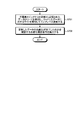
- FIG. 6 is a diagram illustrating an operation example of the memory controller according to the first embodiment.
- FIG. 3 is a diagram illustrating an operation example of the information processing apparatus according to the first embodiment.
- a nonvolatile cache memory that operates at a higher speed than the high-speed nonvolatile memory for these main memories is built in a memory controller connected to the nonvolatile main memory, and the data written in the nonvolatile cache memory is permanently stored.
- the commit process is further accelerated by guaranteeing the performance.
- the non-volatile cache memory is, for example, a non-volatile memory such as MRAM, PCM, and Memristor that operates at the same speed as an SRAM.
- the memory controller 100 incorporating the nonvolatile cache memory 10 includes a plurality of MESIF protocols, a protocol implemented by the QPI described later (QPI protocol), a MESI protocol, a MOESI protocol, and the like.
- QPI Intelligent QuickPath Interconnect
- a high-speed interconnect (cache coherent interconnect) 200 is connected to a processor (typically a CPU, which corresponds to a “processing device”) 300.
- processor typically a CPU, which corresponds to a “processing device”
- These cache coherence protocols are generally designed for connecting processors, but in the present embodiment, a memory controller is connected to the processors and used for control from the memory controller side.
- these cache coherence protocols are generally designed to maintain coherence between volatile caches, but in the present embodiment, these are used to maintain coherence between volatile caches and nonvolatile caches (or between nonvolatile caches). , The update to the volatile cache is reflected in the non-volatile cache and the update is made permanent.
- FIG. 1 The configuration shown in FIG. 1 is included in a multiprocessor system (for example, Intel XEON processor system) in which two processors (first processor 400 and second processor 500) are directly connected by an interconnect 200 such as QPI as shown in FIG. It can also be considered that one of the two processors is replaced with a memory controller 100 incorporating the nonvolatile cache memory 10.
- a multiprocessor system for example, Intel XEON processor system
- two processors first processor 400 and second processor 500
- QPI interconnect 200
- one of the two processors is replaced with a memory controller 100 incorporating the nonvolatile cache memory 10.
- the first processor 400 is connected to a first volatile main memory 410 such as DRAM (Dynamic Random Access Memory), and the second processor 500 is connected to a second volatile main memory 510 such as DRAM.
- the first processor 400 includes one or more processor cores 420 that read / write data from / to the first volatile main memory 410 or the second volatile main memory 510 (for convenience of explanation, only one processor core 420 is illustrated, and the others are the same).
- a first volatile cache memory 430 for storing a part of the data stored in the first volatile main memory 410 or the second volatile main memory 510.
- the second processor 500 stores data in one or more processor cores 520 that read / write data from / to the first volatile main memory 410 or the second volatile main memory 510, and the first volatile main memory 410 or the second volatile main memory 510. And a second volatile cache memory 530 for storing a part of the processed data.
- the present embodiment can be realized by simply connecting an existing processor constituting a multiprocessor system such as a XEON processor system and the memory controller 100 via an interconnect 200 such as a QPI. It is also possible to realize the configuration.
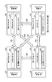
- FIG. 3 shows another example of the configuration in which three processors (first processor 400, third processor 600, and fourth processor 700) and a memory controller 100 incorporating the nonvolatile cache memory 10 are interconnected by QPI or the like.
- processors first processor 400, third processor 600, and fourth processor 700
- memory controller 100 incorporating the nonvolatile cache memory 10 are interconnected by QPI or the like.
- the configuration is shown in which a plurality of processors and a plurality of memory controllers 100 are connected to each other, for example, a scalable computer may be used. System construction is possible.
- the first processor 400 is connected to a first volatile main memory 410 such as a DRAM
- the third processor 600 is connected to a third volatile main memory 610 such as a DRAM
- a fourth volatile main memory 710 such as a DRAM
- the memory controller 10 is connected to a nonvolatile main memory 110 such as an MRAM.
- the first processor 400 includes one or more processor cores 420 that read / write data from / to any main memory (the first volatile main memory 410, the nonvolatile main memory 110, the third volatile main memory 610, and the fourth volatile main memory 710). And a first volatile cache memory 430 for storing a part of data stored in any main memory.
- the third processor 600 includes one or more processor cores 620 that read / write data from / to any main memory, and a third volatile cache memory 630 that stores a part of the data stored in any main memory,
- the fourth processor 700 includes one or more processor cores 720 that read / write data from / to any main memory, and a fourth volatile cache memory 730 that stores a part of the data stored in any main memory. Have A specific configuration of the memory controller 100 will be described later.
- the transaction processing system is also required to have high reliability, the data that guarantees the atomicity of writing to the nonvolatile memory (property that does not end in the middle of writing) and ordering (ordering) by the program executed on the processor.
- a permanent update processing method is required.
- WAL Write Ahead Logging
- shadow page As a method for guaranteeing atomicity, for example, a method for managing multiple versions of data called WAL (Write Ahead Logging) or shadow page is widely known.
- WAL Write Ahead Logging
- the original data stored in the main memory is not updated at first, but the value of the data secured in another area of the main memory is first updated to update the new version of the data.
- the nonvolatile main memory in order to create a new version, the nonvolatile main memory (permanent memory) is transferred. Since access is required, the speed cannot be increased sufficiently.
- the problem in assuring the ordering of writing to the nonvolatile main memory is to adjust the timing of writing to the memory such as various caches, write buffers, and write combine buffers existing between the processor core and the nonvolatile main memory. Volatile memory such as a buffer. Due to this existence, when the processor core writes data by a write instruction, the order of data reaching the nonvolatile main memory is changed, or the data remains in the cache without being immediately written to the nonvolatile main memory. .
- the memory controller 100 incorporating the nonvolatile cache memory 10 and the processor 300 are connected via the interconnect 200 such as QPI, and means for realizing high-speed commit processing while guaranteeing atomicity and ordering. I will provide a.
- the first method uses a cache coherence protocol to transfer data (permanent data) to be committed to a nonvolatile cache memory 10 built in the memory controller 100 at a high speed immediately after the application or the like has written it. It is a means to evict and persist.
- the processor core uses the characteristics of a cache coherence protocol that controls the state of the cache memory of a plurality of processors (processor cores) so that they do not contradict each other.
- the direct write processing in-place update
- the update contents are immediately transferred to the memory controller 100, and the transferred updated data is written to the nonvolatile cache memory 10 and made permanent.
- the memory controller 100 including the non-volatile cache memory 10 is connected to the processor 300 having a cache by an interconnect that guarantees the coherence of both caches using a cache coherence protocol.
- a request request that causes a procedure for sending updated data, determined by a cache coherence protocol, is transferred to the memory controller 100 in order to transfer the written data in the processor 300 to the memory controller 100 side.
- the data is sent to 300 and the sent data is written into the nonvolatile cache memory 10 and made permanent.
- the processor core 320 of the processor 300 attempts to perform in-place update of data (value A) stored in the area (address) X of the nonvolatile main memory 110 without using an explicit multiple version management method.
- Data (value A) stored in the area X is read from the nonvolatile main memory 110, sent to the processor 300 via the interconnect 200 such as QPI, and updated in-place by the processor core 320, the updated data ( The value A ′) is driven out to the memory controller 100 connected to the processor 300 via the interconnect 200 according to the cache coherence protocol.
- the updated data (value A ′) is written into the nonvolatile cache memory 10.
- the pre-update data (value A) still exists on the nonvolatile main memory 110, at this time, as data corresponding to the area X, the data (value A) on the nonvolatile main memory 110 and the nonvolatile cache memory 10 A state in which the above data (value A ′) exists simultaneously can be realized without explicitly creating a plurality of versions in different areas (addresses), and atomicity can be guaranteed. Since multiple versions of persistent data exist on the persistent memory at the same time, the commit process can be completed at this point. In other words, the commit process can be completed simply by writing the updated data to the higher-speed nonvolatile cache memory 10 without writing to the nonvolatile main memory 110, so that a higher-speed commit process is possible.
- the second means is, for example, a memory barrier that confirms completion of writing of updated persistent data (in other words, completion of persistence of updated persistent data) in order to determine completion of transaction commit processing.
- Means As shown in FIG. 4, after executing the memory barrier in the state (b), it is necessary to change to the state (c), and guaranteeing this order is the guarantee of ordering. In general, even if the processor core recognizes that the write processing has been performed, the updated data remains in a volatile memory such as a cache or write buffer between the processor core and the main memory, and at what timing the updated data is Thus, it is difficult for the processor core (that is, the application operating on the processor core) to know whether it has actually been written to the main memory.
- a means for immediately ejecting the updated data to the nonvolatile cache memory 10 built in the memory controller 100 is provided.
- This means plays one of the roles of guaranteeing ordering.
- means for confirming whether the updated data reaches the nonvolatile cache memory 10 and the actual writing process is completed is also necessary.
- the writing process of the data (updated data) that the processor 300 (application) has evicted to the memory controller 10 is completed ( Ordering is guaranteed by providing a means for confirming the completion of persistence.
- the interconnect 200 such as the QPI is designed to be connected to a processor such as an XEON processor. Even if the memory controller 100 and the processor are connected via the interconnect 200, the processor may be connected to the interconnect 200 via the interconnect 200. Assuming that it is the same processor as itself, messages are exchanged according to the cache coherence protocol. Using this, the memory controller 100 obtains updated permanent data and updated timing information from the processor.
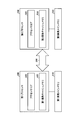
- the information processing apparatus 1 shown in FIG. 1 includes a memory controller 100 to which a nonvolatile main memory 110 is connected, and a processor 300 to which a volatile main memory 310 is connected, and these are connected via an interconnect 200.
- the interconnect 200 is an interconnect that guarantees a protocol (cache coherence protocol) indicating a procedure for preventing data mismatch between a plurality of cache memories, and is configured by, for example, QPI.
- the memory controller 100 and the processor 300 may be connected by a bus or a network.
- the processor 300 is a CPU such as an XEON processor, for example, and operates according to a cache coherence protocol guaranteed by the interconnect 200. As illustrated in FIG. 1, the processor 300 includes one or more processor cores 320 (for convenience of explanation, only one processor core 320 is illustrated) and a volatile cache memory 330.
- the processor core 320 reads / writes data from / to the volatile main memory 310 or the nonvolatile main memory 110.
- the volatile cache memory 330 stores a part of data stored in the volatile main memory 310 or the nonvolatile main memory 110.
- each of the one or more processor cores 320 has a private cache such as an L1 data cache, an L1 instruction cache, and an L2 cache (not shown).
- a last level cache (LLC) which is a cache located at the lowest level in a cache hierarchy such as an L3 cache, is a shared cache shared by the processor cores 320.
- LLC last level cache
- SRAM Static Random Access Memory
- these are referred to as a volatile cache memory 330. The following description is based on such a configuration, but is not limited to this.
- the processor 320 includes a memory controller (not shown) such as a DRAM controller that controls reading and writing of data according to instructions from the processor core 320, and a volatile main memory 310 is connected thereto.
- the last level cache (LLC) or the like may be a non-volatile cache.
- the volatile main memory 310 is a main memory (main storage device) composed of a volatile memory such as a DRAM.
- the main memory connected to the processor 300 may be a volatile memory other than a DRAM, for example, or a non-volatile memory such as an MRAM, for example.
- the memory controller 100 includes a nonvolatile cache memory 10 and a controller 20.
- the nonvolatile cache memory 10 is used for storing a part of data stored in the nonvolatile main memory 110.
- the controller 20 controls memory access such as data writing to and reading from the nonvolatile cache memory 110.
- the processor 300 is connected to the nonvolatile main memory 110 via the memory controller 100.
- the nonvolatile main memory 110 in the present embodiment is configured by MRAM, but is not limited thereto.
- the nonvolatile main memory 110 may be composed of PCM, ReRAM (Resistive Random Acess Memory), FeRAM (Ferroelectric Random Access Memory), Memristor, etc., or NVDIMM (Non-volatile DIMM) combining DRAM and NAND Flash. There may be.
- the nonvolatile main memory 110 may be a volatile memory (DRAM, SRAM, etc.) backed up by a battery (power supply from the battery is continued even when the power is turned off).
- the controller 20 uses the cache coherence protocol guaranteed by the interconnect 200 to detect that the processor 300 has updated the data corresponding to any area of the nonvolatile main memory 110, and then stores the updated data in the memory. The data is transmitted to the controller 100 and the updated data is written to the nonvolatile cache memory 10.
- the controller 20 After receiving a first request for requesting data corresponding to any area of the nonvolatile main memory 110 from the processor 300, the controller 20 receives the data corresponding to the area and the data.
- a first response message including information indicating that the data is held in the nonvolatile cache memory 10 is transmitted to the processor 300 via the interconnect 200.
- the processor 300 (application) It detects that the data corresponding to the area has been updated.
- the cache line is unit information held in the cache memory. For example, the cache line corresponding to a specific area on the nonvolatile main memory 110 is a copy of data corresponding to the specific area.
- the controller 20 even if the controller 20 does not hold the data corresponding to any area of the nonvolatile main memory 110 requested by the first request in the nonvolatile cache memory 10, the controller 20 A first response message including data read from the area and information indicating that the data is held in the nonvolatile cache memory 10 is transmitted to the processor 300.
- the controller 20 After receiving the second request, the controller 20 does not perform the process of invalidating the cache line corresponding to the area, and invalidates the cache line corresponding to the area as a response to the second request.
- a second response message for notifying that it has been set is transmitted to the processor 300 via the interconnect 200.
- the controller 20 transmits a third request for requesting data corresponding to the area to the processor 300 via the interconnect 200, and as a response to the third request, the processor 20 The updated data is received by 300. Then, the controller 20 writes the received updated data in the nonvolatile cache memory 10.
- the third request is information for requesting data corresponding to the area in order to update the data corresponding to the area updated by the processor 300, and the second processor is provided on the memory controller 100 side. This information is transmitted when the second processor fails to refer to the data corresponding to the area (write miss or read miss), assuming that it is connected.
- the controller 20 does not update the updated data received as a response to the third request.
- the controller 20 sends a third request that causes a procedure for sending updated data to the processor 300 and writes the data sent as a response to the third request to the nonvolatile cache memory 10.
- the procedure for sending the updated data is a procedure determined by a protocol (cache coherence protocol) guaranteed by the interconnect 200 in order to transfer the updated data in the processor 300 to the memory controller 100 side. The detailed operation example will be described later.
- the cache coherence protocol guaranteed by the interconnect 200 connecting the processor 300 and the memory controller 100 is a cache coherence protocol such as the QPI protocol or the MESIF protocol guaranteed by the QPI, but is not limited thereto.
- it may be the MSI protocol, the MESI protocol, the MOESI protocol, the MESIF protocol itself, or any protocol obtained by extending or changing them.
- it may be a protocol in which the Owned state of the MOESI protocol is added to the MESIF protocol.
- an existing XEON processor and QPI may be used to design and implement a unique memory controller 100 and connect via QPI.
- cache line states such as Modified state, Exclusive state, Shared state, Invalid state, and Forward state are provided, and the basic operation is QPI. Conforms to protocol and MESIF protocol. Details will be described in the detailed operation examples described later.
- a home node (Home node, for example, a CPU in the case of an XEON processor system) that stores and manages persistent data is arranged to be a node to which the memory controller 100 is connected.
- a program can be set by using an API (Application Program Interface) that specifies the number of a home node that manages persistent data.
- API Application Program Interface
- FIG. 3 when the memory controller 100 is arranged at a position where the second processor 500 may exist in the system configuration of the information processing apparatus and this node is used as a home node, the API has, for example, persistent data.
- the information processing apparatus 1 When a storage area (memory) is secured, a home node number “2” may be designated as an argument of a memory securing function. As a result, the permanent data is arranged in the area X of the nonvolatile main memory 110 as shown in FIG.
- the information processing apparatus 1 only needs to include a setting unit for setting a main memory that is a destination of permanent data.
- An example of this setting means is API.
- persistent data is automatically arranged in the area X of the nonvolatile main memory 110 as shown in FIG. May be.
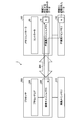
- FIG. 6 is a diagram illustrating an example of processing in which an application updates (permanently) data corresponding to the area X of the nonvolatile main memory 110.
- the processor core 320 application
- the processor core 320 reads the data stored in the area X of the nonvolatile main memory 110 (data indicating the value A in this example) by a read command, caches the data in the volatile cache memory 330, and sets the cache line (
- the value A ′ is written to the first cache line by a write command and updated in place (step S701).
- the updated data (value A ′) written in the volatile cache memory 330 of the processor 300 remains on the volatile cache memory 330 by “means for perpetuating persistent data to the nonvolatile cache memory 10 at a high speed” to be described later.
- the processor core 320 executes a persistence confirmation instruction for confirming whether the persistence of the updated data by the external device (in this example, the memory controller 100) connected via the interconnect 200 is completed. (Step S702).
- the updated data is persisted by the external device (in this example, the memory controller 100) on the processor 300 (application) side by “means for confirming completion of the persistence of persistent data” described later. It is possible to detect (confirm) whether the process has been completed.
- the details of the operations of “means for expelling persistent data to the nonvolatile cache memory 10 and making it permanent” and “means for confirming completion of persistent data” will be described below.
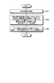
- step S1 of FIG. 7 first, the processor core 320 updates the data (value A) stored in the area X in order to update the data (value A) stored in the area X of the nonvolatile main memory 110. Is stored in the volatile cache memory 330.
- the cache line corresponding to the area X of the nonvolatile main memory 110 may be referred to as a “first cache line”.
- step S ⁇ b> 3 of FIG. 7 the memory controller 100 selects a cache line corresponding to the area X of the nonvolatile main memory 110 among the cache lines of the nonvolatile cache memory 10 (referred to as “second cache line”). If it behaves so as to write to (has not actually written) (step S3-1), the processor 300 drives the updated data to the memory controller 100 (step S3-2). Then, the memory controller 100 writes the updated data (data corresponding to the region X) received from the processor 300 to the nonvolatile cache memory 10.
- FIG. 8 is a diagram showing an example of a detailed procedure of each step (S1 to S3) in FIG. First, the contents corresponding to step S1 will be described.
- the processor core 320 designates the address of the area X of the nonvolatile main memory 110 and executes a read command for reading the data stored in the area X
- the volatile cache memory 330 corresponds to the area X. Since the cache line to be cached is in an INVALID state in which the cache line is not cached, a cache miss occurs, and the cache node first snoop request (requests data corresponding to the region X) to the home node at the address of the region X Information).
- the first snoop request corresponds to the first request described above.
- the memory controller 100 of the present embodiment is connected to the position of the home node instead of the processor, and the first snoop request arrives at the memory controller 100 (if there are other processors, they are sent to them). Also arrives).
- the second processor reads the cache line containing the data (value A) stored in the area X of the nonvolatile main memory 110 from the nonvolatile main memory 110 and transfers it to the processor 300 via the interconnect 200. Then, the processor 300 stores the transferred cache line (cache line corresponding to the area X) in the volatile cache memory (last level cache) 330.
- the cache line (first cache line) corresponding to the area X is not changed when the contents of the cache line are read from the nonvolatile main memory 110, and the cache of any other processor The memory enters an exclusive state in which no cache line of the same address is entered.
- the first cache line of the processor 300 is a shared state in which the other processors are also caching the cache line corresponding to the region X, or other processors are also If the cache line corresponding to the area X is cached and if the cache line corresponding to the area X is requested, the forward state is reached, which is the state in which a response can be made only by transferring a copy. It is aimed to control from the memory controller 100. Therefore, when the first snoop request arrives, the controller 20 of the memory controller 100 behaves as if the cache line corresponding to the area X is in the exclusive state or the forward state, and the cache corresponding to the area X is cached.
- the controller 20 since the cache line corresponding to the area X is not actually cached in the nonvolatile cache memory 10 of the memory controller 100, the controller 20 reads the data stored in the area X of the nonvolatile main memory 110. Information indicating that the data corresponding to the area X is cached together with the data read from the area X (not actually cached) ) To the processor 300.
- the processor 300 that has received the first response message determines that the processor (second processor) connected via the interconnect 200 holds a cache line corresponding to the region X.
- the included cache line is held in the volatile cache memory 330 as the first cache line.
- the processor core 320 can read the data (value A) stored in the area X.
- the first cache line of the processor 300 is in the forward state, and there is a processor (second processor) connected via the interconnect 200 from the processor 300 (the memory controller actually exists). 100), the cache line corresponding to the region X (second cache line) among the cache lines of the second processor is seen to be in the Shared state.
- the processor core 320 writes the data corresponding to the area X with a write instruction (designates the address of the area X and executes the write instruction). Since the cache line (first cache line) corresponding to the region X exists in the volatile cache memory 330, the value A ′ is written to the first cache line.
- the processor 300 uses the cache coherence protocol. Based on this, an invalidate request for requesting to invalidate the cache line corresponding to the region X is broadcast to other processors. This invalidate request corresponds to the second request described above.
- the reason why the memory controller 100 controls the first cache line to be in the forward state is to cause this invalidate request. That is, when the invalidate request is issued, the memory controller 100 can know that a write command for updating data corresponding to the region X is executed. If there is a second processor that operates in accordance with the cache coherence protocol instead of the memory controller 100, when the second processor receives the invalidation request, the second processor needs to perform the invalidation processing of the cache line according to the request. is there.
- the memory controller 100 is an invalidate request that is intentionally issued using the cache coherence protocol in order to know the update timing of data corresponding to the region X. The controller 100 does not necessarily need to actually perform the invalidation process.
- the controller 20 of the memory controller 100 behaves as if the cache line corresponding to the region X is invalidated according to the cache coherence protocol as a response to the invalidate request without performing the invalidation process. Therefore, a second response message for notifying the invalidation is returned to the processor 300.
- the memory controller 100 can know the update timing of data corresponding to the region X.
- the processor 300 that has received the second response message that is a response to the invalidate request determines that the cache line (cache line corresponding to the region X) of the same address possessed by another processor has been invalidated, and the first An actual write process is performed on the cache line, and the state of the first cache line is changed to the Modified state.
- step S3 the contents corresponding to step S3 will be described.
- the controller 20 of the memory controller 100 returns a second response message that is a response to the invalidate request and assumes that the second processor exists instead of the memory controller 100
- the second processor executes the second cache.
- a second snoop request (information requesting data corresponding to the region X) due to a write miss is sent when writing to the line fails. The purpose of this is to immediately draw the data corresponding to the area X updated by the processor 300 in step S2 to the memory controller 100 side via the interconnect 200.
- the second snoop request corresponds to the above-described third request.
- the processor 300 Upon receiving the second snoop request, the processor 300 transmits a third response message including the updated data (value A ′) of the first cache line as a response to the second snoop request, and puts the first cache line in the INVALID state. Change to If there is a second processor instead of the memory controller 100, when the second processor receives a third response message that is a response to the second snoop request, the data (value) included in the third response message is received. The content of the nonvolatile main memory 110 is updated in A ′). Here, the memory controller 100 immediately draws data corresponding to the area X updated by the processor 300 to the memory controller 100 side via the interconnect 200.
- the contents of the nonvolatile main memory 110 are not updated with the updated data (value A ′) included in the third response message (write miss is not performed). Caused but not the light itself).
- the controller 20 of the memory controller 100 writes this data into the nonvolatile cache memory 10. More specifically, for example, the data is written in an area in the nonvolatile cache memory 10 where the second cache line is held (an area corresponding to the area X in the nonvolatile cache memory 10).
- the data corresponding to the area X updated by the processor 300 is written in the nonvolatile cache.
- the old version indicating the value A and the latest version indicating the value A ′ exist as data corresponding to the area X, and the commit process can be completed.
- the information processing apparatus 1 reads the first data (for example, data (value A) stored in the area X) on the nonvolatile main memory 110 to the processor 300 and updates the updated data (value A ′). ) Is stored in the nonvolatile cache memory 10 as the second data, the commit process for making the data permanent is completed.
- FIG. 9 is a flowchart showing an operation example of the controller 20 of the memory controller 100 described above.
- the controller 20 receives the first snoop request from the processor 300, the controller 20 transmits the first response message as a response to the first snoop request to cause the processor to issue the invalidate request (step S901). ).
- the controller 20 detects that the data requested by the above-described first snoop request has been updated on the processor 300 side. Then, the controller 20 does not actually perform the invalidation process, and transmits the above-described second response message as a response to the invalidate request (step S902).
- the controller 20 transmits the second snoop request described above to the processor 300 in order to immediately draw updated data to the memory controller 100 side (step S903).
- the controller 20 writes the data (data corresponding to the region X updated by the processor 300) included in the third response message received as a response to the second snoop request in the nonvolatile cache memory 10 (step S904). ).
- a second snoop request due to a read miss may be sent.
- the processor 300 After sending the third response message as a response to the second snoop request described above, the processor 300 sends a third due to a read miss sent when an attempt to read the first cache line fails as shown in FIG. Send a snoop request (information requesting data (cache line) corresponding to area X).
- the processor 300 sends a snoop request (information requesting data (cache line) corresponding to area X).
- the processor 300 sends a third due to a read miss sent when an attempt to read the first cache line fails as shown in FIG.
- Send a snoop request (information requesting data (cache line) corresponding to area X).
- the third snoop request is issued, and the issued third snoop request arrives at the memory controller 100 via the interconnect 200.
- the controller 10 that has received the third snoop request receives the third snoop request after the data (value A ′) included in the third response message has been written to the nonvolatile cache memory 10 (that is, after the persistence has been completed).
- a fourth response message including data indicating the value A ′ is transmitted.
- the processor 300 receives the fourth response message, the first cache line enters, for example, the Shared state, and when the reading of the data indicating the value A ′ is completed, the memory controller 100 guarantees that the persistent data has been persisted. As a result, the commit process can be completed.
- the processor 300 of the present embodiment is the data corresponding to any region X of the nonvolatile main memory 110 updated by the processor 300 from the external device (here, the memory controller 100) connected via the interconnect 200.
- a protocol a cache coherence protocol guaranteed by the interconnect 200
- a third request (in this example, the above-described second snoop request) that requests data corresponding to the region X to refer to
- a confirmation request for confirming that the transmitted data has been completed is sent to the external device.
- the third snoop request is described as an example of the confirmation request, but the present invention is not limited to this.
- this embodiment implements Intel's Pcommit command for checking memory write persistence in the non-patent literature “CHAPTER 11: MEMORY -02 INSTRUCTIONS” of “Intel Architecture Instruction Extensions Programming Reference (319433-022, OCTOBER 2014)”. In this case, it can be realized by a method as shown in FIG.
- FIG. 12 is a flowchart showing an operation example of the information processing apparatus 1 when confirming the completion of the persistence of the persistent data.
- the processor 300 transmits the above-described third snoop request as a response to the above-described second snoop request, and then transmits the above-described third snoop request to the memory controller 100 via the interconnect 200 (step S1201).
- the controller 20 of the memory controller 100 that has received the third snoop request, the non-volatile cache memory 10 of the data (value A ′) included in the third response message received from the processor 300 before receiving the third snoop request.
- the above fourth response message is transmitted to the processor 300 via the interconnect 200 (step S1202).
- step S1203 When the processor 300 having received the fourth response message completes the reading of the data (value A ′) from the first cache line that is ready to be read, the data that has been expelled from the volatile cache memory 330 to the memory controller 100 (described above). It is confirmed that the perpetuation of the data included in the third response message has been completed (step S1203).
- the third response message after transmitting the third response message as a response to the second snoop request, it waits for a predetermined fixed time of several cycles to several tens of cycles.
- the certain time is the sum of the time required to send data from the processor 300 to the memory controller 100 and the time required for the memory controller 100 to complete the process of writing data into the nonvolatile cache memory 10 (permanent). Is a longer time.
- This time is a value determined in advance at the time of measurement or design and provided to an application or the like.
- This method can be similarly applied to a second embodiment described later. Further, the above-described Pcommit instruction may be implemented by this method, and the same applies to the second embodiment described later.
- the memory controller 100 is connected to the processor 300 via the interconnect 200 that guarantees the cache coherence protocol indicating the procedure for preventing data mismatch between the plurality of cache memories. Connected. Then, the controller 20 of the memory controller 100 uses the cache coherence protocol guaranteed by the interconnect 200, and the processor 300 updates data corresponding to any region X of the nonvolatile main memory 110 connected to the memory controller 100. After detecting this, the updated data is transmitted to the memory controller 100, and the updated data received from the processor 300 is written into the nonvolatile cache memory 10.
- the data on the nonvolatile main memory 110 and the data on the nonvolatile cache memory 10 simultaneously exist as data corresponding to the region X.
- the state can be realized without explicitly creating multiple versions, and atomicity can be guaranteed.
- the commit process can be completed simply by writing the updated data to the nonvolatile cache memory 10 without writing the nonvolatile main memory 110, so that a faster commit process is possible.
- the processor 300 uses the data corresponding to the area X to refer to the data corresponding to the area X of the nonvolatile main memory 110 updated by the processor 300 from the memory controller 300.
- the processor 300 After transmitting the data corresponding to the area X out of the data stored in the volatile cache memory 330 as a response based on the protocol for the third request (in this example, the second snoop request described above) (in this example, Then, after transmitting the above-mentioned third response message, a confirmation request (in this example, the above-mentioned third snoop request) for confirming that the transmitted data has been completed is transmitted, and a response to the confirmation request is sent. To confirm that the transmitted data has been persisted.
- the processor 300 when the processor 300 updates the persistent data using the cache coherence protocol, the updated data is immediately ejected to the nonvolatile cache memory 10 built in the memory controller 100.
- the ordering is guaranteed by the processor 300 providing a means for confirming the completion of the persistence of the data (updated data) evicted to the memory controller 100.
- high-speed commit processing can be realized while ensuring atomicity and ordering. Therefore, a high-performance and highly reliable data perpetuation processing method can be realized.
- a cache line is used as a unit for obtaining coherence.
- the present invention is not limited to this.
- the granularity may be any granularity such as an OS page unit or a block unit.
- the processor 300 is not limited to the CPU but may be an accelerator such as a GPU. The same applies to a second embodiment described later.
- the processor 300 and the memory controller 100 are different from the existing cache coherence protocol in a cache coherence protocol optimized for commit processing (hereinafter referred to as “optimization protocol”).
- optimization protocol a cache coherence protocol optimized for commit processing
- This is different from the above-described first embodiment in that it is connected via an interconnect 800 that guarantees the The interconnect 800 ensures an optimization protocol for maintaining consistency between the volatile cache memory 330 of the processor 300 and the non-volatile cache memory 10 of the memory controller 100.
- the basic configuration of the processor 300 and the memory controller 100 is the same as that of the first embodiment, but the processor 300 and the memory controller 100 operate according to an optimization protocol.
- step S11 of FIG. 13 first, the processor 300 reads the data stored in the area X and updates the volatile cache in order to update the data (value A) stored in the area X of the nonvolatile main memory 110. Save in the memory 330. More specifically, it is as follows.
- the processor core 320 designates the address of the area X of the nonvolatile main memory 110 and executes a read command for reading the data (value A) stored in the area X
- the volatile cache memory 330 Since the cache line corresponding to the area X is in the INVALID state where the cache line is not cached, a cache miss occurs and the home node (memory controller 100 in this example) having the address of the area X corresponds to the area X.
- a fourth request for data is sent.
- the controller 20 of the memory controller 100 reads the data (value A) stored in the area X of the nonvolatile main memory 110 and caches it in the nonvolatile cache memory 10 (caches the second cache line). .
- the controller 20 sends a fifth response message including the cache line corresponding to the area X (the contents of the second cache line including the data (value A) read from the area X) to the processor 300.
- the processor core 320 of the processor 300 that has received the fifth response message holds the cache line included in the fifth response message in the volatile cache memory 330 as the first cache line.
- the processor core 320 can read the data (value A) stored in the area X.
- the state of the first cache line becomes a state (FORWARD TO HOMENODE) in which the writing contents are transferred to the home node when the writing to make the next permanent is performed.
- step S ⁇ b> 12 of FIG. 13 the processor 300 (application) updates the data stored in the first cache line by writing the value A ′ to the first cache line with a write instruction. Then, the updated data is expelled to the memory controller 100. More specifically, it is as follows. First, the processor core 320 writes the data corresponding to the area X with a write instruction (designates the address of the area X and executes the write instruction). Since the cache line (first cache line) corresponding to the region X exists in the volatile cache memory 330, the value A ′ is written to the first cache line.
- the state of the first cache line is “FORWARD TO HOMENODE”
- the content written to the first cache line is immediately transferred from the volatile cache memory 330 to the memory controller 100.
- the state of the first cache line becomes the INVALID state.
- the controller 20 of the memory controller 100 writes the updated data received from the processor 300 in the nonvolatile cache memory 10. More specifically, the controller 20 writes and reflects the updated copy of the first cache line received from the processor 300 in the second cache line.
- the nonvolatile main memory 110 is not updated.
- the data corresponding to the region X the old version indicating the value A and the latest version indicating the value A ′ exist at the same time, and the commit process can be completed.
- FIG. 14 is a flowchart showing an operation example of the information processing apparatus 1 described above. The specific contents of each step are as described above.
- the processor core 320 of the processor 300 transmits the above-described fourth request to the memory controller 100 via the interconnect 800 (step S1301).
- the controller 20 of the memory controller 100 that has received the fourth request caches the second cache line and returns the above-described fifth response message as a response to the fourth request (step S1302).
- the processor core 320 of the processor 300 that has received the fifth response message caches the cache line (contents of the second cache line) included in the fifth response message as the first cache line (step S1303).
- the processor core 320 executes writing to the first cache line (step S1304), and transfers updated data (a copy of the updated first cache line) to the memory controller 100 via the interconnect 800. (Step S1305).
- the controller 20 of the memory controller 100 writes and reflects the updated data received from the processor 300 via the interconnect 800 in the second cache line (step S1306).
- the processor 300 and the memory controller 100 are connected via the interconnect 800 that guarantees the above-described optimization protocol.
- the processor 300 updates data corresponding to any region X of the nonvolatile main memory 110
- the updated data is transferred to the memory controller 100 according to the above-described optimization protocol.
- the received updated data is written into the nonvolatile cache memory 10.
- the processor core 320 (application) transfers the write contents for the first cache line to the memory controller 100 as described above, the processor core 320 (application) sends a confirmation request for confirming the completion of the persistence of the transferred data to the interconnect 800. To the memory controller 100, and based on the response to the confirmation request, it is confirmed that the transferred data has been made permanent. In this example, the processor core 320 attempts to read the first cache line after transferring the write contents for the first cache line to the memory controller 100, fails, and the fifth request (area) sent when the read fails. Data corresponding to X (information requesting a cache line) is sent.
- a fifth request is issued, and the issued fifth request arrives at the memory controller 100 via the interconnect 800.
- the controller 10 that has received the fifth request has completed writing of the data (value A ′) corresponding to the updated area X received from the processor 300 before receiving the fifth request to the nonvolatile cache memory 10. Later (that is, after the persistence is completed), a sixth response message including data indicating the value A ′ is transmitted as a response to the fifth request.
- the processor 300 receives the sixth response message, the first cache line becomes ready to be read, and by completing the reading of the data indicating the value A ′, the memory controller 100 can make the persistent data persistent. Since the completion is guaranteed, the commit process can be completed.
- the area X is used for confirmation of persistence.
- the present invention is not limited to this.
- an area different from the area X may be used for confirmation. In this case, there is no need for the process of changing the state of the first cache line performed after transferring the write contents to the first cache line to the memory controller 100 to the INVALID state.
- FIG. 15 is a flowchart illustrating an operation example of the information processing apparatus 1 when confirming the completion of the persistence of persistent data.
- the processor 300 After transferring the contents written to the first cache line to the memory controller 100 as described above, the processor 300 transmits the above-described fifth request to the memory controller 100 via the interconnect 800 (step S1401).
- the controller 20 of the memory controller 100 that has received the fifth request, the non-volatile cache memory of the data (value A ′) corresponding to the updated region X received from the processor 300 before receiving the fifth request.
- the sixth response message described above is transmitted to the processor 300 via the interconnect 800 (step S1402).
- step S1403 When the processor 300 having received the sixth response message completes the reading of the data (value A ′) from the first cache line that is ready to be read, the data that has been evicted from the volatile cache memory 330 to the memory controller 100 (updated) It is confirmed that the perpetuation of the data corresponding to the area X is completed (step S1403).
- the fifth request described above As another method for confirming the completion of the persistence of the persistent data, as described in the first embodiment above, after the write content to the first cache line is transferred to the memory controller 100, the fifth request described above is performed. Instead of transmitting, a method of confirming persistence by waiting for a certain time may be applied.
Landscapes
- Engineering & Computer Science (AREA)
- Theoretical Computer Science (AREA)
- Physics & Mathematics (AREA)
- General Engineering & Computer Science (AREA)
- General Physics & Mathematics (AREA)
- Human Computer Interaction (AREA)
- Memory System Of A Hierarchy Structure (AREA)
Abstract
La présente invention vise à réaliser un procédé de perpétuation de données de haute performance et très fiable. Un dispositif de commande de mémoire d'un mode de réalisation comprend une mémoire cache non volatile et un dispositif de commande. La mémoire cache non volatile mémorise en son sein une partie des données mémorisées dans une mémoire principale non volatile conectée au dispositif de commande de mémoire. Le dispositif de commande commande l'écriture dans la mémoire cache non volatile. Le dispositif de commande de mémoire est raccordé à un dispositif de traitement par le biais d'un interconnecteur qui garantit un protocole indiquant une procédure permettant d'empêcher une incohérence de données parmi une pluralité de mémoires caches. Après avoir détecté que des données mémorisées dans une région quelconque de la mémoire principale non volatile ont été mises à jour par le dispositif de traitement, le dispositif de commande transmet les données mises à jour au dispositif de commande de mémoire et écrit les données mises à jour dans la mémoire cache non volatile en utilisant le protocole.
Priority Applications (3)
| Application Number | Priority Date | Filing Date | Title |
|---|---|---|---|
| PCT/JP2015/070438 WO2017010004A1 (fr) | 2015-07-16 | 2015-07-16 | Dispositif de commande de mémoire, dispositif de traitement d'informations et dispositif de traitement |
| JP2017528259A JP6334824B2 (ja) | 2015-07-16 | 2015-07-16 | メモリコントローラ、情報処理装置および処理装置 |
| US15/869,287 US10635587B2 (en) | 2015-07-16 | 2018-01-12 | Memory controller, information processing apparatus, and processor |
Applications Claiming Priority (1)
| Application Number | Priority Date | Filing Date | Title |
|---|---|---|---|
| PCT/JP2015/070438 WO2017010004A1 (fr) | 2015-07-16 | 2015-07-16 | Dispositif de commande de mémoire, dispositif de traitement d'informations et dispositif de traitement |
Related Child Applications (1)
| Application Number | Title | Priority Date | Filing Date |
|---|---|---|---|
| US15/869,287 Continuation US10635587B2 (en) | 2015-07-16 | 2018-01-12 | Memory controller, information processing apparatus, and processor |
Publications (1)
| Publication Number | Publication Date |
|---|---|
| WO2017010004A1 true WO2017010004A1 (fr) | 2017-01-19 |
Family
ID=57757275
Family Applications (1)
| Application Number | Title | Priority Date | Filing Date |
|---|---|---|---|
| PCT/JP2015/070438 Ceased WO2017010004A1 (fr) | 2015-07-16 | 2015-07-16 | Dispositif de commande de mémoire, dispositif de traitement d'informations et dispositif de traitement |
Country Status (3)
| Country | Link |
|---|---|
| US (1) | US10635587B2 (fr) |
| JP (1) | JP6334824B2 (fr) |
| WO (1) | WO2017010004A1 (fr) |
Cited By (2)
| Publication number | Priority date | Publication date | Assignee | Title |
|---|---|---|---|---|
| GB2549572A (en) * | 2016-04-22 | 2017-10-25 | Advanced Risc Mach Ltd | Caching data from a non-volatile memory |
| US10761843B2 (en) | 2017-07-28 | 2020-09-01 | Fujitsu Limited | Information processing device and information processing method |
Families Citing this family (4)
| Publication number | Priority date | Publication date | Assignee | Title |
|---|---|---|---|---|
| US11132145B2 (en) | 2018-03-14 | 2021-09-28 | Apple Inc. | Techniques for reducing write amplification on solid state storage devices (SSDs) |
| KR102446121B1 (ko) * | 2018-06-29 | 2022-09-22 | 주식회사 멤레이 | 메모리 제어 장치 및 이를 포함하는 메모리 시스템 |
| US10705957B1 (en) * | 2018-12-19 | 2020-07-07 | International Business Machines Corporation | Selectively updating a coherence state in response to a storage update |
| US10733102B2 (en) * | 2018-12-19 | 2020-08-04 | International Business Machines Corporation | Selectively updating a coherence state in response to a storage update |
Citations (1)
| Publication number | Priority date | Publication date | Assignee | Title |
|---|---|---|---|---|
| WO2014142908A1 (fr) * | 2013-03-14 | 2014-09-18 | Hewlett-Packard Development Company, L.P. | Hiérarchie de mémoire non volatile multiversion pour mémoire persistante |
Family Cites Families (5)
| Publication number | Priority date | Publication date | Assignee | Title |
|---|---|---|---|---|
| US7389308B2 (en) | 2003-05-30 | 2008-06-17 | Microsoft Corporation | Shadow paging |
| US8019937B2 (en) * | 2004-07-21 | 2011-09-13 | Infortrend Technology, Inc. | Applying storage device commit-cached-data-to-media functionality to improve data security in systems that allow storage devices to cache writes |
| US20080183972A1 (en) * | 2007-01-26 | 2008-07-31 | James Norris Dieffenderfer | Snoop Filtering Using a Snoop Request Cache |
| KR101717644B1 (ko) * | 2009-09-08 | 2017-03-27 | 샌디스크 테크놀로지스 엘엘씨 | 고체-상태 저장 디바이스 상에서 데이터를 캐싱하는 장치, 시스템, 및 방법 |
| US9690710B2 (en) * | 2015-01-15 | 2017-06-27 | Qualcomm Incorporated | System and method for improving a victim cache mode in a portable computing device |
-
2015
- 2015-07-16 WO PCT/JP2015/070438 patent/WO2017010004A1/fr not_active Ceased
- 2015-07-16 JP JP2017528259A patent/JP6334824B2/ja active Active
-
2018
- 2018-01-12 US US15/869,287 patent/US10635587B2/en active Active
Patent Citations (1)
| Publication number | Priority date | Publication date | Assignee | Title |
|---|---|---|---|---|
| WO2014142908A1 (fr) * | 2013-03-14 | 2014-09-18 | Hewlett-Packard Development Company, L.P. | Hiérarchie de mémoire non volatile multiversion pour mémoire persistante |
Non-Patent Citations (1)
| Title |
|---|
| SAYURI SHIOHIRA: "Tomaranai Server o Jitsugen suru Intel Itanium no Technology", MONTHLY ASCII. TECHNOLOGIES, vol. 15, no. 9, 24 July 2010 (2010-07-24), pages 50 - 61 * |
Cited By (4)
| Publication number | Priority date | Publication date | Assignee | Title |
|---|---|---|---|---|
| GB2549572A (en) * | 2016-04-22 | 2017-10-25 | Advanced Risc Mach Ltd | Caching data from a non-volatile memory |
| US10120808B2 (en) | 2016-04-22 | 2018-11-06 | Arm Limited | Apparatus having cache memory disposed in a memory transaction path between interconnect circuitry and a non-volatile memory, and corresponding method |
| GB2549572B (en) * | 2016-04-22 | 2019-11-13 | Advanced Risc Mach Ltd | Caching data from a non-volatile memory |
| US10761843B2 (en) | 2017-07-28 | 2020-09-01 | Fujitsu Limited | Information processing device and information processing method |
Also Published As
| Publication number | Publication date |
|---|---|
| US20180136849A1 (en) | 2018-05-17 |
| JP6334824B2 (ja) | 2018-05-30 |
| US10635587B2 (en) | 2020-04-28 |
| JPWO2017010004A1 (ja) | 2017-12-28 |
Similar Documents
| Publication | Publication Date | Title |
|---|---|---|
| JP6334824B2 (ja) | メモリコントローラ、情報処理装置および処理装置 | |
| US9170946B2 (en) | Directory cache supporting non-atomic input/output operations | |
| US9501425B2 (en) | Translation lookaside buffer management | |
| TWI432963B (zh) | 加速器之低成本快取一致 | |
| US10157133B2 (en) | Snoop filter for cache coherency in a data processing system | |
| TWI526829B (zh) | 電腦系統、用於存取儲存裝置之方法及電腦可讀儲存媒體 | |
| CN105339908B (zh) | 用于支持持久存储器的方法和装置 | |
| CN103744799B (zh) | 一种内存数据访问方法、装置和系统 | |
| US20170192886A1 (en) | Cache management for nonvolatile main memory | |
| US12189545B2 (en) | System, apparatus and methods for handling consistent memory transactions according to a CXL protocol | |
| JP7010809B2 (ja) | デデュープ可能なメモリキャッシュ及びそのための動作方法 | |
| CN111656332B (zh) | 基于本地代理的高速缓存传送加速方案 | |
| CN107408079A (zh) | 带有一致单元的多级别系统存储器的存储器控制器 | |
| US10877890B2 (en) | Providing dead-block prediction for determining whether to cache data in cache devices | |
| US11126564B2 (en) | Partially coherent memory transfer | |
| US12332786B2 (en) | Tracking memory modifications at cache line granularity | |
| CN112673358A (zh) | 在基于区域的高速缓存目录方案中加速对私有区域的访问 | |
| TW201447748A (zh) | 處理裝置 | |
| JP7681005B2 (ja) | プロデューサからコンシューマへのアクティブな直接キャッシュ転送 | |
| TWI506537B (zh) | 使用反射記憶體實行同調之技術 | |
| JP6565729B2 (ja) | 演算処理装置、制御装置、情報処理装置及び情報処理装置の制御方法 | |
| US20230418758A1 (en) | Tag processing for external caches | |
| JP2009223511A (ja) | キャッシュメモリシステム、データ処理装置および記憶装置 |
Legal Events
| Date | Code | Title | Description |
|---|---|---|---|
| 121 | Ep: the epo has been informed by wipo that ep was designated in this application |
Ref document number: 15898316 Country of ref document: EP Kind code of ref document: A1 |
|
| ENP | Entry into the national phase |
Ref document number: 2017528259 Country of ref document: JP Kind code of ref document: A |
|
| NENP | Non-entry into the national phase |
Ref country code: DE |
|
| 122 | Ep: pct application non-entry in european phase |
Ref document number: 15898316 Country of ref document: EP Kind code of ref document: A1 |