WO2017010134A1 - Dispositif de conversion de puissance et son procédé de commande - Google Patents
Dispositif de conversion de puissance et son procédé de commande Download PDFInfo
- Publication number
- WO2017010134A1 WO2017010134A1 PCT/JP2016/061990 JP2016061990W WO2017010134A1 WO 2017010134 A1 WO2017010134 A1 WO 2017010134A1 JP 2016061990 W JP2016061990 W JP 2016061990W WO 2017010134 A1 WO2017010134 A1 WO 2017010134A1
- Authority
- WO
- WIPO (PCT)
- Prior art keywords
- voltage side
- conversion efficiency
- dead time
- appropriate
- switching element
- Prior art date
- Legal status (The legal status is an assumption and is not a legal conclusion. Google has not performed a legal analysis and makes no representation as to the accuracy of the status listed.)
- Ceased
Links
Images






Classifications
-
- H—ELECTRICITY
- H02—GENERATION; CONVERSION OR DISTRIBUTION OF ELECTRIC POWER
- H02M—APPARATUS FOR CONVERSION BETWEEN AC AND AC, BETWEEN AC AND DC, OR BETWEEN DC AND DC, AND FOR USE WITH MAINS OR SIMILAR POWER SUPPLY SYSTEMS; CONVERSION OF DC OR AC INPUT POWER INTO SURGE OUTPUT POWER; CONTROL OR REGULATION THEREOF
- H02M3/00—Conversion of DC power input into DC power output
- H02M3/22—Conversion of DC power input into DC power output with intermediate conversion into AC
- H02M3/24—Conversion of DC power input into DC power output with intermediate conversion into AC by static converters
- H02M3/28—Conversion of DC power input into DC power output with intermediate conversion into AC by static converters using discharge tubes with control electrode or semiconductor devices with control electrode to produce the intermediate AC
Definitions
- the present invention relates to a power converter including a bridge circuit configured using a plurality of switching elements and a control method thereof.
- a loss that occurs during power conversion in a power conversion device using a switching element is a loss caused by a resistance component inside the power conversion device (referred to as “conduction loss”) and switching of the switching element. It is roughly divided into losses caused by operation (called “switching losses”). Of these, the conduction loss is greatly reduced when the current is reduced, but the switching loss is not reduced to the extent that the current is reduced. For this reason, in the power conversion device using a switching element, the switching loss becomes dominant at the time of light load, and this has caused the conversion efficiency to decrease.
- a rectifying unit including an element is provided, and rectification is performed based on one or both of an input value (input voltage or input current) to the switch circuit and an output value (output voltage or output current) from the switch circuit.
- Part (two switching elements) is configured to perform on / off control. With this configuration, the efficiency at the time of light load can be improved as compared with the conventional case.
- the switching power supply device described in Patent Document 1 has a capacitance value of at least one of the capacitive elements constituting the resonance circuit in order to make the characteristics of the resonance circuit appropriate according to the load of the output circuit. Is changed according to the load of the output circuit.
- there is a limit to the number of capacitors (number of stages) whose connection is switched in order to change the capacitance value and it is difficult to finely adjust the capacitance value according to the load to optimize the characteristics of the resonance circuit.
- due to variations in characteristics of the capacitors and aging it may be difficult to make the characteristics of the resonance circuit appropriate.
- the power conversion device described in Patent Document 2 controls on / off of a rectifier (switching element) based on voltage and current information input and output by the switch circuit in order to improve efficiency at light loads. Is done.
- a fixed value ⁇ is set as a time during which both the high-voltage side and low-voltage side switching elements connected in series in the switch circuit are turned off, that is, a dead time, the switching elements in the switch circuit due to load fluctuations are set. It is not possible to sufficiently suppress the occurrence of switching loss due to voltage and current waveform changes. As a result, it is difficult to maintain a sufficiently high conversion efficiency while suppressing a decrease in conversion efficiency due to load fluctuations.
- an object of the present invention is to provide a power conversion device and a control method thereof that can sufficiently suppress a decrease in conversion efficiency due to load fluctuations even if the characteristics of circuit elements vary or change.
- a first aspect of the present invention is a power conversion device that generates an output voltage to be supplied to a load unit from an input DC voltage applied between a high-voltage side input terminal and a low-voltage side input terminal,
- a switch circuit including a first pair of switching elements, which includes a first high-voltage side switching element and a first low-voltage side switching element connected in series to each other, and is connected between the high-voltage side input terminal and the low-voltage side input terminal; , A controller for controlling on / off of the first high-voltage side switching element and the first low-voltage side switching element;
- An input side measurement circuit for obtaining input power applied via the high voltage side input terminal and the low voltage side input terminal;
- An output side measurement circuit for obtaining output power supplied to the load unit,
- the controller is A conversion efficiency calculator that calculates the conversion efficiency of the power converter based on the measurement results of the input side measurement circuit and the output side measurement circuit; By monitoring the conversion efficiency calculated by the conversion efficiency calculation unit while changing the dead time during which
- the appropriate dead time search control unit determines the increase or decrease in the conversion efficiency while sequentially increasing the dead time from a predetermined initial value, so that the conversion efficiency is maximized. Time is obtained as the appropriate dead time.
- the conversion efficiency calculation unit calculates conversion efficiency based on the measurement results of the input side measurement circuit and the output side measurement circuit, and determines the conversion efficiency lower limit value according to the load based on the measurement result of the output side measurement circuit.
- the appropriate dead time search control unit executes the appropriate dead time search process when the calculated conversion efficiency is smaller than the determined conversion efficiency lower limit value.
- the control unit monitors the conversion efficiency calculated by the conversion efficiency calculation unit while changing the switching frequency of the first high-voltage side switching element and the first low-voltage side switching element within a predetermined range.
- An appropriate frequency search control unit for executing an appropriate frequency search process for obtaining the switching frequency at which the efficiency is maximized as an appropriate switching frequency;
- the control signal generator is configured to turn on / off the first high-voltage side switching element and the first low-voltage side switching element at the appropriate frequency. A first switching control signal is generated.
- the frequency search control unit determines the increase or decrease of the conversion efficiency while sequentially decreasing the switching frequency from a predetermined initial value, thereby determining the switching frequency at which the conversion efficiency is maximized. It is obtained as an appropriate switching frequency.
- a sixth aspect of the present invention is the fourth aspect of the present invention.
- the conversion efficiency calculation unit calculates conversion efficiency based on the measurement results of the input side measurement circuit and the output side measurement circuit, and determines the conversion efficiency lower limit value according to the load based on the measurement result of the output side measurement circuit.
- the appropriate frequency search control unit performs the appropriate frequency search process when the calculated conversion efficiency is smaller than the determined conversion efficiency lower limit value.
- the soft switching is performed in each switching element in the switch circuit by the capacitance between both ends of each switching element in the switch circuit and the inductance in the path of the current flowing through each switching element in the switch circuit. It is further characterized by further comprising a resonant circuit.
- An eighth aspect of the present invention is a power conversion device operating as a DC-DC converter according to the first to seventh aspects of the present invention, A transformer, A rectifier circuit connected to the secondary side of the transformer and outputting a DC voltage as the output voltage;
- the switch circuit is A second switching element pair comprising a second high-voltage side switching element and a second low-voltage side switching element connected in series with each other and connected in parallel with the first switching element pair; Connected to the primary side of the transformer as an inverter;
- the control signal generator is When an appropriate dead time is obtained by the appropriate dead time search process, a second switching control signal for turning on and off the second high voltage side switching element and the second low voltage side switching element at the appropriate dead time is further provided.
- Generate and The first and second high-voltage side switching elements and the first and second low-voltage side switching elements are turned on / off at the appropriate frequency when an appropriate switching frequency is obtained by the appropriate frequency search process.
- the first and second switching control signals are generated.
- a ninth aspect of the present invention is the eighth aspect of the present invention.
- the control unit uses the first high-voltage side switching element and the first low-voltage side switching element as fixed side switching elements as a reference, and the second high-voltage side switching element and the second low-voltage side switching as shift-side switching elements. Controlling on / off of the first high-voltage side, the first low-voltage side, the second high-voltage side, and the second low-voltage side switching element by a phase shift method so as to form a switching phase difference with the element.
- a tenth aspect of the present invention is a control method for a power converter that generates an output voltage to be supplied to a load unit from an input DC voltage applied between a high-voltage side input terminal and a low-voltage side input terminal, An input side measurement step of measuring input power applied through the high voltage side input terminal and the low voltage side input terminal; An output side measuring step for measuring output power supplied to the load unit; A control step of controlling on / off of a switching element included in the power conversion device,
- the power conversion device includes a first high-voltage side switching element and a first low-voltage side switching element connected in series with each other, and is connected between the high-voltage side input terminal and the low-voltage side input terminal.
- a switch circuit including a pair is provided.
- the control step includes A conversion efficiency calculation step of calculating the conversion efficiency of the power converter based on the measurement results in the input side measurement step and the output side measurement step; By monitoring the conversion efficiency calculated in the conversion efficiency calculation step while changing the dead time during which both the first high-voltage side switching element and the first low-voltage side switching element are turned off within a predetermined range, An appropriate dead time search step for obtaining the dead time at which the efficiency is maximized as an appropriate dead time; When an appropriate dead time is obtained in the appropriate dead time search step, a first switching control signal for turning on and off the first high-voltage side switching element and the first low-voltage side switching element at the appropriate dead time is generated. And a control signal generating step.
- the input-side measurement circuit and the output are changed while changing the dead time during which both the first high-voltage side switching element and the first low-voltage side switching element in the switch circuit are turned off within a predetermined range.
- Appropriate dead time search control unit for executing an appropriate dead time search process for obtaining a dead time at which the conversion efficiency is maximized by monitoring the conversion efficiency calculated based on the measurement result of the side measurement circuit Is provided.
- a first switching control signal for turning on / off the first high-voltage side switching element and the first low-voltage side switching element at the appropriate dead time is generated. Is done.
- the dead time of the switching element in the switch circuit is adjusted so that the conversion efficiency is substantially maximized at the fluctuating load.
- the conversion efficiency is monitored while changing the dead time within a predetermined range, so that an appropriate dead time that maximizes the conversion efficiency is required. Even so, a decrease in conversion efficiency due to load fluctuations can be sufficiently suppressed.
- the dead time when both the first high-voltage side switching element and the first low-voltage side switching element in the switch circuit are turned off is determined from a predetermined initial value.
- the conversion efficiency calculated based on the measurement result of the input side measurement circuit and the output side measurement circuit is determined according to the load based on the measurement result of the output side measurement circuit.
- an output voltage is generated by a normal power conversion operation and supplied to the load unit.
- the calculated conversion efficiency is smaller than the determined conversion efficiency lower limit value, an appropriate dead time that maximizes the conversion efficiency is obtained by executing the appropriate dead time search process. A switching control signal corresponding to the dead time is generated. Therefore, when the decrease in conversion efficiency due to load fluctuation is relatively small, normal power conversion operation is continued without executing the appropriate dead time search process, and only when the conversion efficiency is greatly reduced due to load fluctuation. It is possible to execute time search processing.
- the input-side measurement circuit and the output-side measurement circuit are measured while changing the switching frequency of the first high-voltage side switching element and the first low-voltage side switching element in the switch circuit within a predetermined range.
- an appropriate frequency search control unit for executing an appropriate frequency search process for obtaining a switching frequency that maximizes the conversion efficiency as an appropriate switching frequency.
- a first switching control signal is generated so that the first high-voltage side switching element and the first low-voltage side switching element are turned on / off at the appropriate switching frequency. Is done.
- the switching frequency of the switching element in the switch circuit is adjusted so that the conversion efficiency is substantially maximized at the changed load.
- an appropriate switching frequency that maximizes the conversion efficiency is obtained by monitoring the conversion efficiency while changing the switching frequency within a predetermined range, so that the characteristics of the circuit elements may vary or change.
- the conversion efficiency of the first high-voltage side switching element and the first low-voltage side switching element in the switch circuit is sequentially reduced from a predetermined initial value.
- the appropriate frequency search process is performed while avoiding a large power loss that causes heat generation that causes a decrease in reliability, and thereby a decrease in conversion efficiency due to a load change can be sufficiently suppressed.
- the conversion efficiency calculated based on the measurement result of the input side measurement circuit and the output side measurement circuit is determined according to the load based on the measurement result of the output side measurement circuit.
- an output voltage is generated by a normal power conversion operation and supplied to the load unit.
- the calculated conversion efficiency is smaller than the determined conversion efficiency lower limit value, an appropriate frequency that maximizes the conversion efficiency is obtained by executing the appropriate frequency search process, and the appropriate frequency is obtained.
- a corresponding switching control signal is generated. Therefore, when the decrease in conversion efficiency due to load fluctuation is relatively small, normal power conversion operation is continued without executing the appropriate frequency search process, and only when the conversion efficiency greatly decreases due to load fluctuation, the appropriate frequency search is performed. Processing can be executed.
- soft switching is performed in each switching element in the switch circuit by the resonance circuit, thereby reducing the switching loss and improving the conversion efficiency.
- the first high-voltage side switching element and the first low-voltage are controlled so that a decrease in efficiency due to load fluctuation is suppressed.
- the dead time between the second switching element and the second high voltage side switching element and the second low voltage switching element are adjusted.
- the switching frequencies of the first and second high-voltage side switching elements and the first and second low-voltage side switching elements are adjusted so as to suppress a decrease in efficiency due to load fluctuation.
- the ninth aspect of the present invention in the phase shift type DC-DC converter, between the first high-voltage side switching element and the first low-voltage side switching element, the decrease in efficiency due to load fluctuation is suppressed. And the dead time between the second high voltage side switching element and the second low voltage side switching element are adjusted. Further, the switching frequencies of the first and second high-voltage side switching elements and the first and second low-voltage side switching elements are adjusted so as to suppress a decrease in efficiency due to load fluctuation. Therefore, it is possible to sufficiently suppress a decrease in conversion efficiency due to load fluctuations while suppressing switching loss by the phase shift method.
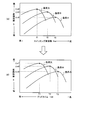
- FIG. 1 is a circuit diagram showing a configuration example of a DC-DC converter according to a first embodiment of the present invention. It is a block diagram which shows the structure of the control circuit in the said 1st Embodiment. 3 is a timing chart for explaining the operation of the DC-DC converter according to the first embodiment. It is a flowchart which shows the appropriate dead time search process performed with the control circuit in the said 1st Embodiment. It is a figure (A, B) for demonstrating the effect of the said 1st Embodiment, comparing with a prior art example.
- FIG. 5 is a circuit diagram showing another configuration example of the DC-DC converter according to the first embodiment.
- MOS Metal Oxide Semiconductor
- IGBT Insulated Gate Bipolar Transistors
- connection means “electrical connection” unless otherwise specified, and not only in the case of meaning direct connection within the scope of the present invention, but also through other elements. It also includes cases where it means indirect connection.
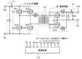
- FIG. 1 is a circuit diagram showing a configuration example of a phase shift DC-DC converter which is a power conversion apparatus according to the first embodiment of the present invention.
- This DC-DC converter includes a switch circuit 10 as an inverter, a rectifier circuit 20, a transformer T11, an input side measurement circuit 11, an output side measurement circuit 21, and a control circuit 110, and includes a high voltage side input terminal TiH. And a low voltage side input terminal TiL, a high voltage side output terminal ToH, and a low voltage side output terminal ToL.
- a DC input voltage Vin is applied between the high-voltage side input terminal TiH and the low-voltage side input terminal TiL, and a DC output voltage Vout whose level is converted is generated between the high-voltage side output terminal ToH and the low-voltage side output terminal ToL.
- the switch circuit 10 includes N-channel MOS transistors Q11 to Q14 as four switching elements, and these transistors Q11 to Q14 constitute a bridge circuit. That is, the first high-voltage transistor Q11 and the first low-voltage transistor Q12 are connected in series to form a first switching element pair, and the second high-voltage transistor Q13 and the second low-voltage transistor Q14 is connected in series with each other to form a second switching element pair, and the first switching element pair and the second switching element pair are connected in parallel with each other.
- the switch circuit 10 includes a coil L11. A connection point between the source terminal of the first high-voltage side transistor Q11 and the drain terminal of the first low-voltage side transistor Q12 is connected to the primary of the transformer T11 via the coil L11.
- a connection point between the source terminal of the second high voltage side transistor Q13 and the drain terminal of the second low voltage side transistor Q14 is connected to the other end of the primary side winding of the transformer T11.
- the drain terminals of the first and second high voltage side transistors Q11 and Q13 are both connected to the high voltage side input terminal TiH, and the source terminals of the first and second low voltage side transistors Q12 and Q14 are both connected to the low voltage side input terminal TiL.
- the coil L11 in the switch circuit 10 forms a resonance circuit with the source-drain capacitance which is the parasitic capacitance of the transistors Q11 to Q14, and the transistors Q11 to Q14 are switched by adjusting the phase of the current by the resonance phenomenon.
- the switching loss which is a power loss resulting from the crossing of the positive voltage waveform and the current waveform at a positive value, is reduced. That is, in the switch circuit 10, the switching loss is reduced by switching the transistors Q11 to Q14 in a state where the voltage or current is substantially zero (such switching is called “soft switching”).
- a resonance circuit may be configured using the leakage inductance of the primary side winding of the transformer T11.
- the position of the inductance as a constituent element of the resonance circuit is not limited to the position of the coil L11 or the leakage inductance, and may be in the path of the current flowing through each of the transistors Q11 to Q14.
- a capacitor is provided between both ends of each of the transistors Q11 to Q14 in the switch circuit 10, and this resonance circuit is configured using the capacitor instead of or in addition to the parasitic capacitance between the both ends. Good.
- the rectifier circuit 20 includes N-channel MOS transistors Q15 and Q16 as two switching elements with a built-in diode, a coil L12, and a capacitor C11.
- the transistor Q15 has a drain terminal connected to one end of the secondary winding of the transformer T11, and a source terminal connected to the low-voltage side output terminal ToL.
- the drain terminal of the transistor Q16 is connected to the other end of the secondary winding of the transformer T11, and the source terminal thereof is connected to the low voltage side output terminal ToL.
- the intermediate tap of the secondary winding of the transformer T11 is connected to the low-voltage side output terminal ToL via the coil L12 and the capacitor C11.
- the coil L12 and the capacitor C11 constitute an LC filter for smoothing, and the connection point between the coil 12 and the capacitor C11 is connected to the high-voltage side output terminal ToH.
- the cathode side terminal of the parasitic diode is the drain terminal
- the anode side terminal of the parasitic diode is the source terminal.
- the input voltage Vin is obtained on the input side in order to obtain the input power applied from the outside via the high-voltage side and low-voltage side input terminals TiH and TiL.
- An output side measurement circuit 21 for measuring the output current Iout is provided.
- a measured value of the input voltage Vin (hereinafter referred to as “input voltage measured value”) Vi and a measured value of the input current Iin (hereinafter referred to as “input current measured value”) Ii obtained by the input side measuring circuit 11 are input to the control circuit 110. Is done.
- the measured value of the output voltage Vout (hereinafter referred to as “output voltage measured value”) Vo and the measured value of the output current Iout (hereinafter referred to as “output current measured value”) Io obtained by the output side measuring circuit 21 are also input to the control circuit 110. Is done.
- the control circuit 110 receives the input voltage measurement value Vi, the input current measurement value Ii, the output voltage measurement value Vo, and the output current measurement value Io and receives the transistors Q11 to Q14 of the switch circuit 10 and the transistor Q15 of the rectifier circuit 20.
- Q16 are turned on / off, and switching control signals G1 to G16 are generated and applied to the gate terminals of the transistors Q11 to Q16, respectively.
- the switch circuit 10 operates as a phase shift inverter by the on / off operation of the transistors Q11 to Q14 based on the switching control signals G11 to G14, and rectifies by the on / off operation of the transistors Q15 and Q16 based on the switching control signals G15 and G16. In the circuit 20, conduction loss is suppressed.
- the switching frequency of the switch circuit 10 as an inverter that is, the switching frequency for turning on / off the transistors Q11 to Q14 is fixed.
- FIG. 2 is a block diagram showing a configuration of the control circuit 110 in the present embodiment.
- the control circuit 110 includes a feedback control calculation unit 111, a voltage command value setting unit 112, a switching control signal generation circuit 113, a drive circuit 114, a conversion efficiency calculation unit 116, and an appropriate dead time search control unit 118.
- the feedback control calculation unit 111, the conversion efficiency calculation unit 116, and the appropriate dead time search control unit 118 perform digital processing, and therefore are input to the control circuit 110 before these digital processing.
- the input voltage measurement value Vi, the input current measurement value Ii, the output voltage measurement value Vo, and the output current measurement value Io are converted into digital signals by an AD converter (not shown) (this point is different in other embodiments). The same).
- the feedback control calculation unit 111 performs a phase shift time Ts, which will be described later, by a control calculation based on the difference between the output voltage measured value Vo and the voltage command value Vref in order to maintain the output voltage Vout of the DC-DC converter at the voltage command value Vref.
- a phase shift time control signal Cts is generated.
- the phase shift time control signal Cts is input to the switching control signal generation circuit 113.
- the conversion efficiency calculation unit 116 calculates the conversion efficiency ⁇ of the DC-DC converter from the input voltage measurement value Vi, the input current measurement value Ii, the output voltage measurement value Vo, and the output current measurement value Io (hereinafter referred to as “this”).
- the conversion efficiency is also referred to as “calculated conversion efficiency ⁇ ”).
- the conversion efficiency calculation unit 116 determines whether or not the conversion efficiency ⁇ is smaller than a lower limit value (hereinafter referred to as “current lower limit value”) ⁇ clim determined according to the current load.
- a table that gives a relationship between the lower limit value ⁇ lim of the conversion efficiency and the output current Iout is held in advance in the conversion efficiency calculation unit 116, and the conversion efficiency calculation unit 116 refers to this table and outputs the measured output current value Io.
- This search necessity signal Csr is input to the appropriate dead time search control unit 118 together with the calculated conversion efficiency ⁇ .
- the search necessity signal Csr is input to the appropriate dead time search control unit 118 as a signal indicating “search required”.
- the appropriate dead time search control unit 118 executes an appropriate dead time search process, which will be described later, obtains an appropriate dead time Tdd, and outputs a dead time control signal Cdt indicating the appropriate dead time Tdd.
- the search necessity signal Csr is input to the appropriate dead time search control unit 118 as a signal indicating “no search required”. In this case, the appropriate dead time search control unit 118 outputs the current dead time control signal Cdt as it is without changing the later-described appropriate dead time search process.
- the switching control signal generation circuit 113 Based on the phase shift time control signal Cts from the feedback control calculation unit 111 and the dead time control signal Cdt from the appropriate dead time search control unit 118, the switching control signal generation circuit 113 performs transistors Q11 to Q11 of the switch circuit 10 according to the phase shift method. A control signal for turning on / off the transistors Q15 and Q16 of the Q14 and the rectifier circuit 20 is generated. The drive circuit 114 amplifies these control signals to a level capable of driving the transistors Q11 to Q16, and outputs them as switching control signals G11 to G16. These switching control signals G11 to G16 are applied to the gate terminals of the transistors Q11 to Q16.
- the control circuit 110 uses, for example, a microcomputer (hereinafter abbreviated as “microcomputer”) including a CPU (Central Processing Unit) and a memory, an AD converter and a DA converter, except for the drive circuit 114. By executing a program corresponding to the above-described operation, it can be realized by software. Alternatively, the control circuit 110 can be realized as dedicated hardware (typically, an application-specific integrated circuit designed exclusively). In this case, the feedback control calculation unit 111 and the conversion efficiency calculation unit 116 can be realized by combining a plurality of calculation units.
- the appropriate dead time search control unit 118 temporarily stores the current dead time TdA, the previous dead time TdB, the current conversion efficiency ⁇ A, and the previous conversion efficiency ⁇ B as can be understood from the description of the appropriate dead time search process (FIG. 4) described later. It can be realized in hardware by combining a register for holding data, several arithmetic units, a comparator, and the like.
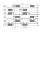
- FIG. 3 is a timing chart for explaining the operation of the DC-DC converter according to the present embodiment.
- the change in the on / off state of Q16 is shown.
- the ratio of the ON period of each of the transistors Q11 to Q14 in the switch circuit 10 to the switching cycle Tp, that is, the duty ratio is fixed.
- the output voltage Vout is controlled by changing the phase difference generated between the first switching element pair Q11 and Q12 and the second switching element pair Q13 and Q14.
- this phase difference is the period Ts in which the ON period of the first high-voltage side transistor Q11 and the ON period of the second low-voltage side transistor Q14 overlap, that is, the period Ts in which both the transistors Q11 and Q14 are in the ON state.
- Ts is referred to as “phase shift time Ts”).
- the feedback control calculation unit 111 determines the phase shift time control signal Cts. Calculation is performed (see FIG. 2).
- the transistors Q15 and Q16 are also controlled to be turned on / off in order to suppress conduction loss in the secondary side rectifier circuit 20 of the transformer T11 as much as possible. That is, the transistor Q15 is turned off in a period in which the dead times Td56 and Td57 are added before and after the period in which both the transistors Q11 and Q14 of the switch circuit 10 are turned on (a period corresponding to the phase shift time Ts). It is controlled by the switching control signal G15 so as to be in the on state in a period other than.
- the transistor Q16 is also turned off in a period in which the dead times Td56 and Td57 are added before and after the period in which both the transistors Q12 and Q13 of the switch circuit 10 are turned on (a period corresponding to the phase shift time Ts).
- the switching control signal G16 is controlled so as to be in an ON state during the period.
- a dead time Td12 in which both the transistors Q11 and Q12 constituting the first switching element pair are turned off and a dead time Td34 in which both the transistors Q13 and Q14 constituting the second switching element pair are turned off will be described later. 4 is determined by the appropriate dead time search process shown in the flowchart of FIG.
- the dead time provided immediately before the ON period of the first low-voltage side transistor Q12 and the dead time provided immediately after are set to the same time Td12. However, these dead times are different times. May be set.
- the dead time provided immediately before the ON period of the first high-voltage side transistor Q11 and the dead time provided immediately after it are set to the same time Td12, but these dead times are set to different times. Also good.
- the dead time provided immediately before the ON period of the second high-voltage side transistor Q13 and the dead time provided immediately after it are set to the same time Td34, but these dead times are set to different times. May be.
- the dead time Td12 provided before and after the on period of the first high voltage side transistor Q11 and the dead time Td34 provided before and after the on period of the second high voltage side transistor Q13 are the same time. Although set, the dead times Td12 and Td34 may be set to different times.
- FIG. 4 is a flowchart showing an appropriate dead time search process executed by the control circuit 110 in the present embodiment.
- the appropriate dead time search process is started and the appropriate dead time search control unit 118 operates as follows.
- the dead time Tdd corresponding to the dead times Td12 and Td34 shown in FIG. 3 is initialized (step S10). Specifically, a predetermined dead time initial value Td0 is substituted into the previous dead time TdB that is a variable introduced for searching for the appropriate dead time Tdd. In general, the optimum value of the dead time Tdd becomes shorter as the load increases (see FIG. 5 described later). For this reason, if a value longer than the expected optimum value of the dead time Tdd is set as the dead time initial value Td0, a large power loss occurs at a high load and a large amount of heat is generated in the circuit, so that reliability can be lowered. There is sex.
- the dead time initial value Td0 is set in advance to a value shorter than the expected optimum value of the dead time Tdd.
- the conversion efficiency ⁇ calculated by the conversion efficiency calculation unit 116 is a variable introduced to determine increase / decrease in conversion efficiency. Substitute into efficiency ⁇ B (step S12).
- the dead time control signal Cdt is input to the switching control signal generation circuit 113.
- the increment unit ⁇ T is selected so that the change in the conversion efficiency ⁇ is sufficiently small when the dead time Tdd is changed by the increment unit ⁇ T.
- the switch circuit 10 and the rectifier circuit 20 operate based on the dead time control signal Cdt, and the input voltage measured value Vi and the input current measured value Ii, the output voltage measured value Vo and the output current measured value Io obtained during the operation.
- step S20 the value of the current conversion efficiency ⁇ A is substituted for the previous conversion efficiency ⁇ B, and the value of the current dead time TdA is substituted for the previous dead time TdB. Thereafter, the process returns to step S14, and thereafter, while the current conversion efficiency ⁇ A is larger than the previous conversion efficiency ⁇ B, steps S14 to S20 are repeatedly executed. When the current conversion efficiency ⁇ A becomes equal to or lower than the previous conversion efficiency ⁇ B, the process proceeds to step S22. .
- the pre-conversion efficiency ⁇ B is substantially equal to the maximum conversion efficiency in the current load state. Accordingly, the dead time control signal Cdt indicating the previous dead time TdB is set to be output (step S22), and the appropriate dead time search process is terminated.
- switching control signals G11 to G16 generated by the switching control signal generation circuit 113 and the drive circuit 114 are applied to the gate terminals of the transistors Q11 to Q16.
- each step shown in FIG. 4 is executed by the microcomputer based on a predetermined program, and the processing of the conversion efficiency calculation unit 116 is also performed. It is executed by a microcomputer.
- FIG. 5A shows the change in conversion efficiency ⁇ when the load fluctuates in a conventional DC-DC converter with a fixed dead time
- FIG. 5B shows the DC- The change of conversion efficiency (eta) when the load fluctuates in the DC converter is shown.
- the dead time at which the conversion efficiency is maximized varies depending on the load as shown in FIG.
- Tdd the dead time at which the conversion efficiency is maximized
- the conversion efficiency is high when the load is large as shown in FIG. It decreases as ⁇ a1 ⁇ ⁇ b1 ⁇ ⁇ c1.
- the above-described appropriate dead time search process (FIG. 4) is executed.
- Time Tdd is set to T3.
- a dead time that maximizes the conversion efficiency is obtained by sequentially increasing the dead time Tdd from a value smaller than its expected optimum value (increment units ⁇ T).
- the optimum value of the dead time Tdd becomes shorter as the load is larger. Therefore, according to the appropriate dead time search process, conversion due to load fluctuation is avoided while avoiding a large power loss that causes heat generation that reduces reliability. The decrease in efficiency can be sufficiently suppressed.
- FIG. 6 is a circuit diagram showing another configuration example of the DC-DC converter according to the present embodiment.
- This DC-DC converter has the same configuration as the above-described configuration shown in FIG. 1 except for the configuration of the rectifier circuit 20. Therefore, hereinafter, the configuration of the rectifier circuit 20 in the other configuration example will be described, and the description of the configuration other than the rectifier circuit 20 will be omitted.
- the rectifier circuit 20 in the other configuration example includes MOS transistors Q17 and Q18 as two switching elements each including a diode, two coils L13 and L14, and a capacitor C12.
- the transistor Q17 has a drain terminal connected to one end of the secondary winding of the transformer T11, and a source terminal connected to the low-voltage side output terminal ToL.
- the drain terminal of the transistor Q18 is connected to the other end of the secondary side winding of the transformer T11, and the source terminal thereof is connected to the low voltage side output terminal ToL.
- the drain terminal of the transistor Q17 is connected to the high-voltage side output terminal ToH via the coil L13, and the drain terminal of the transistor Q18 is connected to the high-voltage side output terminal ToH via the coil L14.
- the capacitor C12 is connected between the high-voltage side output terminal ToH and the low-voltage side output terminal ToL, and the coils L13 and L14 constitute an LC filter for smoothing.
- the same signals as the switching control signals G15 and G16 generated by the control circuit 110 in the configuration example of FIG. 1 are generated as the switching control signals G17 and G18, respectively, and are applied to the gate terminals of the transistors Q17 and Q18. Each is given (see FIG. 6).
- switching control signals G11 to G14 are applied to the gate terminals of the transistors Q11 to Q14 in the switch circuit 10, respectively.
- the DC-DC converter according to the other configuration example of FIG. 6 operates in the same manner as the DC-DC converter according to the configuration example of FIG. 1 and has the same effect (see FIGS. 3 to 5).
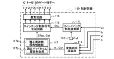
- FIG. 7 is a block diagram showing the configuration of the control circuit 120 in the DC-DC converter according to the present embodiment. Since the configuration of parts other than the control circuit 120 in this embodiment is the same as that of the first embodiment (see FIG. 1), the same parts are denoted by the same reference numerals, and the description thereof is omitted.
- control circuit 120 in the present embodiment also receives the input voltage measurement value Vi, the input current measurement value Ii, the output voltage measurement value Vo, and the output current measurement value Io.
- Switching control signals G1 to G16 for turning on / off the transistors Q11 to Q14 of the switch circuit 10 and the transistors Q15 and Q16 of the rectifier circuit 20 are generated and applied to the gate terminals of the transistors Q11 to Q16, respectively.
- the control circuit 120 is similar to the control circuit 110 (FIG. 2) in the first embodiment.
- the control circuit 120 in the present embodiment includes a search control unit 117 including an appropriate frequency search control unit 117a and an appropriate dead time search control unit 117b, instead of the appropriate dead time search control unit 118 in the first embodiment. ing.
- the search control unit 117 executes a proper dead time search process and a proper frequency search process, which will be described later, thereby obtaining an appropriate dead time TddP and an appropriate switching frequency fswP, and a dead time control signal Cdt and a switching indicating them, respectively.
- a frequency control signal Cfsw is generated.
- the dead time control signal Cdt and the switching frequency control signal Cfsw are input to the switching control signal generation circuit 113.
- the switching control signal generation circuit 113 is based on the phase shift time control signal Cts from the feedback control calculation unit 111, the dead time control signal Cdt and the switching frequency control signal Cfsw from the search control unit 117, and the transistor Q11 of the switch circuit 10.
- a control signal for turning on / off the transistors Q15 and Q16 of .about.Q14 and the rectifier circuit 20 is generated.
- control circuit 120 uses a microcomputer, an AD converter, and a DA converter except for the drive circuit 114, and the microcomputer executes a predetermined program. Therefore, it can be realized by software. Alternatively, the control circuit 120 can be realized as dedicated hardware.
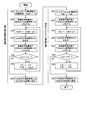
- FIG. 8 is a flowchart showing search processing executed by the control circuit 120 in the present embodiment.
- This search process includes an appropriate frequency search process executed by the appropriate frequency search control part 117a and an appropriate dead time search process executed by the appropriate dead time search control part 117b.
- the appropriate dead time search process (S50 to S62) is executed after the execution of the appropriate frequency search process (S30 to S42).
- a configuration in which search processing is executed may also be used.
- the search process is started when the search necessity signal Csr from the conversion efficiency calculation unit 116 indicates “search required”.
- the search control unit 117 is started. Works as follows.
- the switching frequency fsw is initialized (step S30). Specifically, a predetermined frequency initial value f0 is substituted into the previous switching frequency fswB that is a variable introduced for searching for an appropriate switching frequency. In general, the optimum value of the switching frequency fsw increases as the load increases (see FIG. 9A described later). For this reason, if a value lower than the predicted optimum value of the switching frequency fsw is set to the frequency initial value f0, the reliability may be reduced due to power loss caused by components as circuit components such as the transformer T11 at high load. There is.
- the frequency initial value f0 is set in advance to a value higher than the expected optimum value of the switching frequency fsw.
- the conversion efficiency ⁇ calculated by the conversion efficiency calculation unit 116 is a variable introduced to determine increase / decrease in conversion efficiency. Substitute into ⁇ B (step S32).
- the switching frequency control signal Cfsw is input to the switching control signal generation circuit 113.
- the decrement unit ⁇ f is selected so that the change in conversion efficiency ⁇ when the switching frequency fsw changes by this decrement unit ⁇ f is sufficiently small.
- the switch circuit 10 and the rectifier circuit 20 operate based on the switching frequency control signal Cfw, and the input voltage measurement value Vi and the input current measurement value Ii, the output voltage measurement value Vo and the output current measurement value Io obtained during the operation.
- step S40 the value of the current conversion efficiency ⁇ A is substituted for the previous conversion efficiency ⁇ B, and the value of the current switching frequency fswA is substituted for the previous switching frequency fswB. Thereafter, the process returns to step S34, and thereafter, while the current conversion efficiency ⁇ A is larger than the previous conversion efficiency ⁇ B, steps S34 to S40 are repeatedly executed. When the current conversion efficiency ⁇ A becomes equal to or lower than the previous conversion efficiency ⁇ B, the process proceeds to step S42. .
- step S42 the pre-conversion efficiency ⁇ B is almost equal to the maximum conversion efficiency when the switching frequency fsw is changed in the current load state. Therefore, the switching frequency control signal Cfsw indicating the previous switching frequency fsB is set to be output (step S42), the appropriate frequency search process is terminated, and the process proceeds to step S50.
- Step S50 When proceeding to step S50, the appropriate dead time search process is disclosed. Steps S50 to S62 constituting the appropriate dead time search process are the same as steps S10 to S22 constituting the appropriate dead time search process in the first embodiment (see FIG. 4), and thus description thereof is omitted. To do.
- the DC-DC converter At the time when the appropriate frequency search process (S30 to S42) is completed, the DC-DC converter is in a state of operating at a switching frequency at which the conversion efficiency ⁇ is substantially maximum when the switching frequency fsw is changed. .
- the DC-DC converter operates in a dead time in which the conversion efficiency ⁇ is substantially maximum when the dead time Tdd is changed. It has become. That is, at the time when the search process shown in FIG. 8 is completed, both the previous switching frequency fswB and the previous dead time TdB are almost optimal values, that is, appropriate values (hereinafter, these appropriate values are referred to as “fswP” and “TddP”). , Respectively).
- the search control unit 117 outputs the switching frequency control signal Cfsw and the dead time control signal Cdt indicating the appropriate switching frequency fswP and the dead time TddP, respectively, at the end of the search process (FIG. 8). (Steps S42 and S62). The outputs of the switching frequency control signal Cfsw and the dead time control signal Cdt are maintained until a search process is executed next and appropriate values of the switching frequency fsw and the dead time Tdd are newly calculated.
- transformer loss which represents a large proportion of DC-DC converter loss
- transformer loss is roughly divided into iron loss that occurs in the magnetic core, which is the path of magnetic flux, and copper loss that occurs due to the resistance component of the winding.
- the switching frequency of the DC-DC converter increases, the iron loss increases but the copper loss decreases.
- FIG. 9A there is a switching frequency at which the conversion efficiency of the DC-DC converter becomes maximum, that is, an optimum frequency, and this optimum switching frequency varies depending on the load.
- the above-described appropriate frequency search process (S30 to S42 in FIG. 9) is executed,
- the switching frequency fsw in the switch circuit 10 is automatically adjusted so that the conversion efficiency ⁇ is almost maximized at the load.
- fsw is set to f3.
- the appropriate dead time search process (S50 to S62 in FIG. 9) is executed in a state where the switching frequency fsw is set to the appropriate value fswP following the appropriate frequency search process.
- the dead time Tdd is adjusted so that the conversion efficiency ⁇ is substantially maximized.
- Tdd is set to T3.
- This DC-DC converter is configured to be able to supply two output voltages Vout1 and Vout2, and is used in, for example, a flat panel display device 131 as shown in FIG.
- a flat panel display 131 shown in FIG. 10 includes a PFC (Power Factor Correction) circuit 133, a DC-DC converter 134 according to the present embodiment, a control circuit including an image processing circuit, an audio processing circuit, and a panel driving circuit. 135, an antenna 139, an LED (Light Emitting Diode) drive circuit 136, and an LED backlight 137, and an AC voltage is supplied from an external AC power supply 132.
- a communication line 138 is provided between the DC-DC converter 134 and the control circuit 135 for exchanging information between them.
- the AC voltage from the AC power source is supplied to the PFC circuit 133, converted there to DC voltage, and then supplied to the DC-DC converter 134.
- the DC-DC converter 134 generates two direct current voltages having different levels from the direct current voltage and outputs them as output voltages Vout1 and Vout2.
- the output voltage Vout1 is supplied as a power supply voltage to the control circuit 135 including an image processing circuit, an audio processing circuit, and a panel drive circuit
- the output voltage Vout2 is supplied to the LED drive circuit 136 as a power supply voltage.
- the control circuit 135 of the flat panel display 131 includes an interface circuit for transmitting / receiving signals to / from an external device and a radio wave received by the antenna 139 in addition to the image processing circuit, the sound processing circuit, and the panel driving circuit. Also included are a decoding circuit for decoding the signal into a digital signal, a decoding / encoding circuit for transmitting / receiving information connected to the Internet, a power supply circuit for supplying an appropriate voltage to each of the above circuits, and the like. However, since these are not directly related to the present invention, description thereof is omitted.
- the voltage related to the DC-DC converter 134 will be specifically described.
- an AC voltage of 100 V is input from the AC power source 132 to the PFC circuit 133, and a DC voltage of 400 V is output from the PFC circuit 133, thereby the DC-DC converter. It is input to 134.
- a DC voltage of 12V and 90V is generated from the DC-DC converter 134.
- the DC voltage of 12V is supplied to the control circuit 135, and the DC voltage of 90V is supplied to the LED drive circuit 136.
- the configuration illustrated in FIG. 10 is merely an example, and for example, a configuration in which a DC voltage is directly supplied from the DC-DC converter 134 to the LED backlight 137 without providing the LED drive circuit 136 may be employed. .
- FIG. 11 is a circuit diagram showing a configuration of a phase shift DC-DC converter according to the present embodiment.
- This DC-DC converter includes a switch circuit 30 as an inverter, two rectifier circuits 41 and 42, a transformer T21, an input side measurement circuit 31, two output side measurement circuits 45 and 46, and a control circuit 210. And has a high voltage side input terminal TiH and a low voltage side input terminal TiL, two high voltage side output terminals ToH1, ToH2, and two low voltage side output terminals ToL1, ToL2.
- a direct-current input voltage Vin is applied between the high-voltage side input terminal TiH and the low-voltage side input terminal TiL, and a level-converted direct-current voltage is applied between the first high-voltage side output terminal ToH1 and the first low-voltage side output terminal ToL1.
- the first output voltage Vout1 is generated, and the second output voltage Vout2 that is a DC voltage whose level is converted between the second high-voltage side output terminal ToH2 and the second low-voltage side output terminal ToL2 is generated. Is generated (Vout1 ⁇ Vout2).
- this DC-DC converter includes two rectifier circuits 41, 42, two output side measurement circuits 45, 46 corresponding to them, and two pairs of output terminals ToH1, ToL1, ToH2, ToL2.
- the transformer T21 and the control circuit 210 are configured according to these differences.
- other configurations in the present embodiment are the same as those in the first embodiment, and the configurations of the rectifier circuits 41 and 42 and the output side measurement circuits 45 and 46 are the same as those in the first embodiment. Since it is the same as that of the rectifier circuit 20 and the output side measurement circuit 21, detailed description of the configuration of the present embodiment other than the control circuit 210 will be omitted.
- the transistors Q11 to Q14 in the first embodiment correspond to the transistors Q21 to Q24 in the present embodiment, respectively, and the transistors Q15 and Q16, the coil L12, and the capacitor C11 in the first embodiment are the same as those in the present embodiment.
- the transistors correspond to the transistors Q25 and Q26, the coil L22, and the capacitor C21, respectively, and correspond to the transistors Q27 and Q28, the coil L23, and the capacitor C22 in the present embodiment, respectively.
- FIG. 12 is a block diagram showing the configuration of the control circuit 210 in the DC-DC converter according to the present embodiment.
- the same or corresponding parts as those of the control circuit 110 in the first embodiment are denoted by the same reference numerals, and detailed description thereof is omitted.
- a first output voltage measured value Vo1 that is a measured value of the first output voltage Vout1 obtained by the first output side measuring circuit 45 is input to the feedback control calculation unit 111.
- the feedback control calculation unit 111 sets the phase shift time Ts by a control calculation based on the difference between the first output voltage measurement value Vo1 and the voltage command value Vref so as to maintain the first output voltage Vout1 at the voltage command value Vref.
- the phase shift time control signal Cts shown is generated.
- the phase shift time control signal Cts is input to the switching control signal generation circuit 113.
- the conversion efficiency calculation unit 116 in the control circuit 210 includes an input voltage measurement value Vi and an input current measurement value Ii obtained by the input side measurement circuit 31, and a first output voltage measurement value Vo1 obtained by the first output side measurement circuit 45.
- the first output current measurement value Io1, the second output voltage measurement value Vo2 and the second output current measurement value Io2 obtained by the second output side measurement circuit 46 are input.
- the conversion efficiency calculation unit 116 includes the input voltage measurement value Vi, the input current measurement value Ii, the first output voltage measurement value Vo1, the first output current measurement value Io1, the second output voltage measurement value Vo2, and the second
- the conversion efficiency ⁇ of this DC-DC converter is calculated from the measured output current value Io2.
- Other functions and operations of the conversion efficiency calculation unit 116 are the same as those of the conversion efficiency calculation unit 116 in the first embodiment.
- the appropriate dead time search control unit 118 operates in the same manner as the appropriate dead time search control unit 118 in the first embodiment and has the same function (see FIG. 4), and also displays a flat panel display via the communication line 138.
- Information is exchanged with the control circuit 135 of the device 131 (FIG. 10).
- the appropriate dead time search control unit 118 obtains information indicating the processing amount in the flat panel display 131, for example, an approximate value of the load based on image information to be processed, from the control circuit 135 in advance to the communication line 138.
- the dead time initial value Td0 of the appropriate dead time search process can be determined based on this approximate value. As a result, the time from the start to the end of the appropriate dead time search process is greatly reduced.
- the appropriate dead time search control unit 118 detects the occurrence of an abnormality from a large decrease in the conversion efficiency ⁇ calculated by the conversion efficiency calculation unit 116 and sends warning information indicating the occurrence of the abnormality via the communication line 138 to the control circuit 135. Can be sent to. As a result, the control circuit 135 stops the operation of the entire flat panel display device based on the warning information, thereby preventing a major accident due to a failure.
- the switching control signal generation circuit 113 and the driving circuit 114 operate in the same manner as the switching control signal generation circuit 113 and the driving circuit 114 in the first embodiment, and have the same functions, but the switching control signal in the first embodiment.
- switching control signals G21 to G26 corresponding to G11 to G16 switching control signals G27 and G28 are generated.
- the switching control signals G27 and G28 are the same signals as the switching control signals G25 and G26, respectively.
- FIG. 13 is a timing chart for explaining the operation of the DC-DC converter according to the present embodiment.
- the change in the on / off state of Q28 is shown.
- the phase shift method is also adopted in the present embodiment, and as can be seen from the comparison with the timing chart of FIG. 3 in the first embodiment, the transistor Q21 in the present embodiment and the transistor Q11 in the first embodiment described above. Are operated by the same switching control signal (G21, G11).
- the transistor Q22 and the transistor Q12 operate with the same switching control signal (G22, G12)
- the transistor Q23 and the transistor Q13 operate with the same switching control signal (G23, G13)
- the transistor Q24 and the transistor Q14 are operated by the same switching control signal (G24, G14)
- the transistors Q25 and Q27 and the transistor Q15 are operated by the same switching control signal (G25, G27, G15)
- the transistors Q26 and Q28 and the transistor Q16 are It operates by the same switching control signal (G26, G28, G16).
- the deadline is obtained by exchanging information between the control circuit 210 (the appropriate dead time search control unit 118) of the DC-DC converter and the control circuit 135 of the flat panel display device by the communication line 138.
- the time for searching for an appropriate dead time is greatly shortened, or warning information for occurrence of abnormality is sent to the control circuit 135 of the flat panel display device based on a large decrease in conversion efficiency ⁇ . You can also.
- each of the rectifier circuits 41 and 42 has the same configuration as the rectifier circuit 20 in the configuration example shown in FIG. 1 for the first embodiment. Instead, it may have the same configuration as the rectifier circuit 20 in the other configuration example shown in FIG.
- phase shift type DC-DC converter As an example, and the phase shift method is effective in suppressing switching loss.
- the present invention is not limited to this, as long as it is a power conversion circuit including a bridge circuit having a switching element pair including a high-voltage side switching element constituting an upper arm and a low-voltage side switching element constituting a lower arm. Applicable.
- control circuits 110, 120, and 210 in each of the above embodiments are not limited to the configurations shown in FIGS. 2, 4, 7, 8, and 12, and a decrease in conversion efficiency due to load fluctuation is suppressed. As long as one or both of the dead time Tdd and the switching frequency fsw are automatically adjusted, any configuration may be used.
- the control circuits 110, 120, and 210 may be realized by dedicated hardware (typically, an application-specific integrated circuit designed exclusively), or a part or all of the main part thereof may be realized by software. It may be realized.
- Each of the input side measurement circuits 11, 31 and the output side measurement circuits 21, 45, 46 in each of the above embodiments is configured to measure both voltage and current in order to obtain input power and output power.
- the conversion efficiency calculation unit 116 of the control circuit calculates the conversion efficiency ⁇ using both the measured values of voltage and current.
- the input power or the output power is calculated using only the corresponding current measurement value, and the calculation result is Alternatively, the conversion efficiency ⁇ may be calculated.
- the lower limit value ⁇ lim of the conversion efficiency it is preferable to set the lower limit value ⁇ lim of the conversion efficiency so that the appropriate dead time search process and / or the appropriate frequency search process is started only when the conversion efficiency is greatly lowered due to the load fluctuation.
- the present invention is not limited to this.
- the lower limit value ⁇ lim of the conversion efficiency may be set so that an appropriate dead time search process or the like is started when the decrease in conversion efficiency is relatively small.
- the present invention can be applied to a power conversion device such as a DC-DC converter including a bridge circuit configured using a plurality of switching elements and a control method thereof.
- Switch circuit (inverter) DESCRIPTION OF SYMBOLS 11, 31 ... Input side measuring circuit 21, 45, 46 ... Output side measuring circuit 20 ... Rectifier circuit 38 ... Communication line 110, 120, 210 ... Control circuit (control part) 113 ... Switching control signal generation circuit (control signal generation unit) 116: Conversion efficiency calculation unit 117 ... Search control unit 117a ... Appropriate frequency search control unit 117b ... Appropriate dead time search control unit 118 ... Appropriate dead time search control unit 134 ... DC-DC converters T11, T21 ... Transformer TiH ...
- High voltage side Input terminal TiL Low voltage side input terminals ToH, ToH1, ToH2: High voltage side output terminals ToL, ToL1, ToL2: Low voltage side output terminals Q11 to Q18 ... Transistors (switching elements) Q21 to Q28 ... Transistor (switching element) G11 to G18 ... switching control signals G21 to G28 ... switching control signal Cts ... phase shift time control signal Cdt ... dead time control signal Cfsw ... switching frequency control signal Vi ... input voltage measurement value Ii ... input current measurement values Vo, Vo1, Vo2 ... Output voltage measurement values Io, Io1, Io2 ... Output current measurement value Ts ... Phase shift time Tp ... Switching cycle
Landscapes
- Engineering & Computer Science (AREA)
- Power Engineering (AREA)
- Dc-Dc Converters (AREA)
Abstract
La présente invention concerne un dispositif de conversion de puissance qui peut suffisamment empêcher une diminution du rendement de conversion due à des fluctuations de charge même si les caractéristiques d'un élément de circuit varient ou changent. Si le rendement de conversion η chute en raison de fluctuations de charge dans un convertisseur continu-continu, une valeur inférieure à une valeur optimale anticipée de temps mort Tdd dans un état post-fluctuation de charge est utilisée comme valeur initiale pour calculer le rendement de conversion η par des opérations dans lesquelles le temps mort Tdd est augmenté séquentiellement par unités d'incrément prédéterminé ΔT. Grâce à cette configuration, un temps mort approprié TddP est trouvé dans lequel le rendement de conversion η est sensiblement maximisé dans l'état post-fluctuation de charge, et un élément de commutation est commandé de manière à exécuter un déblocage et un blocage au niveau de ce temps mort approprié TddP.
Applications Claiming Priority (2)
| Application Number | Priority Date | Filing Date | Title |
|---|---|---|---|
| JP2015139652 | 2015-07-13 | ||
| JP2015-139652 | 2015-07-13 |
Publications (1)
| Publication Number | Publication Date |
|---|---|
| WO2017010134A1 true WO2017010134A1 (fr) | 2017-01-19 |
Family
ID=57757919
Family Applications (1)
| Application Number | Title | Priority Date | Filing Date |
|---|---|---|---|
| PCT/JP2016/061990 Ceased WO2017010134A1 (fr) | 2015-07-13 | 2016-04-14 | Dispositif de conversion de puissance et son procédé de commande |
Country Status (1)
| Country | Link |
|---|---|
| WO (1) | WO2017010134A1 (fr) |
Cited By (2)
| Publication number | Priority date | Publication date | Assignee | Title |
|---|---|---|---|---|
| EP3582384A4 (fr) * | 2017-02-07 | 2020-02-19 | Mitsubishi Electric Corporation | Dispositif de conversion de puissance |
| EP3806306A1 (fr) * | 2019-10-11 | 2021-04-14 | Deere & Company | Procédé et système de commande d'un convertisseur de courant continu en courant continu |
Citations (3)
| Publication number | Priority date | Publication date | Assignee | Title |
|---|---|---|---|---|
| US20050281058A1 (en) * | 2004-06-21 | 2005-12-22 | Issa Batarseh | Dynamic optimization of efficiency using dead time and FET drive control |
| JP2010193684A (ja) * | 2009-02-20 | 2010-09-02 | Oki Power Tech Co Ltd | 電源装置 |
| WO2015079573A1 (fr) * | 2013-11-29 | 2015-06-04 | 新電元工業株式会社 | Dispositif d'alimentation électrique, dispositif d'inspection, et procédé d'optimisation pour dispositif d'alimentation électrique |
-
2016
- 2016-04-14 WO PCT/JP2016/061990 patent/WO2017010134A1/fr not_active Ceased
Patent Citations (3)
| Publication number | Priority date | Publication date | Assignee | Title |
|---|---|---|---|---|
| US20050281058A1 (en) * | 2004-06-21 | 2005-12-22 | Issa Batarseh | Dynamic optimization of efficiency using dead time and FET drive control |
| JP2010193684A (ja) * | 2009-02-20 | 2010-09-02 | Oki Power Tech Co Ltd | 電源装置 |
| WO2015079573A1 (fr) * | 2013-11-29 | 2015-06-04 | 新電元工業株式会社 | Dispositif d'alimentation électrique, dispositif d'inspection, et procédé d'optimisation pour dispositif d'alimentation électrique |
Cited By (2)
| Publication number | Priority date | Publication date | Assignee | Title |
|---|---|---|---|---|
| EP3582384A4 (fr) * | 2017-02-07 | 2020-02-19 | Mitsubishi Electric Corporation | Dispositif de conversion de puissance |
| EP3806306A1 (fr) * | 2019-10-11 | 2021-04-14 | Deere & Company | Procédé et système de commande d'un convertisseur de courant continu en courant continu |
Similar Documents
| Publication | Publication Date | Title |
|---|---|---|
| US7944715B2 (en) | Controller for use in a resonant direct current/direct current converter | |
| US20180062529A1 (en) | Converter and control method thereof | |
| US9343986B2 (en) | Power converter with current feedback loop | |
| JP5807658B2 (ja) | 電力変換装置及び電力変換方法 | |
| JP7124297B2 (ja) | 電力変換装置 | |
| WO2018216294A1 (fr) | Convertisseur cc/cc | |
| US11539299B2 (en) | Switching power supply unit and electric power supply system | |
| JP5838997B2 (ja) | 電力変換装置及び電力補正方法 | |
| JP5807659B2 (ja) | 電力変換装置及び電力変換方法 | |
| US10622905B2 (en) | DC-DC converter | |
| CN104067498A (zh) | 以最大化功率效率来控制开关模式电源 | |
| US9641062B2 (en) | Switching power supply, method for controlling switching power supply, and power supply system | |
| JP6684637B2 (ja) | 共振形電源装置 | |
| JP2014017960A (ja) | スイッチング電源装置 | |
| WO2015079573A1 (fr) | Dispositif d'alimentation électrique, dispositif d'inspection, et procédé d'optimisation pour dispositif d'alimentation électrique | |
| WO2017149906A1 (fr) | Circuit d'alimentation à découpage | |
| JP2013172467A (ja) | スイッチング電源回路 | |
| JP6358861B2 (ja) | 絶縁抵抗測定装置 | |
| JP6015947B2 (ja) | スイッチング電源装置、及びその制御方法 | |
| US20070063679A1 (en) | Multi-phase buck converter | |
| JP2011188708A (ja) | スイッチング電源 | |
| JP5642625B2 (ja) | スイッチング電源装置 | |
| JP6662151B2 (ja) | Dc/dc変換装置、コンピュータプログラム及びdc/dc変換装置の制御方法 | |
| TWI772215B (zh) | 應用於返馳式電源轉換器的控制器的效率追蹤方法 | |
| JP2014197949A (ja) | 電力変換回路 |
Legal Events
| Date | Code | Title | Description |
|---|---|---|---|
| 121 | Ep: the epo has been informed by wipo that ep was designated in this application |
Ref document number: 16824115 Country of ref document: EP Kind code of ref document: A1 |
|
| NENP | Non-entry into the national phase |
Ref country code: DE |
|
| NENP | Non-entry into the national phase |
Ref country code: JP |
|
| 122 | Ep: pct application non-entry in european phase |
Ref document number: 16824115 Country of ref document: EP Kind code of ref document: A1 |