WO2017010177A1 - Capteur - Google Patents
Capteur Download PDFInfo
- Publication number
- WO2017010177A1 WO2017010177A1 PCT/JP2016/065773 JP2016065773W WO2017010177A1 WO 2017010177 A1 WO2017010177 A1 WO 2017010177A1 JP 2016065773 W JP2016065773 W JP 2016065773W WO 2017010177 A1 WO2017010177 A1 WO 2017010177A1
- Authority
- WO
- WIPO (PCT)
- Prior art keywords
- sensor
- oscillator
- resonators
- inspected
- state
- Prior art date
- Legal status (The legal status is an assumption and is not a legal conclusion. Google has not performed a legal analysis and makes no representation as to the accuracy of the status listed.)
- Ceased
Links
Images


Classifications
-
- G—PHYSICS
- G01—MEASURING; TESTING
- G01N—INVESTIGATING OR ANALYSING MATERIALS BY DETERMINING THEIR CHEMICAL OR PHYSICAL PROPERTIES
- G01N22/00—Investigating or analysing materials by the use of microwaves or radio waves, i.e. electromagnetic waves with a wavelength of one millimetre or more
-
- G—PHYSICS
- G01—MEASURING; TESTING
- G01N—INVESTIGATING OR ANALYSING MATERIALS BY DETERMINING THEIR CHEMICAL OR PHYSICAL PROPERTIES
- G01N27/00—Investigating or analysing materials by the use of electric, electrochemical, or magnetic means
- G01N27/02—Investigating or analysing materials by the use of electric, electrochemical, or magnetic means by investigating impedance
-
- G—PHYSICS
- G01—MEASURING; TESTING
- G01N—INVESTIGATING OR ANALYSING MATERIALS BY DETERMINING THEIR CHEMICAL OR PHYSICAL PROPERTIES
- G01N27/00—Investigating or analysing materials by the use of electric, electrochemical, or magnetic means
- G01N27/72—Investigating or analysing materials by the use of electric, electrochemical, or magnetic means by investigating magnetic variables
-
- G—PHYSICS
- G01—MEASURING; TESTING
- G01R—MEASURING ELECTRIC VARIABLES; MEASURING MAGNETIC VARIABLES
- G01R27/00—Arrangements for measuring resistance, reactance, impedance, or electric characteristics derived therefrom
- G01R27/02—Measuring real or complex resistance, reactance, impedance, or other two-pole characteristics derived therefrom, e.g. time constant
- G01R27/26—Measuring inductance or capacitance; Measuring quality factor, e.g. by using the resonance method; Measuring loss factor; Measuring dielectric constants ; Measuring impedance or related variables
Definitions
- the present invention relates to a sensor device.
- a sensor IC formed of a semiconductor integrated circuit may be able to satisfy such required performance.
- Patent Document 1 discloses a measurement system that detects the amount and movement of magnetic particles in a sample.
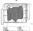
- FIG. 16 is a diagram for explaining the sensor IC described in Patent Document 1.
- FIG. FIG. 16A is a circuit diagram illustrating a schematic configuration of the oscillator 110 and the oscillator 120 included in the sensor IC described in Patent Document 1.
- FIG. FIG. 16B is a perspective view showing a schematic configuration of the sensor IC described in Patent Document 1.
- FIG. FIG. 16C is a perspective view showing a state in which the device under test 114 is attached to the sensor IC described in Patent Document 1.
- FIG. FIG. 16D is a perspective view showing a state in which the inspection object 114 and the inspection object 124 serving as a reference are attached to the sensor IC described in Patent Document 1.
- FIG. 17 is a diagram for explaining the oscillator 110 included in the sensor IC described in Patent Document 1.
- FIG. 17A is a partial view of FIG. 16A
- FIG. 17B is a BB ′ cross-sectional view.
- the sensor IC described in Patent Document 1 includes an oscillator 110 having an inductor 111 and an oscillator 120 having an inductor 121.
- the oscillator 110 and the oscillator 120 are selectively driven by a control signal (enable or non-enable).
- a control signal enable or non-enable
- the oscillator 110 and the oscillator 120 are mounted on the semiconductor substrate 101, for example, as shown in FIG.
- FIG. 16B the part other than the inductor 111 of the oscillator 110 is shown as the other circuit 112
- the part other than the inductor 121 of the oscillator 120 is shown as the other circuit 122.
- the oscillation frequency at which the oscillator 110 oscillates due to the magnetic permeability of the magnetic particles 113 Changes. From the difference between the oscillation frequency of the reference oscillator 120 and the changed oscillation frequency of the oscillator 110, it can be detected that the magnetic particles 113 are present in the vicinity of the oscillator 110. From the presence of the magnetic particles 113, it is estimated that the test object 114 labeled with the magnetic particles 113 is present in the vicinity of the oscillator 110. In addition, as shown in FIG. 16 (d), the characteristics of the oscillation frequency response of the oscillator 110 and the oscillator 120 can be examined by using a test object 124 that is not labeled with magnetic particles.
- the inductor 111 is formed in a metal layer (metal layer). Therefore, as shown in FIG. 17B, even if the inductor 111 is formed on the uppermost metal layer 130 of the semiconductor substrate 101, an insulator or the like is provided between the surface of the semiconductor substrate 101 and the inductor 111. There is a protective film 115 formed in (1). For this reason, the device under test 114 does not directly contact the inductor 111. Similarly, the inductor 121 is also formed in the metal layer. For this reason, the device under test 124 does not directly contact the inductor 121.
- FIG. 18 shows a case where the device under test 140 adheres to a wider area than the oscillator 110 and the oscillator 120, and a case where a portion 141 and a portion 142 having different physical properties exist inside the device under test 140. .
- the oscillator 110 and the oscillator 120 cannot individually measure the physical property at the portion 141 and the physical property at the portion 142.
- the present invention has been made in view of the above problems, and its purpose is to increase the spatial resolution for detecting the distribution of physical properties of the object to be inspected over a wide range. It is also an object of the present invention to detect local changes in physical properties of the object to be inspected by increasing the spatial resolution.
- a sensor device includes a substrate and a plurality of resonators disposed on the substrate, and each of the plurality of resonators is in the vicinity of itself.
- the resonance frequency is changed according to the physical property of the object to be inspected, and the distribution of the physical property of the object to be inspected is detected based on the distribution of the plurality of resonators and the resonance frequency of each of the plurality of resonators.
- the center distance between two resonators adjacent to each other among the plurality of resonators is 300 ⁇ m or less.
- the resonator is not a narrowly-defined antenna that transmits and receives electromagnetic waves, and is not restricted by the aperture diameter depending on the wavelength, so that the area can be reduced.
- substrate can be raised by the area reduction of a resonator. Therefore, it is possible to detect the distribution of physical properties of the object to be inspected in a wide range and increase the spatial resolution. And since it is not restricted by the wavelength, it is possible to detect local changes in the physical properties of the object to be inspected with a high spatial resolution that cannot be realized when narrowly defined antennas are arranged in an array.
- the object to be inspected need not be labeled with magnetic particles or the like. For this reason, the measurement work can be simplified.
- the arrangement density of the resonators can be increased. For this reason, the sensor device can be miniaturized. Alternatively, the spatial resolution of the sensor device can be increased.
- FIG. 2A is a circuit diagram showing a schematic configuration of the oscillator.
- FIG. 2B is a cross-sectional view taken along the line AA ′ showing a schematic configuration of the oscillator. It is a figure which shows the 2nd state to which the to-be-inspected object has adhered to the surface of sensor IC contained in the sensor apparatus shown in FIG. It is a figure for demonstrating the oscillation frequency of an oscillator in the sensor apparatus shown in FIG.
- FIG. 4A is a diagram showing the oscillation frequency of the first state oscillator
- FIG. 4B is a diagram showing the oscillation frequency of the second state oscillator with respect to the first state.
- It is a circuit diagram which shows another schematic structure of the oscillator contained in the sensor apparatus shown in FIG.
- It is a circuit diagram which shows another schematic structure of the oscillator contained in the sensor apparatus shown in FIG.
- It is a figure which shows the 3rd state to which the to-be-inspected object has adhered to the surface of sensor IC of the sensor apparatus shown in FIG.
- FIG. 3 is a diagram illustrating an oscillation frequency of an oscillator in a third state with respect to a second state in the sensor device illustrated in FIG. 1.
- FIG. 6 is a diagram illustrating an oscillation frequency of an oscillator in a fourth state with respect to a second state in the sensor device illustrated in FIG. 1.
- FIG. 2 is a schematic diagram for explaining control for sequentially driving unit cells A11 to ALM included in the sensor device 100 shown in FIG.
- FIG. 2 is a schematic diagram for explaining control for sequentially driving unit cells A11 to ALM included in the sensor device 100 shown in FIG.
- FIG. 2 is a perspective view which shows schematic structure of another sensor IC contained in the sensor apparatus 100 shown in FIG. 1, and is a figure which shows the 1st state where the surface of sensor IC is clean.
- FIG. 16A is a circuit diagram illustrating a schematic configuration of a plurality of oscillators included in the sensor IC described in Patent Document 1.
- FIG. 16B is a perspective view showing a schematic configuration of the sensor IC described in Patent Document 1.
- FIG. 16C is a perspective view showing a state in which an object to be inspected is attached to the sensor IC described in Patent Document 1.
- FIG. FIG. 16D is a perspective view showing a state in which the object to be inspected and the reference object to be inspected are attached to the sensor IC described in Patent Document 1.
- 6 is a diagram for explaining an oscillator included in a sensor IC described in Patent Document 1.
- FIG. 17A is a perspective view partially showing FIG. 16A
- FIG. 17B is a cross-sectional view along BB ′. It is a figure explaining the problem of the sensor IC described in Patent Document 1.
- the object to be inspected adheres to a wider range than the plurality of oscillators, and there are a plurality of parts having different physical properties inside the object to be inspected If you want to:
- Embodiment 1 Embodiment 1 of the present invention will be described below with reference to FIGS.
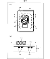
- FIG. 1 is a perspective view showing a schematic configuration of a sensor device 100 according to the present invention, and shows a first state in which the surface of a sensor IC 1 of the sensor device 100 is clean.
- the sensor device 100 includes a sensor IC 1, a detection circuit 3, and a control circuit 4.
- the sensor IC 1 is an integrated circuit for sensors (IntegratedirCircuit).
- the sensor IC1 includes a semiconductor substrate 10 and a plurality of unit cells A11 to ALM.
- Each of the unit cells A11 to ALM is a circuit formed on the semiconductor substrate 10.
- the plurality of unit cells A11 to ALM are arranged in a matrix form having L rows and M columns and having a row interval and a column interval of 300 ⁇ m or less.
- Each of unit cells A11 to ALM has the same configuration and includes an oscillator 20 and a frequency divider 30, respectively.
- the frequency divider 30 is a frequency divider that divides the oscillation frequency oscillated by the oscillator 20, and is provided in a one-to-one correspondence with the oscillator 20.
- the frequency dividing ratio of the frequency divider 30 is 1 / N (N is a rational number of 1 or more).
- the frequency divider 30 sets the frequency of the signal input to the detection circuit 3 to 1 / N times the oscillation frequency of the oscillator 20 so that the detection circuit 3 can easily handle the signal input to the detection circuit 3. As a result, the frequency of the signal input to the detection circuit 3 falls within the frequency band in which the detection circuit 3 operates.
- the control circuit 4 is a circuit that outputs a control signal (enable or non-enable) for selectively driving the plurality of unit cells A11 to ALM, and the driving unit cell is a plurality of unit cells A11 to ALM. It is grasped which is.
- the detection circuit 3 calculates the oscillation frequency of the oscillator 20 by adding the reciprocal number N of the frequency division ratio of the frequency divider 30 to the frequency of the signal output from the unit cell being driven.
- the control circuit 4 and the detection circuit 3 may be formed on the semiconductor substrate 10 or may be formed on a member different from the semiconductor substrate 10.
- FIG. 2 is a diagram for explaining a schematic configuration of the oscillator 20 included in the sensor device 100 shown in FIG.
- FIG. 2A is a circuit diagram showing a schematic configuration of the oscillator 20.
- FIG. 2B is an AA ′ cross-sectional view showing a schematic configuration of the oscillator 20.
- the oscillator 20 includes a differential circuit 40, a resonator 50 formed between the differential circuits 40, and a current source 60 that controls driving of the oscillator 20 according to a control signal.
- the oscillation frequency that the oscillator 20 oscillates is 30 GHz or more and 200 GHz or less.
- the differential circuit 40 includes an NMOS transistor M1 and an NMOS transistor M2 that are cross-coupled to each other. Note that another differential circuit may be used as appropriate. For example, a bipolar transistor may be used.
- the resonator 50 includes an inductor 52 and a capacitor 54 connected in parallel between the differentials of the differential circuit 40.
- the resonance frequency at which the resonator 50 resonates is the oscillation frequency at which the oscillator 20 oscillates. Since the resonator 50 is not a narrowly defined antenna that transmits and receives electromagnetic waves, the resonator 50 is not limited by the aperture diameter due to the wavelength. For this reason, the size of the resonator 50 can be set to 200 ⁇ m square or less (a size that fits in a square having a side of 200 ⁇ m), which is smaller than a quarter wavelength of a wavelength of about 1.5 mm of an electromagnetic wave of 200 GHz.
- the inductor 52 is formed in the uppermost layer (the layer closest to the contact position between the substrate and the object to be inspected) among the metal layers of the semiconductor substrate 10.
- the inductor 52 occupies most of the circuit size of the resonator 50.
- the resonator 50 occupies most of the circuit size of the oscillator 20.
- the area of the inductor 52 is determined so that the size of the resonator 50 in a plan view is a size that fits in a square having a side of 200 ⁇ m.
- the capacitor 54 may be formed by gate capacitances of the transistors M1 and M2, parasitic capacitances of wirings not shown, and the like.
- the inductor 52 is covered with a protective film 15 formed of an insulator or the like. For this reason, moisture, an object to be inspected, and the like do not directly contact the inductor 52. Since the inductor 52 is formed in the metal layer that is the uppermost layer, the resonance frequency of the resonator 20 changes due to the water molecules near the surface of the semiconductor substrate 10 and the water state related to the object to be inspected. To do. More specifically, the dielectric constant around the metal layer, which is the uppermost layer, changes due to changes in the state of water associated with water molecules and the object to be inspected. As a result, the parasitic capacitance value that affects the resonator 20 changes.
- At least one of the inductor 52 and the capacitor 54 includes a metal layer that is the uppermost layer, and a capacitance that affects the one. It only has to change the value.
- the inductor 52 and the capacitor 54 form an LC circuit, and the resonance frequency of the resonator 50 and the oscillation frequency of the oscillator 20 are determined by the inductance of the inductor 52 and the capacitance of the capacitor 54. For example, when the inductance of the inductor 52 is around 1 nH and the capacitance of the capacitor 54 is around 27 fF, the resonance frequency of the resonator 50 and the oscillation frequency of the oscillator 20 are around 30 GHz.
- FIG. 3 is a diagram showing a second state in which the device under test 70 is attached to the surface of the sensor IC 1 included in the sensor device 100 shown in FIG.
- the test object 70 is a sample containing moisture, and examples thereof include various types of cells, proteins, inorganic aqueous solutions, and organic aqueous solutions.
- the control circuit 4 selectively drives and drives the plurality of unit cells A11 to ALM with the surface of the sensor IC 1 clean (first state) as shown in FIG.
- the detection circuit 3 measures the frequency of the signal output from the unit cell. Then, the detection circuit 3 calculates the oscillation frequency of the oscillator 20 by accumulating the reciprocal number N of the frequency division ratio of the frequency divider 30 to the frequency of the measured signal.
- the object 70 is adhered to the surface of the sensor IC1. Then, as shown in FIG. 3, the dielectric constant of the surface of the semiconductor substrate 10 changes due to moisture contained in the device under test 70, and the oscillation frequency of the oscillator 20 changes.
- FIG. 4 is a diagram for explaining the oscillation frequency of the oscillator 20 in the sensor device 100 shown in FIG. 4A is a diagram showing the oscillation frequency of the oscillator 20 in the first state
- FIG. 4B is a diagram showing the oscillation frequency of the oscillator 20 in the second state with respect to the first state.
- the detection circuit 3 calculates a difference ⁇ f of the oscillation frequency of the oscillator 20 between the first state and the second state when the control circuit 4 is driven. By detecting the presence / absence of moisture contained in the test object 70 in the vicinity of the unit cell based on the oscillation frequency difference ⁇ f, the presence / absence of the test object 70 in the vicinity of the unit cell can be detected. For example, when the oscillation frequency difference ⁇ f is less than a predetermined threshold, it is determined that the device under test 70 does not exist in the vicinity of the unit cell, and when the oscillation frequency difference ⁇ f is equal to or greater than the predetermined threshold, the vicinity of the unit cell. It is determined that the inspected object 70 exists.
- the object 70 is attached. Can be detected. Therefore, since the sensor device 100 can individually detect the presence / absence of the inspected object 70 for each of the unit cells A11 to ALM, the inspected object can be detected with a resolution corresponding to the distribution density (arrangement density) of the unit cells A11 to ALM. 70 distributions can be detected.
- the resonator 50 Since the resonator 50 is not a narrowly-defined antenna that transmits and receives electromagnetic waves, the resonator 50 can be reduced in size without being restricted by the aperture diameter depending on the wavelength. Further, since the sensor IC1 uses the resonator 50, the area can be reduced. Specifically, the size of the resonator 50 can be reduced to 200 ⁇ m square or less (a size that fits in a square having a side of 200 ⁇ m). Note that the maximum diameter (diagonal length, approximately 283 ⁇ m) of a 200 ⁇ m square (a square having a side of 200 ⁇ m) is smaller than a quarter wavelength (approximately 375 ⁇ m) of a wavelength of 200 GHz electromagnetic wave of approximately 1.5 mm.
- the resonator 50 occupies most of the oscillator 20 in a plan view and occupies most of each of the unit cells A11 to ALM. For this reason, by reducing the area of the resonator 50, the oscillator 20 is reduced in area, and each of the unit cells A11 to ALM is reduced in area. This increases the number of unit cells that can be arranged per area of the semiconductor substrate 10. Furthermore, since the arrangement density of the unit cells A11 to ALM is high, a more precise distribution of the inspected object 70 can be detected. Specifically, since the resonator 50 can be 200 ⁇ m square or less, the arrangement interval of the resonators 50 (the row interval and the column interval when arranged in a matrix) can be 300 ⁇ m or less. In other words, the distance between the centers of two resonators (50) adjacent to each other can be set to 300 ⁇ m or less.
- the change in the resonance frequency of the resonator 50 (the oscillation frequency of the oscillator 20) is caused by the change in the dielectric constant of the surface of the semiconductor substrate 10, but the present invention is not limited to this.
- the resonance frequency of the resonator 50 may be changed.
- the resonance frequency of the resonator 50 may be changed due to a change in magnetic permeability. Therefore, the sensor device according to the present invention can detect the distribution of physical properties (dielectric constant, magnetic permeability) of the object to be inspected and the distribution of the state of the object to be inspected that affects the physical properties (dielectric constant, magnetic permeability). .
- test object 70 it is not necessary to label the test object 70 with magnetic particles. For this reason, the measurement work can be simplified.
- the operating frequency is 1.1 GHz to 3.3 GHz based on FIG. 16.8.1 of the non-patent document.
- the sensor IC described in Patent Document 1 has no sensitivity in a high frequency band exceeding 10 GHz.
- FIG. 2 is a graph showing the complex dielectric constant of bulk water.
- the fluctuation of the complex dielectric constant is particularly large in the frequency range of 30 GHz to 200 GHz. It is suggested that when the amount of bulk water varies, the complex dielectric constant also varies in the above-described frequency region.
- Patent Document 1 and Non-Patent Document 1 have an evaluation frequency of 1.1 GHz to 3.3 GHz, and therefore cannot evaluate the movement of water molecules in bulk water and cannot represent a hydration state. Absent. This is because the movement of water molecules is as large as about 10 GHz or more. Therefore, the operation of the object to be inspected is confirmed by labeling the object to be inspected with magnetic particles and evaluating at 1.1 GHz to 3.3 GHz suitable for the frequency fluctuation of the magnetic particles. For this reason, labeling with magnetic particles (addition of magnetic particles) is required.
- the sensor device 100 of this embodiment measures a change in the inspected object 70 such as a sample containing an aqueous solution and moisture. be able to.
- FIG. 5 is a circuit diagram showing another schematic configuration of the oscillator 20 included in the sensor device 100 shown in FIG.
- the oscillator 20 includes a differential circuit 40, a resonator 50 formed between the differential circuits 40, and a current source 60 that controls driving of the oscillator 20 according to a control signal.
- the capacitor 54 is formed in the uppermost metal layer among the metal layers of the semiconductor substrate 10 (similar to the inductor 52 in FIG. 2B). In plan view, the capacitor 54 is a large part of the area occupied by the oscillator 20 on the semiconductor substrate 10 and is formed in a comb shape.
- the inductor 52 may be formed in a metal layer that is not the uppermost layer, and may be an active inductor or the like constituted by a transistor.
- the capacitance of the capacitor 54 changes due to moisture adhering to the surface of the semiconductor substrate 10 and the object to be inspected. And the oscillation frequency which the oscillator 20 oscillates changes.
- FIG. 6 is a circuit diagram showing another schematic configuration of the oscillator 20 included in the sensor device 100 shown in FIG.
- the oscillator 20 includes a differential circuit 40, a resonator 50 formed between the differential circuits 40, and a current source 60 that controls driving of the oscillator 20 according to a control signal.
- a differential circuit 42 connected between the current source 60 is included.
- the differential circuit 42 includes a PMOS transistor M3 and a PMOS transistor M4 that are cross-coupled to each other. Note that another differential circuit may be used as appropriate. For example, a bipolar transistor may be used.
- the resonator 50 is sandwiched between the differential circuit 40 and the differential circuit 42. For this reason, the voltage of the current that resonates in the resonator 50 does not exceed the power supply voltage VDD.
- Embodiment 2 of the present invention will be described below with reference to FIGS.
- members having the same functions as those described in the embodiment are given the same reference numerals, and descriptions thereof are omitted.
- FIG. 7 is a diagram showing a third state in which the device under test 71 is attached to the surface of the sensor IC 1 of the sensor device 100 shown in FIG.
- the state of water related to the object to be inspected 70 changes with the passage of time (for example, increase / decrease in bulk water due to a change in the hydration state and the content of the object 70 to be inspected). Evaporating water).
- the physical properties (dielectric constant, etc.) and shape of the inspected object 70 change, and the inspected object 70 changes to the inspected object 71 having different physical properties or shapes.
- the detection circuit 3 is driven by the control circuit 4 in the state (third state) in which the test object 71 is attached to the surface of the sensor IC 1 as in the first state and the second state.
- the frequency of the signal output from the unit cell is measured, and the oscillation frequency of the oscillator 20 is calculated.
- FIG. 8 is a diagram showing the oscillation frequency of the oscillator 20 in the third state with respect to the second state in the sensor device 100 shown in FIG. Along with the change from the inspection object 70 to the inspection object 71, the oscillation frequency of the oscillator 20 also changes.
- the detection circuit 3 calculates a difference ⁇ f ′ of the oscillation frequency of the oscillator 20 between the second state and the third state when driving. Based on the oscillation frequency difference ⁇ f ′, it is possible to detect the presence or absence of a change from the inspection object 70 to the inspection object 71 in the vicinity of the unit cell. For example, when the difference ⁇ f ′ in the oscillation frequency is less than a predetermined threshold, it is determined that there is no change in the inspected object 71 in the vicinity of the unit cell, and when the difference ⁇ f ′ in the oscillation frequency is equal to or greater than the predetermined threshold, It is determined that the inspected object 70 has changed to the inspected object 71 in the vicinity of the unit cell.
- the inspection object 71 The changed position can be detected. Therefore, since the sensor device 100 can individually detect the presence or absence of changes to the inspected object 71 for each of the unit cells A11 to ALM, the resolution corresponding to the distribution density (arrangement density) of the unit cells A11 to ALM The distribution of changes from the inspected object 70 to the inspected object 71 can be detected.
- Embodiment 3 of the present invention will be described below with reference to FIGS. 9 and 10.
- members having the same functions as those described in the embodiment are given the same reference numerals, and descriptions thereof are omitted.
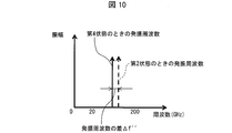
- FIG. 7 is a diagram showing a fourth state in which the device under test 72 is attached to the surface of the sensor IC 1 of the sensor device 100 shown in FIG.
- the state of water related to the object to be inspected 70 changes with the passage of time or the like (for example, increase or decrease in bulk water due to a change in the hydration state, and inclusion of the object 70 to be inspected). Evaporation of water to be used).
- the inspected object 70 is changed to the inspected object 72.
- the inspected object 72 has a portion 73, a portion 74, and a portion 75 whose physical properties are locally changed.
- the local change in the physical property of the inspection object 72 is, for example, a change in a chemical reaction of components included in the inspection object 72, a temperature change of the inspection object 72, a distance from the surface of the semiconductor substrate 10, or the like.
- the detection circuit 3 is driven by the control circuit 4 in the state (fourth state) in which the inspection object 72 is attached to the surface of the sensor IC 1 as shown in FIG.
- the frequency of the signal output from the unit cell is measured, and the oscillation frequency of the oscillator 20 is calculated.
- FIG. 10 is a diagram showing the oscillation frequency of the oscillator 20 in the fourth state with respect to the second state in the sensor device 100 shown in FIG. Along with the change from the inspection object 70 to the inspection object 72, the oscillation frequency of the oscillator 20 also changes.
- the detection circuit 3 calculates a difference ⁇ f ′′ of the oscillation frequency of the oscillator 20 between the second state and the fourth state when driving. Based on the difference ⁇ f ′′ in the oscillation frequency, it is possible to detect a local change of the inspection object 72 in the vicinity of the unit cell. For example, when a plurality of threshold values are provided and the oscillation frequency difference ⁇ f ′′ is greater than or equal to the first threshold value and less than the second threshold value, the device 72 is present in the vicinity of the unit cell, but the parts 73 to 75 are present.
- the local change of the inspection object 72 is associated with the arrangement of the plurality of unit cells A11 to ALM on the semiconductor substrate 10 by associating the local change of the inspection object 72 in the vicinity of each of the unit cells A11 to ALM. Can be detected. Therefore, since the sensor device 100 can individually detect the local change of the inspected object 72 for each of the unit cells A11 to ALM, the sensor device 100 has a resolution corresponding to the distribution density (arrangement density) of the unit cells A11 to ALM. The distribution of local changes of the inspection object 72 can be detected.
- Embodiment 4 of the present invention will be described below with reference to FIG.
- members having the same functions as those described in the embodiment are given the same reference numerals, and descriptions thereof are omitted.
- FIG. 11 is a schematic diagram for explaining the control for sequentially driving the unit cells A11 to ALM included in the sensor device 100 shown in FIG.
- the control circuit 4 drives the unit cell Axy (x is an integer from 1 to L, y is an integer from 1 to M) at time T_ (x ⁇ 1) L + y, and does not drive at other times. Output a control signal. Therefore, as shown in FIG. 11, from time T_1 to time T_ML, unit cell A11, unit cell A21, unit cell A31,..., Unit cell AL1, unit cell A21, unit cell A22,.
- the drive is sequentially performed at a predetermined time width and a predetermined time interval.
- the time interval for driving the unit cells A11 to ALM is preferably 1 millisecond or more.
- the temporal change of the oscillation frequency of each oscillator 20 of the unit cells A11 to ALM can be detected by repeating the sequential driving periodically or aperiodically.
- control by the control circuit 4 is flexible so that when the sequential driving is repeated, the intensive unit cells can be repeatedly driven or the intensive unit cell driving time can be extended. Also good. As a result, for example, by intensively driving the unit cell having a large change in the oscillation frequency, the distribution of the temporal change in the oscillation frequency of the oscillator 20 of each of the unit cells A11 to ALM can be detected with higher accuracy. it can.
- the sensor device 100 can sequentially detect a temporal change and a spatial change of the oscillation frequency of each oscillator 20 from the plurality of unit cells A11 to ALM.
- the temporal change and the spatial change of the oscillation frequency of the oscillator 20 are the local change and the temporal change of the property and state of the inspection object such as the parts 73 to 75 of the inspection object 72 shown in FIG. Due to changes.
- the sensor device 100 can sequentially detect a temporal change and a spatial change of the object to be inspected so as to change the oscillation frequency of the oscillator 20.
- test objects 70 to 72 are attached to a part of the surface of the sensor IC 1 of the sensor device 100 has been described.
- a case where the entire surface of the sensor IC 2 of the sensor device is immersed in an aqueous solution (inspected objects 76 and 77) will be described.
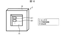
- FIG. 12 is a perspective view showing a schematic configuration of another sensor IC 2 included in the sensor device 100 shown in FIG. Moreover, it is a figure which shows the 1st state where the surface of sensor IC2 is clean.
- the sensor IC 2 is a sensor integrated circuit (Integrated Circuit).
- the sensor IC 2 includes a semiconductor substrate 10, a plurality of unit cells A11 to ALM, and further includes a sealing material 16.
- the sealing material 16 seals the bonding wire and the bonding pad so that the bonding wire and the bonding pad (not shown) are not in direct contact with the aqueous solution.
- the material and shape of the sealing material 16 are not particularly limited.
- the resonator 50 (at least one of the inductor 52 and the capacitor 54). ) Is formed on the uppermost metal layer. Further, as shown in FIG. 2B, the portion of the resonator 50 (at least one of the inductor 52 and the capacitor 54) formed in the metal layer which is the uppermost layer is covered with the protective film 15, and the aqueous solution ( There is no direct contact with the inspected objects 76 and 77).
- the control circuit 4 sequentially drives the unit cells A11 to ALM, and sets the frequency of the signal output by the driving unit cell.
- the detection circuit 3 measures. Then, the detection circuit 3 calculates the oscillation frequency of the oscillator 20 based on the frequency division ratio 1 / N of the frequency divider 30.
- FIG. 13 is a diagram showing a second state in which the surface of the sensor IC 2 shown in FIG.
- the inspection object 76 uniformly covers the surface of the semiconductor substrate 10 and is an aqueous solution.
- the control circuit 4 sequentially drives the unit cells A11 to ALM to drive the unit cells.
- the detection circuit 3 measures the frequency of the signal output from. Then, the detection circuit 3 calculates the oscillation frequency of the oscillator 20 based on the frequency division ratio 1 / N of the frequency divider 30.
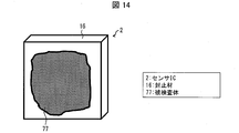
- FIG. 14 is a diagram illustrating a third state in which the surface of the sensor IC 2 illustrated in FIG.
- the inspection object 77 is an aqueous solution in which the inspection object 76 is changed.
- the change from the test object 76 to the test object 77 is, for example, a change in the properties of the aqueous solution due to a change in solute (e.g., change in concentration, vaporization, solidification, progress of chemical reaction, etc.) over time.
- the control circuit 4 sequentially drives the unit cells A11 to ALM to drive the unit cells.
- the detection circuit 3 measures the frequency of the signal output from. Then, the detection circuit 3 calculates the oscillation frequency of the oscillator 20 based on the frequency division ratio 1 / N of the frequency divider 30.
- FIG. 15 is a diagram showing the oscillation frequencies of the oscillator 20 in the first state, the second state, and the third state in the sensor IC 2 shown in FIG.
- the detection circuit 3 includes a difference ⁇ f ′′ ′′ of the oscillation frequency of the oscillator 20 between the first state and the second state, and a difference of the oscillation frequency of the oscillator 20 between the second state and the third state. ⁇ f ′ ′′ ′′ is calculated.
- the detection circuit 3 can calculate the distribution and average value of the property (physical properties) of the device under test 76 as a change in dielectric constant based on the difference ⁇ f ′ ′′ between the first state and the second state and the oscillation frequency. .
- the distribution of properties (physical properties) and the average value of the inspected object 77 can be calculated as changes in dielectric constant.
- a sensor device (sensor IC1, sensor IC2, sensor device 100) according to aspect 1 of the present invention includes a substrate (semiconductor substrate 10) and a plurality of resonators (50) disposed on the substrate, Each of the resonators changes the resonance frequency in accordance with the physical properties (properties, state, dielectric constant, etc.) of the inspected objects (70 to 72, 76, 77) in the vicinity of each of the resonators, and distributes the plurality of resonators. And a distribution of physical properties of the object to be inspected based on the resonance frequencies of the plurality of resonators, and the center of two resonators adjacent to each other among the plurality of resonators (50).
- the distance (row interval, column interval) is 300 ⁇ m or less.
- the resonator is not a narrowly-defined antenna that transmits and receives electromagnetic waves, and is not restricted by the aperture diameter depending on the wavelength, so that the area can be reduced.
- substrate can be raised by the area reduction of a resonator. Therefore, it is possible to detect the distribution of physical properties of the object to be inspected in a wide range and increase the spatial resolution. Since the spatial resolution is high in a wide range, a local change in physical properties of the object to be inspected can be detected in a wide range.
- the object to be inspected need not be labeled with magnetic particles or the like. For this reason, the measurement work can be simplified.
- the arrangement density of the resonators can be increased. For this reason, the sensor device can be miniaturized. Alternatively, the spatial resolution of the sensor device can be increased.
- a sensor device (sensor IC1, sensor IC2, sensor device 100) according to aspect 2 of the present invention is the sensor device according to aspect 1, and at least one of the plurality of resonators (50) includes an inductor ( 52) and a capacitor (54), and at least one of the inductor and the capacitor is formed in the metal layer of the substrate (10) and the substrate and the device under test (70 to 72). , 76, 77) including the layer closest to the contact position.
- the metal layer closest to the object to be inspected is sensitive to changes in the dielectric constant or permeability of the surface of the substrate, the resonance frequency is likely to change depending on the object to be inspected. For this reason, the sensitivity of the sensor device can be increased.
- the sensor device (sensor IC1, sensor IC2, sensor device 100) according to aspect 3 of the present invention is the sensor device according to aspect 1 or 2, and the resonance frequency of each of the plurality of resonators is 30 GHz or more and 200 GHz or less. It is characterized by being.
- the change in complex permittivity due to the hydration phenomenon is large. For this reason, according to the said structure, the motion of the water molecule inside a to-be-inspected object, a hydration phenomenon, etc. can be measured.
- a sensor device (sensor IC1, sensor IC2, sensor device 100) according to aspect 4 of the present invention is the sensor device according to any one of aspects 1 to 3, and at least of the plurality of resonators (50).
- the size of one resonator in plan view is a size that fits in a square having a side of 200 ⁇ m.
- the arrangement density of the resonators can be increased. For this reason, the sensor device can be miniaturized. Alternatively, the spatial resolution of the sensor device can be increased.
- a sensor device (100) according to aspect 5 of the present invention is the sensor device according to any one of aspects 1 to 4, and is provided in a one-to-one correspondence with each of the plurality of resonators (50).
- a plurality of frequency dividers (30) for dividing the resonance frequency of the corresponding resonator, and detection for estimating the resonance frequency of each of the plurality of resonators based on outputs of the plurality of frequency dividers And a circuit (3).
- the frequency band of the signal handled by the detection circuit is a frequency band lower than the resonance frequency band. Therefore, the detection circuit need not be configured to handle a high frequency band, and the detection circuit can be simplified and reduced in cost.
- a sensor device (sensor device 100) according to Aspect 6 of the present invention is the sensor device according to any one of Aspects 1 to 5, and includes a control circuit (4) for sequentially driving the plurality of resonators (50). It is further provided with the feature.
Landscapes
- Physics & Mathematics (AREA)
- Chemical & Material Sciences (AREA)
- General Physics & Mathematics (AREA)
- Health & Medical Sciences (AREA)
- Life Sciences & Earth Sciences (AREA)
- Analytical Chemistry (AREA)
- Biochemistry (AREA)
- General Health & Medical Sciences (AREA)
- Immunology (AREA)
- Pathology (AREA)
- Electrochemistry (AREA)
- Chemical Kinetics & Catalysis (AREA)
- Electromagnetism (AREA)
- Investigating Or Analyzing Materials By The Use Of Electric Means (AREA)
Abstract
L'objectif de la présente invention est d'améliorer la résolution spatiale et de détecter des variations localisées dans les propriétés physiques d'un objet d'examen. Un CI de capteur (1) comprend un substrat à semi-conducteur (10) et une pluralité d'oscillateurs (20) pourvus de résonateurs, et les résonateurs de chaque oscillateur de la pluralité d'oscillateurs (20) sont conçus pour faire varier la fréquence de résonance de ceux-ci en fonction des propriétés physiques de l'objet d'examen dans le voisinage de celui-ci, la distribution des propriétés physiques de l'objet d'examen est détectée sur la base de la fréquence de résonance et de la distribution des résonateurs de la pluralité d'oscillateurs (20), et la distance entre les centres de deux de la pluralité de résonateurs (20) qui sont contigus l'un à l'autre ne dépasse pas 300 µm.
Applications Claiming Priority (2)
| Application Number | Priority Date | Filing Date | Title |
|---|---|---|---|
| JP2015-139938 | 2015-07-13 | ||
| JP2015139938 | 2015-07-13 |
Publications (1)
| Publication Number | Publication Date |
|---|---|
| WO2017010177A1 true WO2017010177A1 (fr) | 2017-01-19 |
Family
ID=57756897
Family Applications (1)
| Application Number | Title | Priority Date | Filing Date |
|---|---|---|---|
| PCT/JP2016/065773 Ceased WO2017010177A1 (fr) | 2015-07-13 | 2016-05-27 | Capteur |
Country Status (1)
| Country | Link |
|---|---|
| WO (1) | WO2017010177A1 (fr) |
Cited By (4)
| Publication number | Priority date | Publication date | Assignee | Title |
|---|---|---|---|---|
| WO2017175879A1 (fr) * | 2016-04-05 | 2017-10-12 | シャープ株式会社 | Dispositif de capteur, procédé de détection et unité de capteur |
| JP2017187463A (ja) * | 2016-04-05 | 2017-10-12 | シャープ株式会社 | センサ装置、検出方法、及びセンサユニット |
| JP2021503069A (ja) * | 2017-10-16 | 2021-02-04 | サントル ナシオナル ドゥ ラ ルシェルシェ シアンティフィクCentre National De La Recherche Scientifique | 高電子移動度トランジスタおよびリング共振器を備えたセンサセルを有する検出センサ |
| US10976651B2 (en) | 2016-10-12 | 2021-04-13 | Sony Corporation | Image display apparatus and light source apparatus |
Citations (3)
| Publication number | Priority date | Publication date | Assignee | Title |
|---|---|---|---|---|
| JPH07306172A (ja) * | 1994-05-12 | 1995-11-21 | Mitsubishi Electric Corp | 燃料の混合比率検知装置 |
| JP2011513755A (ja) * | 2008-03-07 | 2011-04-28 | カリフォルニア インスティテュート オブ テクノロジー | 磁性粒子検出を基本とする実効インダクタンスの変化 |
| WO2014130023A1 (fr) * | 2013-02-20 | 2014-08-28 | Empire Technology Development Llc | Capteurs à nanotubes pour solutions conductrices |
-
2016
- 2016-05-27 WO PCT/JP2016/065773 patent/WO2017010177A1/fr not_active Ceased
Patent Citations (3)
| Publication number | Priority date | Publication date | Assignee | Title |
|---|---|---|---|---|
| JPH07306172A (ja) * | 1994-05-12 | 1995-11-21 | Mitsubishi Electric Corp | 燃料の混合比率検知装置 |
| JP2011513755A (ja) * | 2008-03-07 | 2011-04-28 | カリフォルニア インスティテュート オブ テクノロジー | 磁性粒子検出を基本とする実効インダクタンスの変化 |
| WO2014130023A1 (fr) * | 2013-02-20 | 2014-08-28 | Empire Technology Development Llc | Capteurs à nanotubes pour solutions conductrices |
Non-Patent Citations (4)
| Title |
|---|
| HUA WANG ET AL.: "A Frequency-Shift Based CMOS Magnetic Biosensor with Spatially Uniform Sensor Transducer Gain", IEEE CUSTOM INTEGRATED CIRCUITS CONFERENCE (CICC, 2010, pages 1 - 4, XP031786843 * |
| M. ABIDI ET AL.: "Sensing Liquid Properties Using Split-Ring Resonator in Mm-wave Band", IECON 2010 - 36TH ANNUAL CONFERENCE ON IEEE INDUSTRIAL ELECTRONICS SOCIETY, 2010, XP031840552 * |
| S. GUHA ET AL.: "An 8 GHz CMOS Near Field Bio- sensor Array for Imaging Spatial Permittivity Distribution of Biomaterials", 2014 IEEE MTT-S INTERNATIONAL MICROWAVE SYMPOSIUM (IMS2014, 2014, pages 1 - 4, XP032615317 * |
| S. VEHRING ET AL.: "Permittivity Sensor based on 60 GHz Patch Antenna", 2015 GERMAN MICROWAVE CONFERENCE, 16 March 2015 (2015-03-16), pages 311 - 314, XP032776451 * |
Cited By (6)
| Publication number | Priority date | Publication date | Assignee | Title |
|---|---|---|---|---|
| WO2017175879A1 (fr) * | 2016-04-05 | 2017-10-12 | シャープ株式会社 | Dispositif de capteur, procédé de détection et unité de capteur |
| JP2017187463A (ja) * | 2016-04-05 | 2017-10-12 | シャープ株式会社 | センサ装置、検出方法、及びセンサユニット |
| US10690611B2 (en) | 2016-04-05 | 2020-06-23 | Sharp Kabushiki Kaisha | Sensor device, detection method, and sensor unit |
| US10976651B2 (en) | 2016-10-12 | 2021-04-13 | Sony Corporation | Image display apparatus and light source apparatus |
| JP2021503069A (ja) * | 2017-10-16 | 2021-02-04 | サントル ナシオナル ドゥ ラ ルシェルシェ シアンティフィクCentre National De La Recherche Scientifique | 高電子移動度トランジスタおよびリング共振器を備えたセンサセルを有する検出センサ |
| JP7100026B2 (ja) | 2017-10-16 | 2022-07-12 | サントル ナシオナル ドゥ ラ ルシェルシェ シアンティフィク | 高電子移動度トランジスタおよびリング共振器を備えたセンサセルを有する検出センサ |
Similar Documents
| Publication | Publication Date | Title |
|---|---|---|
| WO2017010177A1 (fr) | Capteur | |
| Thai et al. | Novel design of a highly sensitive RF strain transducer for passive and remote sensing in two dimensions | |
| US7830695B1 (en) | Capacitive arrangement for qubit operations | |
| US8047713B2 (en) | Plasmon resonance detector | |
| JP6416398B2 (ja) | センサ回路 | |
| US9291600B2 (en) | Piezoresistive NEMS array network | |
| KR20160010348A (ko) | 유전체 막 두께 모니터링용 커패시턴스 테스트 구조 및 커패시턴스 테스트 방법 | |
| JP6538186B2 (ja) | センサ回路 | |
| Steinbach et al. | Thermal kinetic inductance detectors for ground-based millimeter-wave cosmology | |
| Mohammed et al. | Analysis fin field-effect transistor design with high-k insulators | |
| Otxoa et al. | Quantum interference capacitor based on double-passage Landau-Zener-Stückelberg-Majorana interferometry | |
| Chen et al. | Hydrogen sensor based on Pd-functionalized film bulk acoustic resonator | |
| Lee et al. | Surface acoustic wave-based infrared sensor with aluminum nitride films deposited | |
| Mahmoodi et al. | Active frequency selective surface for strain sensing | |
| Pardue et al. | Integration of carbon nanotube films with SRRs for air quality sensing applications | |
| US8677830B2 (en) | Apparatus and method for acquiring mechanical loads on thrust elements | |
| Morris et al. | Embedded aperture-based FSS sensor | |
| Pecora et al. | Interdigitated sensorial system on flexible substrate | |
| Zhang et al. | A microwave sensor array for water quality testing | |
| JP6486740B2 (ja) | センサic | |
| Nakamoto et al. | Study of VHF-band QCM gas sensor | |
| Jana et al. | A dielectric modulated MOS transistor for biosensing | |
| Zhang et al. | Fast Thermodynamic Study on a Silicon Nanotransistor at Cryogenic Temperatures | |
| Huq et al. | Biodegradable Substrate based Printed Microwave Resonator for Liquid Sensing | |
| Aswani et al. | Comparative Study of Different Shapes of Parallel Plate Capacitor for Moisture |
Legal Events
| Date | Code | Title | Description |
|---|---|---|---|
| 121 | Ep: the epo has been informed by wipo that ep was designated in this application |
Ref document number: 16824157 Country of ref document: EP Kind code of ref document: A1 |
|
| NENP | Non-entry into the national phase |
Ref country code: DE |
|
| NENP | Non-entry into the national phase |
Ref country code: JP |
|
| 122 | Ep: pct application non-entry in european phase |
Ref document number: 16824157 Country of ref document: EP Kind code of ref document: A1 |