WO2017010227A1 - Dispositif de communication, procédé de communication et système de communication - Google Patents
Dispositif de communication, procédé de communication et système de communication Download PDFInfo
- Publication number
- WO2017010227A1 WO2017010227A1 PCT/JP2016/068062 JP2016068062W WO2017010227A1 WO 2017010227 A1 WO2017010227 A1 WO 2017010227A1 JP 2016068062 W JP2016068062 W JP 2016068062W WO 2017010227 A1 WO2017010227 A1 WO 2017010227A1
- Authority
- WO
- WIPO (PCT)
- Prior art keywords
- signal
- communication device
- communication
- modulation
- unit
- Prior art date
- Legal status (The legal status is an assumption and is not a legal conclusion. Google has not performed a legal analysis and makes no representation as to the accuracy of the status listed.)
- Ceased
Links
Images







Classifications
-
- H—ELECTRICITY
- H04—ELECTRIC COMMUNICATION TECHNIQUE
- H04B—TRANSMISSION
- H04B10/00—Transmission systems employing electromagnetic waves other than radio-waves, e.g. infrared, visible or ultraviolet light, or employing corpuscular radiation, e.g. quantum communication
- H04B10/50—Transmitters
- H04B10/516—Details of coding or modulation
- H04B10/548—Phase or frequency modulation
- H04B10/556—Digital modulation, e.g. differential phase shift keying [DPSK] or frequency shift keying [FSK]
- H04B10/5563—Digital frequency modulation
-
- H—ELECTRICITY
- H04—ELECTRIC COMMUNICATION TECHNIQUE
- H04B—TRANSMISSION
- H04B5/00—Near-field transmission systems, e.g. inductive or capacitive transmission systems
- H04B5/20—Near-field transmission systems, e.g. inductive or capacitive transmission systems characterised by the transmission technique; characterised by the transmission medium
- H04B5/24—Inductive coupling
- H04B5/26—Inductive coupling using coils
- H04B5/266—One coil at each side, e.g. with primary and secondary coils
-
- H—ELECTRICITY
- H04—ELECTRIC COMMUNICATION TECHNIQUE
- H04B—TRANSMISSION
- H04B5/00—Near-field transmission systems, e.g. inductive or capacitive transmission systems
- H04B5/40—Near-field transmission systems, e.g. inductive or capacitive transmission systems characterised by components specially adapted for near-field transmission
- H04B5/45—Transponders
-
- H—ELECTRICITY
- H04—ELECTRIC COMMUNICATION TECHNIQUE
- H04W—WIRELESS COMMUNICATION NETWORKS
- H04W52/00—Power management, e.g. Transmission Power Control [TPC] or power classes
- H04W52/04—Transmission power control [TPC]
- H04W52/06—TPC algorithms
- H04W52/08—Closed loop power control
-
- H—ELECTRICITY
- H04—ELECTRIC COMMUNICATION TECHNIQUE
- H04W—WIRELESS COMMUNICATION NETWORKS
- H04W52/00—Power management, e.g. Transmission Power Control [TPC] or power classes
- H04W52/04—Transmission power control [TPC]
- H04W52/06—TPC algorithms
- H04W52/10—Open loop power control
-
- H—ELECTRICITY
- H04—ELECTRIC COMMUNICATION TECHNIQUE
- H04W—WIRELESS COMMUNICATION NETWORKS
- H04W52/00—Power management, e.g. Transmission Power Control [TPC] or power classes
- H04W52/04—Transmission power control [TPC]
- H04W52/38—TPC being performed in particular situations
- H04W52/42—TPC being performed in particular situations in systems with time, space, frequency or polarisation diversity
-
- H—ELECTRICITY
- H04—ELECTRIC COMMUNICATION TECHNIQUE
- H04W—WIRELESS COMMUNICATION NETWORKS
- H04W88/00—Devices specially adapted for wireless communication networks, e.g. terminals, base stations or access point devices
- H04W88/02—Terminal devices
- H04W88/021—Terminal devices adapted for Wireless Local Loop operation
-
- H—ELECTRICITY
- H04—ELECTRIC COMMUNICATION TECHNIQUE
- H04B—TRANSMISSION
- H04B5/00—Near-field transmission systems, e.g. inductive or capacitive transmission systems
- H04B5/20—Near-field transmission systems, e.g. inductive or capacitive transmission systems characterised by the transmission technique; characterised by the transmission medium
- H04B5/24—Inductive coupling
- H04B5/26—Inductive coupling using coils
Definitions
- the present disclosure relates to a communication device used in near field communication (NFC), a communication method used in such a communication device, and a communication system including such a communication device.
- NFC near field communication
- NFC Short-range wireless communication standards
- NFC standards have compatibility as a so-called upward compatibility with various standards such as Type A standards, Type B standards, FeliCa (registered trademark) standards, and ISO 15693 standards. . That is, for example, a reader / writer or card that conforms to the NFC standard also conforms to all these standards.
- the reader / writer transmits data to the card by ASK (Amplitude Shift Keying) modulation, and the card transmits data to the reader / writer by load modulation.
- ASK Amplitude Shift Keying
- Patent Documents 1 and 2 disclose a communication device that can perform communication by load modulation (passive load modulation).
- PLL phase locked loop
- the communication device includes a phase synchronization unit, a modulation unit, and a control unit.
- the phase synchronization unit generates a second signal based on a first signal received from a communication partner by selectively performing a closed loop operation or an open loop operation.
- the modulation unit is configured to be able to modulate the first signal based on the second signal.
- the control unit controls operations of the phase synchronization unit and the modulation unit.
- the second signal is generated based on the first signal received from the communication partner by selectively causing the phase synchronization unit to perform the closed-loop operation or the open-loop operation.
- the modulation unit modulates the first signal based on the second signal.
- the communication system includes a first communication device and a second communication device.
- the first communication device transmits the first signal.
- the second communication device includes a phase synchronization unit, a modulation unit, and a control unit.
- the phase synchronization unit generates a second signal based on the first signal received from the first communication device by selectively performing a closed loop operation or an open loop operation.
- the modulation unit is configured to be able to modulate the first signal based on the second signal.
- the control unit controls operations of the phase synchronization unit and the modulation unit.
- the phase synchronization unit In the communication device, the communication method, and the communication system according to the embodiment of the present disclosure, the phase synchronization unit generates the second signal based on the first signal received from the communication partner. Based on the second signal, the first signal is modulated. In the phase synchronization unit, a closed loop operation or an open loop operation is selectively performed.
- the phase synchronization unit selectively performs the closed loop operation or the open loop operation, so that the communication quality can be improved.
- the effect described here is not necessarily limited, and there may be any effect described in the present disclosure.
- FIG. 1 is a block diagram illustrating a configuration example of a communication system according to an embodiment of the present disclosure.
- FIG. 2 is a block diagram illustrating a configuration example of a phase synchronization unit illustrated in FIG. 1.
- FIG. 6 is a timing waveform diagram illustrating an operation example of the signal generation unit according to the first embodiment. It is a schematic diagram for demonstrating the concept of active load modulation.
- FIG. 6 is a timing waveform diagram illustrating an operation example of the communication system according to the first embodiment.
- FIG. 10 is a timing waveform chart illustrating another operation example of the communication system according to the first embodiment.
- FIG. 2 is a characteristic diagram illustrating a characteristic example of the communication system illustrated in FIG. 1.
- FIG. 1 is a block diagram illustrating a configuration example of a communication system according to an embodiment of the present disclosure.
- FIG. 2 is a block diagram illustrating a configuration example of a phase synchronization unit illustrated in FIG. 1.
- FIG. 6 is a timing waveform diagram illustrating
- FIG. 10 is a timing waveform diagram illustrating an operation example of a signal generation unit according to a modification of the first embodiment. It is a block diagram showing the example of 1 structure of the communication system which concerns on the other modification of 1st Embodiment. It is a flowchart showing the operation example of the communication system which concerns on the other modification of 1st Embodiment. It is a flowchart showing the operation example of the communication system which concerns on the other modification of 1st Embodiment. It is a block diagram showing the example of 1 structure of the communication system which concerns on the other modification of 1st Embodiment. It is a flowchart showing the operation example of the communication system which concerns on the other modification of 1st Embodiment.
- FIG. 10 is a timing waveform diagram illustrating an operation example of a signal generation unit according to a modification of the second embodiment.
- FIG. 1 illustrates a configuration example of a communication system 1 including a communication device according to the first embodiment.
- the communication system 1 performs communication by short-range wireless communication.
- the communication method according to the embodiment of the present disclosure is embodied by the present embodiment, and will be described together.
- the communication system 1 includes a communication device 10 and a communication device 20.
- the communication device 10 and the communication device 20 communicate with each other via a magnetic field.
- a coil 15 (described later) of the communication device 10 and a coil 21 (described later) of the communication device 20 are coupled via a magnetic field, so that data is transmitted and received by electromagnetic induction. ing.
- the communication device 10 transmits data to the communication device 20 by ASK modulation, and the communication device 20 transmits data to the communication device 10 by so-called active load modulation.
- the communication apparatus 10 is applied to a reader / writer, for example, and conforms to any one of various standards such as Type A standard, Type B standard, FeliCa standard, and ISO 15693 standard.
- the communication device 20 is applied to, for example, a card and conforms to the NFC standard that is upward compatible with these standards.
- the communication device 10 includes a carrier signal generation unit 11, a data generation unit 12, a modulation unit 13, an amplifier 14, a coil 15, a capacitor 16, and a demodulation unit 17.
- the carrier signal generator 11 generates a carrier signal.
- the frequency of the carrier signal is, for example, 13.56 MHz.
- the data generation unit 12 generates data D1 to be transmitted.
- the modulating unit 13 generates a signal SIG11 by modulating the carrier signal by ASK modulation using the data D1.
- the amplifier 14 generates a signal SIG12 based on the signal SIG11, and outputs the signal SIG12 as a signal between the first output terminal and the second output terminal.
- a first output terminal of the amplifier 14 is connected to one end of the coil 15 and one end of the capacitor 16.
- the second output terminal of the amplifier 14 is connected to the other end of the coil 15 and the other end of the capacitor 16.
- the coil 15 generates a magnetic field based on the signal SIG12, and is coupled to a coil 21 (described later) of the communication device 20 via a magnetic field.
- One end of the coil 15 is connected to the first output terminal of the amplifier 14 and one end of the capacitor 16, and the other end is connected to the second output terminal of the amplifier 14 and the other end of the capacitor 16.
- One end of the capacitor 16 is connected to one end of the coil 15 and the first output terminal of the amplifier 14, and the other end is connected to the other end of the coil 15 and the second output terminal of the amplifier 14.
- the demodulator 17 receives the data D2 transmitted from the communication device 20 by performing a demodulation operation based on the signal at the other end of the coil 15, for example, so-called I / Q (In-phase / Quadrature). It is configured using a demodulator.
- the communication device 20 performs communication by load modulation when transmitting data to the communication device 10. Specifically, during a period in which the communication device 10 is transmitting a carrier signal to the communication device 20, the communication control unit 28 (described later) of the communication device 20 determines the communication device 10 according to the data D2 to be transmitted. Change the load as seen. This change in load appears as a change in the amplitude or phase of the voltage signal at the other end of the coil 15 in the communication device 10, for example.
- the demodulator 17 receives the data D2 transmitted from the communication device 20 by detecting the amplitude and phase of the voltage signal at the other end of the coil 15. The demodulator 17 supplies the data D2 to other blocks in the communication device 10.
- the demodulator 17 is operated based on the signal at the other end of the coil 15, but is not limited to this.
- the demodulator 17 may operate based on a signal at one end of the coil 15 or may operate based on a signal between both ends of the coil 15.
- the communication device 20 includes a coil 21, a capacitor 22, a phase synchronization unit 30, amplifiers 24A and 24B, switches 23A and 23B, a data generation unit 27, a communication control unit 28, a signal generation unit 29, and a demodulation. Part 26.
- the coil 21 is coupled to the coil 15 of the communication device 10 via a magnetic field, and generates a signal SIG21 corresponding to the signal SIG12 in the communication device 10 by electromagnetic induction.
- One end of the coil 21 is connected to one end of the capacitor 22 and one end of the switch 23A, and the other end is connected to the other end of the capacitor 22 and one end of the switch 23B.
- One end of the capacitor 22 is connected to one end of the coil 21 and one end of the switch 23A, and the other end is connected to the other end of the coil 21 and one end of the switch 23B.
- the phase synchronization unit 30 generates the signal SIG30 based on the signal Sin at the other end of the coil 21, and is configured using a PLL (Phase Locked Loop).
- PLL Phase Locked Loop
- FIG. 2 shows a configuration example of the phase synchronization unit 30.
- the phase synchronization unit 30 includes a PFD (Phase Frequency Detector) 31, a charge pump 32, a switch 33, a loop filter 34, and a VCO (VoltageCOControlled Oscillator) 35.
- PFD Phase Frequency Detector
- VCO VoltageCOControlled Oscillator
- the PFD 31 compares the phase of the signal Sin with the phase of the signal SIG30 output from the VCO 35.
- the charge pump 32 selectively supplies current to the loop filter 34 or sinks current from the loop filter 34 based on the comparison result in the PFD 31.
- the output terminal of the charge pump 32 is connected to the input terminal of the loop filter 34 via the switch 33.
- the switch 33 is connected to the output terminal of the charge pump 32 and the input terminal of the loop filter 34 when turned on, and is turned on / off based on the loop control signal CT2.
- the loop filter 34 is for determining a loop response characteristic in the phase synchronization unit 30, an input terminal is connected to the output terminal of the charge pump 32 via the switch 33, and an output terminal is connected to the input terminal of the VCO 35.
- the VCO 35 generates a signal SIG30 by oscillating at a frequency corresponding to the output voltage of the loop filter 34.
- the phase synchronization unit 30 generates the signal SIG30 based on the signal Sin. At that time, the phase synchronization unit 30 can selectively perform an open loop operation or a closed loop operation based on the loop control signal CTL2.
- the amplifier 24A (FIG. 1) amplifies the signal SIG30 and outputs the amplified signal.
- the amplifier 24B inverts and amplifies the signal SIG30 and outputs an inverted and amplified signal.
- One end of the switch 23A is connected to one end of the coil 21 and one end of the capacitor 22, and the other end is connected to the output terminal of the amplifier 24A.
- One end of the switch 23B is connected to the other end of the coil 21 and the other end of the capacitor 22, and the other end is connected to the output terminal of the amplifier 24B.
- the switches 23A and 23B are turned on / off based on the modulation control signal CTL1.
- the communication device 20 performs active load modulation by turning on and off the switches 23A and 23B based on the modulation control signal CTL1.
- the data generation unit 27 generates data D2 to be transmitted and supplies the data D2 to the communication control unit 28.
- the communication control unit 28 generates a modulation control signal CTL1 based on the data D2, supplies the modulation control signal CTL1 to the switches 23A and 23B, and supplies it to the signal generation unit 29.
- the signal generation unit 29 generates a loop control signal CTL2 based on the modulation control signal CTL1, and supplies the loop control signal CTL2 to the phase synchronization unit 30.
- FIG. 3 shows an operation example of the signal generation unit 29, where (A) shows the waveform of the modulation control signal CTL1, and (B) shows the waveform of the loop control signal CTL2.
- the switches 23A and 23B are turned off during a period in which the modulation control signal CTL1 is at a low level, and turned on in a period in which the modulation control signal CTL1 is at a high level.
- the phase synchronization unit 30 performs a closed loop operation during a period in which the loop control signal CTL2 is at a low level, and performs an open loop operation in a period in which the loop control signal CTL2 is at a high level.
- the signal generation unit 29 changes the loop control signal CTL2 from the low level to the high level in response to the rise.
- the signal generation unit 29 sets the loop control signal CTL2 to the high level at the timing t3 when a predetermined time has elapsed from the falling timing t2 in response to the falling. From low to low.
- the signal generation unit 29 generates the loop control signal CTL2 having a pulse width longer than that of the modulation control signal CTL1 by delaying the falling timing of the modulation control signal CTL1 by the shift amount ⁇ t.
- the phase synchronization unit 30 performs an open loop operation in a period (period t1 to t3) corresponding to the period t1 to t2 in which the switches 23A and 23B are turned on.
- the rising timing of the loop control signal CTL2 is equal to the rising timing of the modulation control signal CTL1, but the present invention is not limited to this.
- the rising timing of the loop control signal CTL2 may be delayed by a circuit delay from the rising timing of the modulation control signal CTL1.
- the rising timing of the loop control signal CTL2 is the modulation control signal CTL1 only for the time required for circuit operation such as the setup time. It may be later than the rise timing.
- the demodulator 26 receives data D1 transmitted from the communication device 10 by performing a demodulation operation based on the signal Sin at the other end of the coil 21, and is configured using an ASK demodulator. Is.
- the demodulator 26 supplies the data D1 to other blocks in the communication device 20.
- phase synchronizer 30 and the demodulator 26 are operated based on the signal Sin at the other end of the coil 21, but the present invention is not limited to this.
- the phase synchronization unit 30 and the demodulation unit 26 may be operated based on a signal at one end of the coil 21 or may be operated based on a signal between both ends of the coil 21.
- the communication device 20 corresponds to a specific example of “communication device” in the present disclosure.
- the amplifiers 24A and 24B and the switches 23A and 23B correspond to a specific example of “modulation unit” in the present disclosure.
- the communication control unit 28 and the signal generation unit 29 correspond to a specific example of “control unit” in the present disclosure.
- the communication device 10 transmits data D1 to the communication device 20 by ASK modulation. Specifically, in the communication device 10, first, the carrier signal generation unit 11 generates a carrier signal, and the data generation unit 12 generates data D1 to be transmitted.
- the modulation unit 13 generates a signal SIG11 by modulating the carrier signal by ASK modulation using the data D1.
- the amplifier 14 generates a signal SIG12 based on the signal SIG11.
- the coil 15 generates a magnetic field based on the signal SIG12.
- the coil 21 generates a signal SIG21 based on the magnetic field generated by the coil 15.
- the demodulator 26 receives the data D1 transmitted from the communication device 10 by performing a demodulation operation based on the signal Sin at the other end of the coil 21.
- the communication device 20 transmits data D2 to the communication device 10 by active load modulation. Specifically, first, during a period in which the communication device 10 transmits a carrier signal to the communication device 20, the communication control unit 28 generates the modulation control signal CTL1 based on the data D2. The signal generator 29 generates a loop control signal CTL2 based on the modulation control signal CTL1. The phase synchronization unit 30 selectively performs an open loop operation or a closed loop operation based on the loop control signal CTL2, and generates a signal SIG30 based on the signal Sin. The amplifier 24A amplifies the output signal SIG30 of the phase synchronization unit 30 and outputs the amplified signal.
- the amplifier 24B inverts and amplifies the output signal SIG30 of the phase synchronization unit 30, and outputs an inverted and amplified signal.
- the switches 23A and 23B are turned on / off based on the modulation control signal CTL1. Thereby, the load seen from the communication apparatus 10 changes according to the data D2.
- the demodulator 17 of the communication device 10 receives the data D2 transmitted from the communication device 20 by performing a demodulation operation based on the signal at the other end of the coil 15.
- the communication device 20 transmits data D2 to the communication device 10 by so-called active load modulation.
- active load modulation will be described in detail.
- the communication control unit 28 turns on and off the switches 23A and 23B according to the data D2 during a period in which the communication device 10 transmits a carrier signal to the communication device 20.
- the switches 23A and 23B are turned on, the output signal of the amplifier 24A is supplied to one end of the coil 21 and the output signal of the amplifier 24B is supplied to the other end of the coil 21.
- the coil 21 generates a magnetic field.
- the coil 21 of the communication device 20 generates a magnetic field during the period in which the communication device 10 transmits a carrier signal to the communication device 20, thereby greatly changing the magnetic field.
- the load viewed from the communication device 10 can be greatly changed.
- the demodulator 17 of the communication device 10 receives the data D2 transmitted from the communication device 20 by performing a demodulation operation based on the load change.
- the communication distance can be extended, or the antennas (coils 15, 21) can be downsized.
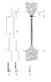
- FIG. 3 schematically shows the operation of active load modulation.
- the coil 15 of the communication device 10 generates a magnetic field based on the carrier signal W1
- the coil 21 of the communication device 20 generates a magnetic field based on the signal W2 synchronized with the carrier signal in a period in which the switches 23A and 23B are turned on. Is generated.
- the demodulation unit 17 of the communication device 10 performs a demodulation operation based on the combined signal W3 of the carrier signal W1 and the signal W2.
- This combined signal W3 can be expressed as follows.
- the first term on the left side represents the carrier signal W1
- the second term on the left side represents the signal W2.
- the synthesized signal W3 can be expressed using a sine wave synthesis theorem.
- the amplitude of this combined signal W3 varies depending on the amplitude A of the carrier signal W1, the amplitude B of the signal W2, and the phase ⁇ . Therefore, depending on the situation, the amplitude of the synthesized signal W3 may be extremely small.
- the amplitude of the signal Sin at the other end of the coil 21 is also reduced.
- the phase synchronization unit 30 performs an open loop operation in a period (an open loop operation period P2 described later) corresponding to a period during which active load modulation is performed (a modulation period P1 described later). To control. Thereby, in the communication apparatus 20, even when the amplitude of the signal Sin becomes small due to the active load modulation, the possibility that the phase synchronization unit 30 malfunctions can be reduced.
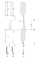
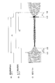
- FIG. 5 shows an operation example of the communication system 1, (A) shows the waveform of the modulation control signal CTL1, (B) shows the waveform of the loop control signal CTL2, and (C) shows the signal Sin. Waveform is shown.
- the communication device 20 performs active load modulation in the modulation period P1.
- the phase synchronization unit 30 performs an open loop operation in the open loop operation period P2 corresponding to the modulation period P1. This operation will be described in detail below.
- the communication control unit 28 of the communication device 20 sets the modulation control signal CTL1 to a low level (FIG. 5A). Thereby, the switches 23A and 23B are turned off. Therefore, the signal Sin corresponding to the carrier signal transmitted by the communication device 10 appears at the other end of the coil 21 (FIG. 5C). Further, the signal generator 29 sets the loop control signal CTL2 to a low level based on the modulation control signal CTL1 (FIG. 5B). Accordingly, the phase synchronization unit 30 performs a closed loop operation. That is, the phase synchronization unit 30 generates a signal SIG30 synchronized with the signal Sin based on the signal Sin.
- the communication control unit 28 changes the modulation control signal CTL1 from the low level to the high level at the timing t11 (FIG. 5A).
- the switches 23A and 23B are turned on, and the communication device 20 starts active load modulation.
- the signal generation unit 29 changes the loop control signal CTL2 from the low level to the high level based on the modulation control signal CTL1 (FIG. 5B).
- the phase synchronization unit 30 starts an open loop operation.
- the switch 33 is turned off.
- the loop filter 34 maintains the output voltage, the frequency of the output signal SIG30 of the phase synchronization unit 30 is maintained.
- the communication control unit 28 changes the modulation control signal CTL1 from the high level to the low level at timing t12 (FIG. 5A).
- the switches 23A and 23B are turned off.
- the amplitude of the signal Sin increases with a predetermined time constant and approaches the amplitude before the timing t11 (FIG. 5C).
- the signal generation unit 29 changes the loop control signal CTL2 from the high level to the low level at timing t13 when the time corresponding to the shift amount ⁇ t has elapsed from timing t12 (FIG. 5B).
- the phase synchronization unit 30 starts a closed loop operation.
- the communication device 20 transmits data D2 to the communication device 10 by repeating such an operation.
- phase synchronization unit 30 since the phase synchronization unit 30 performs the open loop operation in the open loop operation period P2 corresponding to the modulation period P1, the possibility that the phase synchronization unit 30 malfunctions can be reduced. it can.
- the phase synchronization unit 30 may malfunction if the amplitude of the signal Sin decreases during the modulation period P1. Specifically, when the amplitude of the signal Sin is extremely small, the PFD 31 of the phase synchronization unit 30 cannot detect the transition of the signal Sin, and thus cannot perform the phase comparison operation. As a result, the output voltage of the loop filter 34 gradually departs from the desired voltage, and as a result, the frequency of the signal SIG30 deviates from the desired frequency.
- the phase synchronization unit 30 may not be able to return the frequency of the signal SIG30 to a desired frequency even when the modulation period P1 ends and the amplitude of the signal Sin increases. Further, when the frequency is shifted in this manner, the frequency of the radio signal to be used may be out of the frequency band that can be used in short-range wireless communication, and the standard for short-range wireless communication may not be satisfied.
- the phase synchronization unit 30 performs the open loop operation in the open loop operation period P2 corresponding to the modulation period P1.
- the output voltage of the loop filter 34 is maintained because the switch 33 of the phase synchronization unit 30 is in the OFF state.
- the frequency of the signal SIG30 is maintained. Therefore, after that, when the phase synchronization unit 30 starts the closed loop operation, the phase synchronization unit 30 can more reliably synchronize the signal SIG30 with the signal Sin.
- the possibility that the phase synchronization unit 30 malfunctions can be reduced. As a result, communication quality can be improved in the communication system 1.
- the phase synchronization unit 30 when the signal generation unit 29 is not provided and the phase synchronization unit 30 is configured to selectively perform an open loop operation or a closed loop operation based on the modulation control signal CTL1, Closed loop operation is started at t12. At this time, since the amplitude of the signal Sin is still small immediately after the timing t12, the phase synchronization unit 30 may malfunction.
- the end timing of the open loop operation period P2 is made later than the end timing of the modulation period P1.
- the signal generation unit 29 generates the loop control signal CTL2 by delaying the falling timing of the modulation control signal CTL1 by the shift amount ⁇ t.
- the phase synchronization unit 30 starts the closed loop operation at the timing t13 when the amplitude of the signal Sin increases, so that the possibility that the phase synchronization unit 30 malfunctions can be reduced. As a result, communication quality can be improved in the communication system 1.
- FIG. 6 shows another example of the operation of the communication system 1.
- A shows the waveform of the modulation control signal CTL1
- B shows the waveform of the loop control signal CTL2
- C shows the signal Sin. The waveform is shown.
- the communication control unit 28 of the communication device 20 sets the modulation control signal CTL1 to a low level (FIG. 6A), and the signal generation unit 29 performs loop control.
- the signal CTL2 is set to a low level (FIG. 6B).
- a signal Sin corresponding to the carrier signal transmitted by the communication device 10 appears at the other end of the coil 21 (FIG. 6C).
- the communication control unit 28 changes the modulation control signal CTL1 from the low level to the high level at the timing t21 (FIG. 6A). Thereby, the switches 23A and 23B are turned on, and the communication device 20 starts active load modulation. At the same time, the signal generation unit 29 changes the loop control signal CTL2 from the low level to the high level based on the modulation control signal CTL1 (FIG. 6B). As a result, the phase synchronization unit 30 starts an open loop operation. In this example, when the switches 23A and 23B are turned on, the carrier signal transmitted by the communication device 10 and the signal SIG30 are combined, and the amplitude of the signal Sin increases with a predetermined time constant (FIG. 6 ( C)). Then, the amplitude of the signal Sin is kept large until the timing t22.
- the communication control unit 28 changes the modulation control signal CTL1 from the high level to the low level at timing t22 (FIG. 6A).
- the switches 23A and 23B are turned off.
- the amplitude of the signal Sin decreases with a predetermined time constant (FIG. 6C).
- the amplitude of the signal Sin becomes extremely small transiently as shown in the waveform W1, and then gradually increases and approaches the amplitude before the timing t21.
- the signal generation unit 29 changes the loop control signal CTL2 from the high level to the low level at timing t23 when the time corresponding to the shift amount ⁇ t has elapsed from timing t22 (FIG. 6B).
- the phase synchronization unit 30 starts a closed loop operation.
- the communication device 20 transmits data D2 to the communication device 10 by repeating such an operation.
- the amplitude of the signal Sin increases during the modulation period P1, and decreases after the modulation period P1 ends.
- the amplitude of the signal Sin becomes transiently extremely small.
- the end timing of the open loop operation period P2 is set to timing t23 after the waveform W1 appears.
- the phase synchronization unit 30 does not perform a closed-loop operation during a period in which the amplitude of the signal Sin is extremely small, so that the possibility of malfunctioning can be reduced.
- communication quality can be improved in the communication system 1.
- the signal generation unit 29 generates the loop control signal CTL2 by delaying the falling timing of the modulation control signal CTL1 by the shift amount ⁇ t.
- the communication distance can be extended by increasing the shift amount ⁇ t.
- FIG. 7 shows the communication characteristics of the communication system 1.
- the horizontal axis indicates the shift amount ⁇ t, and the vertical axis indicates the communication distance.
- the amplitude A of the carrier signal W1 shown in FIG. 4 is small. Therefore, the amplitude of the composite signal W3 changes according to the communication distance.
- the possibility that the phase synchronization unit 30 malfunctions can be reduced by increasing the shift amount ⁇ t.
- the communication distance can be extended by increasing the shift amount ⁇ t.
- phase synchronization unit since the phase synchronization unit performs the open loop operation in the open loop operation period corresponding to the load modulation, it is possible to reduce the possibility that the phase synchronization unit malfunctions. Communication quality can be improved.
- the end timing of the open loop operation period is made later than the end timing of the modulation period, so that the possibility that the phase synchronization unit malfunctions can be reduced, so that the communication quality can be improved.
- the communication distance can be extended by reducing the possibility that the phase synchronization unit malfunctions in this way.
- the signal generation unit 29 generates the loop control signal CTL2 by delaying the falling timing of the modulation control signal CTL1 by the shift amount ⁇ t.
- the shift amount ⁇ t may be configured to be changeable as shown in FIG.
- the signal generation unit 29A according to this modification can set the falling timing of the loop control signal CTL2 to any one of timings t31 to t38.
- the falling timing of the loop control signal CTL2 can be set to eight ways, but is not limited to this, and may be seven or less, or nine or more.
- the shift amount ⁇ t is fixed.
- the shift amount ⁇ t is not limited to this.
- the shift amount ⁇ t may be changed according to the communication state. Below, this modification is demonstrated in detail.
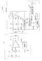
- FIG. 9 illustrates a configuration example of the communication system 1B according to the present modification.
- the communication system 1B includes a communication device 20B.
- the communication device 20B includes a demodulator 26B and a signal generator 29B.
- the demodulator 26B performs a demodulation operation based on the signal Sin at the other end of the coil 21, and determines a standard (communication standard SP) to which the communication device 10 complies.
- a standard communication standard SP
- the modulation degree of the signal transmitted from the communication device 10 can be used. That is, as described above, the communication device 10 conforms to any one of various standards such as Type A standard, Type B standard, FeliCa standard, ISO 15693 standard, and the modulation unit 13 of the communication device 10 ASK modulation is performed with a modulation degree corresponding to the standard that is compliant. Therefore, the demodulator 26B can determine the standard (communication standard SP) to which the communication device 10 is based on the modulation degree of the signal transmitted from the communication device 10.
- the demodulator 26B may determine the communication standard SP based on other characteristics of the signal (coding, bit rate, subcarrier), and the like. For example, when the data D1 transmitted by the communication device 10 includes information according to the communication standard SP, the demodulation unit 26B may determine the communication standard SP based on the information.
- the signal generation unit 29B is configured to be able to change the shift amount ⁇ t, and sets the shift amount ⁇ t based on the communication standard SP. is there.
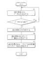
- FIG. 14 shows an operation example of the communication system 2B.
- the communication device 10 transmits data D1 to the communication device 20B.
- the communication device 20B responds by transmitting the data D2 to the communication device 10. This operation will be described in detail below.
- the communication device 10 transmits data D1 to the communication device 20B by ASK modulation (step S1).
- the demodulation unit 26B of the communication device 20B confirms whether or not the data D1 has been received (step S2).
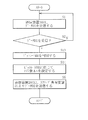
- the data generator 27 of the communication device 20B generates data D2 for responding to the communication device 10, and proceeds to step S3. If the demodulator 26B cannot receive the data D1, the process returns to step S1, and steps S1 and S2 are repeated until the data is received.
- the demodulator 27B of the communication device 20B determines the communication standard SP (step S3). Then, the signal generation unit 29B of the communication device 20B sets the shift amount ⁇ t based on the communication standard SP determined in step S3 (step S4). Next, the communication device 20B transmits data D2 to the communication device 10 by active load modulation (step S5).
- the shift amount ⁇ t is set based on the communication standard SP, the degree of freedom in setting the shift amount ⁇ t can be increased.
- the communication standard SP is a standard used for an application with a long communication distance
- the shift amount ⁇ t can be set to a large value so that the communicable distance becomes long.
- communication quality can be improved in the communication system 2B.
- the shift amount ⁇ t is set based on the communication standard SP, but the present invention is not limited to this.
- the shift amount ⁇ t may be set based on the bit rate BR.
- the communication system 1C includes a communication device 20C.
- the communication device 20C includes a demodulation unit 26C and a signal generation unit 29C.
- the demodulator 26C performs a demodulating operation based on the signal Sin at the other end of the coil 21, and determines the bit rate BR when performing communication between the communication device 10 and the communication device 20C.
- the bit rate BR can be acquired by detecting the frequency of the signal transmitted from the communication device 10 as the determination method.
- the demodulator 26C may determine the bit rate BR based on the information.
- the signal generation unit 29C sets the shift amount ⁇ t based on the bit rate BR.
- FIG. 11 shows an operation example of the communication system 1C.
- the communication device 10 transmits data D1 to the communication device 20C by ASK modulation (step S1), and the demodulation unit 26C of the communication device 20C It is confirmed whether or not the data D1 has been received (step S2).
- the demodulator 26C of the communication device 20C determines the bit rate BR (step S13).
- the signal generation unit 29C of the communication device 20C sets the shift amount ⁇ t based on the bit rate BR determined in step S13 (step S14).
- the communication device 20C transmits data D2 to the communication device 10 by active load modulation as in the communication system 1B (FIG. 10) (step S5).
- the degree of freedom in setting the shift amount ⁇ t can be increased. Specifically, for example, when the bit rate BR is high, the time corresponding to each transmission symbol is shortened, so it is desirable to set the shift amount ⁇ t to a small value. As a result, communication quality can be improved in the communication system 2C.
- the shift amount ⁇ t is set based on the bit rate BR, but the present invention is not limited to this.
- the shift amount ⁇ t may be set based on the voltage amplitude of the signal Sin.
- FIG. 12 shows a configuration example of the communication system 1D.
- the communication system 1D includes a communication device 20D.
- the communication device 20D includes an amplitude detection unit 25D and a signal generation unit 29D.
- the amplitude detector 25D detects the amplitude value Vsw of the signal Sin based on the signal Sin.
- the signal generation unit 29D sets the shift amount ⁇ t based on the amplitude value Vsw.
- FIG. 13 shows an operation example of the communication system 1D.
- the communication device 10 transmits data D1 to the communication device 20D by ASK modulation (step S1), and the demodulation unit 26 of the communication device 20D It is confirmed whether or not the data D1 has been received (step S2).
- the amplitude detector 25D of the communication device 20D detects the amplitude value Vsw of the signal Sin (step S23).
- the signal generation unit 29D of the communication device 20D compares the amplitude value Vsw detected in step S23 with a predetermined threshold value Vth (step S24).
- the signal generation unit 29D sets the shift amount ⁇ t to the shift amount ⁇ t1 (step S25).
- the signal generation unit 29D sets the shift amount ⁇ t to the shift amount ⁇ t2 (step S26).
- the communication device 20D transmits data D2 to the communication device 10 by active load modulation (step S5).
- the degree of freedom in setting the shift amount ⁇ t can be increased.
- the amplitude value Vsw of the signal Sin is small, it is desirable to set the shift amount ⁇ t to a large value because the communication distance between the communication device 10 and the communication device 20D is long. As a result, communication quality can be improved in the communication system 2D.
- the amplitude value Vsw of the signal Sin is compared with one threshold value Vth.
- the present invention is not limited to this, and may be compared with a plurality of threshold values. Thereby, the shift amount ⁇ t can be set more finely. Further, when the amplitude value Vsw of the signal Sin is sufficiently large, the shift amount ⁇ t may be set to 0 (zero).
- the shift amount ⁇ t may be set based on two or more of the communication standard SP, the bit rate BR, and the amplitude value Vsw of the signal Sin.
- the communication system 2 includes a communication device 40.
- the communication device 40 has a signal generation unit 49.
- the signal generation unit 49 generates a loop control signal CTL2 based on the modulation control signal CTL1, and supplies the loop control signal CTL2 to the phase synchronization unit 30.
- FIG. 14 shows an example of the operation of the signal generator 49, (A) shows the waveform of the modulation control signal CTL1, and (B) shows the waveform of the loop control signal CTL2.
- the signal generation unit 49 changes the loop control signal CTL2 from the low level to the high level at the timing t42 when a predetermined time has elapsed from the rising timing t41.
- the signal generation unit 49 sets the loop control signal CTL2 to the high level at the timing t44 when a predetermined time has elapsed from the falling timing t43 in response to the falling. From low to low. In other words, the signal generation unit 49 generates the loop control signal CTL2 by delaying the rising timing and falling timing of the modulation control signal CTL1 by the shift amount ⁇ t.
- FIG. 15 illustrates an operation example of the communication system 2, in which (A) shows the waveform of the modulation control signal CTL1, (B) shows the waveform of the loop control signal CTL2, and (C) shows the signal Sin. Waveform is shown.
- FIG. 15 corresponds to Operation Example 1 (FIG. 5) according to the first embodiment.
- the communication control unit 28 changes the modulation control signal CTL1 from the low level to the high level at the timing t51 (FIG. 15A). Thereby, the switches 23A and 23B are turned on, and the communication device 40 starts active load modulation. As a result, the carrier signal transmitted by the communication device 10 and the signal SIG30 are combined, and the amplitude of the signal Sin decreases with a predetermined time constant (FIG. 15C). The amplitude of this signal Sin is kept small until timing t53.
- the signal generation unit 49 changes the loop control signal CTL2 from the low level to the high level at the timing t52 when the time corresponding to the shift amount ⁇ t has elapsed from the timing t51 (FIG. 15B).
- the phase synchronization unit 30 starts an open loop operation.
- the switch 33 is turned off.
- the loop filter 34 maintains the output voltage, the frequency of the output signal SIG30 of the phase synchronization unit 30 is maintained.
- the communication control unit 28 changes the modulation control signal CTL1 from the high level to the low level at timing t53 (FIG. 15A).
- the switches 23A and 23B are turned off.
- the amplitude of the signal Sin increases with a predetermined time constant and approaches the amplitude before the timing t51 (FIG. 15C).
- the signal generation unit 49 changes the loop control signal CTL2 from the high level to the low level at timing t54 when the time corresponding to the shift amount ⁇ t has elapsed from timing t53 (FIG. 15B). As a result, the phase synchronization unit 30 starts a closed loop operation.
- the communication device 40 transmits data D2 to the communication device 10 by repeating such an operation.
- the start timing of the open loop operation period P2 is made later than the start timing of the modulation period P1.
- the phase synchronization unit 30 can perform a closed-loop operation in the period from the timing t51 to t52. That is, during this period, the amplitude of the signal Sin gradually decreases, but the amplitude is an amplitude with which the phase synchronization unit 30 can perform a closed loop operation. Therefore, in the communication system 2, the phase synchronization unit 30 is operated during this period. Thereby, since the period for which the phase synchronization unit 30 performs the closed loop operation can be extended, the signal SIG30 can be more reliably synchronized with the signal Sin. As a result, communication quality can be improved in the communication system 2.
- the start timing of the open loop operation period is delayed from the start timing of the modulation period, it is possible to extend the period during which the phase synchronization unit performs the closed loop operation, thereby improving communication quality. be able to.
- Other effects are the same as in the case of the first embodiment.
- the signal generation unit 49 generates the loop control signal CTL2 by delaying the rising timing and falling timing of the modulation control signal CTL1 by the shift amount ⁇ t.
- This shift amount ⁇ t may be configured to be changeable as shown in FIG.
- the signal generation unit 49A sets the rising timing of the loop control signal CTL2 to any one of timings t61 to 64, and sets the falling timing of the loop control signal CTL2 to any one of timings t71 to t74. It can be set.
- the rising timing and falling timing of the loop control signal CTL2 can be set in four ways. However, the present invention is not limited to this and may be three or less, or may be five or more.
- the signal generation unit 48 generates the loop control signal CTL2 by delaying the rising timing and the falling timing of the modulation control signal CTL1 by the shift amount ⁇ t.
- the present invention is not limited to this. Is not to be done.
- the loop control signal CTL2 may be generated by delaying the rising timing of the modulation control signal CTL1 by the shift amount ⁇ ta and delaying the falling timing by the shift amount ⁇ tb.
- the degree of freedom of operation can be increased by making the shift amount ⁇ ta at the time of rising different from the shift amount ⁇ tb at the time of falling.
- phase synchronization unit that generates a second signal based on a first signal received from a communication partner by selectively performing a closed-loop operation or an open-loop operation;
- a modulator configured to be capable of modulating the first signal based on the second signal;
- a control unit that controls operations of the phase synchronization unit and the modulation unit.
- the control unit causes the modulation unit to modulate the first signal in a modulation period, and performs an open loop operation on the phase synchronization unit in an open loop operation period corresponding to the modulation period.
- the communication device according to (1) wherein operation is performed.
- the control unit generates a modulation control signal that becomes a first logic level in the modulation period and becomes a second logic level in a period other than the modulation period, and based on the modulation control signal, Generating a loop control signal that is at a third logic level during the open loop operation period and that is at a fourth logic level during a period other than the open loop operation period;
- the modulation unit modulates the first signal based on the modulation control signal,
- the communication device according to (2) or (3), wherein the phase synchronization unit selectively performs the closed loop operation or the open loop operation based on the loop control signal.
- the control unit generates the loop control signal by delaying a first transition timing of the modulation control signal from the first logic level to the second logic level.
- the communication device described. (6) The communication device according to (5), wherein the control unit determines an amount by which the first transition timing is delayed based on a communication method with the communication partner. (7) The communication device according to (5) or (6), wherein the control unit determines an amount of delaying the first transition timing based on a communication rate in communication with the communication partner. (8) The communication device according to any one of (5) to (7), wherein the control unit determines an amount by which the first transition timing is delayed based on a signal amplitude of the first signal. (9) The control unit further generates the loop control signal by delaying a second transition timing of the modulation control signal from the second logic level to the first logic level. ) To (8).
- the modulation unit includes a switch, The phase synchronization unit receives the first signal from the communication partner via a coil, The communication device according to any one of (1) to (9), wherein the switch supplies the second signal to the coil by being turned on. (11) By causing the phase synchronization unit to selectively perform a closed loop operation or an open loop operation, the second signal is generated based on the first signal received from the communication partner, A communication method in which a modulation unit modulates the first signal based on the second signal.
- a first communication device that transmits a first signal
- a second communication device The second communication device is: A phase synchronization unit that generates a second signal based on the first signal received from the first communication device by selectively performing a closed-loop operation or an open-loop operation; A modulator configured to be capable of modulating the first signal based on the second signal; And a control unit that controls operations of the phase synchronization unit and the modulation unit.
Landscapes
- Engineering & Computer Science (AREA)
- Computer Networks & Wireless Communication (AREA)
- Signal Processing (AREA)
- Physics & Mathematics (AREA)
- Electromagnetism (AREA)
- Near-Field Transmission Systems (AREA)
Abstract
La présente invention concerne un dispositif de communication qui comporte : une unité de synchronisation de phase qui réalise de manière sélective soit une opération en boucle fermée soit une opération en boucle ouverte pour générer un second signal sur la base d'un premier signal reçu à partir d'un partenaire de communication ; une unité de modulation configurée pour être apte à moduler le premier signal sur la base du second signal ; et une unité de commande qui commande le fonctionnement de l'unité de synchronisation de phase et de l'unité de modulation.
Priority Applications (2)
| Application Number | Priority Date | Filing Date | Title |
|---|---|---|---|
| US15/580,135 US10523330B2 (en) | 2015-07-10 | 2016-06-17 | Communication device, communication method, and communication system |
| US16/703,149 US10819440B2 (en) | 2015-07-10 | 2019-12-04 | Communication device, communication method, and communication system |
Applications Claiming Priority (2)
| Application Number | Priority Date | Filing Date | Title |
|---|---|---|---|
| JP2015138445 | 2015-07-10 | ||
| JP2015-138445 | 2015-07-10 |
Related Child Applications (2)
| Application Number | Title | Priority Date | Filing Date |
|---|---|---|---|
| US15/580,135 A-371-Of-International US10523330B2 (en) | 2015-07-10 | 2016-06-17 | Communication device, communication method, and communication system |
| US16/703,149 Continuation US10819440B2 (en) | 2015-07-10 | 2019-12-04 | Communication device, communication method, and communication system |
Publications (1)
| Publication Number | Publication Date |
|---|---|
| WO2017010227A1 true WO2017010227A1 (fr) | 2017-01-19 |
Family
ID=57757804
Family Applications (1)
| Application Number | Title | Priority Date | Filing Date |
|---|---|---|---|
| PCT/JP2016/068062 Ceased WO2017010227A1 (fr) | 2015-07-10 | 2016-06-17 | Dispositif de communication, procédé de communication et système de communication |
Country Status (2)
| Country | Link |
|---|---|
| US (2) | US10523330B2 (fr) |
| WO (1) | WO2017010227A1 (fr) |
Families Citing this family (3)
| Publication number | Priority date | Publication date | Assignee | Title |
|---|---|---|---|---|
| WO2016147707A1 (fr) | 2015-03-17 | 2016-09-22 | ソニー株式会社 | Dispositif de communication et procédé de communication |
| EP4020811B1 (fr) * | 2020-12-23 | 2023-06-07 | Panthronics AG | Communication de mise sous tension entre un ci hôte et un ci client |
| US11475912B1 (en) | 2021-06-11 | 2022-10-18 | Seagate Technology Llc | Synchronous writing of patterned media |
Citations (1)
| Publication number | Priority date | Publication date | Assignee | Title |
|---|---|---|---|---|
| JP2009175976A (ja) * | 2008-01-23 | 2009-08-06 | Sony Corp | 送受信回路、情報処理装置、通信方法、およびプログラム |
Family Cites Families (8)
| Publication number | Priority date | Publication date | Assignee | Title |
|---|---|---|---|---|
| US5594735A (en) * | 1992-04-10 | 1997-01-14 | Nec Corporation | TDMA mobile unit frequency synthesizer having power saving mode during transmit and receive slots |
| JP2004215225A (ja) * | 2002-12-17 | 2004-07-29 | Sony Corp | 通信システムおよび通信方法、並びにデータ処理装置 |
| US8331050B1 (en) * | 2009-09-25 | 2012-12-11 | Marvell International Ltd. | Patterned magnetic media synchronization systems |
| JP5540897B2 (ja) | 2010-05-31 | 2014-07-02 | ソニー株式会社 | 情報処理装置及び受信方法 |
| US8401092B1 (en) * | 2010-07-30 | 2013-03-19 | Broadlogic Network Technologies Inc. | Multi-reference clock synchronization techniques |
| JP2012205137A (ja) | 2011-03-25 | 2012-10-22 | Toshiba Corp | Pll回路 |
| JP2013062605A (ja) | 2011-09-12 | 2013-04-04 | Tokai Rika Co Ltd | 負荷変調通信制御装置 |
| US9513609B2 (en) * | 2013-02-01 | 2016-12-06 | Nxp B.V. | Wireless communications using active modulation |
-
2016
- 2016-06-17 WO PCT/JP2016/068062 patent/WO2017010227A1/fr not_active Ceased
- 2016-06-17 US US15/580,135 patent/US10523330B2/en active Active
-
2019
- 2019-12-04 US US16/703,149 patent/US10819440B2/en active Active
Patent Citations (1)
| Publication number | Priority date | Publication date | Assignee | Title |
|---|---|---|---|---|
| JP2009175976A (ja) * | 2008-01-23 | 2009-08-06 | Sony Corp | 送受信回路、情報処理装置、通信方法、およびプログラム |
Also Published As
| Publication number | Publication date |
|---|---|
| US10819440B2 (en) | 2020-10-27 |
| US10523330B2 (en) | 2019-12-31 |
| US20180145763A1 (en) | 2018-05-24 |
| US20200186254A1 (en) | 2020-06-11 |
Similar Documents
| Publication | Publication Date | Title |
|---|---|---|
| EP3337049B1 (fr) | Technique de modulation de charge active dans une communication en champ proche | |
| JP6631617B2 (ja) | 通信装置および通信方法 | |
| US10211887B2 (en) | Receiver and communication system | |
| JP2016517662A (ja) | 近距離通信デバイスにおける直接的な電力送信の負荷変調 | |
| JP2018023097A (ja) | 誘導結合を介して通信する通信デバイスを動作させる方法及びシステム | |
| KR20140003330A (ko) | Pll 제어형 능동 부하 변조를 이용한 nfc 디바이스 | |
| CN107809263B (zh) | 近场通信装置 | |
| US10749719B2 (en) | Synchronization between an object and a reader contactlessly communicating by active load modulation | |
| TWI661703B (zh) | 幅解調器和解調輸入信號的方法 | |
| WO2017010227A1 (fr) | Dispositif de communication, procédé de communication et système de communication | |
| CN113746769B (zh) | 用于使用低带宽锁相环执行高速相位解调方案的方法和设备 | |
| US20100252631A1 (en) | High speed contactless communication | |
| WO2017013975A1 (fr) | Dispositif de communication, procédé de communication et système de communication | |
| CN113988095B (zh) | 非接触式通信设备模式切换管理 | |
| CN101112000B (zh) | 接收器与无线通信设备 | |
| JP2009175976A (ja) | 送受信回路、情報処理装置、通信方法、およびプログラム | |
| CN108933613B (zh) | 用于有源负载调制的方法及通信装置 | |
| US20240106497A1 (en) | Near-field communication chip, phase synchronization method, and electronic device | |
| JP6249401B2 (ja) | 通信装置及び通信システム | |
| CN115130487B (zh) | 用于生成发送时钟的控制电路和近场通信卡装置 | |
| CN114650079A (zh) | 非接触通信的反向调制方法,以及相应的应答器 |
Legal Events
| Date | Code | Title | Description |
|---|---|---|---|
| 121 | Ep: the epo has been informed by wipo that ep was designated in this application |
Ref document number: 16824207 Country of ref document: EP Kind code of ref document: A1 |
|
| WWE | Wipo information: entry into national phase |
Ref document number: 15580135 Country of ref document: US |
|
| NENP | Non-entry into the national phase |
Ref country code: DE |
|
| 122 | Ep: pct application non-entry in european phase |
Ref document number: 16824207 Country of ref document: EP Kind code of ref document: A1 |
|
| NENP | Non-entry into the national phase |
Ref country code: JP |