WO2017010316A1 - Dispositif de capture d'image et système de traitement d'informations - Google Patents
Dispositif de capture d'image et système de traitement d'informations Download PDFInfo
- Publication number
- WO2017010316A1 WO2017010316A1 PCT/JP2016/069646 JP2016069646W WO2017010316A1 WO 2017010316 A1 WO2017010316 A1 WO 2017010316A1 JP 2016069646 W JP2016069646 W JP 2016069646W WO 2017010316 A1 WO2017010316 A1 WO 2017010316A1
- Authority
- WO
- WIPO (PCT)
- Prior art keywords
- pixel
- image sensor
- block
- sampling function
- pixels
- Prior art date
- Legal status (The legal status is an assumption and is not a legal conclusion. Google has not performed a legal analysis and makes no representation as to the accuracy of the status listed.)
- Ceased
Links
Images


Classifications
-
- H—ELECTRICITY
- H04—ELECTRIC COMMUNICATION TECHNIQUE
- H04N—PICTORIAL COMMUNICATION, e.g. TELEVISION
- H04N23/00—Cameras or camera modules comprising electronic image sensors; Control thereof
- H04N23/50—Constructional details
- H04N23/54—Mounting of pick-up tubes, electronic image sensors, deviation or focusing coils
-
- H—ELECTRICITY
- H04—ELECTRIC COMMUNICATION TECHNIQUE
- H04N—PICTORIAL COMMUNICATION, e.g. TELEVISION
- H04N7/00—Television systems
- H04N7/18—Closed-circuit television [CCTV] systems, i.e. systems in which the video signal is not broadcast
- H04N7/181—Closed-circuit television [CCTV] systems, i.e. systems in which the video signal is not broadcast for receiving images from a plurality of remote sources
-
- H—ELECTRICITY
- H04—ELECTRIC COMMUNICATION TECHNIQUE
- H04N—PICTORIAL COMMUNICATION, e.g. TELEVISION
- H04N25/00—Circuitry of solid-state image sensors [SSIS]; Control thereof
- H04N25/40—Extracting pixel data from image sensors by controlling scanning circuits, e.g. by modifying the number of pixels sampled or to be sampled
- H04N25/44—Extracting pixel data from image sensors by controlling scanning circuits, e.g. by modifying the number of pixels sampled or to be sampled by partially reading an SSIS array
- H04N25/445—Extracting pixel data from image sensors by controlling scanning circuits, e.g. by modifying the number of pixels sampled or to be sampled by partially reading an SSIS array by skipping some contiguous pixels within the read portion of the array
-
- H—ELECTRICITY
- H04—ELECTRIC COMMUNICATION TECHNIQUE
- H04N—PICTORIAL COMMUNICATION, e.g. TELEVISION
- H04N23/00—Cameras or camera modules comprising electronic image sensors; Control thereof
- H04N23/60—Control of cameras or camera modules
- H04N23/61—Control of cameras or camera modules based on recognised objects
- H04N23/611—Control of cameras or camera modules based on recognised objects where the recognised objects include parts of the human body
-
- H—ELECTRICITY
- H04—ELECTRIC COMMUNICATION TECHNIQUE
- H04N—PICTORIAL COMMUNICATION, e.g. TELEVISION
- H04N23/00—Cameras or camera modules comprising electronic image sensors; Control thereof
- H04N23/60—Control of cameras or camera modules
- H04N23/65—Control of camera operation in relation to power supply
- H04N23/651—Control of camera operation in relation to power supply for reducing power consumption by affecting camera operations, e.g. sleep mode, hibernation mode or power off of selective parts of the camera
-
- H—ELECTRICITY
- H04—ELECTRIC COMMUNICATION TECHNIQUE
- H04N—PICTORIAL COMMUNICATION, e.g. TELEVISION
- H04N25/00—Circuitry of solid-state image sensors [SSIS]; Control thereof
-
- H—ELECTRICITY
- H04—ELECTRIC COMMUNICATION TECHNIQUE
- H04N—PICTORIAL COMMUNICATION, e.g. TELEVISION
- H04N25/00—Circuitry of solid-state image sensors [SSIS]; Control thereof
- H04N25/40—Extracting pixel data from image sensors by controlling scanning circuits, e.g. by modifying the number of pixels sampled or to be sampled
- H04N25/41—Extracting pixel data from a plurality of image sensors simultaneously picking up an image, e.g. for increasing the field of view by combining the outputs of a plurality of sensors
-
- H—ELECTRICITY
- H04—ELECTRIC COMMUNICATION TECHNIQUE
- H04N—PICTORIAL COMMUNICATION, e.g. TELEVISION
- H04N25/00—Circuitry of solid-state image sensors [SSIS]; Control thereof
- H04N25/40—Extracting pixel data from image sensors by controlling scanning circuits, e.g. by modifying the number of pixels sampled or to be sampled
- H04N25/46—Extracting pixel data from image sensors by controlling scanning circuits, e.g. by modifying the number of pixels sampled or to be sampled by combining or binning pixels
-
- H—ELECTRICITY
- H04—ELECTRIC COMMUNICATION TECHNIQUE
- H04N—PICTORIAL COMMUNICATION, e.g. TELEVISION
- H04N25/00—Circuitry of solid-state image sensors [SSIS]; Control thereof
- H04N25/70—SSIS architectures; Circuits associated therewith
- H04N25/76—Addressed sensors, e.g. MOS or CMOS sensors
-
- H—ELECTRICITY
- H04—ELECTRIC COMMUNICATION TECHNIQUE
- H04N—PICTORIAL COMMUNICATION, e.g. TELEVISION
- H04N25/00—Circuitry of solid-state image sensors [SSIS]; Control thereof
- H04N25/70—SSIS architectures; Circuits associated therewith
- H04N25/76—Addressed sensors, e.g. MOS or CMOS sensors
- H04N25/78—Readout circuits for addressed sensors, e.g. output amplifiers or A/D converters
Definitions
- the present disclosure relates to an imaging apparatus and an information processing system, and more particularly, to an imaging apparatus and an information processing system suitable for use when, for example, videos collected by a plurality of cameras are collected and analyzed.
- Patent Document 1 discloses a system that can analyze the behavior of a shopper at a store.
- videos from cameras arranged in a plurality of areas are collected on a server via a network, and the flow lines of store customers reflected in the video are calculated and recorded by the server.
- the server includes a registrant database for registering face images, a face detection engine for detecting face images from videos from a plurality of cameras, face images detected by the face detection engine, and faces registered in the registrant database.
- a mechanism for classifying information can also be provided.
- the network bandwidth may be congested.
- the amount of data such as video transmitted via the network be as small as possible so as not to degrade the accuracy of behavior analysis.
- the power consumption increases in proportion to the number of cameras, so it is desirable to suppress the power consumption of each camera.
- the present disclosure has been made in view of such a situation, and is intended to reduce the amount of data such as video transmitted via a network and to suppress the power consumption of each camera (imaging device). .
- An imaging device includes an image sensor having an imaging surface in which a large number of pixels are arranged vertically and horizontally, a block that controls the image sensor and divides the imaging surface of the image sensor into a plurality of blocks.
- a pixel control unit that selects a pixel corresponding to the sampling function among the pixels constituting the block by applying a sampling function every time, and outputs a sampling signal based on a pixel value of the selected pixel; and the image A reduced image generating unit that generates a reduced image based on the sampling signal for each of the blocks output from a sensor;
- the image sensor selects one pixel corresponding to the sampling function among the pixels constituting the block in accordance with control from the pixel control unit, and outputs a pixel value of the selected one pixel as the sampling signal. Can do.
- the image sensor can select one pixel corresponding to the sampling function among the pixels constituting the block in accordance with a row selection signal and a column selection signal from the pixel control unit.
- Each pixel of the image sensor may have a multi-bit transfer switch that performs switching based on the row selection signal and the column selection signal from the pixel control unit.
- the image sensor can randomly select one of the pixels constituting the block spatially and temporally in accordance with a row selection signal and a column selection signal from the pixel control unit.
- the image sensor selects a plurality of pixels corresponding to the sampling function among the pixels constituting the block in accordance with control from the pixel control unit, and adds an added value obtained by adding pixel values of the selected plurality of pixels.
- the sampling signal can be output.
- the image sensor is configured to sequentially add an analog addition unit that adds pixel values of pixels selected by a row selection signal and a column selection signal from the pixel control unit for each row, and an output for each row from the analog addition unit.
- an ADC unit for adding is configured to sequentially add.
- Each pixel of the image sensor may have a multi-bit transfer switch that performs switching based on the row selection signal and the column selection signal from the pixel control unit.
- the image sensor can randomly select a plurality of pixels among the pixels constituting the block spatially and temporally in accordance with a row selection signal and a column selection signal from the pixel control unit.
- the image sensor selects a plurality of pixels corresponding to the sampling function among the pixels constituting the block according to control from the pixel control unit, and positive or negative signs are added to pixel values of the selected plurality of pixels.
- the added value obtained by adding can be output as the sampling signal.
- the image sensor includes an analog adder that adds pixel values of pixels selected by a row selection signal and a column selection signal from the pixel control unit for each row, and a code that inverts the sign of the output from the analog adder
- An inversion unit and an ADC unit that sequentially digitally adds the outputs for each row from the analog addition unit or the sign inversion unit can be provided.
- Each pixel of the image sensor may have a multi-bit transfer switch that performs switching based on the row selection signal and the column selection signal from the pixel control unit.
- the image sensor can randomly select a plurality of pixels among the pixels constituting the block spatially and temporally in accordance with a row selection signal and a column selection signal from the pixel control unit.
- the pixel control unit controls the image sensor, and applies a common sampling function to each block obtained by dividing the imaging surface of the image sensor into a plurality of blocks, whereby the common pixel among the pixels constituting the block is used.
- a pixel corresponding to a sampling function can be selected and a sampling signal based on the pixel value of the selected pixel can be output, and the reduced image generation unit is applied with the common sampling function output from the image sensor
- the reduced image can be generated based on the sampling signal for each block.
- the pixel control unit controls the image sensor and applies a common sampling function or a non-common sampling function different from the common sampling function for each block obtained by dividing the imaging surface of the image sensor into a plurality of blocks.
- the pixel corresponding to the common sampling function or the non-common sampling function among the pixels constituting the block can be selected, and a sampling signal based on the pixel value of the selected pixel can be output.
- the image generation unit is based on the common sampling function from a holding unit that holds the sampling signal for each block to which the common sampling function or the non-common sampling function output from the image sensor is applied. Resampling the sampling signal; It is possible to generate a more said reduced image.
- the imaging apparatus may further include a feature detection unit that performs feature detection processing on the reduced image.
- the imaging apparatus extracts an area from which the sampling signal for each block corresponding to an area in which a feature is detected by the feature detection process is extracted from the output of the image sensor and output to a subsequent stage. A part can be further provided.
- the region cutout unit can cut out a region in which a feature has been detected by the feature detection process from the reduced image formed by the output of the image sensor and output it to a subsequent stage.
- the pixel control unit controls the image sensor and is common to a block corresponding to a region where a feature is detected by the feature detection process among blocks obtained by dividing the imaging surface of the image sensor into a plurality of blocks.
- a non-common sampling function different from the sampling function is applied, and the common sampling function is applied to a block corresponding to a region in which no feature is detected by the feature detection process, so that the pixels constituting the block A pixel corresponding to the common sampling function or the non-common sampling function can be selected, and a sampling signal based on a pixel value of the selected pixel can be output, and the region cutout unit outputs the image sensor To the area where the feature is detected by the feature detection process. It can be output to the subsequent stage to cut the sampling signal of the block non-common sampling function is applied.
- an image sensor is controlled, and the sampling function is applied to each block obtained by dividing the imaging surface of the image sensor into a plurality of blocks, whereby the sampling function among the pixels constituting the block Is selected, a sampling signal based on the pixel value of the selected pixel is output, and a reduced image is generated based on the sampling signal for each block output from the image sensor.
- An information processing system is an information processing system including one or more imaging devices and an information processing device connected to the imaging device via a network.
- the image sensor having an image pickup surface arranged vertically and horizontally, and the pixels constituting the block by controlling the image sensor and applying a sampling function to each block obtained by dividing the image pickup surface of the image sensor into a plurality of blocks
- a pixel control unit that selects a pixel corresponding to the sampling function, and outputs a sampling signal based on a pixel value of the selected pixel; and a reduction based on the sampling signal for each block output from the image sensor
- a reduced image generation unit that generates an image
- a feature detection unit that performs feature detection processing on the reduced image
- a region cutout unit that cuts out the sampling signal for each block corresponding to the region in which the feature is detected by the feature detection process from the output of the image sensor, and transmits the cutout signal to the information processing apparatus via the network.
- the information device includes an information processing unit that performs predetermined information processing on the output of
- the image sensor is controlled by the imaging device, and the sampling function is applied to each block obtained by dividing the imaging surface of the image sensor into a plurality of blocks.
- a pixel corresponding to the sampling function is selected from among the constituent pixels, a sampling signal based on the pixel value of the selected pixel is output, and reduction is performed based on the sampling signal for each block output from the image sensor
- An image is generated, feature detection processing is performed on the reduced image, and the sampling signal for each block corresponding to a region where the feature is detected by the feature detection processing is cut out from the output of the image sensor.
- the information device performs predetermined information processing on the output of the information processing device transmitted via the network.
- the amount of data transmitted to the information processing apparatus via the network can be reduced.
- the amount of data transmitted to the information processing apparatus via the network can be reduced, and the power consumption of the imaging apparatus can be suppressed.
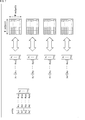
- FIG. 3 It is a figure which shows an example of a sampling function. It is a figure which shows the mode of the pixel control based on the sampling function of FIG. It is a figure which shows an example of a sampling function. It is a figure which shows the mode of the pixel control based on the sampling function of FIG. It is a block diagram which shows the 2nd structural example of an image sensor. It is a figure which shows an example of a sampling function. It is a figure which shows the mode of the pixel control based on the sampling function of FIG. 3 is a flowchart for describing processing of the imaging apparatus in the first configuration example of FIG. 2. It is a block diagram which shows the 2nd structural example of an imaging device and a discrimination
- FIG. 17 It is a figure which shows an example of a sampling function. It is a figure which shows the mode of the pixel control based on the sampling function of FIG. 17 is a flowchart for describing processing of the imaging apparatus in the second configuration example of FIG. 16. It is an equivalent circuit diagram corresponding to the 2nd example of composition of a pixel. It is sectional drawing showing the structure of MOSFET of a pixel. It is a block diagram which shows the structural example (3rd structural example) of the image sensor corresponding to the 2nd structural example of a pixel. It is a timing chart showing the sampling function applicable to the 1st example of composition of a pixel, and the 1st example of composition of an image sensor corresponding to it.
- FIG. 1 illustrates a configuration example of a camera monitoring system according to an embodiment of the present disclosure.
- the camera monitoring system 10 includes a plurality of imaging devices 20, a discrimination server 30, and a behavior analysis device 12. In the case of FIG. 1, five imaging devices 20 are illustrated, but the number of imaging devices 20 can be arbitrarily increased or decreased according to the scale of a facility to which the camera monitoring system 10 is applied.
- the imaging device 20 is connected to the discrimination server 30 via the network 11 and transmits its output to the discrimination server 30 via the network 11.
- the imaging device 20 performs CS (Compressive Sensing) readout in addition to normal readout (driving all pixels of the image sensor mounted on the imaging device 20 to obtain an entire image composed of pixel signals of all pixels). Can do.
- CS Compressive Sensing
- the CS readout means that the imaging surface of the image sensor mounted on the imaging device 20 is divided into blocks of a predetermined size, and a sampling function (details will be described later) among the pixels included in the block for each of the divided blocks.
- This is an operation of generating and outputting a single value (hereinafter referred to as CS data) by driving only pixels that are randomly selected based on the above and performing a predetermined calculation on a pixel signal obtained from the driven pixels. Therefore, at the time of CS reading, CS data can be obtained from each block obtained by dividing the imaging surface of the image sensor.
- the number of pixels to be driven can be reduced as compared with normal reading, so that power consumption can be suppressed.
- the amount of data transmitted to the determination server 30 via the network 11 can be reduced.
- the imaging device 20 directly performs feature detection (detecting a region with a person or a face) from the CS data obtained by CS reading, and only the CS data of the region where the person or the face is detected. Is transferred to the discrimination server 30 via the network 11.
- the imaging device 20 can cut out a pixel signal in a region where a person, a face, or the like is detected, and transfer it to the discrimination server 30 via the network 11.
- the subsequent determination server 30 or the like can also perform video analysis that requires a finer video, such as detecting a facial expression of a person.
- the discrimination server 30 reconstructs an image from CS data of an area in which a person or a face is detected transmitted from the imaging device 20 via the network 11, and performs an identification discrimination process on the reconstructed image.
- the behavior analysis device 12 executes behavior analysis processing of a person who is a subject based on the result of identification discrimination processing by the discrimination server 30.
- FIG. 2 shows a first configuration example of the imaging device 20 and the discrimination server 30.
- FIG. 2 only one imaging device 20 is illustrated, but actually, a plurality of imaging devices 20 are connected to the determination server 30 via the network 11.
- the imaging device 20 in the first configuration example includes a sampling function holding unit 21, a pixel control unit 22, an image sensor 23, an image sensor output holding unit 24, a feature detection unit 25, and a region cutout unit 26.
- the sampling function holding unit 21 holds a plurality of different sampling functions, and supplies the held sampling function to the pixel control unit 22 in response to a request from the pixel control unit 22.
- the sampling function is matrix data indicating which position pixel is driven among pixels included in each block obtained by dividing the imaging surface of the image sensor 23, or data having a format equivalent to the matrix data. .
- a common sampling function is applied to all blocks of the image sensor 23.
- the pixel control unit 22 controls driving of the image sensor 23 (exposure and readout of each pixel). Specifically, the CS reading of the image sensor 23 is controlled by driving a corresponding pixel by applying a common sampling function to each block of the image sensor 23.
- the image sensor 23 drives the pixels in accordance with the control from the pixel control unit 22 to generate CS data for each block, and outputs the generated CS data for each block to the image sensor output holding unit 24 simultaneously or sequentially. To do.
- the image sensor output holding unit 24 holds CS data for each block input from the image sensor 23. Since the CS data of all the blocks held in the image sensor output holding unit 24 is obtained by applying a common sampling function, it is obtained when all the pixels of the image sensor 23 are driven. It can be regarded as a reduced image of the image. Therefore, hereinafter, the CS data of each block obtained by applying a common sampling function held in the image sensor output holding unit 24 is also collectively referred to as a reduced image.
- the feature detection unit 25 performs, for example, a feature detection process for detecting a region having a feature such as a person or a face on the reduced image held in the image sensor output holding unit 24, and the person or the face is detected.
- the area is notified to the area cutout unit 26.
- the region cutout unit 26 cuts out only the region where the feature is detected from the reduced image held in the image sensor output holding unit 24, and transmits it to the discrimination server 30 via the network 11. .
- FIG. 25 For example, multiple templates with rough structures such as partial light and dark patterns of the appearance of faces and people (appearance) are created in advance by a statistical (learning) technique, and the degree of match between the reduced images and those templates It is possible to apply a method that detects all of them. Since this method performs feature detection based on a rough structure, it has a property that feature detection is easy even from a reduced image.
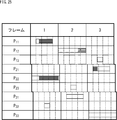
- the image sensor 23 applies four types of different sampling functions per frame to obtain four reduced images.
- a template learned in advance for each sampling function is used. Prepare 4 types. Then, the degree of coincidence with the template learned for each input reduced image is checked, and the possibility of being a detection target (for example, a person) is determined for each block. This determination result is held as a bitmap image equal to the number of blocks, and in determining the reduced image corresponding to the next different sampling function, the held bitmap image is referred to and detected by the determination on the previous reduced image. Only the selected area is subject to the degree of match with the template. As a result, the feature detection processing amount can be reduced.
- the discrimination server 30 in the first configuration example reconstructs an entire image from CS data transmitted from each imaging device 20, for example, as preliminary information for subject flow line analysis, and reconstructs the entire image.
- the identification determination process is performed by comparing with a past history stored in the determination database. Since the CS data transmitted to the discrimination server 30 has already undergone feature detection processing (for example, face detection processing) on the imaging device 20 side, the discrimination server 30 searches for a person from a large amount of video data. There is no need to perform high-load processing, and it is possible to concentrate on identification discrimination processing.
- the entire same as the output at the time of normal reading is performed from the CS data. Processing to reconstruct the image is necessary. According to the CS principle, it is known that the entire image can be reconstructed by using the same sampling function as that applied in the imaging device 20.
- the discrimination server 30 includes an imaging device output holding unit 31, an image reconstruction unit 32, a sampling function holding unit 33, an identification discrimination unit 34, a discrimination DB (Data Base) 35, and a discrimination result DB 36.
- the imaging device output holding unit 31 holds the CS data of the region cut out from the reduced image transmitted from the plurality of imaging devices 20 via the network 11.
- the image reconstruction unit 32 acquires from the sampling function holding unit 33 the same sampling function used by the imaging device 20 when reading CS. Furthermore, the image reconstruction unit 32 restores the entire image from the CS data of the region cut out from the reduced image, which is held in the imaging device output holding unit 31, based on the sampling function.
- the sampling function holding unit 33 holds a plurality of sampling functions like the sampling function holding unit 33 of the imaging apparatus 20 and supplies the sampling function in response to a request from the image reconstruction unit 32.
- the identification discriminating unit 34 collates the entire image from each reconstructed imaging device 20 with each other or collates with the past history stored in the discrimination DB 35 to identify the face already detected. Processing is performed, and the discrimination result is registered in the discrimination result DB 36.
- the identification discrimination result registered in the discrimination result DB 36 is used as preliminary information for subject collinear analysis processing in the behavior analysis device 12.
- FIG. 3 shows a state where the imaging surface of the image sensor 23 is divided into blocks.
- the imaging surface 40 of the image sensor 23 As shown in the figure, on the imaging surface 40 of the image sensor 23, a large number of pixels 42 for converting incident light into electric signals are arranged in a two-dimensional lattice pattern.
- the imaging surface 40 is divided into M ⁇ N blocks in units of blocks composed of K ⁇ L pixels.
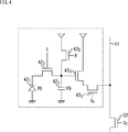
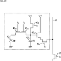
- FIG. 4 shows an equivalent circuit corresponding to the first configuration example of the pixel 42 arranged on the imaging surface 40 of the image sensor 23.
- the pixel 42, PD for converting into an electric signal by photoelectric converting the light incident and (photodiode) 42 1 is formed, PD 42 FD (floating diffusion) through the transfer switch 42 2 in 1 42 3 connected Has been.
- FD 42 3 is connected to the gate of the read AMP42 4, is connected to the read signal line 51 via the read AMP42 4 row selection switch 42 6.
- the FD 42 3 is also connected to the reset switch 4 5 .
- the readout signal line 51 is connected to the column selection switch 52 outside the pixel 42.
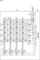
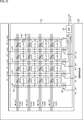
- FIG. 5 shows a first configuration example of the image sensor 23.
- All the pixels 42 in the image sensor 23 are supplied from the pixel controller 22 by a row selection signal line (row sel.), A transfer signal line (trans.), A column selection signal line (col.sel.), And a reset signal line (reset). ) Is driven in accordance with a control signal notified through).
- Pixels belonging to the same row share a row selection signal line, a transfer signal line, and a reset signal line.
- a common readout signal line (read) 51 is connected to the pixels belonging to the same column, and the column selection signal line controls the readout signal line 51 of the corresponding column by the column selection switch 52. Therefore, whether or not each pixel 42 is a pixel signal readout target is controlled by XY addressing using the row selection signal line and the column selection signal line.
- all the pixels 42 belonging to the same block 41 are provided with analog adders (Analog Adders) 53 provided for each block via a common readout signal line 51 and a column selection SW (switch) 52 in units of columns. It is connected to the. In the subsequent stage of the analog adder 53, an ADC 54 is provided for each block.
- Analog Adders Analog Adders
- the pixel signal of the pixel 42 selected by the row selection signal line and the column selection signal is read by the readout signal line 51 wired for each column. Pixel signals read out at the same timing are added by the analog adder 53, and the output of the analog adder 53 is sequentially digitally added by the ADC 54.
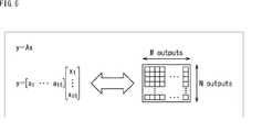
- FIG. 6 shows the relationship between the sampling function, the output value of each block, and the output data format of the image sensor.
- the pixel control unit 22 As described above, of the pixels included in the block, which pixel signal is read out and added is controlled by the sampling function. That is, the pixel control unit 22 generates and outputs a row selection signal, a column selection signal, and a reset signal based on the sampling function.
- the image sensor 23 operates so that a common sampling function A is applied to all the blocks 41 at a certain time, and the output value y at that time is obtained from each block 41.
- a single output value y is obtained from all the blocks 41 simultaneously. be able to. In other words, M ⁇ N two-dimensional array output values y can be obtained.
- the sampling function A can be regarded as a resampling filter having an arbitrary coefficient for 4 ⁇ 4 pixels constituting the block 41, but since a common sampling function is applied to all the blocks 41,
- the M ⁇ N output values y output from the block 41 are also data obtained by performing common resampling on the M ⁇ N two-dimensional grid points from the entire image. Therefore, M ⁇ N output values y can be regarded as a reduced image of M ⁇ N pixels.
- the pixel control unit 22 and the image sensor 23 can perform the above-described operation continuously in time series while switching the sampling function A.
- FIG. 7 shows the relationship between the sampling function that is continuously switched in time series, the output value of each block, and the output data format of the image sensor.
- a 1 [a 11 , a 12 ,..., A 116 ]
- a 2 [a 21 , a 22 ,. .., A 216 ]
- a 3 [a 31 , a 32 ,..., A 316 ]
- a 4 [a 41 , a 42 ,. Is expressed as determinant A.
- the output values y for the sampling functions A 1 , A 2 , A 3 , A 4 are [y 1 , y 2 , y 3 , y 1 ] and M ⁇ N two-dimensional array data (reduced images), respectively. Become.
- each row vector of the sampling function A at least one element may be 1, and the remaining elements may be 0.
- FIG. 8 shows an example of the sampling function A when one of the 16 pixels constituting the block 41 is selected and read out, and is composed of four types (four rows) of row vectors sequentially applied in time series. Is done.
- this sampling function A is applied, one pixel out of 16 pixels constituting the block 41 is read out and output in time series for four pixels.
- FIG. 9 shows a state of control by the pixel control unit 22 based on the sampling function A shown in FIG.
- the row selection signal line and the column selection signal line in the first column are activated, and one pixel in the fourth row and the first column out of 4 ⁇ 4 pixels is selected. Further, the first column of the four column selection switches 52 and the ADC 54 are driven. As a result, the pixel value of one pixel in the fourth row and the first column among the 4 ⁇ 4 pixels is output as a digital signal.
- the same control is performed corresponding to the third row 0 0 0 0 0 0 0 0 0 0 0 1 0 0 0 0 0 0 of the sampling function A in FIG.
- the first pixel in the third row and the second column among the 4 ⁇ 4 pixels in each block 41, the second column among the four column selection switches 52, and the ADC 54 are driven.
- the pixel value of one pixel in the third row and the second column among the 4 ⁇ 4 pixels is output as a digital signal.
- the same control is performed corresponding to the fourth line 0 0 0 1 0 0 0 0 0 0 0 0 0 0 0 0 0 of the sampling function A in FIG.
- the first pixel in the first row and the fourth column among the 4 ⁇ 4 pixels in each block 41, the fourth column among the four column selection switches 52, and the ADC 54 are driven. Thereby, the pixel value of one pixel in the first row and the fourth column among the 4 ⁇ 4 pixels is output as a digital signal.
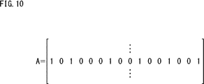
- FIG. 10 shows an example of the sampling function A when selecting and reading out six pixels out of the 16 pixels constituting the block 41.
- FIG. 10 only one type (one row) of row vectors is shown. ing.
- this sampling function A is applied, 6 out of 16 pixels constituting the block 41 are read out, added and output.
- FIG. 11 shows a pixel 42 driven by the pixel control unit 22 based on the sampling function A shown in FIG.
- the pixels are read in four phases according to the number of rows of the block 41.
- the row selection signal line of the first row in the block 41 and the column selection signal lines of the first column and the third column are activated, and 2 in the first row and the first column and the first row and the third column of 4 ⁇ 4 pixels.
- a pixel is selected.
- the first and third columns of the four column selection switches 52, the analog adder 53, and the ADC 54 are driven.
- the pixel values of the two pixels in the first row and the first column and the first row and the third column in the 4 ⁇ 4 pixels are converted into digital signals and held in the counter in the ADC 54.
- the same control is performed corresponding to the elements 0 0 1 0 from the fifth column to the eighth column in the row vector of the sampling function A in FIG.
- one pixel in the second row and the third column among the 4 ⁇ 4 pixels is selected.
- the third column of the four column selection switches 52, the analog adder 53, and the ADC 54 are driven.
- the pixel value of one pixel in the second row and the third column among the 4 ⁇ 4 pixels is converted into a digital signal, and added to and held in the counter in the ADC 54.
- the same control is performed corresponding to the elements 0 1 0 0 from the ninth column to the twelfth column of the row vector of the sampling function A in FIG. 10, which is shown in FIG. 11C.
- one pixel in the third row and the second column among the 4 ⁇ 4 pixels is selected.
- the second column of the four column selection switches 52, the analog adder 53, and the ADC 54 are driven.
- the pixel value of one pixel in the third row and second column among the 4 ⁇ 4 pixels is converted into a digital signal, and added to and held in the counter in the ADC 54.
- the same control is performed corresponding to the elements 1 0 0 1 from the 13th column to the 16th column in the row vector of the sampling function A in FIG.
- 2 pixels in 4 rows and 1 column and 4 rows and 4 columns of 4 ⁇ 4 pixels are selected.
- the first and third columns of the four column selection switches 52, the analog adder 53, and the ADC 54 are driven.
- the pixel values of the two pixels in the 4th row and the 1st column and the 4th row and the 4th column among the 4 ⁇ 4 pixels are converted into digital signals, added to the counter in the ADC 54, and then output to the subsequent stage.
- FIG. 12 shows a second configuration example of the image sensor 23.
- This second configuration example is obtained by replacing the column selection switch 52 with a column selection switch 61 and adding an analog sign inverter 62 to the first configuration example shown in FIG. Since the same reference numerals are given to the components common to the configuration example, the description thereof is omitted as appropriate.
- the column selection switch 61 is connected to the analog adder 53 and the analog sign inverter 62 on the output side, and the pixel signal read from the pixel 42 is analog added in accordance with control from the pixel control unit 22 via the column selection signal. Is output to the converter 53 or the analog sign inverter 62.
- the analog sign inverter 62 is connected to the analog adder 53 on the output side, adds a negative sign to the input pixel signal, and outputs it to the analog adder 53.
- the pixel signal of the pixel corresponding to the sampling function A out of the 16 pixels configuring the block 41 is read and added or subtracted. After that, it can be output as a digital signal.
- FIG. 13 shows an example of a sampling function A that can be applied to the second configuration example of the image sensor 23.
- the pixel value is read and added for the pixel corresponding to 1, and the pixel value is read and subtracted for the pixel corresponding to -1.
- the pixel value is not read (not driven) for the pixel corresponding to 0.
- FIG. 14 shows a pixel 42 driven by the pixel control unit 22 based on the sampling function A shown in FIG.
- the pixels are read in four phases according to the number of rows of the block 41.
- the first row selection signal line and the first and second column selection signal lines in each block 41 are activated, and the first row, first column and first row, second column of 4 ⁇ 4 pixels are activated. Two pixels are selected.
- the output destination of the column selection switch 61 in the first column is the analog adder 53
- the output destination of the column selection switch 61 in the second column is the analog sign inverter 62. Further, the analog adder 53, the analog sign inverter 62, and the ADC 54 are driven.
- a pixel value in which the sign of the pixel in the first row and the third column is inverted negatively is added to the pixel value of the pixel in the first row and the first column among the 4 ⁇ 4 pixels, and then converted into a digital signal. It is held in a counter in the ADC 54.
- the pixel value in which the sign of the pixel in the second row and the fourth column is negatively inverted is added to the pixel value in which the sign of the pixel in the second row and the first column among the 4 ⁇ 4 pixels is inverted. Later, it is converted into a digital signal and added to and held in a counter in the ADC 54.
- the pixel value of the pixel in the 4th row and the 4th column is added to the pixel value obtained by inverting the sign of the pixel in the 4th row and the 1st column out of the 4 ⁇ 4 pixels, and converted into a digital signal. , Added to the counter in the ADC 54 and output to the subsequent stage.
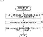
- FIG. 15 is a flowchart for explaining the operation of the imaging apparatus 20 in the first configuration example of FIG.
- step S ⁇ b> 1 the pixel control unit 22 acquires a sampling function that has been negotiated with the discrimination server 30 in advance from the sampling function holding unit 21, and drives the image sensor 23 according to the acquired sampling function. As a result, reduced pixels (CS data for each M ⁇ N block) are output from the image sensor 23 and held in the image sensor output holding unit 24.
- step S ⁇ b> 2 the feature detection unit 25 performs feature detection processing for detecting a region having a feature such as a person or a face, for example, for the reduced image held in the image sensor output holding unit 24.
- the area extraction unit 26 is notified of the area in which is detected.
- step S ⁇ b> 3 in accordance with the notification from the feature detection unit 25, the region cutout unit 26 cuts out only the region in which a person or face is detected from the reduced image held in the image sensor output holding unit 24 and uses the network 11. To the discrimination server 30. Thus, the operation for one frame of the imaging device 20 in the first configuration example is completed.
- the imaging device 20 in the first configuration example performs CS reading according to the sampling function, so that power consumption can be suppressed. Moreover, since only the area
- the identification discrimination process can be performed without executing the feature detection process again, thereby reducing the processing load on the discrimination server 30 side. Can do.
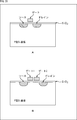
- FIG. 16 illustrates a second configuration example of the imaging device 20 and the discrimination server 30.
- symbol is attached
- the image pickup apparatus 20 in the first configuration example shown in FIG. 2 performs CS readout by applying a common sampling function to all blocks of the image sensor 23 to obtain a reduced image.
- the imaging device 20 in the second configuration example does not necessarily apply a common sampling function to all blocks, and a sampling function different from the common sampling function for a specific block. Can be applied.
- the imaging device 20 in the second configuration example can apply a sampling function that means reading of all pixels to a block in a region where a feature (such as a face) is detected. .
- the imaging device 20 in the second configuration example includes a sampling function holding unit 21, a pixel control unit 22, an image sensor 23, an image sensor output holding unit 24, a resampling unit 71, a reduced image holding unit 72, a feature detection unit 73, and The area cutout unit 26 is configured.
- the sampling function holding unit 21 holds a plurality of different sampling functions, and supplies the held sampling function in response to a request from the pixel control unit 22 or the resampling unit 71.
- a sampling function that is commonly applied to each block of the image sensor 23 and a sampling function that is applied to a specific block is read out.
- Stuff is supplied.
- a sampling function that is commonly applied to each block of the image sensor 23 is supplied to the resampling unit 71.
- the pixel control unit 22 controls driving of the image sensor 23 (exposure and readout of each pixel). Specifically, the CS reading of the image sensor 23 is controlled by driving only the pixels corresponding to the common sampling function for each block of the image sensor 23. Furthermore, in the case of the second configuration example, the pixel control unit 22 can apply a sampling function different from a sampling function commonly applied to other blocks to a specific block. Specifically, for example, a sampling function for reading out all pixels can be applied to a block around a region where a feature is detected, which is notified from the feature detection unit 73.
- the image sensor 23 outputs CS data for each block to the image sensor output holding unit 24 by driving the pixels and the like according to the control from the pixel control unit 22.
- the image sensor output holding unit 24 holds CS data for each block input from the image sensor 23.
- the CS data of each block held in the image sensor output holding unit 24 may not be applied with a common sampling function. Can not.
- the resampling unit 71 acquires CS data for each block held in the image sensor output holding unit 24, and applies a common sampling function to the CS data for each block acquired from the sampling function holding unit 21. Sampling processing is performed, and the processing result is held in the reduced image holding unit 72.
- the resampling processing result held in the reduced image holding unit 72 can be regarded as a reduced image because a common sampling function is applied. Further, among the CS data for each block held in the image sensor output holding unit 24, the resampling process can be omitted for the data to which the common sampling function is applied.
- the feature detection unit 73 detects, for example, a region having a feature such as a person or a face from the reduced image held in the reduced image holding unit 72 by a feature detection process similar to that of the feature detection unit 25 in FIG. Then, the area extraction unit 26 and the pixel control unit 22 are notified of the area in which a person or a face is detected.
- the region cutout unit 26 cuts out the CS data for each block held in the image sensor output holding unit 24 that corresponds to the region in which a person or face is detected, The data is transmitted to the discrimination server 30 via the network 11.
- the CS data for each block held in the image sensor output holding unit 24 the CS data of a specific block (a block around the area where the feature is detected in the previous feature detection process) is stored in the block. It is the pixel value itself of all the pixels to which it belongs. Therefore, the pixel values of all the pixels of the block belonging to the area where the feature is detected are transmitted to the discrimination server 30.
- the discrimination server 30 in the second configuration example is the discrimination server 30 in the first configuration example shown in FIG. Therefore, the image reconstructing unit 32 and the sampling function holding unit 33 can be omitted. Since the other components of the discrimination server 30 in the second configuration example are the same as those in the first configuration example, description thereof is omitted.
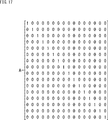
- FIG. 17 illustrates an example of a sampling function that is applied to a specific block by the pixel control unit 22 and is different from a sampling function that is commonly applied to other blocks.
- sampling function A In the sampling function A of 16 rows and 16 columns, only one element of each row vector has a value of 1, and the other 15 elements have a value of 0.
- FIG. 18 shows a state of control by the pixel control unit 22 based on the sampling function A shown in FIG.
- the sampling function A in FIG. 17 corresponding to the first row 1 0 0 0 0 0 0 0 0 0 0 0 0 0 0 0 0 0 of the sampling function A in FIG. 17, one row in the corresponding block 41 as shown in FIG.
- the first row selection signal line and the first column selection signal line are activated, and one pixel in the first row and the first column out of 4 ⁇ 4 pixels is selected. Further, the first column of the four column selection switches 52 and the ADC 54 are driven. Thereby, the pixel value of one pixel in the first row and the first column among the 4 ⁇ 4 pixels is output as a digital signal.
- the same control is performed corresponding to the third row 0 0 1 0 0 0 0 0 0 0 0 0 0 0 0 0 0 of the sampling function A in FIG.
- the first pixel in the first row and the third column among the 4 ⁇ 4 pixels in the corresponding block 41, the third column among the four column selection switches 52, and the ADC 54 are driven.
- the pixel value of one pixel in the first row and the third column among the 4 ⁇ 4 pixels is output as a digital signal.
- the description and illustration thereof are omitted, but similarly, the pixel value of one pixel of the 4 ⁇ 4 pixels in the corresponding block 41 is output as a digital signal.
- the ADC is provided for each block. If this is used, it is possible to output a control signal for reading out all pixels only in a specific block by shifting the timing at which the selection control signal is given in units of block rows instead of synchronizing all the blocks. If the ADC of the block is driven at high speed in accordance with this, it is possible to mix blocks driven according to different sampling functions. Note that blocks driven according to different sampling functions can also be mixed by shifting the timing of supplying the selection control signal in units of blocks.
- FIG. 19 is a flowchart for explaining the operation of the imaging apparatus 20 in the second configuration example of FIG.
- step S11 the pixel control unit 22 acquires a sampling function to be applied to a specific block and a sampling function to be commonly applied to blocks other than the specific block from the sampling function holding unit 21, and acquires the acquired sampling function.
- the image sensor 23 is driven according to the function.
- the CS data of each block is output from the image sensor 23 and held in the image sensor output holding unit 24.
- step S ⁇ b> 12 the resampling unit 71 acquires CS data of each block held in the image sensor output holding unit 24, and applies it in common to each block of the image sensor 23 from the sampling function holding unit 21. Get the sampling function to be performed. Further, the resampling unit 71 generates a reduced image by applying a common sampling function to the acquired CS data of each block, and holds the reduced image in the reduced image holding unit 72.
- step S ⁇ b> 13 the feature detection unit 73 performs feature detection processing for detecting an area having features such as a person and a face for the reduced image held in the reduced image holding unit 72. The detected area is notified to the area cutout unit 26 and the pixel control unit 22.
- step S ⁇ b> 14 the region cutout unit 26 corresponds to a region in which a person or a face is detected in the CS data of each block held in the image sensor output holding unit 24 in accordance with the notification from the feature detection unit 73. Only a thing is cut out and transmitted to the discrimination server 30 via the network 11. However, as for the CS data for each block held in the image sensor output holding unit 24, the CS data of a specific block (a block around the area where the feature is detected in the previous feature detection process) is stored in the block. It is the pixel value itself of all the pixels to which it belongs. Therefore, the pixel values of all the pixels of the block belonging to the area where the feature is detected are transmitted to the discrimination server 30. Thus, the operation for one frame of the imaging apparatus 20 in the second configuration example is completed.
- CS reading is performed according to the sampling function, so that power consumption can be suppressed.
- the pixel values of all the pixels are transmitted to the discrimination server 30 for the region where the feature is detected, compared to the case where the entire image obtained by normal reading of the image sensor 23 is transmitted to the discrimination server 30 as it is, Data communication can be greatly reduced.
- the discrimination server 30 can perform the identification discrimination process using the pixel values of all the pixels in the region where the feature is detected without executing the feature detection process again, the processing load on the discrimination server 30 side In addition to being able to reduce, detailed image analysis and behavior analysis can be performed.
- FIG. 20 shows an equivalent circuit corresponding to the second configuration example of the pixel 42 arranged on the imaging surface 40 of the image sensor 23.
- the second configuration example of the pixel 42 is obtained by replacing the transfer switch 42 2 in the first configuration example shown in FIG. 4 with multi-bit transfer switches 42 21 and 42 22 , and other components. Is the same as that in the first configuration example, and is therefore given the same reference numeral.
- FIG. 21 is a cross-sectional view showing the structure of the MOSFET of the pixel 42.
- 4A corresponds to the first configuration example of the pixel 42 shown in FIG. 4
- FIG. 3B corresponds to the second configuration example of the pixel 42 shown in FIG. is there.
- the MOSFET is a semiconductor having the same property (in this case, N-type) in the source and drain, and the opposite property in the channel region immediately below the gate (in the same figure). In this case, it is formed by arranging a semiconductor having P-type).
- the source can have a current inlet
- the drain can have an outlet
- the gate can have a sluice function to control the current flow.
- the semiconductor is electrically insulated because a semiconductor having different properties is sandwiched between the source and the drain.
- a voltage is applied to the gate, free electrons are attracted to the channel region immediately below the gate. For this reason, the free electrons are abundant in all the paths connecting the source and the drain, and the current easily flows.
- Gate 1 shown in the same drawing B corresponds the transfer switch 42 21, 42 22 in the second configuration example. In the second configuration example, only if at the same time the voltage to the transfer switch 42 21, 42 22 is applied, a current flows easily.
- FIG. 22 shows a configuration example (third configuration example) of the image sensor corresponding to the second configuration example of the pixel 42.
- the third configuration example is a row transfer signal in which the transfer signal line (trans.) In the first configuration example shown in FIG. 5 is connected to multi-bit transfer switches 42 21 and 42 22 of each pixel 42. It is replaced with a line (row trans.) And a column transfer signal line (col.trans.), And other common components are denoted by the same reference numerals.
- each pixel 42 of the image sensor 23 without being limited to the reset timing of the FD 42 3 may transfer PD 42 1 of accumulated charge at an arbitrary timing.
- the pixel signal of each pixel can be sampled at an arbitrary exposure time. In other words, the pixel signal of each pixel can be randomly added temporally and spatially.
- the first configuration example of the pixel 42 and the first configuration example of the image sensor 23 corresponding thereto are possible, and the pixel signal of each pixel is randomly sampled temporally and spatially.
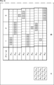
- An example of the sampling function is shown in FIG.
- FIG. B shows the sampling function as a timing chart, and the rows indicate the sampling timing of each pixel, and sampling is performed at colored squares.
- the column indicates the sampling timing.
- data for one frame (solid line break) is sampled in five times (broken line break), and sampling is performed a total of 15 times for three frames.
- the fact that the columns are slightly shifted in units of 3 rows indicates that the readout of each row is slightly shifted in time by the focal plane readout of the pixel signal from the pixel 42.
- the time difference is less than 1H, it can be considered that the readout of 9 pixels constituting one lock is simultaneous.
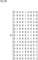
- FIG. 24 shows a sampling function in matrix notation corresponding to the timing chart shown in B of FIG. As shown in the figure, since sampling is performed a total of 15 times in three frames, the sampling function is expressed as a matrix of 15 rows and 9 columns by collecting 15 rows of 9 element row vectors.
- FIG. 25 illustrates a case where the second configuration example of the pixel 42 and the third configuration example of the image sensor 23 corresponding thereto are possible, and pixel signals of each pixel are randomly added temporally and spatially. An example of a sampling function is shown.
- FIG. 26 shows a sampling function of a matrix expression corresponding to the timing chart shown in FIG.
- a coefficient other than 1, for example, 3 in the 4th row and the 1st column means that when a sampling interval is 1, a signal having a continuous exposure period of 3 times is sampled.
- FIG. 27 shows an equivalent circuit corresponding to a third configuration example of the pixel 42 arranged on the imaging surface 40 of the image sensor 23.
- the third configuration example of the pixel 42 is for the reset switch 42 5 in the second configuration example shown in FIG. 20, was replaced with the reset switch 42 51, 42 52 having the multi-bit of other components Is the same as that in the second configuration example, and is therefore given the same reference numeral.
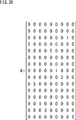
- each pixel regardless of whether it is selected for signal readout, it is possible to control each pixel whether to reset the FD 42 3. If this is used, for example, in the sampling function shown as a timing chart in FIG. 25, if all pixel reset is performed only at the end of the exposure period of each frame, the exposure within the block exposed in different periods within the frame will be performed. A signal obtained by adding these pixels in space can be read out. In this case, the matrix representation of the sampling function is as shown in FIG.
- the output value per frame is a single value
- the row vector of the sampling function corresponding to the output value is the sampling unit in the frame. This is a vector of 45 (9 pixels ⁇ 5 periods) elements, which is the total number.
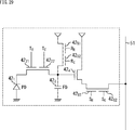
- FIG. 29 shows an equivalent circuit corresponding to a fourth configuration example of the pixel 42 arranged on the imaging surface 40 of the image sensor 23.
- Other constituent elements are the same as those in the third configuration example, and are therefore given the same reference numerals.
- the fourth configuration example of the pixel 42 can operate in the same manner as the third configuration example shown in FIG.
- the camera monitoring system according to the present embodiment can be applied to, for example, a security system that performs suspicious person detection, a system that analyzes behavior of factory workers and shoppers in stores, and the like.
- This indication can also take the following composition.
- An image sensor having an imaging surface in which a large number of pixels are arranged vertically and horizontally; By controlling the image sensor and applying a sampling function to each block obtained by dividing the imaging surface of the image sensor into a plurality of pixels, a pixel corresponding to the sampling function among the pixels constituting the block is selected, A pixel control unit that outputs a sampling signal based on the pixel value of the selected pixel;
- An image pickup apparatus comprising: a reduced image generation unit that generates a reduced image based on the sampling signal for each of the blocks output from the image sensor.
- the image sensor selects one pixel corresponding to the sampling function among the pixels configuring the block according to control from the pixel control unit, and outputs a pixel value of the selected one pixel as the sampling signal.
- (3) The image sensor selects one pixel corresponding to the sampling function among the pixels constituting the block according to a row selection signal and a column selection signal from the pixel control unit.
- the image sensor according to (4) wherein the image sensor randomly selects one of the pixels constituting the block spatially and temporally according to a row selection signal and a column selection signal from the pixel control unit. apparatus.
- the image sensor selects a plurality of pixels corresponding to the sampling function among the pixels constituting the block in accordance with control from the pixel control unit, and adds an added value obtained by adding pixel values of the selected plurality of pixels.
- the imaging device according to (1) wherein the imaging device outputs the sampling signal.
- the image sensor is An analog adder for adding pixel values of pixels selected by a row selection signal and a column selection signal from the pixel control unit for each row;
- each pixel of the image sensor includes a multi-bit transfer switch that performs switching based on the row selection signal and the column selection signal from the pixel control unit.
- the image sensor according to a row selection signal and a column selection signal from the pixel control unit, randomly selects a plurality of pixels among the pixels constituting the block spatially and temporally as described in (8). Imaging device.
- the image sensor selects a plurality of pixels corresponding to the sampling function among the pixels constituting the block according to control from the pixel control unit, and positive or negative signs are added to pixel values of the selected plurality of pixels.
- the image pickup apparatus according to (1) wherein an addition value obtained by adding and adding is output as the sampling signal.
- the image sensor is An analog adder for adding pixel values of pixels selected by a row selection signal and a column selection signal from the pixel control unit for each row; A sign inversion unit for inverting the sign of the output from the analog addition unit;
- the imaging apparatus according to (1) or (10) further including: an ADC unit that sequentially digitally adds outputs for each row from the analog addition unit or the sign inversion unit.
- each pixel of the image sensor includes a multi-bit transfer switch that performs switching based on the row selection signal and the column selection signal from the pixel control unit.
- the image sensor according to a row selection signal and a column selection signal from the pixel control unit, randomly selects a plurality of pixels among the pixels constituting the block spatially and temporally as described in (12).
- Imaging device (14)
- the pixel control unit controls the image sensor, and applies a common sampling function to each block obtained by dividing the imaging surface of the image sensor into a plurality of blocks, whereby the common pixel among the pixels constituting the block is used.
- the imaging apparatus wherein the reduced image generation unit generates the reduced image based on the sampling signal for each block to which the common sampling function output from the image sensor is applied.
- the pixel control unit controls the image sensor and applies a common sampling function or a non-common sampling function different from the common sampling function for each block obtained by dividing the imaging surface of the image sensor into a plurality of blocks.
- the reduced image generation unit is configured to change the sampling signal for each block to which the common sampling function or the non-common sampling function output from the image sensor is applied, to the common sampling function.
- the reduced-size image is generated by re-sampling the sampling signal based on the imaging device according to (1).
- a non-common sampling function different from the sampling function is applied, and the common sampling function is applied to a block corresponding to a region in which no feature is detected by the feature detection process, so that the pixels constituting the block Selecting a pixel corresponding to the common sampling function or the non-common sampling function, and outputting a sampling signal based on a pixel value of the selected pixel;
- the region cutout unit cuts out the sampling signal of the block to which the non-common sampling function is applied, corresponding to the region in which the feature is detected by the feature detection process, from the output of the image sensor, and
- the imaging device according to (17).
- the imaging device An image sensor having an imaging surface in which a large number of pixels are arranged vertically and horizontally; By controlling the image sensor and applying a sampling function to each block obtained by dividing the imaging surface of the image sensor into a plurality of pixels, a pixel corresponding to the sampling function among the pixels constituting the block is selected, A pixel control unit that outputs a sampling signal based on the pixel value of the selected pixel; A reduced image generation unit that generates a reduced image based on the sampling signal for each of the blocks output from the image sensor; A feature detection unit that performs feature detection processing on the reduced image; A region cutout unit that cuts out the sampling signal for each block corresponding to a region in which a feature is detected by the feature detection process from the output of the image sensor, and transmits the block to the information processing device via the network;
- the information device includes: An information processing system comprising: an information processing unit that performs predetermined information processing
Landscapes
- Engineering & Computer Science (AREA)
- Multimedia (AREA)
- Signal Processing (AREA)
- Studio Devices (AREA)
- Transforming Light Signals Into Electric Signals (AREA)
- Image Processing (AREA)
Abstract
Priority Applications (4)
| Application Number | Priority Date | Filing Date | Title |
|---|---|---|---|
| CN201680040151.7A CN107736014B (zh) | 2015-07-16 | 2016-07-01 | 摄像设备和信息处理系统 |
| JP2017528387A JP6863281B2 (ja) | 2015-07-16 | 2016-07-01 | 撮像装置、および情報処理システム |
| US15/741,921 US10602084B2 (en) | 2015-07-16 | 2016-07-01 | Imaging apparatus which performs compressive sensing reading data for a partitioned block output from an image sensor |
| CN202011464687.6A CN112738365B (zh) | 2015-07-16 | 2016-07-01 | 成像设备和信息处理系统 |
Applications Claiming Priority (2)
| Application Number | Priority Date | Filing Date | Title |
|---|---|---|---|
| JP2015141882 | 2015-07-16 | ||
| JP2015-141882 | 2015-07-16 |
Publications (1)
| Publication Number | Publication Date |
|---|---|
| WO2017010316A1 true WO2017010316A1 (fr) | 2017-01-19 |
Family
ID=57757221
Family Applications (1)
| Application Number | Title | Priority Date | Filing Date |
|---|---|---|---|
| PCT/JP2016/069646 Ceased WO2017010316A1 (fr) | 2015-07-16 | 2016-07-01 | Dispositif de capture d'image et système de traitement d'informations |
Country Status (4)
| Country | Link |
|---|---|
| US (1) | US10602084B2 (fr) |
| JP (1) | JP6863281B2 (fr) |
| CN (2) | CN112738365B (fr) |
| WO (1) | WO2017010316A1 (fr) |
Cited By (3)
| Publication number | Priority date | Publication date | Assignee | Title |
|---|---|---|---|---|
| WO2020012756A1 (fr) * | 2018-07-13 | 2020-01-16 | マクセル株式会社 | Dispositif de formation d'images stéréoscopiques |
| JP2020043614A (ja) * | 2018-08-31 | 2020-03-19 | ソニー株式会社 | 撮像装置、撮像システム、撮像方法および撮像プログラム |
| JP2023041576A (ja) * | 2021-09-13 | 2023-03-24 | エスケーハイニックス株式会社 | イメージセンサの動作方法 |
Families Citing this family (2)
| Publication number | Priority date | Publication date | Assignee | Title |
|---|---|---|---|---|
| JP6806494B2 (ja) * | 2016-08-24 | 2021-01-06 | キヤノン株式会社 | 撮像装置、撮像システム、移動体及び撮像装置の駆動方法 |
| US12184956B2 (en) * | 2021-07-29 | 2024-12-31 | Omnivision Technologies, Inc. | Color-infrared sensor with a low power binning readout mode |
Citations (3)
| Publication number | Priority date | Publication date | Assignee | Title |
|---|---|---|---|---|
| JP2004266369A (ja) * | 2003-02-21 | 2004-09-24 | Sony Corp | 固体撮像装置およびその駆動方法 |
| JP2008035279A (ja) * | 2006-07-28 | 2008-02-14 | Sanyo Electric Co Ltd | 画素情報読出方法および撮像装置 |
| JP2010055594A (ja) * | 2008-07-31 | 2010-03-11 | Nec Software Kyushu Ltd | 動線管理システムおよびプログラム |
Family Cites Families (16)
| Publication number | Priority date | Publication date | Assignee | Title |
|---|---|---|---|---|
| JPS5558670A (en) * | 1978-10-25 | 1980-05-01 | Ricoh Co Ltd | Picture processing system |
| JP3733873B2 (ja) * | 2001-06-07 | 2006-01-11 | ノーリツ鋼機株式会社 | 写真画像処理装置、方法及び写真処理装置 |
| JP4403687B2 (ja) * | 2002-09-18 | 2010-01-27 | ソニー株式会社 | 固体撮像装置およびその駆動制御方法 |
| JP4290066B2 (ja) * | 2004-05-20 | 2009-07-01 | キヤノン株式会社 | 固体撮像装置および撮像システム |
| US7978240B2 (en) * | 2005-10-03 | 2011-07-12 | Konica Minolta Photo Imaging, Inc. | Enhancing image quality imaging unit and image sensor |
| CN2838168Y (zh) * | 2005-10-19 | 2006-11-15 | 上海广电(集团)有限公司中央研究院 | 用于图像显示的截断误差补偿装置 |
| US7944482B2 (en) * | 2006-07-28 | 2011-05-17 | Sanyo Electric Co., Ltd. | Pixel information readout method and image pickup apparatus |
| JP4867554B2 (ja) * | 2006-09-29 | 2012-02-01 | カシオ計算機株式会社 | 電子カメラ、撮像制御プログラム及び撮像制御方法 |
| US8169495B2 (en) * | 2006-12-01 | 2012-05-01 | Broadcom Corporation | Method and apparatus for dynamic panoramic capturing |
| GB0709026D0 (en) * | 2007-05-10 | 2007-06-20 | Isis Innovation | High speed imaging with slow scan cameras using pixel level dynami shuttering |
| US20090219418A1 (en) * | 2008-02-29 | 2009-09-03 | Hiroaki Fujita | Image sensor and method to reduce dark current of cmos image sensor |
| JP5140638B2 (ja) * | 2009-06-22 | 2013-02-06 | 日本放送協会 | 空間ダウンサンプリング処理装置、空間アップサンプリング処理装置、符号化装置、復号装置及びプログラム |
| FR2959901B1 (fr) * | 2010-05-04 | 2015-07-24 | E2V Semiconductors | Capteur d'image a matrice d'echantillonneurs |
| JP5845140B2 (ja) * | 2011-06-29 | 2016-01-20 | キヤノン株式会社 | 撮像素子及び撮像装置 |
| CN203894772U (zh) * | 2014-03-11 | 2014-10-22 | 深圳市中安视科技有限公司 | 一种海量人脸发现与识别系统 |
| US20150334299A1 (en) * | 2014-05-14 | 2015-11-19 | Panasonic Intellectual Property Management Co., Ltd. | Monitoring system |
-
2016
- 2016-07-01 CN CN202011464687.6A patent/CN112738365B/zh active Active
- 2016-07-01 US US15/741,921 patent/US10602084B2/en active Active
- 2016-07-01 CN CN201680040151.7A patent/CN107736014B/zh active Active
- 2016-07-01 JP JP2017528387A patent/JP6863281B2/ja active Active
- 2016-07-01 WO PCT/JP2016/069646 patent/WO2017010316A1/fr not_active Ceased
Patent Citations (3)
| Publication number | Priority date | Publication date | Assignee | Title |
|---|---|---|---|---|
| JP2004266369A (ja) * | 2003-02-21 | 2004-09-24 | Sony Corp | 固体撮像装置およびその駆動方法 |
| JP2008035279A (ja) * | 2006-07-28 | 2008-02-14 | Sanyo Electric Co Ltd | 画素情報読出方法および撮像装置 |
| JP2010055594A (ja) * | 2008-07-31 | 2010-03-11 | Nec Software Kyushu Ltd | 動線管理システムおよびプログラム |
Cited By (13)
| Publication number | Priority date | Publication date | Assignee | Title |
|---|---|---|---|---|
| JP7140580B2 (ja) | 2018-07-13 | 2022-09-21 | マクセル株式会社 | ステレオ撮像装置 |
| JP2020014067A (ja) * | 2018-07-13 | 2020-01-23 | マクセル株式会社 | ステレオ撮像装置 |
| US12267480B2 (en) | 2018-07-13 | 2025-04-01 | Maxell, Ltd. | Stereo imaging device with image distortion correction |
| WO2020012756A1 (fr) * | 2018-07-13 | 2020-01-16 | マクセル株式会社 | Dispositif de formation d'images stéréoscopiques |
| JP7424034B2 (ja) | 2018-08-31 | 2024-01-30 | ソニーグループ株式会社 | 固体撮像素子、撮像装置および認識処理方法 |
| JP2020054007A (ja) * | 2018-08-31 | 2020-04-02 | ソニー株式会社 | 撮像装置、撮像システム、撮像方法および撮像プログラム |
| JP7424051B2 (ja) | 2018-08-31 | 2024-01-30 | ソニーグループ株式会社 | 固体撮像素子、撮像装置、撮像方法および撮像プログラム |
| US12080061B2 (en) | 2018-08-31 | 2024-09-03 | Sony Group Corporation | Imaging apparatus, imaging system, imaging method, and imaging program |
| US12159455B2 (en) | 2018-08-31 | 2024-12-03 | Sony Group Corporation | Imaging apparatus, imaging system, imaging method, and imaging program |
| US12183069B2 (en) | 2018-08-31 | 2024-12-31 | Sony Group Corporation | Imaging apparatus, imaging system, imaging method, and imaging program |
| JP2020043614A (ja) * | 2018-08-31 | 2020-03-19 | ソニー株式会社 | 撮像装置、撮像システム、撮像方法および撮像プログラム |
| JP2023041576A (ja) * | 2021-09-13 | 2023-03-24 | エスケーハイニックス株式会社 | イメージセンサの動作方法 |
| JP7809493B2 (ja) | 2021-09-13 | 2026-02-02 | エスケーハイニックス株式会社 | イメージセンサの動作方法 |
Also Published As
| Publication number | Publication date |
|---|---|
| JP6863281B2 (ja) | 2021-04-21 |
| CN107736014B (zh) | 2020-12-18 |
| CN107736014A (zh) | 2018-02-23 |
| JPWO2017010316A1 (ja) | 2018-04-26 |
| CN112738365B (zh) | 2022-11-18 |
| CN112738365A (zh) | 2021-04-30 |
| US20180205895A1 (en) | 2018-07-19 |
| US10602084B2 (en) | 2020-03-24 |
Similar Documents
| Publication | Publication Date | Title |
|---|---|---|
| JP6863281B2 (ja) | 撮像装置、および情報処理システム | |
| US10531069B2 (en) | Three-dimensional image sensors | |
| TWI430186B (zh) | 影像處理裝置及影像處理方法 | |
| US10225441B2 (en) | Time delay and integration (TDI) imaging sensor and method | |
| KR101747214B1 (ko) | 다채널 영상 분석 방법 및 시스템 | |
| CN102572508A (zh) | 一种视频故障诊断系统及方法 | |
| JP2024000518A (ja) | クロップされた画像を使用した物体検出のための方法 | |
| Goyal et al. | Photon-starved scene inference using single photon cameras | |
| JP5909711B1 (ja) | 動線分析システム及び動線表示方法 | |
| US8390685B2 (en) | Virtual fence | |
| CN110401797A (zh) | 用于低功率视觉传感器的方法和系统 | |
| CN109101884B (zh) | 一种脉冲阵列预测方法 | |
| KR101701138B1 (ko) | 해상도 및 초점 향상 | |
| US10321160B2 (en) | Compressing multiple video files using localized camera meta data | |
| WO2025026636A1 (fr) | Agencement de tdc 2d | |
| US10326950B1 (en) | Image capture at multiple resolutions | |
| CN117692812A (zh) | 一种图像处理方法、电子设备、存储介质和产品 | |
| JP2021019288A (ja) | 撮像装置およびその制御方法 | |
| US9344648B2 (en) | High dynamic range imaging | |
| KR102588413B1 (ko) | 히트맵을 생성하는 장치 및 방법 | |
| WO2025057684A1 (fr) | Système de traitement d'image et système de traitement d'informations | |
| KR20220169511A (ko) | 영상 예측 생성적 적대 신경망 기반 영상 예측 장치 및 방법 | |
| Da Luz et al. | Activities of daily living classification using depth features | |
| Saypadith et al. | Abnormal Event Detection using Joint Spatiotemporal Learning | |
| KR101793164B1 (ko) | 저장 공간을 절감하기 위한 영상 처리 장치, 영상 복원 장치 및 영상 관리 장치 |
Legal Events
| Date | Code | Title | Description |
|---|---|---|---|
| 121 | Ep: the epo has been informed by wipo that ep was designated in this application |
Ref document number: 16824296 Country of ref document: EP Kind code of ref document: A1 |
|
| ENP | Entry into the national phase |
Ref document number: 2017528387 Country of ref document: JP Kind code of ref document: A |
|
| WWE | Wipo information: entry into national phase |
Ref document number: 15741921 Country of ref document: US |
|
| NENP | Non-entry into the national phase |
Ref country code: DE |
|
| 122 | Ep: pct application non-entry in european phase |
Ref document number: 16824296 Country of ref document: EP Kind code of ref document: A1 |